JP4804635B2 - GaN-based field effect transistor - Google Patents
GaN-based field effect transistor Download PDFInfo
- Publication number
- JP4804635B2 JP4804635B2 JP2001062323A JP2001062323A JP4804635B2 JP 4804635 B2 JP4804635 B2 JP 4804635B2 JP 2001062323 A JP2001062323 A JP 2001062323A JP 2001062323 A JP2001062323 A JP 2001062323A JP 4804635 B2 JP4804635 B2 JP 4804635B2
- Authority
- JP
- Japan
- Prior art keywords
- gan
- gate electrode
- active layer
- layer
- fet
- Prior art date
- Legal status (The legal status is an assumption and is not a legal conclusion. Google has not performed a legal analysis and makes no representation as to the accuracy of the status listed.)
- Expired - Lifetime
Links
Images


Landscapes
- Junction Field-Effect Transistors (AREA)
Description
【0001】
【発明の属する技術分野】
本発明はGaN系電界効果トランジスタ(FET)に関し、更に詳しくは、オン抵抗が小さく、ピンチオフ状態を実現しやすく、また、高温動作と大電流駆動が可能なスイッチング素子として有用な新規構造のGaN系FETに関する。
【0002】
【従来の技術】
最近、MIS(金属−絶縁層−半導体)構造を有するFETの開発研究が進められているが、その場合、用いる化合物半導体としてはGaAs系が主流となっている。
そのGaAs系FETは概ね次のようにして製造されている。まず、サファイア基板のような基板の上に、例えばMOCVD法により、ノンドープGaAsから成る半絶縁層を形成し、更にその上に、Siドープn−AlGaAsから成る活性層を形成する。そして、この活性層の上に、例えばプラズマCVD法でSiO2膜を成膜し、ここに、フォトリソグラフィーとエッチングを行って所望パターンの開口部を形成し、更にその開口部から所定の電極材料を蒸着して、前記活性層(Siドープn−AlGaAs層)の上にゲート電極、ソース電極、ドレイン電極などの動作電極を形成する。
【0003】
ところで、最近のFETに関しては、例えば自動車に搭載するスイッチング素子としての用途が広がりはじめている。このような用途分野のFETに対しては、軽量化、小型化への要望とともに、エンジンルーム内の温度を考慮して高温動作が可能で、そして大電流駆動が可能であることも要求されている。この後者の要求との関係では、上記したGaAs系FETは必ずしも満足すべき特性を発揮するものではない。
【0004】
一方、GaN,AlGaN,InGaAlNのようなGaN系化合物半導体は、GaAsやSiなどに比べて高温動作が可能であり、またヘテロ接合界面における不連続バンドギャップが広いので、これをゲート電極が形成される活性層として使用すれば、高温動作をするとともに、高電圧も印加できるFETを得ることができる。
【0005】
このようなことから、GaN系化合物半導体を用いたFETの開発研究が進められているが、現在までに得られているGaN系FETには、従来のSiやGaAs系FETに比べればその動作時のオン抵抗が1桁から3桁程度小さくなるという利点を備えているとはいえ、結晶成長技術の未成熟や電極形成技術の未成熟により、依然として可成りのオン抵抗が存在している。
【0006】
また、ゲート電極からその直下に位置する活性層にかなりの高電界を印加した場合であっても、そのゲート部にはチャネルを完全に遮断する空乏層が形成されず、そのため満足すべきピンチオフ状態を実現せず、ソース電極とドレイン電極の間にリーク電流の流れることがある。
【0007】
【発明が解決しようとする課題】
本発明はGaN系FETにおける上記した問題を解決し、オン抵抗が小さく、かつリーク電流を発生させずピンチオフ状態を得やすくした構造になっていて、GaN系材料の特性を充分に生かすように設計されたGaN系FETの提供を目的とする。
【0008】
【課題を解決するための手段】
上記した目的を達成するために、本発明においては、半絶縁性基板の上に、形成すべきゲート電極と同一の材料から成る下部ゲート電極が、直接、前記ゲート電極と同一のパターンで形成され、前記下部ゲート電極を埋設してGaN系化合物半導体から成る少なくとも1層の活性層が形成され、前記活性層の上面には前記ゲート電極が形成され、前記活性層を挟んで上下にゲート電極が配置されていることを特徴とするGaN系電界効果トランジスタが提供される。
【0009】
【発明の実施の形態】
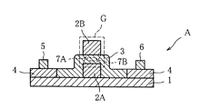
本発明のGaN系FETの基本構成Aを図1に示す。
このGaN系FET(A)では、半絶縁性基板1の上に、直接、下部ゲート電極2Aが配線され、それを埋設してGaN系化合物半導体から成る活性層3が配置され、その活性層3の上面にはゲート電極2Bが形成されている。
【0010】
ここで、ゲート電極2Bはある設計パターンで活性層3の上面に配線されていて、それと対応する半絶縁性基板1の表面位置に、下部ゲート電極2Aが上記ゲート電極2Bと同じ設計パターンで配線され、そしてその下部ゲート電極2Aが活性層3に埋設されている。したがって、図1の破線領域として示したように、活性層3は上下に配線された下部ゲート電極2Aとゲート電極2Bで挟まれることにより、ゲート部Gが形成されている。
【0011】
そして、活性層3の両側部、具体的にいえば、上記したゲート部Gを除いた領域の半絶縁性基板1の上には、直接、コンタクト層4,4が配置され、それらの上には、それぞれ、ソース電極5とドレイン電極6が形成されている。
このFET(A)の場合、ゲート部Gが活性層3とそれを上下から挟む2個のゲート電極2A,2Bで構成されているので、これらゲート電極を動作して活性層3に電界を印加すると、まず、ゲート電極2Bにより活性層3のチャネルには下方に広がる空乏層7Bが形成され、同時に、下部ゲート電極2Aにより活性層3のチャネルには上方に広がる空乏層7Bが形成される。
【0012】
したがって、一方のゲート電極だけで活性層3のチャネルを全て空乏層にすることができなくても、他方のゲート電極の作用で広がってくる空乏層により、結局、チャネルには両空乏層が合体した形でチャネルを遮断する空乏層が形成されることになる。
このことは、従来のFETが1個のゲート電極でピンチオフ状態を実現しようとしていることとの対比でいえば、FET(A)の場合、ピンチオフ状態をより容易に実現することができるということを意味する。
【0013】
図1で示したFET(A)において、半絶縁性基板1としては、例えばサファイア基板、Si基板、AlN基板、GaAs基板、SiC基板、GaP基板などを用いることができる。また、各種酸化物の基板や石英ガラスのようなガラス基板を用いることもできる。
この半絶縁性基板1の上に配線される下部ゲート電極2Aと活性層3の上に配線されるゲート電極2Bとは、いずれも同一材料で構成されていることが必要であるが、そのような材料としては、例えば、Pt,W,Pd,Ag,Au,Niを用いることができる。
【0014】
また、ソース電極5とドレイン電極6の材料としては、コンタクト層4,4とオーミック接合をとれるような材料が用いられ、例えば、コンタクト層にAl,Ti,Auを順次蒸着して形成した構成のAl/Ti/AuやAl/Tiをあげることができる。それらの外に、例えば、Ti−Si,Al−Si,Ta−Siのようなシリサイド合金を用いることもできる。
【0015】
活性層3は、GaN系化合物半導体に対し分子線エピタキシャル成長法(MBE法)や有機金属気相成長法(MOCVD法)を適用して形成することができる。また、ハライド気相成長法(HVPE法)を採用してもよい。高品位の活性層を形成するためには、MBE法を適用することが好ましい。
用いるGaN系化合物半導体としては、例えば、GaN,AlGaN,InGaN,AlInGaN,InGaNAs,InGaNPなどをあげることができる。
【0016】
そして、このGaN系FET(A)の場合、活性層3の形成時には、例えばSi,Te,Snのようなn型不純物をドーピングして、当該活性層の導電型をn型にする。
次に、コンタクト層4は、この上にオーミック接合させるソース電極とドレイン電極を形成することからして可及的に低抵抗な層として形成されることが好ましく、仮に前記活性層3がn−GaNで構成されている場合は、例えばn型不純物であるSiを高濃度でドーピングして成膜したSiドープn−GaN層にすることが好ましい。また、GaNよりバンドギャップが小さいGaAs,InGaAsなどもコンタクト層の材料として使用することができる。
【0017】
本発明のGaN系FET(A)は次のようにして製造することができる。その製造方法を工程順に図面に則して説明する。
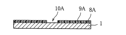
まず、図2で示したように、半絶縁性基板1の表面に、例えばプラズマCVD法で絶縁膜である例えばSiNx膜8Aを成膜して出発素材A0を製造する。
ついで、素材A0のSiNx膜8Aの表面にフォトレジスト9Aを塗布してパターニングしたのち、RIEのようなドライエッチング法でSiNx膜8Aを半絶縁性基板1の表面までエッチング除去して下部ゲート電極を形成すべき開口部10Aを形成し(図3)、更に、好適にはArのプラズマガスを用いたECRで、この開口部10Aから下部ゲート電極の材料を半絶縁性基板1の表出表面にスパッタリングしたのち、SiNx膜8Aを除去する。
【0018】
その結果、図4で示したように、半絶縁性基板1の所定箇所に下部ゲート電極2Aが設計基準のパターンで配線されている素材A1が得られる。
なお、この工程において、SiNx膜8Aに形成される開口部10Aは、最終的な製造目的である図1で示したGaN系FET(A)のゲート電極2Bのパターンと同じパターンで形成されることが必要である。
【0019】
ついで、素材A1の全面に再度プラズマCVD法でSiNx膜8Bを成膜し、更にフォトレジスト9Bを塗布してパターニングしたのち、RIEのようなドライエッチング法を行って図5で示した素材A2にする。この素材A2において、破線で示した部分8B,9Bが図1で示したGaN系FET(A)の活性層3を形成するための領域であり、実線で示した部分8B,9Bがコンタクト層4を形成するための領域である。
【0020】
ついで、素材A2の全面に所定のGaN系化合物半導体を選択成長させたのち、SiNx9Bを全てエッチング除去する。その結果、図6で示したように、活性層3で下部ゲート電極2Aが埋設されている素材A3が得られる。
ついで、図7で示したように、素材A3の全面にSiNx膜8Cを成膜し、更にその上にフォトレジスト9Cを塗布し、活性層3を被膜するSiNx膜8C(実線の部分)は残るようにパターニングしたのち、RIEのようなドライエッチング法を行って、破線の部分を除去することにより、半絶縁性基板1の表面と活性層3の側部を表出させる。
【0021】
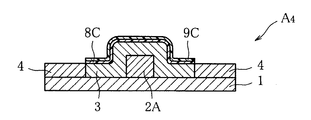
ついで、所定のGaN系化合物半導体の結晶成長を行い、図8で示したように、表出している上記箇所にコンタクト層4,4が形成されている素材A4を製造する。
そして、この素材A4のフォトレジスト9CとSiNx膜8Cをドライエッチング法で除去したのち、再び全面にSiNx膜8Dを保護膜として成膜し、更にフォトレジスト9Dを塗布し、ソース電極とドレイン電極を形成すべき箇所をドライエッチング法で除去し、そこにコンタクト層4,4の上面を表出させたのち、そこに電極材料を好適にはECRでスパッタリングしてソース電極5とドレイン電極6を形成し、図9で示した素材A5を製造する。
【0022】
ついで、フォトレジスト9Dを除去したのち、新たに素材A5の全面にフォトレジストを塗布し、活性層3の上に形成すべきゲート電極に対応する箇所をドライエッチング法で開口して上面3aを表出させたのちフォトレジストを除去し、図10で示した素材A6を製造する。
そして最後に、素材A6の全面にフォトレジストを塗布し、ゲート電極2Bを形成すべき箇所以外は全て残るようにパターニングしたのち、下部ゲート電極2Aと同一の材料を活性層3の上面3aに蒸着してゲート電極2Bを形成し、図1で示したGaN系FET(A)にする。
【0023】
本発明の別のGaN系FETの1例Bを図11に示す。
このGaN系FET(B)は、図1で示したGaN系FET(A)において活性層3が複数層(図では3層)から成る層3’で構成されているものである。
ここで、活性層3’の各層は、いずれも、GaN系化合物半導体で形成されているが、上・下層3A,3Aは同じ材料で構成され、中間層3Bは上・下層3A,3Aとは異なる材料で構成されることにより、全体としては、各層間はヘテロ接合界面を有する層構造になっている。具体的には、上・下層3A.3Aは例えばノンドープAlGaNで、中間層3BをノンドープGaNで形成することができる。
【0024】
また、上・下層3A,3AをノンドープGaNで、中間層3BをノンドープInGaNで構成してもよく、更には、上・下層3A,3AをノンドープAlInGaNAsPで、中間層3BをノンドープGaNAsPで構成してもよい。
この活性層3’の場合、下部ゲート電極2Aとゲート電極2Bの間に電圧を印加すると、活性層3’のヘテロ接合界面には2次元電子ガス層が発生する。
【0025】
その結果、チャネルの電子移動度は大きくなり、ソース電極5とドレイン電極6間には大きな電流が流れる。すなわち、オン抵抗が小さくなる。
【0026】
【実施例】
次のようにしてGaN系FET(A)を製造した。
まず、プラズマCVD法でサファイア基板1にSiNx膜8Aを成膜して図2で示した素材A0を製造した。ついで、SiNx膜8Aにフォトレジスト9Aを塗布したのちパターニングし、更にRIEでSiNx膜を除去して開口部10Aを形成した(図3)。
【0027】
ついで、Arのプラズマガスを用いたECR装置で、AuとPtを順次スパッタリングして開口部10Aに下部ゲート電極2Aを形成したのち、SiNx膜をHFでエッチング除去して、図4で示した素材A1を製造した。
素材A1の全面に、プラズマCVD法で再度SiNx膜8Bを成膜し、更にその上にフォトレジスト9Bを塗布して活性層3を形成すべき箇所をパターニングしたのち、RIEで開口して素材A2にした(図5)。
【0028】
ついで、素材A2に、窒素(3×10⁻⁶Torr),Ga(5×10⁻⁷Torr),Si(5×10⁻⁹Torr)を用い、成長温度850℃の分子線エピタキシャル成長法で、下部ゲート電極2Aを埋設する厚み1μmのn−GaN活性層3を形成したのち、SiNx膜を全てHFでエッチング除去し、図6で示した素材A3を製造した。なお、n−GaNから成る活性層3におけるSiのドーピング濃度は2×1017cm-3になっている。
【0029】
素材A3の全面に再びSiNx膜8Cを成膜し、更にその上にフォトレジスト9Cを塗布したのち、活性層3上のSiNx膜8Cは残るようにパターニングし、RIEで、コンタクト層を形成すべき箇所を開口してサファイア基板1の表面を表出させた(図7)。
ついで、分子線エピタキシャル成長法で、ラジカル窒素(3×10⁻⁶Torr),Ga(5×10⁻⁷Torr),Si(8×10⁻⁸Torr)を用い、成長温度850℃において、Siドープ−GaNから成る厚み1μmのコンタクト層4,4を形成して図8で示した素材A4を製造した。なお、コンタクト層4,4におけるSiのドーピング濃度は2×1019cm-3になっている。
【0030】
そして、フォトレジスト9CとSiNx膜8Cを全て除去したのち、全面に再びSiNx膜8Dを成膜し、更にフォトレジスト9Dを塗布したのちパターニングしてソース電極とドレイン電極を形成すべき箇所をRIEで開口し、そこにArのプラズマガスを用いたECRでAl,Ti,Auを順次スパッタしてソース電極5、ドレイン電極6を形成し、図9で示した素材A5を製造した。
【0031】
ついで、フォトレジスト9Dを除去したのち新たにフォトレジストを塗布してパターニングし、ゲート電極を形成すべき箇所をRIEで開口して活性層3の上面3aを表出させて図10で示した素材A6にした。
最後に、ソース電極とドレイン電極をマスクし、フォトレジストでパターニングして上部ゲート電極を形成すべき箇所を開口し、そこにArのプラズマガスを用いたECR蒸着でPt,Auを順次スパッタし、不要な部分に堆積したPt/Auを有機溶剤で除去してゲート電極を形成し、図1で示したMES−FETタイプのGaN系FET(A)を製造した。
【0032】
このMES−FETのソース−ドレイン間電圧は10Aで飽和した。また、耐圧は100Vを超えていた。そして、オン抵抗は10mΩcm-2以下であった。更に、このFETは、温度300℃においても動作した。
【0033】
【発明の効果】
以上の説明で明らかなように、本発明のGaN系FETは、オン抵抗が小さく、大電流スイッチング動作を実現することができる。そして同時に、活性層の上下にゲート電極を配置して活性層のチャネルを上下から挟むようなゲート部を形成することにより、ゲート部でのピンチオフ状態を容易に実現できる。
【図面の簡単な説明】
【図1】本発明のGaN系FETの1例Aを示す断面図である。
【図2】GaN系FET(A)の出発素材A0を示す断面図である。
【図3】下部ゲート電極の形成箇所を開口した状態を示す断面図である。
【図4】下部ゲート電極が形成された素材A1を示す断面図である。
【図5】素材A2を示す断面図である。
【図6】活性層3を形成した状態を示す断面図である。
【図7】コンタクト層の形成箇所を開口した状態を示す断面図である。
【図8】コンタクト層が形成された素材A4を示す断面図である。
【図9】活性層の上面が表出した状態の素材A5を示す断面図である。
【図10】ソース電極とドレイン電極が形成された素材A6を示す断面図である。
【図11】本発明の別のGaN系FETの1例Bを示す断面図である。
【符号の説明】
1 半絶縁性基板(サファイア基板)
2A 下部ゲート電極
2B ゲート電極
3,3’,3A,3B 活性層
3a 活性層3の上面
4 コンタクト層
5 ソース電極
6 ドレイン電極
7A,7B 空乏層
8A,8B,8C,8D 保護膜(SiNx膜)
9A,9B,9C,9D フォトレジスト
10A 開口部[0001]
BACKGROUND OF THE INVENTION
The present invention relates to a GaN-based field effect transistor (FET), and more particularly, a GaN-based structure having a novel structure useful as a switching element that has a low on-resistance, easily realizes a pinch-off state, and can operate at high temperature and drive a large current. It relates to FET.
[0002]
[Prior art]
Recently, research and development of FETs having a MIS (metal-insulating layer-semiconductor) structure are underway. In this case, GaAs-based compounds are the mainstream as compound semiconductors to be used.
The GaAs FET is generally manufactured as follows. First, a semi-insulating layer made of non-doped GaAs is formed on a substrate such as a sapphire substrate by MOCVD, for example, and an active layer made of Si-doped n-AlGaAs is further formed thereon. Then, an SiO 2 film is formed on the active layer by, for example, plasma CVD, and an opening having a desired pattern is formed by photolithography and etching, and a predetermined electrode material is formed from the opening. To form working electrodes such as a gate electrode, a source electrode, and a drain electrode on the active layer (Si-doped n-AlGaAs layer).
[0003]
By the way, with respect to recent FETs, for example, applications as switching elements mounted on automobiles are beginning to spread. For FETs in such fields of application, there is a demand for weight reduction and downsizing, as well as high temperature operation in consideration of the temperature in the engine room and high current drive. Yes. In relation to this latter requirement, the GaAs FET described above does not necessarily exhibit satisfactory characteristics.
[0004]
On the other hand, GaN-based compound semiconductors such as GaN, AlGaN, and InGaAlN can operate at a higher temperature than GaAs and Si, and the discontinuous band gap at the heterojunction interface is wide. When used as an active layer, it is possible to obtain an FET that can operate at a high temperature and can also apply a high voltage.
[0005]
For this reason, research and development of FETs using GaN-based compound semiconductors is underway, but the GaN-based FETs obtained so far are more active than conventional Si and GaAs-based FETs. Although there is an advantage that the on-resistance of the electrode is reduced by about one to three digits, there is still a considerable on-resistance due to the immaturity of the crystal growth technology and the electrode formation technology.
[0006]
In addition, even when a considerably high electric field is applied from the gate electrode to the active layer located immediately below the gate electrode, a depletion layer that completely shuts off the channel is not formed in the gate portion, so that a satisfactory pinch-off state is achieved. In some cases, a leakage current may flow between the source electrode and the drain electrode.
[0007]
[Problems to be solved by the invention]
The present invention solves the above-mentioned problems in the GaN-based FET, has a structure with a low on-resistance and easy to obtain a pinch-off state without generating a leakage current, and is designed to take full advantage of the characteristics of the GaN-based material. An object of the present invention is to provide a GaN-based FET.
[0008]
[Means for Solving the Problems]
In order to achieve the above object, in the present invention, a lower gate electrode made of the same material as the gate electrode to be formed is directly formed on the semi-insulating substrate in the same pattern as the gate electrode. The lower gate electrode is embedded to form at least one active layer made of a GaN-based compound semiconductor, the gate electrode is formed on the upper surface of the active layer, and the gate electrodes are vertically arranged with the active layer interposed therebetween. A GaN-based field effect transistor is provided.
[0009]
DETAILED DESCRIPTION OF THE INVENTION
A basic configuration A of the GaN-based FET of the present invention is shown in FIG.
In this GaN-based FET (A), a
[0010]
Here, the
[0011]
Then,
In the case of this FET (A), the gate portion G is composed of the
[0012]
Therefore, even if the channel of the
This means that in the case of the FET (A), the pinch-off state can be realized more easily in comparison with the conventional FET trying to realize the pinch-off state with one gate electrode. means.
[0013]
In the FET (A) shown in FIG. 1, as the
Both the
[0014]
The
[0015]
The
Examples of the GaN compound semiconductor used include GaN, AlGaN, InGaN, AlInGaN, InGaNAs, InGaNP, and the like.
[0016]
In the case of the GaN-based FET (A), when the
Next, the
[0017]
The GaN-based FET (A) of the present invention can be manufactured as follows. The manufacturing method will be described in the order of steps with reference to the drawings.
First, as shown in FIG. 2, the semi-insulating surface of the
Then, after patterning a photoresist is applied 9A on the surface of the SiN x film 8A of the material A 0, lower the the SiN x film 8A in dry etching is removed by etching to the semi-insulating surface of the
[0018]
As a result, as shown in FIG. 4, a material A 1 is obtained in which the
In this step, the
[0019]
Next, an SiN x film 8B is again formed on the entire surface of the material A 1 by plasma CVD, and after further applying and patterning a
[0020]
Next, after a predetermined GaN compound semiconductor is selectively grown on the entire surface of the material A 2 , all the
Next, as shown in FIG. 7, a SiN x film 8C is formed on the entire surface of the material A 3, a
[0021]
Next, crystal growth of a predetermined GaN-based compound semiconductor is performed, and as shown in FIG. 8, a material A 4 in which the contact layers 4 and 4 are formed at the exposed positions is manufactured.
Then, after removing the
[0022]
Then, after removing the
Finally, a photoresist is applied to the entire surface of the material A 6 and patterned so as to remain except for the portion where the
[0023]
FIG. 11 shows an example B of another GaN-based FET of the present invention.
In this GaN-based FET (B), the
Here, each layer of the
[0024]
The upper and
In the case of this
[0025]
As a result, the electron mobility of the channel increases, and a large current flows between the
[0026]
【Example】
A GaN-based FET (A) was manufactured as follows.
First, it was prepared material A 0 shown in FIG. 2 by forming a the SiN x film 8A the
[0027]
Next, Au and Pt were sequentially sputtered by an ECR apparatus using Ar plasma gas to form the
An SiN x film 8B is formed again on the entire surface of the material A 1 by plasma CVD, and a
[0028]
Next, the material A 2 is nitrogen (3 × 10 −6 Torr), Ga (5 × 10 −7 Torr), Si (5 × 10 −9 Torr), and is grown by molecular beam epitaxy at a growth temperature of 850 ° C. After forming the n-GaN
[0029]
An SiN x film 8C is formed again on the entire surface of the material A 3 , and further, a
Next, in the molecular beam epitaxial growth method, radical nitrogen (3 × 10 −6 Torr), Ga (5 × 10 −7 Torr), Si (8 × 10 −8 Torr) is used, and Si is doped at a growth temperature of 850 ° C. Contact layers 4 and 4 made of GaN having a thickness of 1 μm were formed to manufacture the material A 4 shown in FIG. The Si doping concentration in the contact layers 4 and 4 is 2 × 10 19 cm −3 .
[0030]
Then, after removing all of the
[0031]
Next, after removing the
Finally, the source electrode and the drain electrode are masked, patterned with a photoresist to open a portion where an upper gate electrode is to be formed, and Pt and Au are sequentially sputtered there by ECR deposition using Ar plasma gas, Pt / Au deposited on unnecessary portions was removed with an organic solvent to form a gate electrode, and the MES-FET type GaN-based FET (A) shown in FIG. 1 was manufactured.
[0032]
The source-drain voltage of this MES-FET was saturated at 10A. Moreover, the withstand voltage exceeded 100V. The on-resistance was 10 mΩcm −2 or less. Furthermore, this FET operated even at a temperature of 300 ° C.
[0033]
【The invention's effect】
As is clear from the above description, the GaN-based FET of the present invention has a low on-resistance and can realize a large current switching operation. At the same time, the gate electrodes are arranged above and below the active layer to form a gate portion that sandwiches the channel of the active layer from above and below, so that a pinch-off state at the gate portion can be easily realized.
[Brief description of the drawings]
FIG. 1 is a cross-sectional view showing an example A of a GaN-based FET of the present invention.
FIG. 2 is a cross-sectional view showing a starting material A 0 of a GaN-based FET (A).
FIG. 3 is a cross-sectional view showing a state in which a formation portion of a lower gate electrode is opened.
FIG. 4 is a cross-sectional view showing a material A 1 on which a lower gate electrode is formed.
FIG. 5 is a cross-sectional view showing a material A 2 ;
FIG. 6 is a cross-sectional view showing a state in which an
FIG. 7 is a cross-sectional view showing a state in which a contact layer formation portion is opened.
FIG. 8 is a cross-sectional view showing a material A 4 on which a contact layer is formed.
FIG. 9 is a cross-sectional view showing the material A 5 with the upper surface of the active layer exposed.
FIG. 10 is a cross-sectional view showing a material A 6 on which a source electrode and a drain electrode are formed.
FIG. 11 is a cross-sectional view showing an example B of another GaN-based FET of the present invention.
[Explanation of symbols]
1 Semi-insulating substrate (sapphire substrate)
2A
9A, 9B, 9C,
Claims (2)
前記下部ゲート電極を埋設して前記下部ゲート電極の側面および上面に接する下部GaN系化合物半導体から成る少なくとも1層の活性層が形成され、
前記活性層の上面には前記ゲート電極が形成され、
前記活性層を挟んで上下にゲート電極が配置されていることを特徴とするGaN系電界効果トランジスタ。On the semi-insulating substrate, a lower gate electrode made of the same material as the gate electrode to be formed is directly formed on the surface of the semi-insulating substrate in the same pattern as the gate electrode,
At least one active layer made of a lower GaN-based compound semiconductor is formed by burying the lower gate electrode and in contact with a side surface and an upper surface of the lower gate electrode ,
The gate electrode is formed on the upper surface of the active layer,
A GaN-based field effect transistor, wherein gate electrodes are arranged above and below the active layer.
Priority Applications (2)
| Application Number | Priority Date | Filing Date | Title |
|---|---|---|---|
| JP2001062323A JP4804635B2 (en) | 2001-03-06 | 2001-03-06 | GaN-based field effect transistor |
| US10/084,717 US6576927B2 (en) | 2001-03-06 | 2002-02-25 | Semiconductor device and GaN-based field effect transistor for use in the same |
Applications Claiming Priority (1)
| Application Number | Priority Date | Filing Date | Title |
|---|---|---|---|
| JP2001062323A JP4804635B2 (en) | 2001-03-06 | 2001-03-06 | GaN-based field effect transistor |
Publications (2)
| Publication Number | Publication Date |
|---|---|
| JP2002270618A JP2002270618A (en) | 2002-09-20 |
| JP4804635B2 true JP4804635B2 (en) | 2011-11-02 |
Family
ID=18921481
Family Applications (1)
| Application Number | Title | Priority Date | Filing Date |
|---|---|---|---|
| JP2001062323A Expired - Lifetime JP4804635B2 (en) | 2001-03-06 | 2001-03-06 | GaN-based field effect transistor |
Country Status (1)
| Country | Link |
|---|---|
| JP (1) | JP4804635B2 (en) |
Families Citing this family (4)
| Publication number | Priority date | Publication date | Assignee | Title |
|---|---|---|---|---|
| JP4142429B2 (en) * | 2002-12-26 | 2008-09-03 | 古河電気工業株式会社 | Current detection circuit |
| US7088431B2 (en) * | 2003-12-17 | 2006-08-08 | Asml Netherlands B.V. | Lithographic apparatus and device manufacturing method |
| JP2012049170A (en) * | 2010-08-24 | 2012-03-08 | New Japan Radio Co Ltd | Nitride semiconductor device |
| WO2013005372A1 (en) * | 2011-07-01 | 2013-01-10 | パナソニック株式会社 | Semiconductor device |
Family Cites Families (6)
| Publication number | Priority date | Publication date | Assignee | Title |
|---|---|---|---|---|
| JPS60229375A (en) * | 1984-04-26 | 1985-11-14 | Sony Corp | Manufacture of compound semiconductor device |
| JPH02111036A (en) * | 1988-10-20 | 1990-04-24 | Fujitsu Ltd | High-mobility transistor |
| JPH05129338A (en) * | 1991-11-01 | 1993-05-25 | Hitachi Ltd | Field-effect transistor and its manufacture |
| JPH0982940A (en) * | 1995-09-14 | 1997-03-28 | Hitachi Ltd | Semiconductor device and manufacturing method thereof |
| JPH0982966A (en) * | 1995-09-19 | 1997-03-28 | Sony Corp | Semiconductor device and double-sided gate thin film transistor manufacturing method |
| JP2000082671A (en) * | 1998-06-26 | 2000-03-21 | Sony Corp | Nitride III-V compound semiconductor device and method of manufacturing the same |
-
2001
- 2001-03-06 JP JP2001062323A patent/JP4804635B2/en not_active Expired - Lifetime
Also Published As
| Publication number | Publication date |
|---|---|
| JP2002270618A (en) | 2002-09-20 |
Similar Documents
| Publication | Publication Date | Title |
|---|---|---|
| JP5160225B2 (en) | Method for fabricating nitride-based transistor with regrowth ohmic contact region and nitride-based transistor with regrowth ohmic contact region | |
| EP2065925B1 (en) | Field-effect transistor | |
| US6593193B2 (en) | Semiconductor device and method for fabricating the same | |
| KR101108344B1 (en) | Methods of fabricating nitride-based transistors with a cap layer and a recessed gate | |
| JP4190754B2 (en) | Method for manufacturing field effect transistor | |
| US20080176366A1 (en) | Method for fabricating AIGaN/GaN-HEMT using selective regrowth | |
| KR101092467B1 (en) | Enhancement normally off nitride semiconductor device and manufacturing method thereof | |
| US11335797B2 (en) | Semiconductor devices and methods for fabricating the same | |
| JP2013520014A (en) | Contact structure comprising alternating layers of metal and silicon and method of forming related devices | |
| JP2014011350A (en) | Method of manufacturing semiconductor device | |
| JP2011238931A (en) | Enhancement mode field effect device and method of manufacturing the same | |
| US20220376074A1 (en) | Nitride-based semiconductor device and method for manufacturing the same | |
| JP4906023B2 (en) | GaN-based semiconductor device | |
| US7465968B2 (en) | Semiconductor device and method for fabricating the same | |
| JP5101143B2 (en) | Field effect transistor and manufacturing method thereof | |
| JP2000208760A (en) | Field effect transistor | |
| JP3984471B2 (en) | Semiconductor device and manufacturing method thereof | |
| JP4804635B2 (en) | GaN-based field effect transistor | |
| US6576927B2 (en) | Semiconductor device and GaN-based field effect transistor for use in the same | |
| TWI726282B (en) | Semiconductor devices and methods for fabricating the same | |
| JP2003197645A (en) | Heterojunction field effect transistor and method of manufacturing the same | |
| JP4955858B2 (en) | Multi-layer semiconductor device | |
| JP2015130374A (en) | Method for manufacturing nitride semiconductor device | |
| JP2007207820A (en) | Field effect transistor and manufacturing method thereof | |
| KR100985470B1 (en) | High electron mobility transistor and manufacturing method |
Legal Events
| Date | Code | Title | Description |
|---|---|---|---|
| RD05 | Notification of revocation of power of attorney |
Free format text: JAPANESE INTERMEDIATE CODE: A7425 Effective date: 20050922 |
|
| A621 | Written request for application examination |
Free format text: JAPANESE INTERMEDIATE CODE: A621 Effective date: 20071203 |
|
| A977 | Report on retrieval |
Free format text: JAPANESE INTERMEDIATE CODE: A971007 Effective date: 20110426 |
|
| A131 | Notification of reasons for refusal |
Free format text: JAPANESE INTERMEDIATE CODE: A131 Effective date: 20110509 |
|
| A521 | Written amendment |
Free format text: JAPANESE INTERMEDIATE CODE: A523 Effective date: 20110707 |
|
| RD02 | Notification of acceptance of power of attorney |
Free format text: JAPANESE INTERMEDIATE CODE: A7422 Effective date: 20110707 |
|
| TRDD | Decision of grant or rejection written | ||
| A01 | Written decision to grant a patent or to grant a registration (utility model) |
Free format text: JAPANESE INTERMEDIATE CODE: A01 Effective date: 20110726 |
|
| A01 | Written decision to grant a patent or to grant a registration (utility model) |
Free format text: JAPANESE INTERMEDIATE CODE: A01 |
|
| A61 | First payment of annual fees (during grant procedure) |
Free format text: JAPANESE INTERMEDIATE CODE: A61 Effective date: 20110810 |
|
| R151 | Written notification of patent or utility model registration |
Ref document number: 4804635 Country of ref document: JP Free format text: JAPANESE INTERMEDIATE CODE: R151 |
|
| FPAY | Renewal fee payment (event date is renewal date of database) |
Free format text: PAYMENT UNTIL: 20140819 Year of fee payment: 3 |
|
| EXPY | Cancellation because of completion of term |