JP4803836B2 - 撮像光学系 - Google Patents
撮像光学系 Download PDFInfo
- Publication number
- JP4803836B2 JP4803836B2 JP2007529551A JP2007529551A JP4803836B2 JP 4803836 B2 JP4803836 B2 JP 4803836B2 JP 2007529551 A JP2007529551 A JP 2007529551A JP 2007529551 A JP2007529551 A JP 2007529551A JP 4803836 B2 JP4803836 B2 JP 4803836B2
- Authority
- JP
- Japan
- Prior art keywords
- antireflection
- lens element
- optical surface
- optical system
- imaging optical
- Prior art date
- Legal status (The legal status is an assumption and is not a legal conclusion. Google has not performed a legal analysis and makes no representation as to the accuracy of the status listed.)
- Expired - Fee Related
Links
Images


Classifications
-
- G—PHYSICS
- G02—OPTICS
- G02B—OPTICAL ELEMENTS, SYSTEMS OR APPARATUS
- G02B1/00—Optical elements characterised by the material of which they are made; Optical coatings for optical elements
- G02B1/10—Optical coatings produced by application to, or surface treatment of, optical elements
- G02B1/11—Anti-reflection coatings
- G02B1/118—Anti-reflection coatings having sub-optical wavelength surface structures designed to provide an enhanced transmittance, e.g. moth-eye structures
-
- G—PHYSICS
- G02—OPTICS
- G02B—OPTICAL ELEMENTS, SYSTEMS OR APPARATUS
- G02B1/00—Optical elements characterised by the material of which they are made; Optical coatings for optical elements
- G02B1/10—Optical coatings produced by application to, or surface treatment of, optical elements
- G02B1/11—Anti-reflection coatings
-
- G—PHYSICS
- G02—OPTICS
- G02B—OPTICAL ELEMENTS, SYSTEMS OR APPARATUS
- G02B3/00—Simple or compound lenses
- G02B3/0006—Arrays
- G02B3/0037—Arrays characterized by the distribution or form of lenses
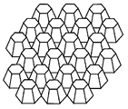
- G02B3/0056—Arrays characterized by the distribution or form of lenses arranged along two different directions in a plane, e.g. honeycomb arrangement of lenses
-
- G—PHYSICS
- G02—OPTICS
- G02B—OPTICAL ELEMENTS, SYSTEMS OR APPARATUS
- G02B3/00—Simple or compound lenses
- G02B3/0006—Arrays
-
- G—PHYSICS
- G02—OPTICS
- G02B—OPTICAL ELEMENTS, SYSTEMS OR APPARATUS
- G02B5/00—Optical elements other than lenses
- G02B5/001—Axicons, waxicons, reflaxicons
-
- G—PHYSICS
- G02—OPTICS
- G02B—OPTICAL ELEMENTS, SYSTEMS OR APPARATUS
- G02B5/00—Optical elements other than lenses
- G02B5/04—Prisms
- G02B5/045—Prism arrays
Description
少なくとも1つのレンズ素子を備える撮像光学系であって、
入射光が透過する光学面と、
反射防止構造体とを備え、
前記反射防止構造体が、1つ以上の曲率を有する光学面において、該光学面の中心を含む中心領域には設けられず、該中心領域の周辺に位置する周辺領域の少なくとも一部に設けられており、
少なくとも前記光学面の前記中心領域の一部に、反射防止機能を有する反射防止多層膜が形成されており、
前記周辺領域が、光学有効径内にあり、
前記反射防止構造体が、前記入射光中の、反射を防止すべき光の最短波長よりも小さいピッチで、所定の形状を有する構造単位が周期的にアレイ状に配列された構造体であり、
前記周辺領域と前記中心領域との境界が、以下の条件(1):
RD×0.20<BR<RD×0.70 ・・・(1)
(ここで、
RD:光学面の曲率半径、
BR:光軸から周辺領域と中心領域との境界までの半径方向の距離
である)
を満足する、撮像光学系
に関する。
図1は、実施の形態1に係る撮像光学系1の構成を示す概略断面図である。図1は、焦点距離が変動しない広角撮影に適した撮像光学系の例を示しており、撮像光学系1は、鏡筒6に保持されている。光束5a、5b及び5cは、撮像光学系1を通過する光束であり、光束5cは、撮像光学系1の最大画角を通過する光束である。
RD×0.20<BR<RD×0.70 ・・・(1)
ここで、
RD:光学面の曲率半径、
BR:光軸から周辺領域と中心領域との境界までの半径方向の距離
である。なお、該条件(1)は、曲率を有する光学面に対して成立するものである。
RD×0.25<BR ・・・(1a)
ここで、
RD:光学面の曲率半径、
BR:光軸から周辺領域と中心領域との境界までの半径方向の距離
である。RD×0.25は、入射角度が約17.5°となる値である。該条件(1a)を満足することにより、レンズ素子を保持するためのスペースを充分に確保しつつ、反射防止構造体によってさらに高い反射防止効果を得ることができる。
RD×0.40<BR<RD×0.60 ・・・(1b)
ここで、
RD:光学面の曲率半径、
BR:光軸から周辺領域と中心領域との境界までの半径方向の距離
である。
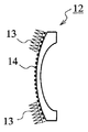
実施の形態1では、反射防止多層膜が最物体側に位置するレンズ素子の中心領域に形成され、周辺領域に反射防止構造体が形成されている。ここで、反射防止多層膜をレンズ素子の表面全体を覆うように形成し、その上に反射防止構造体を形成することもできる。
本実施の形態3に係る撮像光学系の基本構成は、実施の形態1に係る撮像光学系と同様であるが、最物体側に位置するレンズ素子において、その物体側の光学面の周辺領域の少なくも一部に設けられた反射防止構造体の構成が、実施の形態1における反射防止構造体の構成と相違する。
本実施例の撮像光学系は、図1に示す実施の形態1に係る撮像光学系に対応する。図12は、本実施例において、撮像光学系に含まれるレンズ素子のうち、最物体側に位置するレンズ素子の物体側の光学面に形成された反射防止構造体を示す概略拡大図である。図12に示す反射防止構造体は、高さ約300nmの四角錐形状を有する構造単位が、ピッチ約100nmで周期的にアレイ状に配置された構造体である。また、反射防止構造体を構成する基材は、BK7である。
参考文献1:M.G.Moharam and T.K.Gaylord;“Rigorous coupled−wave analysis of planar−grating diffraction”,J.Opt.Soc.Am.71(1981)811−818(エム・ジー・モハラム及びティー・ケイ・ゲイロードによる「リガラス カプルドウェーブ アナリシス オブ プラナーグレイティング ディフラクション」ジャーナル オブ ザ オプティカル ソサイエティ オブ アメリカ 第71巻(1981年)811〜818頁)
参考文献2:M.G.Moharam;“Coupled−Wave Analysis of Two Dimensional Dielectric Gratings”,SPIE−The International Society for Optical Engineering 883(1988)8−11(エム・ジー・モハラムによる「カプルドウェーブ アナリシス オブ トゥー ディメンジョナル ジエレクトリック グレイティングス」エス・ピー・アイ・イー−ジ インターナショナル ソサイエティ フォー オプティカル エンジニアリング 第883巻(1988年)8〜11頁)
2、12、22 最物体側に位置するレンズ素子
3、13、23 反射防止構造体
4、14 反射防止多層膜
5a、5b、5c 光束
6 鏡筒
24 基材
25 シート
Claims (4)
- 少なくとも1つのレンズ素子を備える撮像光学系であって、
入射光が透過する光学面と、
反射防止構造体とを備え、
前記反射防止構造体が、1つ以上の曲率を有する光学面において、該光学面の中心を含む中心領域には設けられず、該中心領域の周辺に位置する周辺領域の少なくとも一部に設けられており、
少なくとも前記光学面の前記中心領域の一部に、反射防止機能を有する反射防止多層膜が形成されており、
前記周辺領域が、光学有効径内にあり、
前記反射防止構造体が、前記入射光中の、反射を防止すべき光の最短波長よりも小さいピッチで、所定の形状を有する構造単位が周期的にアレイ状に配列された構造体であり、
前記周辺領域と前記中心領域との境界が、以下の条件(1):
RD×0.20<BR<RD×0.70 ・・・(1)
(ここで、
RD:光学面の曲率半径、
BR:光軸から周辺領域と中心領域との境界までの半径方向の距離
である)
を満足する、撮像光学系。 - 多層膜と反射防止構造体とが、互いに部分的に重畳する、請求項1に記載の撮像光学系。
- 反射防止構造体が、樹脂材料にて形成されている、請求項1に記載の撮像光学系。
- 反射防止構造体を有する光学面が、最物体側に位置するレンズ素子の物体側の光学面である、請求項1に記載の撮像光学系。
Priority Applications (1)
| Application Number | Priority Date | Filing Date | Title |
|---|---|---|---|
| JP2007529551A JP4803836B2 (ja) | 2005-08-08 | 2006-08-04 | 撮像光学系 |
Applications Claiming Priority (4)
| Application Number | Priority Date | Filing Date | Title |
|---|---|---|---|
| JP2005229161 | 2005-08-08 | ||
| JP2005229161 | 2005-08-08 | ||
| PCT/JP2006/315510 WO2007018149A1 (ja) | 2005-08-08 | 2006-08-04 | 撮像光学系 |
| JP2007529551A JP4803836B2 (ja) | 2005-08-08 | 2006-08-04 | 撮像光学系 |
Publications (2)
| Publication Number | Publication Date |
|---|---|
| JPWO2007018149A1 JPWO2007018149A1 (ja) | 2009-02-19 |
| JP4803836B2 true JP4803836B2 (ja) | 2011-10-26 |
Family
ID=37727332
Family Applications (1)
| Application Number | Title | Priority Date | Filing Date |
|---|---|---|---|
| JP2007529551A Expired - Fee Related JP4803836B2 (ja) | 2005-08-08 | 2006-08-04 | 撮像光学系 |
Country Status (4)
| Country | Link |
|---|---|
| US (1) | US20090257127A1 (ja) |
| JP (1) | JP4803836B2 (ja) |
| CN (1) | CN101233429B (ja) |
| WO (1) | WO2007018149A1 (ja) |
Families Citing this family (19)
| Publication number | Priority date | Publication date | Assignee | Title |
|---|---|---|---|---|
| GB0712605D0 (en) * | 2007-06-28 | 2007-08-08 | Microsharp Corp Ltd | Optical film |
| JP2009042472A (ja) * | 2007-08-08 | 2009-02-26 | Canon Inc | 光学素子 |
| JP5213424B2 (ja) * | 2007-12-10 | 2013-06-19 | キヤノン株式会社 | 光学系及びそれを有する光学機器 |
| GB2465607A (en) * | 2008-11-25 | 2010-05-26 | St Microelectronics | CMOS imager structures |
| JP5522955B2 (ja) * | 2009-02-17 | 2014-06-18 | キヤノン株式会社 | 光学素子の製造方法 |
| JP2011053496A (ja) * | 2009-09-02 | 2011-03-17 | Sony Corp | 光学素子およびその製造方法、ならびに原盤の製造方法 |
| JP2011053495A (ja) * | 2009-09-02 | 2011-03-17 | Sony Corp | 光学素子、およびその製造方法 |
| JP5352010B2 (ja) * | 2011-02-22 | 2013-11-27 | パナソニック株式会社 | 光学部材 |
| JP2015018005A (ja) * | 2011-11-11 | 2015-01-29 | パナソニック株式会社 | レンズ鏡筒 |
| JP5525656B2 (ja) * | 2012-02-06 | 2014-06-18 | パナソニック株式会社 | 光学素子の製造方法 |
| JP5376029B1 (ja) * | 2012-09-28 | 2013-12-25 | 大日本印刷株式会社 | 反射防止物品 |
| US8442792B1 (en) * | 2012-10-26 | 2013-05-14 | Elbex Video Ltd. | Method and apparatus for calibrating intelligent AC outlets |
| US10197800B2 (en) * | 2015-09-25 | 2019-02-05 | Everready Precision Ind. Corp. | Optical lens |
| JP6786248B2 (ja) * | 2016-04-12 | 2020-11-18 | キヤノン株式会社 | 光学素子およびその製造方法 |
| JP2018077304A (ja) * | 2016-11-08 | 2018-05-17 | 株式会社デンソー | 撮像装置 |
| JP7296696B2 (ja) * | 2017-12-25 | 2023-06-23 | マクセル株式会社 | 広角レンズユニットおよびカメラモジュール |
| US11485052B2 (en) | 2018-07-30 | 2022-11-01 | Canon Kabushiki Kaisha | Resin product, method of making resin product, interchangeable lens, and optical device |
| JP2020112747A (ja) * | 2019-01-16 | 2020-07-27 | 株式会社タムロン | 光学素子及びその製造方法 |
| KR20220022303A (ko) | 2020-08-18 | 2022-02-25 | 삼성전기주식회사 | 카메라 모듈 및 휴대 단말기 |
Citations (3)
| Publication number | Priority date | Publication date | Assignee | Title |
|---|---|---|---|---|
| JP2003329806A (ja) * | 2002-05-10 | 2003-11-19 | Canon Inc | 光学機器 |
| JP2005148591A (ja) * | 2003-11-19 | 2005-06-09 | Olympus Corp | 反射光学素子 |
| JP2005157119A (ja) * | 2003-11-27 | 2005-06-16 | Olympus Corp | 反射防止光学素子及びこれを用いた光学系 |
Family Cites Families (12)
| Publication number | Priority date | Publication date | Assignee | Title |
|---|---|---|---|---|
| JPH10161020A (ja) * | 1996-12-02 | 1998-06-19 | Olympus Optical Co Ltd | 回折光学素子を用いた撮影光学系 |
| JPH10186102A (ja) * | 1996-12-26 | 1998-07-14 | Yazaki Corp | 反射防止膜 |
| JP2004513483A (ja) * | 2000-11-02 | 2004-04-30 | スリーエム イノベイティブ プロパティズ カンパニー | 明るさおよびコントラスト増強直視型発光型ディスプレイ |
| EP1412782A4 (en) * | 2000-11-03 | 2006-02-15 | Mems Optical Inc | ANTI-REFLECTIVE STRUCTURES |
| JP4848583B2 (ja) * | 2000-11-21 | 2011-12-28 | 大日本印刷株式会社 | ハードコート層を有するフィルムの製造方法 |
| JP2002350624A (ja) * | 2001-05-25 | 2002-12-04 | Canon Inc | 光学素子及びそれを有する走査光学系及び画像形成装置 |
| JP2003004916A (ja) * | 2001-06-20 | 2003-01-08 | Dainippon Printing Co Ltd | 表示装置の窓材、その製造方法、及び表示装置 |
| JP4018440B2 (ja) * | 2002-05-07 | 2007-12-05 | キヤノン株式会社 | 観察光学系および光学機器 |
| TW200502670A (en) * | 2002-11-21 | 2005-01-16 | Konica Minolta Holdings Inc | Objective lens, optical system and optical pickup apparatus |
| US7212340B2 (en) * | 2003-07-14 | 2007-05-01 | Konica Minolta Holdings, Inc. | Forming methods, forming devices for articles having a micro-sized shape and optical elements |
| JP2005062526A (ja) * | 2003-08-13 | 2005-03-10 | Canon Inc | 光学素子および光学系 |
| JP4833569B2 (ja) * | 2005-03-24 | 2011-12-07 | パナソニック株式会社 | 反射防止構造を有する光学レンズ |
-
2006
- 2006-08-04 JP JP2007529551A patent/JP4803836B2/ja not_active Expired - Fee Related
- 2006-08-04 US US12/063,147 patent/US20090257127A1/en not_active Abandoned
- 2006-08-04 CN CN2006800284401A patent/CN101233429B/zh not_active Expired - Fee Related
- 2006-08-04 WO PCT/JP2006/315510 patent/WO2007018149A1/ja active Application Filing
Patent Citations (3)
| Publication number | Priority date | Publication date | Assignee | Title |
|---|---|---|---|---|
| JP2003329806A (ja) * | 2002-05-10 | 2003-11-19 | Canon Inc | 光学機器 |
| JP2005148591A (ja) * | 2003-11-19 | 2005-06-09 | Olympus Corp | 反射光学素子 |
| JP2005157119A (ja) * | 2003-11-27 | 2005-06-16 | Olympus Corp | 反射防止光学素子及びこれを用いた光学系 |
Also Published As
| Publication number | Publication date |
|---|---|
| CN101233429A (zh) | 2008-07-30 |
| US20090257127A1 (en) | 2009-10-15 |
| JPWO2007018149A1 (ja) | 2009-02-19 |
| CN101233429B (zh) | 2011-06-15 |
| WO2007018149A1 (ja) | 2007-02-15 |
Similar Documents
| Publication | Publication Date | Title |
|---|---|---|
| JP4803836B2 (ja) | 撮像光学系 | |
| JP4608501B2 (ja) | 光吸収部材及びそれからなるレンズ鏡筒 | |
| JP5512269B2 (ja) | 反射防止構造体、光学ユニット及び光学装置 | |
| JP4587418B2 (ja) | 回折光学素子及び該回折光学素子を有する光学系 | |
| JP2005157119A (ja) | 反射防止光学素子及びこれを用いた光学系 | |
| JP2008276059A (ja) | 光学素子およびそれを有する光学系 | |
| WO2008001662A1 (fr) | Élément optique et dispositif optique le comprenant | |
| JP2006267624A (ja) | 反射防止構造を有する光学レンズ | |
| JP5854628B2 (ja) | 光学系、およびそれを用いた光学機器 | |
| JP2005062526A (ja) | 光学素子および光学系 | |
| JP2010271533A (ja) | 光学素子及びそれを有する光学系 | |
| JP6783829B2 (ja) | 回折光学素子およびそれを用いた光学機器 | |
| JP2007171857A (ja) | 光学素子および光走査装置 | |
| JP5014339B2 (ja) | 光学部材 | |
| JP5031496B2 (ja) | 光学系及びそれを有する撮像装置 | |
| JP5213424B2 (ja) | 光学系及びそれを有する光学機器 | |
| JP5986454B2 (ja) | レンズ装置及びそれを有する撮像装置 | |
| JP5676930B2 (ja) | 回折光学素子、光学系および光学機器 | |
| JP2004361906A (ja) | 透過型光学素子および光学装置 | |
| TW202331393A (zh) | 成像鏡頭及電子裝置 | |
| JP2015028552A (ja) | 光学素子およびその製造方法 | |
| JP2007206490A (ja) | 複合型光学素子および光学系 | |
| JP2007298918A (ja) | 光学素子及びそれを有する光学系 | |
| JP5414945B1 (ja) | 光学素子及びそれを備えた撮像装置 | |
| JP2017134362A (ja) | 光学素子及びそれを有する光学系 |
Legal Events
| Date | Code | Title | Description |
|---|---|---|---|
| A131 | Notification of reasons for refusal |
Free format text: JAPANESE INTERMEDIATE CODE: A131 Effective date: 20110317 |
|
| A521 | Written amendment |
Free format text: JAPANESE INTERMEDIATE CODE: A523 Effective date: 20110512 |
|
| A131 | Notification of reasons for refusal |
Free format text: JAPANESE INTERMEDIATE CODE: A131 Effective date: 20110601 |
|
| A521 | Written amendment |
Free format text: JAPANESE INTERMEDIATE CODE: A523 Effective date: 20110708 |
|
| TRDD | Decision of grant or rejection written | ||
| A01 | Written decision to grant a patent or to grant a registration (utility model) |
Free format text: JAPANESE INTERMEDIATE CODE: A01 Effective date: 20110804 |
|
| A01 | Written decision to grant a patent or to grant a registration (utility model) |
Free format text: JAPANESE INTERMEDIATE CODE: A01 |
|
| A61 | First payment of annual fees (during grant procedure) |
Free format text: JAPANESE INTERMEDIATE CODE: A61 Effective date: 20110808 |
|
| R150 | Certificate of patent or registration of utility model |
Free format text: JAPANESE INTERMEDIATE CODE: R150 |
|
| FPAY | Renewal fee payment (event date is renewal date of database) |
Free format text: PAYMENT UNTIL: 20140819 Year of fee payment: 3 |
|
| RD02 | Notification of acceptance of power of attorney |
Free format text: JAPANESE INTERMEDIATE CODE: A7422 Effective date: 20110826 |
|
| LAPS | Cancellation because of no payment of annual fees |