JP4780765B2 - 連結検出器ピクセル、光子/パルスカウント輻射線像形成素子 - Google Patents
連結検出器ピクセル、光子/パルスカウント輻射線像形成素子 Download PDFInfo
- Publication number
- JP4780765B2 JP4780765B2 JP2005512631A JP2005512631A JP4780765B2 JP 4780765 B2 JP4780765 B2 JP 4780765B2 JP 2005512631 A JP2005512631 A JP 2005512631A JP 2005512631 A JP2005512631 A JP 2005512631A JP 4780765 B2 JP4780765 B2 JP 4780765B2
- Authority
- JP
- Japan
- Prior art keywords
- pixel
- detector
- circuit
- ray
- pixel signal
- Prior art date
- Legal status (The legal status is an assumption and is not a legal conclusion. Google has not performed a legal analysis and makes no representation as to the accuracy of the status listed.)
- Expired - Fee Related
Links
- 238000003384 imaging method Methods 0.000 title claims description 50
- 230000005855 radiation Effects 0.000 title claims description 49
- 239000000758 substrate Substances 0.000 claims description 76
- 239000004065 semiconductor Substances 0.000 claims description 52
- 238000004891 communication Methods 0.000 claims description 34
- 230000003750 conditioning effect Effects 0.000 claims description 17
- 238000012545 processing Methods 0.000 claims description 16
- 230000008878 coupling Effects 0.000 claims description 15
- 238000010168 coupling process Methods 0.000 claims description 15
- 238000005859 coupling reaction Methods 0.000 claims description 15
- 230000005251 gamma ray Effects 0.000 claims description 12
- 230000003321 amplification Effects 0.000 claims description 4
- 238000003199 nucleic acid amplification method Methods 0.000 claims description 4
- 238000003079 width control Methods 0.000 claims description 4
- 229910000679 solder Inorganic materials 0.000 claims description 2
- 239000000463 material Substances 0.000 description 16
- 238000010586 diagram Methods 0.000 description 10
- 230000001143 conditioned effect Effects 0.000 description 6
- 238000001514 detection method Methods 0.000 description 6
- 230000000694 effects Effects 0.000 description 6
- 230000008901 benefit Effects 0.000 description 4
- 238000005516 engineering process Methods 0.000 description 4
- 229910004613 CdTe Inorganic materials 0.000 description 3
- 238000000034 method Methods 0.000 description 3
- 230000004044 response Effects 0.000 description 3
- 238000007493 shaping process Methods 0.000 description 3
- 229910004611 CdZnTe Inorganic materials 0.000 description 2
- 238000010521 absorption reaction Methods 0.000 description 2
- 230000009286 beneficial effect Effects 0.000 description 2
- 230000005684 electric field Effects 0.000 description 2
- 238000009206 nuclear medicine Methods 0.000 description 2
- 230000008569 process Effects 0.000 description 2
- 229910001218 Gallium arsenide Inorganic materials 0.000 description 1
- 229910000661 Mercury cadmium telluride Inorganic materials 0.000 description 1
- 238000004458 analytical method Methods 0.000 description 1
- 238000003491 array Methods 0.000 description 1
- 238000006243 chemical reaction Methods 0.000 description 1
- 230000001010 compromised effect Effects 0.000 description 1
- 230000007423 decrease Effects 0.000 description 1
- 238000011161 development Methods 0.000 description 1
- 239000010408 film Substances 0.000 description 1
- 229910052732 germanium Inorganic materials 0.000 description 1
- 238000010191 image analysis Methods 0.000 description 1
- 230000001771 impaired effect Effects 0.000 description 1
- 238000012986 modification Methods 0.000 description 1
- 230000004048 modification Effects 0.000 description 1
- 229910052710 silicon Inorganic materials 0.000 description 1
- 239000010409 thin film Substances 0.000 description 1
Images


Classifications
-
- H—ELECTRICITY
- H01—ELECTRIC ELEMENTS
- H01L—SEMICONDUCTOR DEVICES NOT COVERED BY CLASS H10
- H01L27/00—Devices consisting of a plurality of semiconductor or other solid-state components formed in or on a common substrate
- H01L27/14—Devices consisting of a plurality of semiconductor or other solid-state components formed in or on a common substrate including semiconductor components sensitive to infrared radiation, light, electromagnetic radiation of shorter wavelength or corpuscular radiation and specially adapted either for the conversion of the energy of such radiation into electrical energy or for the control of electrical energy by such radiation
- H01L27/144—Devices controlled by radiation
- H01L27/146—Imager structures
- H01L27/14643—Photodiode arrays; MOS imagers
- H01L27/14658—X-ray, gamma-ray or corpuscular radiation imagers
- H01L27/14661—X-ray, gamma-ray or corpuscular radiation imagers of the hybrid type
-
- G—PHYSICS
- G01—MEASURING; TESTING
- G01T—MEASUREMENT OF NUCLEAR OR X-RADIATION
- G01T1/00—Measuring X-radiation, gamma radiation, corpuscular radiation, or cosmic radiation
- G01T1/29—Measurement performed on radiation beams, e.g. position or section of the beam; Measurement of spatial distribution of radiation
- G01T1/2914—Measurement of spatial distribution of radiation
- G01T1/2921—Static instruments for imaging the distribution of radioactivity in one or two dimensions; Radio-isotope cameras
- G01T1/2928—Static instruments for imaging the distribution of radioactivity in one or two dimensions; Radio-isotope cameras using solid state detectors
-
- H—ELECTRICITY
- H01—ELECTRIC ELEMENTS
- H01L—SEMICONDUCTOR DEVICES NOT COVERED BY CLASS H10
- H01L27/00—Devices consisting of a plurality of semiconductor or other solid-state components formed in or on a common substrate
- H01L27/14—Devices consisting of a plurality of semiconductor or other solid-state components formed in or on a common substrate including semiconductor components sensitive to infrared radiation, light, electromagnetic radiation of shorter wavelength or corpuscular radiation and specially adapted either for the conversion of the energy of such radiation into electrical energy or for the control of electrical energy by such radiation
- H01L27/144—Devices controlled by radiation
- H01L27/146—Imager structures
- H01L27/14643—Photodiode arrays; MOS imagers
- H01L27/14658—X-ray, gamma-ray or corpuscular radiation imagers
-
- H—ELECTRICITY
- H04—ELECTRIC COMMUNICATION TECHNIQUE
- H04N—PICTORIAL COMMUNICATION, e.g. TELEVISION
- H04N25/00—Circuitry of solid-state image sensors [SSIS]; Control thereof
-
- H—ELECTRICITY
- H04—ELECTRIC COMMUNICATION TECHNIQUE
- H04N—PICTORIAL COMMUNICATION, e.g. TELEVISION
- H04N5/00—Details of television systems
- H04N5/30—Transforming light or analogous information into electric information
- H04N5/32—Transforming X-rays
Description
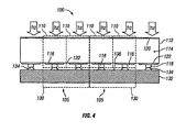
本発明はX線及びガンマ線輻射エネルギーを検出及び画像分析するための半導体装置の分野に関する。より詳細には、本発明は二つの異なる半導体基板上に多数の電気的に接近可能な点を持つピクセルセル内に電流を発生する装置上への入射輻射エネルギーにより画像分析が行なわれる、かかる装置に関する。特に、本発明は輻射線光子/パルスカウント像形成素子に関し、そこでは総体的に、ピクセルセルが光導電体/検出器基板上に加工された検出器ピクセルを持ち、この検出器ピクセルの数はカウント/読出し基板上に加工されたピクセルカウント回路の数より大きく、このピクセルカウント回路と検出器ピクセルは電気的に連通している。
1.各光子により発生される電荷パルスは個々に処理されるため、吸収された光子のエネルギーについての情報を提供することができる。このようにして光子はそれらのエネルギー水準に依存してカウントされまたは廃棄されることができる。低いエネルギーの光子は典型的にはもし廃棄されないと画像品質を低下させる四散光子であるため、これはまたコントラスト解像度を強化する。
2.光子パルスのため電子信号はデジタル化され、かつカウントされるので、この装置は背景雑音、検出器漏洩/暗電流等にそんなに敏感ではない。“暗電流”は衝突輻射線の存在を欠く装置内の背景電流であることに注意されたい。
3.外部デジタル化に対する必要はない。なぜならそれは“オンチップ”でなされ、それが像形成システムをより簡単にかつ潜在的に安価とする。
現在最も望ましくかつ最も輻射線吸収性のCdTe及びCdZnTeのような光導電体材料を利用する像形成素子において、エネルギー分解能は“ホールトラッピング”により制限される。簡単に言えば、高エネルギー光子がこれらの半導体検出器材料内に捕獲される毎に、等量の電子及びホール信号が発生される。電子は全く移動しやすく、検出器ピクセルの電子コレクタ電極に比較的早く到達する。しかし、ホールは電子に比べてかなりゆっくりと移動し、ホールがそれらの移動(例えば負に荷電した電極に向けての)を完了することができる前にそれらはトラップされる。結果として最終誘導信号はエネルギー分解能が損なわれる。
電子が電荷コレクタ検出器ピクセルに向けてドリフトするとき、それらはまた横方向に離れるようにドリフトする。光導電体検出器材料の厚さ及び吸収された光子のエネルギーに依存して、電荷パッケージが検出器ピクセルに到達する時間までに電荷パッケージの寸法が増え、その電荷密度は減少している。もし検出器ピクセルが項目(1)によりホールトラッピングに対する補償のためより小さくされたなら、そのときは電荷パッケージは一つより多いピクセルにより共有されるであろう。この検出器ピクセル間の電荷共有は電荷パッケージの共有を受けるピクセル検出器と組み合わされたピクセル信号カウント回路中に誤記号(ヒットまたはミス)を作りうる。なぜなら一つの当初から大きなパルスは二つの別個の小さなパルスとして見られるからである。
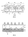
図1Aは従来技術のSBBASIC型半導体輻射線像形成素子の断面の概略側面図であり、そこでは各ピクセル回路は単一の検出器ピクセルと組み合わされており、また逆もまた同様であり、ピクセル検出器の数とピクセル回路の間の対応比1をもつ像形成素子を示す。
Claims (13)
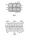
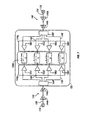
- 複数の連結検出器ピクセルセルを備え、
前記複数の連結検出器ピクセルセルの各々は、
半導体検出器基板上に配置された複数の検出器ピクセルを有する検出器ピクセルアレイと、
ASIC読出し基板上に配置された単一のピクセル信号カウント回路と
を有し、
前記ASIC読出し基板の一の面である読出し表面は、前記半導体検出器基板の一の面であるピクセル表面に対向して配置されており、
前記複数の検出器ピクセルの各々は、前記単一のピクセルセル信号カウント回路と電気的に連通している
ことを特徴とするX線及びガンマ線輻射エネルギー像形成素子。 - 前記複数の検出器ピクセルの各々は、
前記ピクセル表面上に配置され、前記半導体検出器基板内に発生した電荷を集めるためのコレクタ電極と、
前記コレクタ電極と前記単一のピクセル信号カウント回路との間に配置され、前記集められた電荷を前記単一のピクセル信号カウント回路へ伝導するピクセルコンタクトと
を有することを特徴とする請求項1に記載のX線及びガンマ線輻射エネルギー像形成素子。 - 前記単一のピクセル信号カウント回路は、前記単一のピクセル信号カウント回路と電気的に連通し、前記複数の検出器ピクセルに夫々対応する複数のピクセル信号入力部を有することを特徴とする請求項1に記載のX線及びガンマ線輻射エネルギー像形成素子。
- 前記複数の検出器ピクセルの各々は、前記半導体検出器基板内に発生した電荷を前記単一のピクセル信号カウント回路へ伝導するピクセルコンタクトを有し、
前記複数のピクセル信号入力部の各々は、対応するピクセルコンタクトに電気的に連通している
ことを特徴とする請求項3に記載のX線及びガンマ線輻射エネルギー像形成素子。 - 前記複数のピクセル信号入力部の各々は、ピクセル信号状態調節回路を含むことを特徴とする請求項4に記載のX線及びガンマ線輻射エネルギー像形成素子。
- 前記複数のピクセル信号入力部の各々は、信号増幅回路要素、暗電流補償回路要素、パルス幅制御回路要素、利得制御回路要素、パルス形状付与回路要素、比較回路要素、アナログ加算回路要素及び緩衝回路要素からなる群から選ばれた少なくとも一つの付随的状態調節/処理回路要素を含むピクセル信号状態調節回路を含むことを特徴とする請求項4に記載のX線及びガンマ線輻射エネルギー像形成素子。
- 前記ピクセルコンタクトは、緩衝結合であることを特徴とする請求項2に記載のX線及びガンマ線輻射エネルギー像形成素子。
- 前記ピクセルコンタクトは、ハンダ付け緩衝結合であることを特徴とする請求項2に記載のX線及びガンマ線輻射エネルギー像形成素子。
- 少なくとも一つの連結検出器ピクセルセルを備え、
前記連結検出器ピクセルセルは、
半導体検出器基板に配置された複数の検出器ピクセルを有する検出器ピクセルアレイと、
前記半導体検出器基板に対向して配置されたASIC読出し基板に配置され、前記複数の検出器ピクセルの少なくとも一部と電気的に連通されたピクセル信号カウント回路と
を有し、
前記ピクセル信号カウント回路の個数は、前記複数の検出器ピクセルの個数より少ない
ことを特徴とするX線及びガンマ線輻射エネルギー像形成素子。 - 前記検出器ピクセルアレイは、前記検出器ピクセルを少なくとも4つ有し、
前記少なくとも4つの検出器ピクセルの各々は、前記単一のピクセル信号カウント回路と電気的に連通している
ことを特徴とする請求項1に記載のX線及びガンマ線輻射エネルギー像形成素子。 - 前記複数の検出器ピクセルの各々は、前記ピクセル表面上に配置されたコレクタ電極を有し、
複数の前記コレクタ電極の平坦面積の合計としての前記検出器ピクセルアレイの平坦面積は、前記単一のピクセル信号カウント回路の平坦面積と少なくとも同じである
ことを特徴とする請求項1に記載のX線及びガンマ線輻射エネルギー像形成素子。 - 高エネルギー輻射線デジタル像形成素子で使用するための連結検出器ピクセルセルであって、
半導体検出器基板上に密接して配置された複数の検出器ピクセルを有する検出器ピクセルアレイと、
前記半導体検出器基板に対向して配置されたASIC読出し基板上に配置された単一のピクセル信号カウント回路と
を備え、
前記複数の検出器ピクセルの全ては、前記単一のピクセル信号カウント回路と電気的に連通している
ことを特徴とする連結検出器ピクセルセル。 - 前記単一のピクセル信号カウント回路の数に対する前記複数の検出器ピクセルの数の対応比が少なくとも2であることを特徴とする請求項12に記載の連結検出器ピクセルセル。
Applications Claiming Priority (3)
| Application Number | Priority Date | Filing Date | Title |
|---|---|---|---|
| US10/194,336 US7361881B2 (en) | 2002-03-13 | 2002-07-11 | Ganged detector pixel, photon/pulse counting radiation imaging device |
| US10/194,336 | 2002-07-11 | ||
| PCT/US2003/020839 WO2004008488A2 (en) | 2002-07-11 | 2003-07-03 | Ganged detector pixel, photon/pulse counting radiation imaging device |
Publications (2)
| Publication Number | Publication Date |
|---|---|
| JP2006506829A JP2006506829A (ja) | 2006-02-23 |
| JP4780765B2 true JP4780765B2 (ja) | 2011-09-28 |
Family
ID=30114714
Family Applications (1)
| Application Number | Title | Priority Date | Filing Date |
|---|---|---|---|
| JP2005512631A Expired - Fee Related JP4780765B2 (ja) | 2002-07-11 | 2003-07-03 | 連結検出器ピクセル、光子/パルスカウント輻射線像形成素子 |
Country Status (5)
| Country | Link |
|---|---|
| US (1) | US7361881B2 (ja) |
| EP (1) | EP1540730B1 (ja) |
| JP (1) | JP4780765B2 (ja) |
| ES (1) | ES2679099T3 (ja) |
| WO (1) | WO2004008488A2 (ja) |
Families Citing this family (26)
| Publication number | Priority date | Publication date | Assignee | Title |
|---|---|---|---|---|
| US7361881B2 (en) * | 2002-03-13 | 2008-04-22 | Oy Ajat Ltd | Ganged detector pixel, photon/pulse counting radiation imaging device |
| US7208739B1 (en) | 2005-11-30 | 2007-04-24 | General Electric Company | Method and apparatus for correction of pileup and charge sharing in x-ray images with energy resolution |
| US7633068B2 (en) * | 2006-03-15 | 2009-12-15 | Endicott Interconnect Technologies, Inc. | Count uniformity correction in flux space for pixilated semiconducting radiation detectors |
| US8354650B2 (en) * | 2006-03-22 | 2013-01-15 | Endicott Interconnect Technologies, Inc. | Multi-window signal processing electronics architecture for photon counting with multi-element sensors |
| US7682930B2 (en) * | 2006-06-09 | 2010-03-23 | Aptina Imaging Corporation | Method of forming elevated photosensor and resulting structure |
| EP2054738A2 (en) * | 2006-08-14 | 2009-05-06 | Koninklijke Philips Electronics N.V. | Radiation detector with counting electronics |
| GB2444777B (en) * | 2006-12-13 | 2011-06-29 | Lancaster University | Detection of radiation |
| EP2225589B1 (en) * | 2007-12-20 | 2014-07-16 | Koninklijke Philips N.V. | Direct conversion detector |
| GB2466213B (en) * | 2008-12-12 | 2013-03-06 | Cmosis Nv | Pixel array with shared readout circuitry |
| CA2755076C (en) | 2009-04-29 | 2016-07-05 | Xcounter Ab | Computed tomography scanning system |
| FI122647B (fi) * | 2009-06-09 | 2012-05-15 | Planmeca Oy | Digitaaliröntgenanturijärjestely ja digitaalinen röntgenkuvantamismenetelmä |
| JP5521721B2 (ja) | 2009-08-28 | 2014-06-18 | ソニー株式会社 | 撮像素子およびカメラシステム |
| TWI559763B (zh) * | 2009-10-01 | 2016-11-21 | 索尼半導體解決方案公司 | 影像取得裝置及照相機系統 |
| KR101634250B1 (ko) * | 2010-06-21 | 2016-06-28 | 삼성전자주식회사 | 대면적 엑스선 검출기 및 제조방법 |
| EP2407109B1 (en) | 2010-07-14 | 2016-01-06 | XCounter AB | Computed tomography scanning system and method |
| US9310495B2 (en) | 2011-05-04 | 2016-04-12 | Oy Ajat Ltd. | Photon/energy identifying X-ray and gamma ray imaging device (“PID”) with a two dimensional array of pixels and system therefrom |
| DE102011077859B4 (de) | 2011-06-21 | 2014-01-23 | Siemens Aktiengesellschaft | Quantenzählender Strahlungsdetektor |
| US9036065B1 (en) | 2012-08-16 | 2015-05-19 | Rambus Inc. | Shared-counter image sensor |
| US9261609B2 (en) | 2012-08-20 | 2016-02-16 | General Electric Company | Apparatus and methods for charge collection control in radiation detectors |
| JP6790058B2 (ja) | 2015-07-13 | 2020-11-25 | コーニンクレッカ フィリップス エヌ ヴェKoninklijke Philips N.V. | 高エネルギー分解能/高x線フラックス光子計数検出器 |
| EP3347741B1 (en) * | 2015-09-08 | 2020-05-20 | Shenzhen Xpectvision Technology Co., Ltd. | Methods for making an x-ray detector |
| US10117626B2 (en) * | 2015-09-29 | 2018-11-06 | General Electric Company | Apparatus and method for pile-up correction in photon-counting detector |
| US10375168B2 (en) * | 2016-05-31 | 2019-08-06 | Veritas Technologies Llc | Throughput in openfabrics environments |
| JP6877772B2 (ja) * | 2016-10-27 | 2021-05-26 | 株式会社リガク | 検出器 |
| JP7179177B2 (ja) * | 2018-11-19 | 2022-11-28 | プリズマティック、センサーズ、アクチボラグ | エッジオン光子計数検出器 |
| CA3191565A1 (en) * | 2020-09-02 | 2022-03-10 | The Research Foundation For The State University Of New York | Tapered scintillator crystal modules and methods of using the same |
Family Cites Families (37)
| Publication number | Priority date | Publication date | Assignee | Title |
|---|---|---|---|---|
| US5146406A (en) * | 1989-08-16 | 1992-09-08 | International Business Machines Corporation | Computer method for identifying predicate-argument structures in natural language text |
| US5262871A (en) * | 1989-11-13 | 1993-11-16 | Rutgers, The State University | Multiple resolution image sensor |
| JP2890553B2 (ja) * | 1989-11-24 | 1999-05-17 | 株式会社島津製作所 | X線像撮像装置 |
| EP0494573A1 (en) * | 1991-01-08 | 1992-07-15 | International Business Machines Corporation | Method for automatically disambiguating the synonymic links in a dictionary for a natural language processing system |
| US5377103A (en) * | 1992-05-15 | 1994-12-27 | International Business Machines Corporation | Constrained natural language interface for a computer that employs a browse function |
| US5369575A (en) * | 1992-05-15 | 1994-11-29 | International Business Machines Corporation | Constrained natural language interface for a computer system |
| US5630121A (en) * | 1993-02-02 | 1997-05-13 | International Business Machines Corporation | Archiving and retrieving multimedia objects using structured indexes |
| GB2279164A (en) * | 1993-06-18 | 1994-12-21 | Canon Res Ct Europe Ltd | Processing a bilingual database. |
| JP3408291B2 (ja) * | 1993-09-20 | 2003-05-19 | 株式会社東芝 | 辞書作成支援装置 |
| US5659765A (en) * | 1994-03-15 | 1997-08-19 | Toppan Printing Co., Ltd. | Machine translation system |
| GB2289983B (en) * | 1994-06-01 | 1996-10-16 | Simage Oy | Imaging devices,systems and methods |
| US5799268A (en) * | 1994-09-28 | 1998-08-25 | Apple Computer, Inc. | Method for extracting knowledge from online documentation and creating a glossary, index, help database or the like |
| US5665959A (en) * | 1995-01-13 | 1997-09-09 | The United States Of America As Represented By The Administrator Of The National Aeronautics And Space Adminstration | Solid-state image sensor with focal-plane digital photon-counting pixel array |
| DE19503364C2 (de) * | 1995-02-02 | 1999-08-26 | Siemens Ag | Röntgenbildaufnahmesystem |
| GB2318411B (en) * | 1996-10-15 | 1999-03-10 | Simage Oy | Imaging device for imaging radiation |
| US6085162A (en) * | 1996-10-18 | 2000-07-04 | Gedanken Corporation | Translation system and method in which words are translated by a specialized dictionary and then a general dictionary |
| US6011531A (en) * | 1996-10-21 | 2000-01-04 | Xerox Corporation | Methods and applications of combining pixels to the gate and data lines for 2-D imaging and display arrays |
| GB2319394B (en) * | 1996-12-27 | 1998-10-28 | Simage Oy | Bump-bonded semiconductor imaging device |
| US6207944B1 (en) * | 1997-02-18 | 2001-03-27 | Simage, O.Y. | Semiconductor imaging device |
| US5991710A (en) * | 1997-05-20 | 1999-11-23 | International Business Machines Corporation | Statistical translation system with features based on phrases or groups of words |
| US6078878A (en) * | 1997-07-31 | 2000-06-20 | Microsoft Corporation | Bootstrapping sense characterizations of occurrences of polysemous words |
| US6107655A (en) * | 1997-08-15 | 2000-08-22 | Eastman Kodak Company | Active pixel image sensor with shared amplifier read-out |
| US6069362A (en) * | 1998-05-14 | 2000-05-30 | The University Of Akron | Multi-density and multi-atomic number detector media for applications |
| JP3114703B2 (ja) * | 1998-07-02 | 2000-12-04 | 富士ゼロックス株式会社 | 対訳文検索装置 |
| US6285978B1 (en) * | 1998-09-24 | 2001-09-04 | International Business Machines Corporation | System and method for estimating accuracy of an automatic natural language translation |
| US6175611B1 (en) * | 1998-10-06 | 2001-01-16 | Cardiac Mariners, Inc. | Tiered detector assembly |
| US6181775B1 (en) * | 1998-11-25 | 2001-01-30 | Westell Technologies, Inc. | Dual test mode network interface unit for remote testing of transmission line and customer equipment |
| AU4603200A (en) * | 1999-04-26 | 2000-11-10 | Simage Oy | Device for imaging radiation |
| DE19938793A1 (de) * | 1999-08-16 | 2001-04-12 | Siemens Ag | CT-Gerät mit mehrzeiligem Detekorsystem |
| US6393389B1 (en) * | 1999-09-23 | 2002-05-21 | Xerox Corporation | Using ranked translation choices to obtain sequences indicating meaning of multi-token expressions |
| US6330530B1 (en) * | 1999-10-18 | 2001-12-11 | Sony Corporation | Method and system for transforming a source language linguistic structure into a target language linguistic structure based on example linguistic feature structures |
| EP1102323B1 (en) * | 1999-11-19 | 2012-08-15 | CSEM Centre Suisse d'Electronique et de Microtechnique SA - Recherche et Développement | Method for detecting electromagnetic radiation using an optoelectronic sensor |
| US7962326B2 (en) * | 2000-04-20 | 2011-06-14 | Invention Machine Corporation | Semantic answering system and method |
| AU2002221005A1 (en) * | 2000-11-27 | 2002-06-03 | Vision Sciences, Inc. | Programmable resolution cmos image sensor |
| US7189971B2 (en) * | 2002-02-15 | 2007-03-13 | Oy Ajat Ltd | Radiation imaging device and system |
| US6933505B2 (en) * | 2002-03-13 | 2005-08-23 | Oy Ajat Ltd | Low temperature, bump-bonded radiation imaging device |
| US7361881B2 (en) * | 2002-03-13 | 2008-04-22 | Oy Ajat Ltd | Ganged detector pixel, photon/pulse counting radiation imaging device |
-
2002
- 2002-07-11 US US10/194,336 patent/US7361881B2/en not_active Expired - Fee Related
-
2003
- 2003-07-03 EP EP03817490.0A patent/EP1540730B1/en not_active Expired - Lifetime
- 2003-07-03 ES ES03817490.0T patent/ES2679099T3/es not_active Expired - Lifetime
- 2003-07-03 WO PCT/US2003/020839 patent/WO2004008488A2/en active Search and Examination
- 2003-07-03 JP JP2005512631A patent/JP4780765B2/ja not_active Expired - Fee Related
Also Published As
| Publication number | Publication date |
|---|---|
| WO2004008488A8 (en) | 2005-02-17 |
| EP1540730A4 (en) | 2007-07-11 |
| US7361881B2 (en) | 2008-04-22 |
| WO2004008488A3 (en) | 2004-09-02 |
| US20030173522A1 (en) | 2003-09-18 |
| WO2004008488A2 (en) | 2004-01-22 |
| EP1540730B1 (en) | 2018-06-13 |
| WO2004008488A9 (en) | 2004-06-10 |
| ES2679099T3 (es) | 2018-08-22 |
| JP2006506829A (ja) | 2006-02-23 |
| EP1540730A2 (en) | 2005-06-15 |
Similar Documents
| Publication | Publication Date | Title |
|---|---|---|
| JP4780765B2 (ja) | 連結検出器ピクセル、光子/パルスカウント輻射線像形成素子 | |
| US6002134A (en) | Cross-strip semiconductor detector with cord-wood construction | |
| US5693947A (en) | Radiation detectors | |
| EP0722188B1 (en) | Image capture panel using a solid state device | |
| JP4989005B2 (ja) | デジタルx線撮像の方法及びセンサ装置 | |
| US7064338B2 (en) | Two-dimensional radiation detector | |
| US5099128A (en) | High resolution position sensitive detector | |
| US6037595A (en) | Radiation detector with shielding electrode | |
| EP0239808B1 (en) | Radiation detecting device | |
| US5220170A (en) | X-ray imaging system and solid state detector therefor | |
| EP2005215B1 (en) | Multi-layer pixellated gamma-ray detector | |
| US5929449A (en) | Flat panel detector for radiation imaging with reduced electronic noise | |
| JPH11515093A (ja) | 捕捉電荷が減少する放射線イメージング用フラットパネル検出器 | |
| US7233003B2 (en) | Radiation detector | |
| US20050184244A1 (en) | Radiation detector and light or radiation detector | |
| US20010035497A1 (en) | Detector support device for detecting ionizing radiations | |
| JPH0784055A (ja) | 放射線2次元検出器 | |
| US6080997A (en) | Electromagnetic-wave detector | |
| US6373062B1 (en) | Interdigital photodetector for indirect x-ray detection in a radiography imaging system | |
| US20110291020A1 (en) | Edge-on two-dimensional detector arrays | |
| US20160161426A1 (en) | Pillar Based Amorphous and Polycrystalline Photoconductors for X-ray Image Sensors | |
| US6586742B2 (en) | Method and arrangement relating to x-ray imaging | |
| JP2000046951A (ja) | 放射線検出素子 | |
| JPH07107942B2 (ja) | 放射線検出装置 | |
| JPS6386472A (ja) | 固体撮像素子 |
Legal Events
| Date | Code | Title | Description |
|---|---|---|---|
| A621 | Written request for application examination |
Free format text: JAPANESE INTERMEDIATE CODE: A621 Effective date: 20060605 |
|
| A977 | Report on retrieval |
Free format text: JAPANESE INTERMEDIATE CODE: A971007 Effective date: 20091007 |
|
| A131 | Notification of reasons for refusal |
Free format text: JAPANESE INTERMEDIATE CODE: A131 Effective date: 20091016 |
|
| A601 | Written request for extension of time |
Free format text: JAPANESE INTERMEDIATE CODE: A601 Effective date: 20091211 |
|
| A602 | Written permission of extension of time |
Free format text: JAPANESE INTERMEDIATE CODE: A602 Effective date: 20091218 |
|
| A521 | Request for written amendment filed |
Free format text: JAPANESE INTERMEDIATE CODE: A821 Effective date: 20100325 |
|
| RD02 | Notification of acceptance of power of attorney |
Free format text: JAPANESE INTERMEDIATE CODE: A7422 Effective date: 20100325 |
|
| A521 | Request for written amendment filed |
Free format text: JAPANESE INTERMEDIATE CODE: A523 Effective date: 20100401 |
|
| RD04 | Notification of resignation of power of attorney |
Free format text: JAPANESE INTERMEDIATE CODE: A7424 Effective date: 20100407 |
|
| A521 | Request for written amendment filed |
Free format text: JAPANESE INTERMEDIATE CODE: A821 Effective date: 20100325 |
|
| TRDD | Decision of grant or rejection written | ||
| A01 | Written decision to grant a patent or to grant a registration (utility model) |
Free format text: JAPANESE INTERMEDIATE CODE: A01 Effective date: 20110621 |
|
| A01 | Written decision to grant a patent or to grant a registration (utility model) |
Free format text: JAPANESE INTERMEDIATE CODE: A01 |
|
| A61 | First payment of annual fees (during grant procedure) |
Free format text: JAPANESE INTERMEDIATE CODE: A61 Effective date: 20110704 |
|
| FPAY | Renewal fee payment (event date is renewal date of database) |
Free format text: PAYMENT UNTIL: 20140715 Year of fee payment: 3 |
|
| R150 | Certificate of patent or registration of utility model |
Ref document number: 4780765 Country of ref document: JP Free format text: JAPANESE INTERMEDIATE CODE: R150 Free format text: JAPANESE INTERMEDIATE CODE: R150 |
|
| R250 | Receipt of annual fees |
Free format text: JAPANESE INTERMEDIATE CODE: R250 |
|
| R250 | Receipt of annual fees |
Free format text: JAPANESE INTERMEDIATE CODE: R250 |
|
| R250 | Receipt of annual fees |
Free format text: JAPANESE INTERMEDIATE CODE: R250 |
|
| R250 | Receipt of annual fees |
Free format text: JAPANESE INTERMEDIATE CODE: R250 |
|
| R250 | Receipt of annual fees |
Free format text: JAPANESE INTERMEDIATE CODE: R250 |
|
| R250 | Receipt of annual fees |
Free format text: JAPANESE INTERMEDIATE CODE: R250 |
|
| R250 | Receipt of annual fees |
Free format text: JAPANESE INTERMEDIATE CODE: R250 |
|
| R250 | Receipt of annual fees |
Free format text: JAPANESE INTERMEDIATE CODE: R250 |
|
| LAPS | Cancellation because of no payment of annual fees |