JP4779110B2 - 二酸化クロム系ハーフメタル膜 - Google Patents
二酸化クロム系ハーフメタル膜 Download PDFInfo
- Publication number
- JP4779110B2 JP4779110B2 JP2005002768A JP2005002768A JP4779110B2 JP 4779110 B2 JP4779110 B2 JP 4779110B2 JP 2005002768 A JP2005002768 A JP 2005002768A JP 2005002768 A JP2005002768 A JP 2005002768A JP 4779110 B2 JP4779110 B2 JP 4779110B2
- Authority
- JP
- Japan
- Prior art keywords
- chromium dioxide
- film
- metal film
- metal
- chromium
- Prior art date
- Legal status (The legal status is an assumption and is not a legal conclusion. Google has not performed a legal analysis and makes no representation as to the accuracy of the status listed.)
- Expired - Lifetime
Links
Images
Landscapes
- Physical Vapour Deposition (AREA)
- Thin Magnetic Films (AREA)
- Hall/Mr Elements (AREA)
- Physical Deposition Of Substances That Are Components Of Semiconductor Devices (AREA)
Description
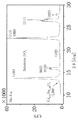
Cr83at%、Sn17at%の仕込み量でZrO2基板上に真空蒸着して作製した膜のX線回折パターンを図1に示す。基板ZrO2によるピークの他にCr0.81Sn0.19O2(110)面に相当するピークが観測され、添加元素Snが混入し、ルチル構造を形成していることを示す。
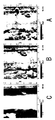
Bは、表面形状と同じ場所の磁場がかけられていないときの磁気力顕微鏡画像である。
Cは、表面形状像である。
Claims (2)
- 酸化物が二酸化クロムの結晶構造と同じルチル構造を有する元素としてのルテニウムを含有するとともに、ハーフメタル特性を有することを特徴とする二酸化クロム系ハーフメタル膜。
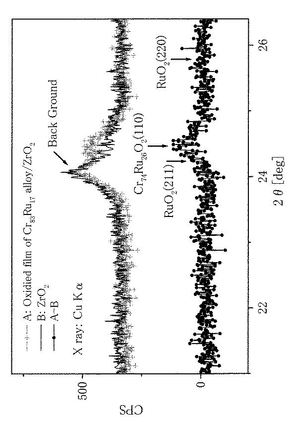
- 請求項1記載の二酸化クロム系ハーフメタル膜において、X線解析によりCr 74 Ru 26 O 2 の(110)のピークが示されることを特徴とする二酸化クロム系ハーフメタル膜。
Priority Applications (1)
| Application Number | Priority Date | Filing Date | Title |
|---|---|---|---|
| JP2005002768A JP4779110B2 (ja) | 2005-01-07 | 2005-01-07 | 二酸化クロム系ハーフメタル膜 |
Applications Claiming Priority (1)
| Application Number | Priority Date | Filing Date | Title |
|---|---|---|---|
| JP2005002768A JP4779110B2 (ja) | 2005-01-07 | 2005-01-07 | 二酸化クロム系ハーフメタル膜 |
Publications (2)
| Publication Number | Publication Date |
|---|---|
| JP2006188740A JP2006188740A (ja) | 2006-07-20 |
| JP4779110B2 true JP4779110B2 (ja) | 2011-09-28 |
Family
ID=36796201
Family Applications (1)
| Application Number | Title | Priority Date | Filing Date |
|---|---|---|---|
| JP2005002768A Expired - Lifetime JP4779110B2 (ja) | 2005-01-07 | 2005-01-07 | 二酸化クロム系ハーフメタル膜 |
Country Status (1)
| Country | Link |
|---|---|
| JP (1) | JP4779110B2 (ja) |
Family Cites Families (3)
| Publication number | Priority date | Publication date | Assignee | Title |
|---|---|---|---|---|
| JPH1197766A (ja) * | 1997-09-17 | 1999-04-09 | Res Inst Electric Magnetic Alloys | 強磁性トンネル接合素子 |
| JP2000150899A (ja) * | 1998-11-17 | 2000-05-30 | Hitachi Ltd | 薄膜形成方法 |
| JP3550524B2 (ja) * | 2000-03-10 | 2004-08-04 | シャープ株式会社 | 磁気抵抗効果素子及びそれを用いた磁気メモリ |
-
2005
- 2005-01-07 JP JP2005002768A patent/JP4779110B2/ja not_active Expired - Lifetime
Also Published As
| Publication number | Publication date |
|---|---|
| JP2006188740A (ja) | 2006-07-20 |
Similar Documents
| Publication | Publication Date | Title |
|---|---|---|
| Mittmann et al. | Origin of ferroelectric phase in undoped HfO2 films deposited by sputtering | |
| CN102687297B (zh) | 磁阻元件的制造方法 | |
| JP6857421B2 (ja) | 強磁性トンネル接合体、それを用いたスピントロニクスデバイス、及び強磁性トンネル接合体の製造方法 | |
| JP6690838B2 (ja) | 強磁性トンネル接合体、これを用いた磁気抵抗効果素子及びスピントロニクスデバイス並びに強磁性トンネル接合体の製造方法 | |
| JP4945704B2 (ja) | 磁気トンネル接合素子 | |
| TW200421358A (en) | Small and high performance, rare earth permanent magnet for micro applications and method for preparation thereof | |
| EP3933948A1 (en) | Magnetoresistive stack, seed region therefor and method of manufacturing same | |
| JP6713650B2 (ja) | 垂直磁化膜と垂直磁化膜構造並びに磁気抵抗素子および垂直磁気記録媒体 | |
| US20200043979A1 (en) | Magnetoresistive stack with seed region and method of manufacturing the same | |
| Kim et al. | Top Electrode Engineering for High‐Performance Ferroelectric Hf0. 5Zr0. 5O2 Capacitors | |
| JP6873506B2 (ja) | 垂直磁化膜の前駆体構造、垂直磁化膜構造、およびその製造方法、これらを用いた垂直磁化型トンネル磁気抵抗接合膜およびその製造方法、ならびにこれらを用いた垂直磁化型トンネル磁気抵抗接合素子 | |
| KR20190046653A (ko) | 반도체 장치 | |
| JP4779110B2 (ja) | 二酸化クロム系ハーフメタル膜 | |
| CN1165777C (zh) | 磁检测器及其制造方法,以及使用它的磁头 | |
| JP6583814B2 (ja) | 垂直磁化膜構造およびその製造方法、それを用いた磁気抵抗素子およびその製造方法、ならびにこれらを用いたスピントロニクスデバイス | |
| Li et al. | Effects of Nb doping on switching-voltage stability of zinc oxide thin films | |
| JP2017098538A (ja) | Mn−X系磁性材料 | |
| WO2001056090A1 (en) | Magnetoresistance effect device and method for manufacturing the same, base for magnetoresistance effect device and method for manufacturing the same, and magnetoresistance effect sensor | |
| JPH06140687A (ja) | 磁気抵抗素子用磁性薄膜およびその製造方法 | |
| JP4953064B2 (ja) | ホイスラー合金とそれを用いたtmr素子又はgmr素子 | |
| Hu et al. | Resistive switching characteristics of manganese oxide nanoparticle assembly with crossbar arrays | |
| JP2009212480A (ja) | 強磁性薄膜材料とその製造方法 | |
| Iwata et al. | Microscopic Investigation of the Electrical and Structural Properties of Conductive Filaments Formed in Pt/NiO/Pt Resistive Switching Cells | |
| JP3602013B2 (ja) | 強磁性トンネル接合素子の製造方法 | |
| Niizeki et al. | Nanofabrication of magnetic tunnel junctions by using side-edge thin film deposition |
Legal Events
| Date | Code | Title | Description |
|---|---|---|---|
| A621 | Written request for application examination |
Free format text: JAPANESE INTERMEDIATE CODE: A621 Effective date: 20071015 |
|
| A977 | Report on retrieval |
Free format text: JAPANESE INTERMEDIATE CODE: A971007 Effective date: 20091218 |
|
| A131 | Notification of reasons for refusal |
Free format text: JAPANESE INTERMEDIATE CODE: A131 Effective date: 20101214 |
|
| A521 | Request for written amendment filed |
Free format text: JAPANESE INTERMEDIATE CODE: A523 Effective date: 20110214 |
|
| RD02 | Notification of acceptance of power of attorney |
Free format text: JAPANESE INTERMEDIATE CODE: A7422 Effective date: 20110214 |
|
| A521 | Request for written amendment filed |
Free format text: JAPANESE INTERMEDIATE CODE: A523 Effective date: 20110401 |
|
| A521 | Request for written amendment filed |
Free format text: JAPANESE INTERMEDIATE CODE: A821 Effective date: 20110401 |
|
| TRDD | Decision of grant or rejection written | ||
| A01 | Written decision to grant a patent or to grant a registration (utility model) |
Free format text: JAPANESE INTERMEDIATE CODE: A01 Effective date: 20110607 |
|
| A01 | Written decision to grant a patent or to grant a registration (utility model) |
Free format text: JAPANESE INTERMEDIATE CODE: A01 |
|
| A61 | First payment of annual fees (during grant procedure) |
Free format text: JAPANESE INTERMEDIATE CODE: A61 Effective date: 20110623 |
|
| R150 | Certificate of patent or registration of utility model |
Ref document number: 4779110 Country of ref document: JP Free format text: JAPANESE INTERMEDIATE CODE: R150 Free format text: JAPANESE INTERMEDIATE CODE: R150 |
|
| EXPY | Cancellation because of completion of term |