JP4779110B2 - Chromium dioxide half metal film - Google Patents
Chromium dioxide half metal film Download PDFInfo
- Publication number
- JP4779110B2 JP4779110B2 JP2005002768A JP2005002768A JP4779110B2 JP 4779110 B2 JP4779110 B2 JP 4779110B2 JP 2005002768 A JP2005002768 A JP 2005002768A JP 2005002768 A JP2005002768 A JP 2005002768A JP 4779110 B2 JP4779110 B2 JP 4779110B2
- Authority
- JP
- Japan
- Prior art keywords
- chromium dioxide
- film
- metal film
- metal
- chromium
- Prior art date
- Legal status (The legal status is an assumption and is not a legal conclusion. Google has not performed a legal analysis and makes no representation as to the accuracy of the status listed.)
- Expired - Lifetime
Links
Images
Landscapes
- Physical Vapour Deposition (AREA)
- Thin Magnetic Films (AREA)
- Hall/Mr Elements (AREA)
- Physical Deposition Of Substances That Are Components Of Semiconductor Devices (AREA)
Description
本発明は、ハーフメタル特性を有する材料に関し、特に、安価で製造が容易な、二酸化クロム系ハーフメタル膜に関する。 The present invention relates to a material having half-metal characteristics, and particularly to a chromium dioxide-based half-metal film that is inexpensive and easy to manufacture.
磁性酸化物ハーフメタル材料として、二酸化クロムが知られている(非特許文献1を参照)。渡辺らは、温度上昇で強磁性の性質が消失し、また降温で強磁性が出現する温度、すなわちキュリー点が室温以上を有するハーフメタル材料としてマグネタイトと二酸化クロムを上げている(特許文献1)。ハーフメタル材料とは、アップスピンとダウンスピンというスピンの向きがまったく異なる2種類の電子のうち、一方が金属的に振る舞い、一方が絶縁体的あるいは半導体的に振る舞うため、100%一方だけの向きを持つスピン偏極した伝導電子を有する材料を言う。強磁性は磁化測定、磁気力顕微鏡画像の磁場変化などにより明らかにすることが出来、強磁性転移温度のキュリー点は磁化の温度変化、電気抵抗の温度変化の傾き変化などから決めることができる。
二酸化クロムのキュリー点は約120℃であるために、室温ではハーフメタル特性が小さくなり、室温付近での電子素子用材料としては適さないという問題があり、室温で優れた特性が生じるために、キュリー温度を高くする必要があった。又、従来の成膜技術では化学気相成長法で膜を作製するため、所望の形の膜パターンを形成させるために高価な装置を用いる方法をとる必要があり価格が高くなり、又、ガスが回り込み、必要な箇所に適切に膜を作るのが困難という問題も抱えていた。そのため、安価にしかも所望の箇所に成膜する方法を必要としていた。 Since the Curie point of chromium dioxide is about 120 ° C., the half-metal characteristics become small at room temperature, and there is a problem that it is not suitable as an electronic device material near room temperature. It was necessary to raise the Curie temperature. In addition, in the conventional film formation technique, a film is formed by a chemical vapor deposition method, so that it is necessary to use a method using an expensive apparatus to form a film pattern of a desired shape. However, there was a problem that it was difficult to properly form a film at a necessary place. Therefore, a method for forming a film at a desired location at a low cost is required.
本発明の二酸化クロム系ハーフメタル膜は、酸化物が二酸化クロムの結晶構造と同じルチル構造を有する元素としてのルテニウムを含有するとともに、ハーフメタル特性を有することを特徴とする。本発明の二酸化クロム系ハーフメタル膜において、X線解析によりCr 74 Ru 26 O 2 の(110)のピークが示されることが好ましい。二酸化クロムにクロム以外の元素を一部含有させ、二酸化クロムと同じルチル結晶構造を取ることによって、二酸化クロム単独よりも高いキュリー温度を達成できることを実験的に本発明者らは見いだした。最近、我々が行った分子軌道法による理論計算においても、ルテニウム、錫、モリブデン、タングステンなどを添加元素とした二酸化クロムにおいて、ハーフメタルの性質を有しながらキュリー温度が上昇する結果を得ている。また、一般的な蒸着法を適用させ、マスクを使い所望の形にして膜を形成することができ、したがって安価にしかも容易に膜を作製する方法を提供するものである。又、高速の希ガス・イオンを発生させ、蒸発源の元素あるいは分子を弾き飛ばして蒸着させるスパッタリング法や、レーザーを使い元素あるいは分子を蒸発させて蒸着させるレーザーアブレーション法などを適用させてもよい。 The chromium dioxide half metal film of the present invention is characterized in that the oxide contains ruthenium as an element having the same rutile structure as the crystal structure of chromium dioxide and has half metal characteristics. In the chromium dioxide half metal film of the present invention, it is preferable that the (110) peak of Cr 74 Ru 26 O 2 is shown by X-ray analysis . The inventors have experimentally found that a higher Curie temperature than that of chromium dioxide alone can be achieved by incorporating some elements other than chromium into chromium dioxide and adopting the same rutile crystal structure as chromium dioxide. Recently, the theoretical calculation by the molecular orbital method we performed also showed that the Curie temperature rises while having the properties of a half metal in chromium dioxide containing ruthenium, tin, molybdenum, tungsten, etc. as additive elements. . Further , it is possible to form a film in a desired shape using a mask by applying a general vapor deposition method, and thus provide a method for easily and inexpensively forming a film. In addition, a sputtering method in which high-speed rare gas ions are generated and elements or molecules of the evaporation source are blown off to be deposited or a laser ablation method in which elements or molecules are evaporated by using a laser may be applied. .
得られた強磁性膜のキュリー温度が上昇し、室温付近での電子素子用の材料として使用可能となり、一般的な蒸着法で簡単に成膜できるので、簡単に比較的安価に膜を提供することが可能となる。 Since the Curie temperature of the obtained ferromagnetic film rises, it can be used as a material for an electronic device near room temperature, and can be easily formed by a general vapor deposition method. Therefore, the film can be easily provided at a relatively low cost. It becomes possible.
二酸化クロムに含有させる元素としては、酸化物が二酸化クロムの結晶構造と同じルチル構造を与える元素を使うことができる。その中でも、ルテニウム、錫、モリブデン、タングステンが好ましい。さらに、その含有させる元素は単独でも複数元素でもよい。膜の作製はクロムと添加元素の合金を作製後、真空蒸着法あるいはスパッタリング法やレーザーアブレーション法などにて成膜し、引き続き酸化処理する方法やクロムと添加元素を共蒸着法にて成膜し、その後に酸化処理して酸化物膜を得る方法、また、二酸化クロムとルチル構造を有する二酸化元素の共蒸着法にて作製することができる。 As an element to be contained in chromium dioxide, an element in which an oxide gives the same rutile structure as the crystal structure of chromium dioxide can be used. Among these, ruthenium, tin, molybdenum, and tungsten are preferable. Further, the element to be contained may be a single element or a plurality of elements. The film is made by forming an alloy of chromium and an additive element, and then depositing it by vacuum deposition, sputtering, laser ablation, etc., followed by oxidation or by co-evaporation of chromium and an additive element. Thereafter, it can be produced by a method of obtaining an oxide film by oxidation treatment, or a co-evaporation method of chromium dioxide and a dioxide element having a rutile structure.
アルゴン雰囲気中で気体放電させて合金をつくる、いわゆるアーク溶解法で合金化し、最終到達真空度1×10⁻⁴Paのチャンバー内で基板温度を室温にして膜厚約30nm蒸着し、その以後、膜を5時間酸化処理した。その他の作製法の条件を表1に列記する。
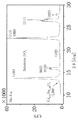
Cr83at%、Sn17at%の仕込み量でZrO2基板上に真空蒸着して作製した膜のX線回折パターンを図1に示す。基板ZrO2によるピークの他にCr0.81Sn0.19O2(110)面に相当するピークが観測され、添加元素Snが混入し、ルチル構造を形成していることを示す。
An alloy is produced by gas discharge in an argon atmosphere, alloyed by a so-called arc melting method, and deposited at a substrate temperature of room temperature in a chamber having a final ultimate vacuum of 1 × 10 −4 Pa. The membrane was oxidized for 5 hours. The conditions of other production methods are listed in Table 1.
FIG. 1 shows an X-ray diffraction pattern of a film prepared by vacuum deposition on a ZrO 2 substrate with a charge amount of Cr 83 at% and Sn 17 at%. In addition to the peak due to the substrate ZrO 2, a peak corresponding to the Cr 0.81 Sn 0.19 O 2 (110) plane is observed, indicating that the additive element Sn is mixed and a rutile structure is formed.
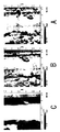
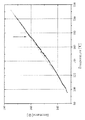
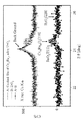
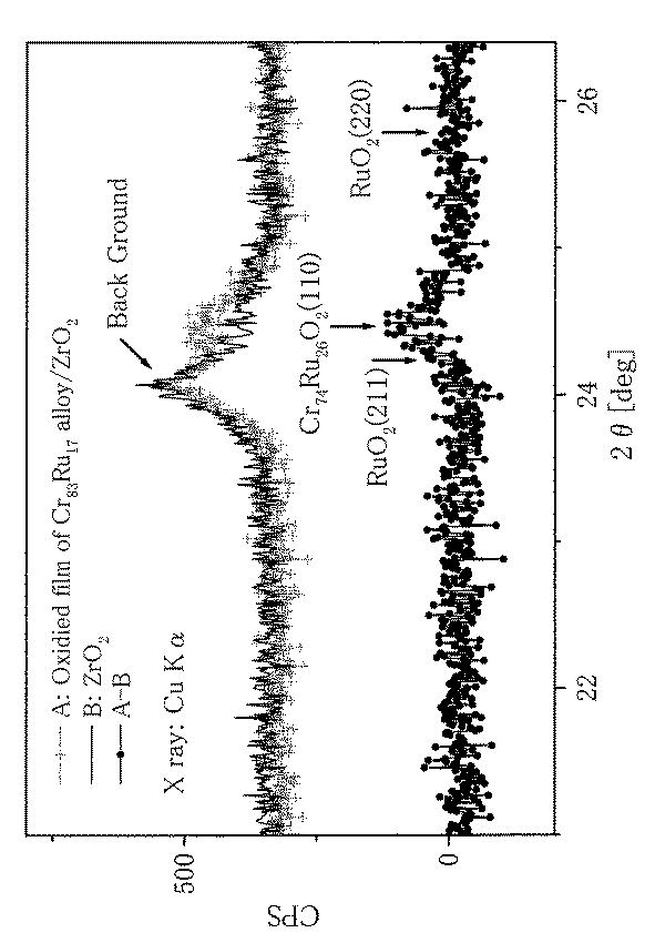
実施例1と同様に、Cr83at%、Ru17at%の仕込み料でZrO2基板上に真空蒸着して作製した膜における磁気力顕微鏡画像を、二酸化クロムのキュリー温度である約120℃より高い135℃で測定した。その結果を図2に示す。図は磁区が存在し、磁界により磁区が変化したことを示しており135℃でも強磁性が保持されていることを示している。また、図3に示すように、同じ試料における電気抵抗の温度変化の傾き変化から約180℃付近にキュリー温度を持つことが分かる。図4は膜のX線回折の測定結果を示す。図から分かるように仕込み量に近い組成のCr74Ru26O2における(110)のピークが見られ、Ruの元素が含まれたCrO2膜の存在を示している。又、走査型電子顕微鏡を用いた膜の元素組成分析においても、仕込み量に近い組成を示唆する結果が得られている。 As in Example 1, a magnetic force microscope image of a film prepared by vacuum deposition on a ZrO 2 substrate with a charge of Cr 83 at% and Ru 17 at% was obtained at 135 ° C., which is higher than about 120 ° C., which is the Curie temperature of chromium dioxide. It was measured. The result is shown in FIG. The figure shows that a magnetic domain exists and the magnetic domain is changed by a magnetic field, and that ferromagnetism is maintained even at 135 ° C. Moreover, as shown in FIG. 3, it turns out that it has a Curie temperature in about 180 degreeC from the inclination change of the temperature change of the electrical resistance in the same sample. FIG. 4 shows the measurement results of the X-ray diffraction of the film. As can be seen from the figure, a peak of (110) is observed in Cr 74 Ru 26 O 2 having a composition close to the charged amount, indicating the presence of a CrO 2 film containing the Ru element. Further, in the elemental composition analysis of the film using a scanning electron microscope, a result suggesting a composition close to the charged amount is obtained.
実施例1と同様に、蒸着の条件のみを表1中の実施例3に示す条件に変え実施し、実施例1、2と同様の結果が得られた。表1中の実施例4、5,6も同様の結果が得られた。 As in Example 1, only the deposition conditions were changed to the conditions shown in Example 3 in Table 1, and the same results as in Examples 1 and 2 were obtained. Similar results were obtained in Examples 4, 5 and 6 in Table 1.
本発明の膜はトンネル磁気抵抗効果を有する素子として、超高速磁気読み取りヘッドの構成部品として、あるいは磁気ランダムアクセスメモリー材料として利用される可能性を有している。 The film of the present invention has the potential to be used as an element having a tunnel magnetoresistive effect, as a component of an ultrafast magnetic read head, or as a magnetic random access memory material.
Aは、0.2Tの磁場が膜面の方向にかけられたときの磁気力顕微鏡画像である。
Bは、表面形状と同じ場所の磁場がかけられていないときの磁気力顕微鏡画像である。
Cは、表面形状像である。
A is a magnetic force microscope image when a 0.2T magnetic field is applied in the direction of the film surface.
B is a magnetic force microscope image when a magnetic field at the same location as the surface shape is not applied.
C is a surface shape image.
Claims (2)
Priority Applications (1)
| Application Number | Priority Date | Filing Date | Title |
|---|---|---|---|
| JP2005002768A JP4779110B2 (en) | 2005-01-07 | 2005-01-07 | Chromium dioxide half metal film |
Applications Claiming Priority (1)
| Application Number | Priority Date | Filing Date | Title |
|---|---|---|---|
| JP2005002768A JP4779110B2 (en) | 2005-01-07 | 2005-01-07 | Chromium dioxide half metal film |
Publications (2)
| Publication Number | Publication Date |
|---|---|
| JP2006188740A JP2006188740A (en) | 2006-07-20 |
| JP4779110B2 true JP4779110B2 (en) | 2011-09-28 |
Family
ID=36796201
Family Applications (1)
| Application Number | Title | Priority Date | Filing Date |
|---|---|---|---|
| JP2005002768A Expired - Lifetime JP4779110B2 (en) | 2005-01-07 | 2005-01-07 | Chromium dioxide half metal film |
Country Status (1)
| Country | Link |
|---|---|
| JP (1) | JP4779110B2 (en) |
Family Cites Families (3)
| Publication number | Priority date | Publication date | Assignee | Title |
|---|---|---|---|---|
| JPH1197766A (en) * | 1997-09-17 | 1999-04-09 | Res Inst Electric Magnetic Alloys | Ferromagnetic tunnel junction device |
| JP2000150899A (en) * | 1998-11-17 | 2000-05-30 | Hitachi Ltd | Thin film formation method |
| JP3550524B2 (en) * | 2000-03-10 | 2004-08-04 | シャープ株式会社 | Magnetoresistive element and magnetic memory using the same |
-
2005
- 2005-01-07 JP JP2005002768A patent/JP4779110B2/en not_active Expired - Lifetime
Also Published As
| Publication number | Publication date |
|---|---|
| JP2006188740A (en) | 2006-07-20 |
Similar Documents
| Publication | Publication Date | Title |
|---|---|---|
| Mittmann et al. | Origin of ferroelectric phase in undoped HfO2 films deposited by sputtering | |
| CN102687297B (en) | Method for manufacturing a magnetoresistive element | |
| JP6857421B2 (en) | Ferromagnetic tunnel junction, spintronics device using it, and method for manufacturing ferromagnetic tunnel junction | |
| JP6690838B2 (en) | Ferromagnetic tunnel junction, magnetoresistive effect element and spintronics device using the same, and method for manufacturing ferromagnetic tunnel junction | |
| JP4945704B2 (en) | Magnetic tunnel junction element | |
| TW200421358A (en) | Small and high performance, rare earth permanent magnet for micro applications and method for preparation thereof | |
| EP3933948A1 (en) | Magnetoresistive stack, seed region therefor and method of manufacturing same | |
| JP6713650B2 (en) | Perpendicular magnetic film, perpendicular magnetic film structure, magnetoresistive element and perpendicular magnetic recording medium | |
| US20200043979A1 (en) | Magnetoresistive stack with seed region and method of manufacturing the same | |
| Kim et al. | Top Electrode Engineering for High‐Performance Ferroelectric Hf0. 5Zr0. 5O2 Capacitors | |
| JP6873506B2 (en) | Perpendicular magnetization film precursor structure, perpendicular magnetization film structure, and its manufacturing method, perpendicular magnetization type tunnel magnetoresistive bonding film using these, and its manufacturing method, and perpendicular magnetization type tunnel magnetoresistive bonding element using these. | |
| KR20190046653A (en) | Semiconductor device | |
| JP4779110B2 (en) | Chromium dioxide half metal film | |
| CN1165777C (en) | Magnetic sensor, method of manufacturing the same, and magnetic head using the same | |
| JP6583814B2 (en) | Perpendicular magnetization film structure and manufacturing method thereof, magnetoresistive element using the same, manufacturing method thereof, and spintronic device using the same | |
| Li et al. | Effects of Nb doping on switching-voltage stability of zinc oxide thin films | |
| JP2017098538A (en) | Mn-X BASED MAGNETIC MATERIAL | |
| WO2001056090A1 (en) | Magnetoresistance effect device and method for manufacturing the same, base for magnetoresistance effect device and method for manufacturing the same, and magnetoresistance effect sensor | |
| JPH06140687A (en) | Magnetic film for magnetoresistance element and its manufacture | |
| JP4953064B2 (en) | Heusler alloy and TMR element or GMR element using the same | |
| Hu et al. | Resistive switching characteristics of manganese oxide nanoparticle assembly with crossbar arrays | |
| JP2009212480A (en) | Ferromagnetic thin film material and its manufacturing method | |
| Iwata et al. | Microscopic Investigation of the Electrical and Structural Properties of Conductive Filaments Formed in Pt/NiO/Pt Resistive Switching Cells | |
| JP3602013B2 (en) | Manufacturing method of ferromagnetic tunnel junction device | |
| Niizeki et al. | Nanofabrication of magnetic tunnel junctions by using side-edge thin film deposition |
Legal Events
| Date | Code | Title | Description |
|---|---|---|---|
| A621 | Written request for application examination |
Free format text: JAPANESE INTERMEDIATE CODE: A621 Effective date: 20071015 |
|
| A977 | Report on retrieval |
Free format text: JAPANESE INTERMEDIATE CODE: A971007 Effective date: 20091218 |
|
| A131 | Notification of reasons for refusal |
Free format text: JAPANESE INTERMEDIATE CODE: A131 Effective date: 20101214 |
|
| A521 | Request for written amendment filed |
Free format text: JAPANESE INTERMEDIATE CODE: A523 Effective date: 20110214 |
|
| RD02 | Notification of acceptance of power of attorney |
Free format text: JAPANESE INTERMEDIATE CODE: A7422 Effective date: 20110214 |
|
| A521 | Request for written amendment filed |
Free format text: JAPANESE INTERMEDIATE CODE: A523 Effective date: 20110401 |
|
| A521 | Request for written amendment filed |
Free format text: JAPANESE INTERMEDIATE CODE: A821 Effective date: 20110401 |
|
| TRDD | Decision of grant or rejection written | ||
| A01 | Written decision to grant a patent or to grant a registration (utility model) |
Free format text: JAPANESE INTERMEDIATE CODE: A01 Effective date: 20110607 |
|
| A01 | Written decision to grant a patent or to grant a registration (utility model) |
Free format text: JAPANESE INTERMEDIATE CODE: A01 |
|
| A61 | First payment of annual fees (during grant procedure) |
Free format text: JAPANESE INTERMEDIATE CODE: A61 Effective date: 20110623 |
|
| R150 | Certificate of patent or registration of utility model |
Ref document number: 4779110 Country of ref document: JP Free format text: JAPANESE INTERMEDIATE CODE: R150 Free format text: JAPANESE INTERMEDIATE CODE: R150 |
|
| EXPY | Cancellation because of completion of term |