JP4767554B2 - 表示装置 - Google Patents
表示装置 Download PDFInfo
- Publication number
- JP4767554B2 JP4767554B2 JP2005051310A JP2005051310A JP4767554B2 JP 4767554 B2 JP4767554 B2 JP 4767554B2 JP 2005051310 A JP2005051310 A JP 2005051310A JP 2005051310 A JP2005051310 A JP 2005051310A JP 4767554 B2 JP4767554 B2 JP 4767554B2
- Authority
- JP
- Japan
- Prior art keywords
- display panel
- display
- panel
- line electrode
- drive signal
- Prior art date
- Legal status (The legal status is an assumption and is not a legal conclusion. Google has not performed a legal analysis and makes no representation as to the accuracy of the status listed.)
- Expired - Fee Related
Links
Images


Classifications
-
- G—PHYSICS
- G02—OPTICS
- G02F—OPTICAL DEVICES OR ARRANGEMENTS FOR THE CONTROL OF LIGHT BY MODIFICATION OF THE OPTICAL PROPERTIES OF THE MEDIA OF THE ELEMENTS INVOLVED THEREIN; NON-LINEAR OPTICS; FREQUENCY-CHANGING OF LIGHT; OPTICAL LOGIC ELEMENTS; OPTICAL ANALOGUE/DIGITAL CONVERTERS
- G02F1/00—Devices or arrangements for the control of the intensity, colour, phase, polarisation or direction of light arriving from an independent light source, e.g. switching, gating or modulating; Non-linear optics
- G02F1/01—Devices or arrangements for the control of the intensity, colour, phase, polarisation or direction of light arriving from an independent light source, e.g. switching, gating or modulating; Non-linear optics for the control of the intensity, phase, polarisation or colour
- G02F1/13—Devices or arrangements for the control of the intensity, colour, phase, polarisation or direction of light arriving from an independent light source, e.g. switching, gating or modulating; Non-linear optics for the control of the intensity, phase, polarisation or colour based on liquid crystals, e.g. single liquid crystal display cells
- G02F1/133—Constructional arrangements; Operation of liquid crystal cells; Circuit arrangements
- G02F1/1333—Constructional arrangements; Manufacturing methods
- G02F1/1345—Conductors connecting electrodes to cell terminals
- G02F1/13452—Conductors connecting driver circuitry and terminals of panels
-
- G—PHYSICS
- G09—EDUCATION; CRYPTOGRAPHY; DISPLAY; ADVERTISING; SEALS
- G09G—ARRANGEMENTS OR CIRCUITS FOR CONTROL OF INDICATING DEVICES USING STATIC MEANS TO PRESENT VARIABLE INFORMATION
- G09G2360/00—Aspects of the architecture of display systems
- G09G2360/04—Display device controller operating with a plurality of display units
-
- G—PHYSICS
- G09—EDUCATION; CRYPTOGRAPHY; DISPLAY; ADVERTISING; SEALS
- G09G—ARRANGEMENTS OR CIRCUITS FOR CONTROL OF INDICATING DEVICES USING STATIC MEANS TO PRESENT VARIABLE INFORMATION
- G09G3/00—Control arrangements or circuits, of interest only in connection with visual indicators other than cathode-ray tubes
- G09G3/20—Control arrangements or circuits, of interest only in connection with visual indicators other than cathode-ray tubes for presentation of an assembly of a number of characters, e.g. a page, by composing the assembly by combination of individual elements arranged in a matrix no fixed position being assigned to or needed to be assigned to the individual characters or partial characters
- G09G3/34—Control arrangements or circuits, of interest only in connection with visual indicators other than cathode-ray tubes for presentation of an assembly of a number of characters, e.g. a page, by composing the assembly by combination of individual elements arranged in a matrix no fixed position being assigned to or needed to be assigned to the individual characters or partial characters by control of light from an independent source
- G09G3/36—Control arrangements or circuits, of interest only in connection with visual indicators other than cathode-ray tubes for presentation of an assembly of a number of characters, e.g. a page, by composing the assembly by combination of individual elements arranged in a matrix no fixed position being assigned to or needed to be assigned to the individual characters or partial characters by control of light from an independent source using liquid crystals
- G09G3/3611—Control of matrices with row and column drivers
- G09G3/3648—Control of matrices with row and column drivers using an active matrix
Landscapes
- Physics & Mathematics (AREA)
- Nonlinear Science (AREA)
- Mathematical Physics (AREA)
- Chemical & Material Sciences (AREA)
- Crystallography & Structural Chemistry (AREA)
- General Physics & Mathematics (AREA)
- Optics & Photonics (AREA)
- Liquid Crystal (AREA)
- Devices For Indicating Variable Information By Combining Individual Elements (AREA)
- Control Of Indicators Other Than Cathode Ray Tubes (AREA)
Description
tanδ1=tanδ2 ・・・・・・・・・・・・式(1)
ω×C1×R1=ω×(C1+C2)×R2 ・・・式(2)
R1=(C1+C2)/C1×R2 ・・・・・・・式(3)
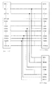
ここで、メインパネルの配線抵抗は、サブパネルを接続したメインパネルの配線抵抗R2より、計算式のとおりにR1の配線抵抗を大きくすることで理論的に設計することができる。メインパネルの配線抵抗値は、領域毎に全て同一の抵抗にならない場合がある。つまり、メインパネルのみ駆動している配線抵抗値もコントラストムラとして見えない範囲で段階的に徐々に変化していることもある。そのような場合には、メインパネルのみ駆動している領域とサブパネルと接続して駆動している領域の境界同士の抵抗値を考えればよい。このように設計することで、コントラストムラを理論的には解決することが可能である。
更に上記ダミーと接続した表示画面までの配線抵抗値は、第一の表示パネルのみ駆動する配線抵抗値と第一の表示パネルと第二の表示パネルを駆動する配線抵抗値との差をダミーの容量との増減は逆に段階的に変えた構成にした。
2 サブパネル
3 ドライバIC
4 第一のFPC
5 第二のFPC
6 バックライト
10 メインパネルと接続するための第一の接続端子群
11 サブパネルと接続するための第二の接続端子群
Claims (5)
- 第一表示パネルと、
前記第一表示パネルより表示画素数が少ない第二表示パネルと、
前記第一表示パネル及び前記第二表示パネルの表示画素に画像を表示させるための共通駆動信号と、前記第一表示パネルの表示画素のみに画像を表示させるための駆動信号を出力するドライバICと、を備える表示装置であって、
前記第一表示パネルの表示画面は、前記共通駆動信号が供給される第一ライン電極と前記駆動信号が供給される第二ライン電極で構成され、
前記第二表示パネルの表示画面は、前記共通駆動信号が供給される第一ライン電極で構成され、
前記第二表示パネルには、表示画面の外側に前記第一ライン電極と隣接して複数本のダミー電極が設けられ、
前記複数本のダミー電極は、表示画面から離れるにつれて、前記第二表示パネルの第一ライン電極の面積より面積が段々と小さくなるように形成され、
表示画面に近いダミー電極ほど、前記第一表示パネルの第一ライン電極に近い第二ライン電極の駆動信号が供給されることを特徴とする表示装置。 - 第一表示パネルと、前記第一表示パネルより表示画素数が少ない第二表示パネルと、
前記第一表示パネル及び前記第二表示パネルの表示画素に画像を表示させるための共通駆動信号と前記第一表示パネルの表示画素のみに画像を表示させるための駆動信号を出力するドライバICと、を備える表示装置であって、
前記第一表示パネルの表示画面は、前記共通駆動信号が供給される第一ライン電極と前記駆動信号が供給される第二ライン電極で構成され、
前記第二表示パネルの表示画面は、前記共通駆動信号が供給される第一ライン電極で構成され、
前記第一表示パネルにおいて、前記ドライバICから前記第二ライン電極までの配線は前記ドライバICから前記第一ライン電極までの配線より、抵抗が大きいことを特徴とする表示装置。 - 前記第二表示パネルには、表示画面の外側に前記第一ライン電極と隣接して複数本のダミー電極が設けられ、
前記複数本のダミー電極は、表示画面から離れるにつれて、前記第二表示パネルの前記第一ライン電極の面積より面積が段々と小さくなるとともに、
前記第一表示パネルにおいて、前記第一表示パネルの前記第一ライン電極に近いほど、前記ドライバICから前記第二ライン電極までの配線は、抵抗が小さくなるように形成されたことを特徴とする請求項2に記載の表示装置。 - 第一表示パネルと、前記第一表示パネルより表示画素数が少ない第二表示パネルと、
前記第一表示パネル及び前記第二表示パネルの表示画素に画像を表示させるための共通駆動信号と前記第一表示パネルの表示画素のみに画像を表示させるための駆動信号を出力するドライバICと、を備える表示装置であって、
前記第一表示パネルの表示画面は、前記共通駆動信号が供給される第一ライン電極と前記駆動信号が供給される第二ライン電極で構成され、
前記第二表示パネルの表示画面は、前記共通駆動信号が供給される第一ライン電極で構成され、
前記第二表示パネルには、前記第二表示パネルの前記第一ライン電極と表示画面の外側で隣接する一本のダミー電極が設けられ、
前記ダミー電極は、前記第二表示パネルの前記第一ライン電極の面積の約1/2であって、
前記第一表示パネルにおいて、前記ダミー電極に供給される前記駆動信号と同一の信号が供給された前記第二ライン電極から前記ドライバICまでの配線は、前記第一ライン電極から前記ドライバICまでの配線の抵抗値と、前記ダミー電極に供給される前記駆動信号と異なる信号が供給された前記第二ライン電極から前記ドライバICまでの配線の抵抗値との、中間の抵抗値を持つことを特徴とする表示装置。 - 前記ドライバICは、同一のセグメント信号と同一のコモン信号を前記第一表示パネルと前記第二表示パネルに同時に出力するとともに、
前記駆動信号と前記共通駆動信号は、前記コモン信号と前記セグメント信号の少なくとも一方の信号であることを特徴とする請求項1〜4のいずれか一項に記載の表示装置。
Priority Applications (2)
| Application Number | Priority Date | Filing Date | Title |
|---|---|---|---|
| JP2005051310A JP4767554B2 (ja) | 2004-07-13 | 2005-02-25 | 表示装置 |
| US11/178,746 US20060012539A1 (en) | 2004-07-13 | 2005-07-11 | Display device |
Applications Claiming Priority (3)
| Application Number | Priority Date | Filing Date | Title |
|---|---|---|---|
| JP2004205384 | 2004-07-13 | ||
| JP2004205384 | 2004-07-13 | ||
| JP2005051310A JP4767554B2 (ja) | 2004-07-13 | 2005-02-25 | 表示装置 |
Publications (3)
| Publication Number | Publication Date |
|---|---|
| JP2006053521A JP2006053521A (ja) | 2006-02-23 |
| JP2006053521A5 JP2006053521A5 (ja) | 2008-03-27 |
| JP4767554B2 true JP4767554B2 (ja) | 2011-09-07 |
Family
ID=35598916
Family Applications (1)
| Application Number | Title | Priority Date | Filing Date |
|---|---|---|---|
| JP2005051310A Expired - Fee Related JP4767554B2 (ja) | 2004-07-13 | 2005-02-25 | 表示装置 |
Country Status (2)
| Country | Link |
|---|---|
| US (1) | US20060012539A1 (ja) |
| JP (1) | JP4767554B2 (ja) |
Families Citing this family (6)
| Publication number | Priority date | Publication date | Assignee | Title |
|---|---|---|---|---|
| TWI274305B (en) * | 2006-04-04 | 2007-02-21 | Richtek Technology Corp | Double sided plate module of organic light-emitting diode |
| JP5020534B2 (ja) * | 2006-04-28 | 2012-09-05 | 京セラディスプレイ株式会社 | 表示パネル |
| US20100127962A1 (en) * | 2008-11-25 | 2010-05-27 | Ting-Yun Huang | Liquid Crystal Display Monitor |
| JP5407599B2 (ja) * | 2009-07-01 | 2014-02-05 | パナソニック株式会社 | タッチパネル |
| JP2012150152A (ja) * | 2011-01-17 | 2012-08-09 | Renesas Electronics Corp | データ処理装置及び半導体装置 |
| CN102333136B (zh) * | 2011-09-28 | 2014-03-26 | 东莞市亚星半导体有限公司 | 一种双屏手机 |
Family Cites Families (9)
| Publication number | Priority date | Publication date | Assignee | Title |
|---|---|---|---|---|
| JP4178870B2 (ja) * | 2001-09-21 | 2008-11-12 | セイコーエプソン株式会社 | 電気光学パネル、電気光学装置及び電子機器 |
| JP2003098540A (ja) * | 2001-09-26 | 2003-04-03 | Sharp Corp | 表示装置 |
| JP2003295218A (ja) * | 2002-04-04 | 2003-10-15 | Advanced Display Inc | 表示装置 |
| JP3854905B2 (ja) * | 2002-07-30 | 2006-12-06 | 株式会社 日立ディスプレイズ | 液晶表示装置 |
| JP4145637B2 (ja) * | 2002-11-25 | 2008-09-03 | シャープ株式会社 | アクティブマトリクス基板及び表示装置 |
| JP3976688B2 (ja) * | 2003-02-05 | 2007-09-19 | Nec液晶テクノロジー株式会社 | 液晶表示装置及びその製造方法 |
| JP4357188B2 (ja) * | 2003-02-28 | 2009-11-04 | 株式会社 日立ディスプレイズ | 液晶表示装置 |
| JP4492921B2 (ja) * | 2003-06-30 | 2010-06-30 | オプトレックス株式会社 | 液晶表示素子 |
| KR100957574B1 (ko) * | 2003-09-17 | 2010-05-11 | 삼성전자주식회사 | 표시장치 |
-
2005
- 2005-02-25 JP JP2005051310A patent/JP4767554B2/ja not_active Expired - Fee Related
- 2005-07-11 US US11/178,746 patent/US20060012539A1/en not_active Abandoned
Also Published As
| Publication number | Publication date |
|---|---|
| JP2006053521A (ja) | 2006-02-23 |
| US20060012539A1 (en) | 2006-01-19 |
Similar Documents
| Publication | Publication Date | Title |
|---|---|---|
| CN107424551B (zh) | 阵列基板、异形显示器及显示装置 | |
| JP5414974B2 (ja) | 液晶表示装置 | |
| TWI519857B (zh) | 顯示裝置及電子設備 | |
| JP2005292831A (ja) | 液晶表示装置 | |
| JP4767554B2 (ja) | 表示装置 | |
| JP5128703B2 (ja) | Tft基板及びこれを用いた液晶表示装置 | |
| KR101340670B1 (ko) | 액정표시장치 | |
| KR101100883B1 (ko) | 박막 트랜지스터 표시판 | |
| KR101323813B1 (ko) | 액정 표시 장치 | |
| US20060132425A1 (en) | Display device | |
| US20060001819A1 (en) | Display device | |
| US8937699B2 (en) | Liquid crystal display | |
| US8384704B2 (en) | Liquid crystal display device | |
| US10847109B2 (en) | Active matrix substrate and display panel | |
| JP4542202B2 (ja) | 表示装置 | |
| JP4163611B2 (ja) | 液晶表示装置 | |
| JP4133891B2 (ja) | 液晶表示装置とその製造方法 | |
| US10176779B2 (en) | Display apparatus | |
| JP6602136B2 (ja) | 表示装置 | |
| JP4541734B2 (ja) | 表示装置 | |
| JP2008309884A (ja) | 液晶表示装置 | |
| US10620734B2 (en) | Touch-panel-equipped display device | |
| JP2011164236A (ja) | 表示装置 | |
| KR20050007115A (ko) | 티.에프.티. 표시장치 | |
| US20180357973A1 (en) | Array substrate, display device and driving method thereof |
Legal Events
| Date | Code | Title | Description |
|---|---|---|---|
| A521 | Written amendment |
Free format text: JAPANESE INTERMEDIATE CODE: A523 Effective date: 20080212 |
|
| A621 | Written request for application examination |
Free format text: JAPANESE INTERMEDIATE CODE: A621 Effective date: 20080212 |
|
| RD01 | Notification of change of attorney |
Free format text: JAPANESE INTERMEDIATE CODE: A7421 Effective date: 20091105 |
|
| RD01 | Notification of change of attorney |
Free format text: JAPANESE INTERMEDIATE CODE: A7421 Effective date: 20091112 |
|
| A131 | Notification of reasons for refusal |
Free format text: JAPANESE INTERMEDIATE CODE: A131 Effective date: 20110322 |
|
| A521 | Written amendment |
Free format text: JAPANESE INTERMEDIATE CODE: A523 Effective date: 20110519 |
|
| TRDD | Decision of grant or rejection written | ||
| A01 | Written decision to grant a patent or to grant a registration (utility model) |
Free format text: JAPANESE INTERMEDIATE CODE: A01 Effective date: 20110614 |
|
| A01 | Written decision to grant a patent or to grant a registration (utility model) |
Free format text: JAPANESE INTERMEDIATE CODE: A01 |
|
| A61 | First payment of annual fees (during grant procedure) |
Free format text: JAPANESE INTERMEDIATE CODE: A61 Effective date: 20110615 |
|
| R150 | Certificate of patent or registration of utility model |
Free format text: JAPANESE INTERMEDIATE CODE: R150 |
|
| FPAY | Renewal fee payment (event date is renewal date of database) |
Free format text: PAYMENT UNTIL: 20140624 Year of fee payment: 3 |
|
| LAPS | Cancellation because of no payment of annual fees |