JP4759944B2 - Method for manufacturing nonvolatile semiconductor memory device - Google Patents
Method for manufacturing nonvolatile semiconductor memory device Download PDFInfo
- Publication number
- JP4759944B2 JP4759944B2 JP2004200913A JP2004200913A JP4759944B2 JP 4759944 B2 JP4759944 B2 JP 4759944B2 JP 2004200913 A JP2004200913 A JP 2004200913A JP 2004200913 A JP2004200913 A JP 2004200913A JP 4759944 B2 JP4759944 B2 JP 4759944B2
- Authority
- JP
- Japan
- Prior art keywords
- film
- substrate
- memory cell
- peripheral circuit
- forming
- Prior art date
- Legal status (The legal status is an assumption and is not a legal conclusion. Google has not performed a legal analysis and makes no representation as to the accuracy of the status listed.)
- Expired - Fee Related
Links
Images


Classifications
-
- H—ELECTRICITY
- H10—SEMICONDUCTOR DEVICES; ELECTRIC SOLID-STATE DEVICES NOT OTHERWISE PROVIDED FOR
- H10B—ELECTRONIC MEMORY DEVICES
- H10B41/00—Electrically erasable-and-programmable ROM [EEPROM] devices comprising floating gates
- H10B41/40—Electrically erasable-and-programmable ROM [EEPROM] devices comprising floating gates characterised by the peripheral circuit region
-
- H—ELECTRICITY
- H01—ELECTRIC ELEMENTS
- H01L—SEMICONDUCTOR DEVICES NOT COVERED BY CLASS H10
- H01L21/00—Processes or apparatus adapted for the manufacture or treatment of semiconductor or solid state devices or of parts thereof
- H01L21/70—Manufacture or treatment of devices consisting of a plurality of solid state components formed in or on a common substrate or of parts thereof; Manufacture of integrated circuit devices or of parts thereof
- H01L21/71—Manufacture of specific parts of devices defined in group H01L21/70
- H01L21/76—Making of isolation regions between components
- H01L21/762—Dielectric regions, e.g. EPIC dielectric isolation, LOCOS; Trench refilling techniques, SOI technology, use of channel stoppers
- H01L21/76224—Dielectric regions, e.g. EPIC dielectric isolation, LOCOS; Trench refilling techniques, SOI technology, use of channel stoppers using trench refilling with dielectric materials
- H01L21/76229—Concurrent filling of a plurality of trenches having a different trench shape or dimension, e.g. rectangular and V-shaped trenches, wide and narrow trenches, shallow and deep trenches
-
- H—ELECTRICITY
- H01—ELECTRIC ELEMENTS
- H01L—SEMICONDUCTOR DEVICES NOT COVERED BY CLASS H10
- H01L27/00—Devices consisting of a plurality of semiconductor or other solid-state components formed in or on a common substrate
- H01L27/02—Devices consisting of a plurality of semiconductor or other solid-state components formed in or on a common substrate including semiconductor components specially adapted for rectifying, oscillating, amplifying or switching and having at least one potential-jump barrier or surface barrier; including integrated passive circuit elements with at least one potential-jump barrier or surface barrier
- H01L27/04—Devices consisting of a plurality of semiconductor or other solid-state components formed in or on a common substrate including semiconductor components specially adapted for rectifying, oscillating, amplifying or switching and having at least one potential-jump barrier or surface barrier; including integrated passive circuit elements with at least one potential-jump barrier or surface barrier the substrate being a semiconductor body
- H01L27/10—Devices consisting of a plurality of semiconductor or other solid-state components formed in or on a common substrate including semiconductor components specially adapted for rectifying, oscillating, amplifying or switching and having at least one potential-jump barrier or surface barrier; including integrated passive circuit elements with at least one potential-jump barrier or surface barrier the substrate being a semiconductor body including a plurality of individual components in a repetitive configuration
- H01L27/105—Devices consisting of a plurality of semiconductor or other solid-state components formed in or on a common substrate including semiconductor components specially adapted for rectifying, oscillating, amplifying or switching and having at least one potential-jump barrier or surface barrier; including integrated passive circuit elements with at least one potential-jump barrier or surface barrier the substrate being a semiconductor body including a plurality of individual components in a repetitive configuration including field-effect components
-
- H—ELECTRICITY
- H10—SEMICONDUCTOR DEVICES; ELECTRIC SOLID-STATE DEVICES NOT OTHERWISE PROVIDED FOR
- H10B—ELECTRONIC MEMORY DEVICES
- H10B41/00—Electrically erasable-and-programmable ROM [EEPROM] devices comprising floating gates
- H10B41/40—Electrically erasable-and-programmable ROM [EEPROM] devices comprising floating gates characterised by the peripheral circuit region
- H10B41/42—Simultaneous manufacture of periphery and memory cells
- H10B41/43—Simultaneous manufacture of periphery and memory cells comprising only one type of peripheral transistor
- H10B41/44—Simultaneous manufacture of periphery and memory cells comprising only one type of peripheral transistor with a control gate layer also being used as part of the peripheral transistor
-
- H—ELECTRICITY
- H10—SEMICONDUCTOR DEVICES; ELECTRIC SOLID-STATE DEVICES NOT OTHERWISE PROVIDED FOR
- H10B—ELECTRONIC MEMORY DEVICES
- H10B43/00—EEPROM devices comprising charge-trapping gate insulators
- H10B43/30—EEPROM devices comprising charge-trapping gate insulators characterised by the memory core region
-
- H—ELECTRICITY
- H10—SEMICONDUCTOR DEVICES; ELECTRIC SOLID-STATE DEVICES NOT OTHERWISE PROVIDED FOR
- H10B—ELECTRONIC MEMORY DEVICES
- H10B99/00—Subject matter not provided for in other groups of this subclass
Description
本発明は、不揮発性半導体記憶装置及びその製造方法に係り、特にメモリセルに隣接する周辺回路の素子分離におけるエッチング残渣の発生防止に関するものである。 The present invention relates to a nonvolatile semiconductor memory device and a method for manufacturing the same, and more particularly to prevention of generation of etching residue in element isolation of a peripheral circuit adjacent to a memory cell.
不揮発性半導体記憶装置のメモリセルのカップリング比を向上させる方法が提案されている(例えば、特許文献1参照)。 A method for improving the coupling ratio of a memory cell of a nonvolatile semiconductor memory device has been proposed (see, for example, Patent Document 1).
また、公知技術ではなく、出願人が知っているメモリセルのカップリング比を向上させる方法として、素子分離としての分離酸化膜を所定の厚さだけエッチングすることによりコントロール電極の側面を露出させて、コントロールゲート電極に対向するフローティングゲート電極の表面積を増大させる方法がある。以下、この方法について説明する。 In addition, as a method for improving the coupling ratio of the memory cell known to the applicant, which is not a known technique, the side surface of the control electrode is exposed by etching the isolation oxide film as element isolation by a predetermined thickness. There is a method of increasing the surface area of the floating gate electrode facing the control gate electrode. Hereinafter, this method will be described.
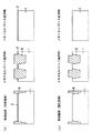
図17〜図24は、従来の不揮発性半導体記憶装置の製造方法を説明するための工程断面図である。
先ず、図17(a)に示すように、シリコン基板1上に熱酸化膜2を形成し、熱酸化膜2上にシリコン窒化膜3を形成する。さらに、シリコン窒化膜3上に、素子分離領域に対応する部分が開口するレジストパターン4を写真製版により形成する。
17 to 24 are process cross-sectional views for explaining a conventional method for manufacturing a nonvolatile semiconductor memory device.
First, as shown in FIG. 17A, a
次に、レジストパターン4をマスクとして、シリコン窒化膜3及び熱酸化膜2を順次ドライエッチングする。その後、レジストパターン4を除去する。続いて、パターニングされたシリコン窒化膜3をマスクとして、シリコン基板1をエッチングする。これにより、図17(b)に示すように、シリコン基板1内にトレンチ5が形成される。
Next, the
次に、トレンチ5内壁に熱酸化膜(図示せず)を形成し、その後、図18(a)に示すように、基板1全面に分離酸化膜となるシリコン酸化膜6を形成する。次に、図18(b)に示すように、シリコン窒化膜3をストッパ膜としてシリコン酸化膜6をCMP法により平坦化する。
Next, a thermal oxide film (not shown) is formed on the inner wall of the trench 5, and then, as shown in FIG. 18A, a
次に、シリコン窒化膜3を熱リン酸により除去すると、図19(a)に示す構造が得られる。さらに、熱酸化膜2をフッ酸により除去すると、図19(b)に示す構造が得られる。図25は、メモリセルアレイにおける活性領域を示す上面図である。図25に示すように、短冊状の活性領域Aがその短手方向に複数並んで形成されている。この活性領域Aを分離するように、素子分離としての分離酸化膜6が形成されている。
Next, when the
次に、図20(a)に示すように、基板1表面にトンネル酸化膜となる熱酸化膜7を形成し、基板1全面にメモリセルのフローティングゲート電極となるポリシリコン膜8を形成する。
Next, as shown in FIG. 20A, a
次に、図20(b)に示すように、分離酸化膜6をストッパ膜としてポリシリコン膜8をCMP法により平坦化する。これにより、シリコン酸化膜6の表面と、ポリシリコン膜8の表面が同じ高さになる。ここで、ポリシリコン膜8は、分離酸化膜6に対して自己整合的に位置決めされる。
Next, as shown in FIG. 20B, the
次に、図21(a)に示すように、分離酸化膜6をフッ酸により所定の膜厚だけ選択的にエッチングする。これにより、ポリシリコン膜8の側面上部が露出し、コントロールゲート電極に対向するフローティングゲート電極8の表面積を増大させることができ、メモリセルのカップリング比を向上させることができる。
その後、図21(b)に示すように、基板1全面にONO膜10を形成する。
Next, as shown in FIG. 21A, the
Thereafter, an
次に、図22(a)に示すように、メモリセル領域を覆うレジストパターン11を写真製版により形成する。
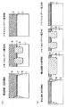
そして、図22(b)に示すように、レジストパターン11をマスクとして、周辺回路のONO膜10及びポリシリコン膜8を順次ドライエッチングする。さらに、周辺回路の熱酸化膜7をフッ酸により除去する。その後、レジストパターン11を除去すると、図23(a)に示す構造が得られる。ここで、図23(a)に示すように、周辺回路において、分離酸化膜6表面が基板1表面よりも落ち込むことにより段差Bが生じ、この段差Bに起因して後述する問題が発生する。
Next, as shown in FIG. 22A, a
Then, as shown in FIG. 22B, the ONO
次に、図23(b)に示すように、周辺回路において基板1表面にゲート酸化膜となる熱酸化膜12を形成する。そして、基板1全面に、メモリセルのコントロールゲート電極及び周辺回路のゲート電極となる導電膜としてのポリシリコン膜13及びWSi膜14を順次形成する。WSi膜14上にシリコン窒化膜15を形成し、シリコン窒化膜15上に、コントロールゲート電極部分及びゲート電極部分を覆うレジストパターン16を写真製版により形成する。
Next, as shown in FIG. 23B, a
次に、図24に示すように、レジストパターン16をマスクとしてシリコン窒化膜15をドライエッチングする。その後、レジストパターン16を除去する。続いて、パターニングされたシリコン窒化膜15をマスクとしてWSi膜14とポリシリコン膜13を順次ドライエッチングする。このとき、上述したように周辺回路の素子分離6上には段差Bが存在するため、この段差Bの部分にエッチング残渣(ポリシリコン残渣)13aが生じる可能性が高い。
Next, as shown in FIG. 24, the
上記製造方法では、メモリセルのカップリング比を向上させるために分離酸化膜6をエッチングする際、周辺回路における分離酸化膜6もエッチングしていた。このため、周辺回路におけるONO膜10及び熱酸化膜7を除去する際に、分離酸化膜6がさらにエッチングされ、分離酸化膜6表面が基板1表面よりも大きく落ち込んでしまい、段差Bが生じてしまうという問題があった。このため、その後のゲート電極のパターニングを行う際に、この段差Bにエッチング残渣13aが生じてしまうという問題があった。この残渣13aを介して本来絶縁すべき回路要素が導通してしまい、回路不良が発生してしまう問題があった。
In the above manufacturing method, the
本発明は、上述のような課題を解決するためになされたもので、周辺回路の分離酸化膜上にエッチング残渣を発生させることなく、高いカップリング比を有するメモリセルを有する不揮発性半導体記憶装置を製造することを目的とする。 The present invention has been made to solve the above-described problems, and a nonvolatile semiconductor memory device having a memory cell having a high coupling ratio without generating an etching residue on an isolation oxide film of a peripheral circuit. It aims to manufacture.
本発明に係る不揮発性半導体記憶装置の製造方法は、メモリセルと、該メモリセルに隣接する周辺回路とを有する不揮発性半導体記憶装置の製造方法であって、
基板の活性領域を分離する素子分離であって、その上面が該基板の表面よりも高い素子分離を該基板に形成する工程と、
前記基板上にシリコン酸化膜を形成する工程と、
前記素子分離の間の前記シリコン酸化膜上にポリシリコン膜を自己整合的に形成する工程と、
前記周辺回路を覆う第1レジストパターンを形成した後、前記メモリセルにおける前記素子分離を所定の膜厚だけエッチングする工程と、
前記基板全面に多層絶縁膜を形成する工程と、
前記メモリセルを覆う第2レジストパターンを形成した後、前記周辺回路における前記多層絶縁膜と前記ポリシリコン膜と前記シリコン酸化膜とを除去する工程と、
前記周辺回路の前記基板上にゲート絶縁膜を形成する工程と、
前記基板の全面に導電膜を形成する工程と、
前記周辺回路及び前記メモリセルにおける前記導電膜をパターニングする工程と、
前記メモリセルにおいて、パターニングされた前記導電膜をマスクとして前記多層絶縁膜及び前記ポリシリコン膜をパターニングする工程とを含むことを特徴とするものである。
A method for manufacturing a nonvolatile semiconductor memory device according to the present invention is a method for manufacturing a nonvolatile semiconductor memory device having a memory cell and a peripheral circuit adjacent to the memory cell,
Element isolation for isolating the active region of the substrate, the process of forming an element isolation on the substrate whose upper surface is higher than the surface of the substrate ;
Forming a silicon oxide film before SL on the substrate,
Forming a polysilicon film on the silicon oxide film during the element isolation in a self-aligning manner;
Etching the element isolation in the memory cell by a predetermined film thickness after forming a first resist pattern covering the peripheral circuit;
Forming a multilayer insulating film on the entire surface of the substrate;
Forming a second resist pattern covering the memory cell, and then removing the multilayer insulating film, the polysilicon film, and the silicon oxide film in the peripheral circuit;
Forming a gate insulating film on the substrate of the peripheral circuit;
Forming a conductive film on the entire surface of the substrate;
Patterning the conductive film in the peripheral circuit and the memory cell;
The memory cell includes a step of patterning the multilayer insulating film and the polysilicon film using the patterned conductive film as a mask.
本発明は、以上説明したように、第1レジストパターンをマスクとしてメモリセルにおける素子分離のみをエッチングすることにより、周辺回路における多層絶縁膜とポリシリコン膜とシリコン酸化膜とを除去する際に、周辺回路の素子分離上に基板表面に対する段差の発生を抑制することができ、該段差にエッチング残渣が発生することを防止することができる。 As described above, the present invention removes the multilayer insulating film, the polysilicon film, and the silicon oxide film in the peripheral circuit by etching only the element isolation in the memory cell using the first resist pattern as a mask. Generation of a step with respect to the substrate surface can be suppressed on the element isolation of the peripheral circuit, and an etching residue can be prevented from being generated at the step.
以下、図面を参照して本発明の実施の形態について説明する。図中、同一または相当する部分には同一の符号を付してその説明を簡略化ないし省略することがある。 Embodiments of the present invention will be described below with reference to the drawings. In the drawings, the same or corresponding parts are denoted by the same reference numerals, and the description thereof may be simplified or omitted.
以下、図を参照して、本発明の実施の形態による不揮発性半導体記憶装置の製造方法を説明する。
図1〜図11は、本実施の形態による不揮発性半導体記憶装置の製造方法を説明するための工程断面図である。
各図において、周辺回路の活性領域の断面と、メモリセルのゲート幅方向及びゲート長方向の断面を示している。また、必要に応じて、周辺回路の素子分離領域の断面を示している。
A method for manufacturing a nonvolatile semiconductor memory device according to an embodiment of the present invention will be described below with reference to the drawings.
1 to 11 are process cross-sectional views for explaining the method of manufacturing the nonvolatile semiconductor memory device according to the present embodiment.
In each figure, a cross section of the active region of the peripheral circuit and a cross section of the memory cell in the gate width direction and the gate length direction are shown. Moreover, the cross section of the element isolation area | region of a peripheral circuit is shown as needed.
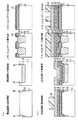
先ず、図1(a)に示すように、基板(例えばシリコン基板)1上にシリコン酸化膜(以下「熱酸化膜」という。)2を熱酸化法により、例えば10nm程度の膜厚で形成する。そして、熱酸化膜2上にシリコン窒化膜3をCVD法により、例えば100nm程度の膜厚で形成する。さらに、シリコン窒化膜3上に、活性領域に対応する部分を覆い、かつ、素子分離領域に対応する部分が開口するレジストパターン4を写真製版により形成する。
First, as shown in FIG. 1A, a silicon oxide film (hereinafter referred to as “thermal oxide film”) 2 is formed on a substrate (for example, a silicon substrate) 1 by a thermal oxidation method to a thickness of, for example, about 10 nm. . Then, a
次に、レジストパターン4をマスクとして、シリコン窒化膜3及び熱酸化膜2を順次ドライエッチングする。その後、レジストパターン4を除去する。続いて、パターニングされたシリコン窒化膜3をマスクとして、基板1をエッチングする。これにより、図1(b)に示すように、基板1内に200nm〜300nm程度の深さのトレンチ5が、シリコン窒化膜3の開口に連通して形成される。
Next, the
次に、図示しないが、トレンチ5の内壁に熱酸化膜を形成する。その後、図2(a)に示すように、基板1全面に分離酸化膜となるシリコン酸化膜6を、例えば500nm程度の膜厚で形成する。これにより、トレンチ5及びシリコン窒化膜3の開口がシリコン酸化膜6で埋め込まれる。
次に、図2(b)に示すように、シリコン窒化膜3をストッパ膜としてシリコン酸化膜6をCMP法により平坦化する。これにより、シリコン窒化膜3の表面と、シリコン酸化膜6の表面とが同じ高さになる。
次に、シリコン窒化膜3を熱リン酸により除去すると、図3(a)に示す構造が得られる。さらに、熱酸化膜2をフッ酸により除去すると、図3(b)に示す構造が得られる。これにより、上面が基板1表面よりも高い分離酸化膜6、すなわち基板1表面から上面が突き出た分離酸化膜6が形成される。図12は、メモリセルアレイにおける活性領域を示す上面図である。図12に示すように、短冊状の活性領域Aがその短手方向に複数並んで形成されており、活性領域Aを分離するように素子分離としての分離酸化膜6が形成されている。図25に示す従来のメモリセルアレイと異なり、本実施の形態ではメモリセルアレイの端部に活性領域A’が形成されたことにより、メモリセルアレイが活性領域A’により取り囲まれている。すなわち、メモリセルと周辺回路との境界部分に活性領域A’が形成されている。活性領域A’の周囲には周辺回路との素子分離が形成されている。このメモリセルアレイ端部に形成された活性領域A’は、短冊状の活性領域Aの端部を相互に接続する。活性領域A’の幅W1は、少なくとも短冊状の活性領域Aの幅W2よりも広い幅にする。なお、活性領域Aの端部には、ダミーゲート等を形成することができる。
Next, although not shown, a thermal oxide film is formed on the inner wall of the trench 5. Thereafter, as shown in FIG. 2A, a
Next, as shown in FIG. 2B, the
Next, when the
次に、図4(a)に示すように、基板1表面にトンネル酸化膜となるシリコン酸化膜7を熱酸化法により形成し、その後、メモリセルのフローティングゲート電極となるポリシリコン膜8を、例えば、150nm程度の膜厚で形成する。これにより、分離酸化膜6がポリシリコン膜8により覆われる。
次に、図4(b)に示すように、分離酸化膜6をストッパ膜としてポリシリコン膜8をCMP法により平坦化する。これにより、分離酸化膜6の表面と、ポリシリコン膜8の表面とが同じ高さになる。ここで、ポリシリコン膜8の位置は、分離酸化膜6に対して自己整合的に決められる。よって、フローティングゲート電極8が分離酸化膜6に対して自己整合的に形成されたことになり、写真製版を用いる場合に必要な分離酸化膜とフローティングゲート電極との高精度な位置合わせが不要になる。
Next, as shown in FIG. 4A, a
Next, as shown in FIG. 4B, the
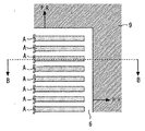
次に、図5(a)に示すように、周辺回路を覆うレジストパターン9を形成する。ここで、メモリセルアレイ端部に太い活性領域A’を形成することは上述したが(図12参照)、本工程では、図13及び図14に示すように、レジストパターン9端部が活性領域A’上に位置するように、レジストパターン9を配置する。これにより、メモリセルとの境界近傍の周辺回路における分離酸化膜6表面がレジストパターン9に覆われる。活性領域A’の幅W1は、レジストパターン9の重ね合わせ余裕や寸法バラツキを考慮した幅に設定し、必ずレジストパターン9端部が活性領域A’を踏み外さないようにする。
Next, as shown in FIG. 5A, a resist
次に、メモリセルにおける分離酸化膜6をフッ酸により所定の膜厚だけエッチングする。その後、レジストパターン9を除去すると、図5(b)に示す構造が得られる。分離酸化膜6のエッチングによりポリシリコン膜8の側面8aの一部が露出するため、コントロールゲート電極(後述)に対向するフローティングゲート電極8の表面積が増大し、メモリセルのカップリング比が向上する。このとき、周辺回路はレジストパターン9によりマスクされているため、周辺回路における分離酸化膜6はエッチングされない。
Next, the
次に、図6(a)に示すように、基板1全面に多層絶縁膜としてのONO膜10を形成する。ONO膜10は、シリコン酸化膜、シリコン窒化膜、シリコン酸化膜を積層した3層の絶縁膜である。なお、ONO膜10に代えて、シリコン酸化膜とシリコン窒化膜とを積層した2層の絶縁膜(ON膜又はNO膜)や、シリコン酸化膜とシリコン窒化膜とを交互に積層した4層の絶縁膜(ONON膜又はNONO膜)を形成することができる。
そして、メモリセル領域を覆い、かつ、周辺回路領域に対応する部分が開口するレジストパターン11を写真製版により形成する。
Next, as shown in FIG. 6A, an
Then, a resist
次に、図6(b)に示すように、周辺回路領域のONO膜9及びポリシリコン膜8を順次ドライエッチングする。続いて、周辺回路領域の熱酸化膜7をフッ酸により除去する。ここで、メモリセルにおける分離酸化膜6をエッチングする際、周辺回路の分離酸化膜6はレジストパターン9によりマスクされておりエッチングされていない。よって、この熱酸化膜7を除去する際、従来のように分離酸化膜6表面が基板1表面よりも落ち込まない。すなわち、通常のエッチング処理を行うことにより、図22(a)に示すような従来周辺回路に生じていた段差Bが、本発明では生じない。換言すれば、周辺回路の分離酸化膜6の上面が、基板1の表面と同等の高さであるか若しくは該表面よりも高い。
その後、レジストパターン11を除去する。
Next, as shown in FIG. 6B, the
Thereafter, the resist
次に、図7(a)に示すように、周辺回路にゲート絶縁膜となるシリコン酸化膜12を熱酸化法により、例えば15nm程度の膜厚で形成する。続いて、基板1全面に、メモリセルのコントロールゲート電極及び周辺回路のゲート電極となる導電膜としてポリシリコン膜13とタングステンシリサイド膜(以下「WSi膜」という。)14を積層する。さらに、WSi膜14上にシリコン窒化膜15を形成し、その上にメモリセルのコントロールゲート電極部分と、周辺回路のゲート電極部分とを覆うレジストパターン16を写真製版により形成する。
Next, as shown in FIG. 7A, a
次に、図7(b)に示すように、レジストパターン16をマスクとしてシリコン窒化膜15をドライエッチングする。その後、レジストパターン16を除去する。続いて、パターニングされたシリコン窒化膜15をマスクとしてWSi膜14とポリシリコン膜13を順次ドライエッチングする。これにより、メモリセルにコントロールゲート電極(13,14)が形成され、周辺回路にゲート電極(13,14)が形成される。このとき、上述したように周辺回路の分離酸化膜6上には段差が存在しないため、エッチング残渣の発生を抑制することができる。
Next, as shown in FIG. 7B, the
次に、周辺回路を覆うレジストパターンを写真製版により形成する。そして、パターニングされたシリコン窒化膜15、WSi膜14及びポリシリコン膜13をマスクとしてONO膜9及びポリシリコン膜8を順次ドライエッチングする。その後、イオン注入法によりメモリセルの基板1上層にソース/ドレイン領域18を形成する。続いて、レジストパターンを除去する。次に、ゲート側壁を熱酸化した後、基板全面にシリコン窒化膜19を形成すると、図8(a)に示す構造が得られる。
Next, a resist pattern covering the peripheral circuit is formed by photolithography. Then, the
次に、シリコン窒化膜19をエッチバックすることにより、ゲート電極側壁を覆うサイドウォール20が自己整合的に形成される。そして、メモリセルを覆うレジストパターンを写真製版により形成した後、イオン注入法により周辺回路の基板1上層にソース/ドレイン領域21を形成する。これにより、図8(b)に示すような構造が得られる。
Next, the
次に、図9に示すように、基板1全面に層間絶縁膜となるBPSG膜22を形成する。そして、BPSG膜22上にコンタクトホール形成部分が開口するレジストパターン23を写真製版により形成する。さらに、図10(a)に示すように、レジストパターン23をマスクとしてBPSG膜22をドライエッチングすることにより、ソース/ドレイン領域19に達するコンタクトホール24が形成される。その後、レジストパターン23を除去する。同様の手法で、図10(b)に示すように、ソース/ドレイン領域18,21に達するコンタクトホール25,26を形成する。なお、図1−図9におけるメモリセル(ゲート幅方向)断面はゲート電極部分の断面を示したが、図10−図11におけるメモリセル(ゲート幅方向)断面はコンタクト部分の断面を示す。
Next, as shown in FIG. 9, a
次に、基板1全面にタングステン膜を堆積し、BPSG膜22をストッパ膜としてCMP法による平坦化又はエッチバックを行う。これにより、図11(a)に示すように、コンタクトホール24,25,26内にタングステンプラグ27が形成される。
次に、BPSG膜22及びプラグ27上に層間絶縁膜としてのBPSG膜28を形成する。そして、BPSG膜28上にヴィアホール形成部分が開口するレジストパターンを写真製版により形成する。さらに、このレジストパターンをマスクとしてBPSG膜28をドライエッチングすることにより、所望のプラグ27に達するヴィアホールが形成される。その後、レジストパターンを除去する。続いて、基板1全面にタングステン膜を堆積し、BPSG膜28をストッパ膜としてCMP法による平坦化又はエッチバックを行うことにより、ヴィアホール内にタングステンプラグ29が形成される。最後に、タングステンプラグ29に接続されたアルミニウム配線30を形成する。これにより、図11(b)に示すような構造が得られる。
Next, a tungsten film is deposited on the entire surface of the
Next, a
以上説明したように、本実施の形態では、レジストパターン9をマスクとしてメモリセルにおける分離酸化膜6をエッチングすることにより、その後に周辺回路におけるONO膜10とポリシリコン膜8と熱酸化膜7を除去する際に、周辺回路の分離酸化膜6上に基板1表面に対する段差の発生を抑制することができる。よって、周辺回路の分離酸化膜6上にポリシリコン膜のエッチング残渣が発生することを防止でき、不揮発性半導体記憶装置の信頼性を向上させることができる。
As described above, in the present embodiment, by etching the
次に、上記実施の形態に対する比較例について説明する。
図15は、本比較例において、メモリセルの活性領域と、周辺回路を覆うレジストパターンとの位置関係を示す上面図である。
上記実施の形態では、図13及び図14に示すように、メモリセルアレイ端部を取り囲む活性領域A’上にレジストパターン9端部を配置した。これにより、メモリセルと周辺回路の境界部分の分離酸化膜6がエッチングされず、段差の発生を防止することができる。すなわち、上記実施の形態による方法を用いて製造された不揮発性半導体記憶装置において、メモリセルと周辺回路の境界部分の分離酸化膜6上面が、基板1の表面と同等の高さであるか若しくは該表面よりも高い。
これに対して、本比較例では、図15に示すように、短冊状活性領域Aの端部を接続する活性領域A’を形成せず、メモリセルと周辺回路の境界部分の分離酸化膜6上にレジストパターン9端部を配置した。この場合、図16に示すように、レジストパターン9で覆われていない部分の分離酸化膜6がエッチングされてしまい、その結果として段差Cが生じる。この段差Cに起因して、その後にメモリセルをマスクして行う周辺回路のONO膜9,ポリシリコン膜8,熱酸化膜7の除去によって、メモリセルと周辺回路の境界部分において従来周辺回路で発生したような分離酸化膜6上の段差が発生してしまう。
本実施の形態では、活性領域A’上にレジストパターン9端部を配置することにより、かかる段差Cの発生を防止することができる。このため、メモリセルと周辺回路の境界部分において分離酸化膜6上の段差の発生を防止することができ、さらにエッチング残渣の発生を防止することができる。
Next, a comparative example for the above embodiment will be described.
FIG. 15 is a top view showing the positional relationship between the active region of the memory cell and the resist pattern covering the peripheral circuit in this comparative example.
In the above embodiment, as shown in FIGS. 13 and 14, the end portion of the resist
On the other hand, in this comparative example, as shown in FIG. 15, the active region A ′ that connects the end portions of the strip-shaped active region A is not formed, and the
In the present embodiment, the step C can be prevented from occurring by disposing the end portion of the resist
1 基板(シリコン基板)、 2 熱酸化膜、 3 シリコン窒化膜、 4 レジストパターン、 5 トレンチ、 6 分離酸化膜(シリコン酸化膜)、 7 トンネル酸化膜(シリコン酸化膜)、 8 フローティングゲート電極(ポリシリコン膜)、 9 レジストパターン、 10 ONO膜、 11 レジストパターン、 12 ゲート絶縁膜(シリコン酸化膜)、 13 ポリシリコン膜、 14 WSi膜、 15 シリコン窒化膜、 16 レジストパターン、 19 シリコン窒化膜、 20 サイドウォール、 21 ソース/ドレイン領域、 22 層間絶縁膜(BPSG膜)、 23 レジストパターン、 24,25,26 コンタクトホール、 27 プラグ、 28 層間絶縁膜(BPSG膜)。 1 substrate (silicon substrate), 2 thermal oxide film, 3 silicon nitride film, 4 resist pattern, 5 trench, 6 isolation oxide film (silicon oxide film), 7 tunnel oxide film (silicon oxide film), 8 floating gate electrode (poly Silicon film), 9 resist pattern, 10 ONO film, 11 resist pattern, 12 gate insulating film (silicon oxide film), 13 polysilicon film, 14 WSi film, 15 silicon nitride film, 16 resist pattern, 19 silicon nitride film, 20 Sidewall, 21 source / drain region, 22 interlayer insulating film (BPSG film), 23 resist pattern, 24, 25, 26 contact hole, 27 plug, 28 interlayer insulating film (BPSG film).
Claims (2)
基板の活性領域を分離する素子分離であって、その上面が該基板の表面よりも高い素子分離を該基板に形成する工程と、
前記素子分離の間の前記基板上にシリコン酸化膜を形成する工程と、
前記素子分離の間の前記シリコン酸化膜上にポリシリコン膜を自己整合的に形成する工程と、
前記周辺回路を覆う第1レジストパターンを形成した後、前記メモリセルにおける前記素子分離を所定の膜厚だけエッチングする工程と、
前記基板全面に多層絶縁膜を形成する工程と、
前記メモリセルを覆う第2レジストパターンを形成した後、前記素子分離の表面を前記基板の表面よりも落ち込ませることなく、前記周辺回路における前記素子分離の上面を前記基板の表面と同等の高さとなるように若しくは前記基板の表面よりも高くなるように、前記周辺回路における前記多層絶縁膜と前記ポリシリコン膜と前記シリコン酸化膜とを除去する工程と、
前記周辺回路の前記基板上にゲート絶縁膜を形成する工程と、
前記基板の全面に導電膜を形成する工程と、
前記周辺回路及び前記メモリセルにおける前記導電膜をパターニングする工程と、
前記メモリセルにおいて、パターニングされた前記導電膜をマスクとして前記多層絶縁膜及び前記ポリシリコン膜をパターニングする工程とを含み、
前記メモリセルにおける活性領域は、短手方向に複数並んで配置された短冊状の第1活性領域と、該第1活性領域の端部を相互に接続すると共に前記メモリセルを取り囲むように配置された第2活性領域とを有し、
前記第1レジストパターンの端部が前記第2活性領域に位置するように前記第1レジストパターンを形成することを特徴とする不揮発性半導体記憶装置の製造方法。 A method for manufacturing a nonvolatile semiconductor memory device having a memory cell and a peripheral circuit adjacent to the memory cell,
Element isolation for isolating the active region of the substrate, the process of forming an element isolation on the substrate whose upper surface is higher than the surface of the substrate;
Forming a silicon oxide film on the substrate during the element isolation;
Forming a polysilicon film on the silicon oxide film during the element isolation in a self-aligning manner;
Etching the element isolation in the memory cell by a predetermined film thickness after forming a first resist pattern covering the peripheral circuit;
Forming a multilayer insulating film on the entire surface of the substrate;
After forming the second resist pattern covering the memory cell, the upper surface of the element isolation in the peripheral circuit is made to have the same height as the surface of the substrate without causing the surface of the element isolation to fall below the surface of the substrate. Removing the multilayer insulating film, the polysilicon film, and the silicon oxide film in the peripheral circuit so as to be higher than the surface of the substrate ,
Forming a gate insulating film on the substrate of the peripheral circuit;
Forming a conductive film on the entire surface of the substrate;
Patterning the conductive film in the peripheral circuit and the memory cell;
Patterning the multilayer insulating film and the polysilicon film using the patterned conductive film as a mask in the memory cell,
The active regions in the memory cell are arranged so that a plurality of strip-shaped first active regions arranged side by side in the short direction and ends of the first active regions are connected to each other and surround the memory cell. A second active region,
A method of manufacturing a nonvolatile semiconductor memory device, wherein the first resist pattern is formed so that an end portion of the first resist pattern is located in the second active region.
基板の活性領域を分離する素子分離であって、その上面が該基板の表面よりも高い素子分離を該基板に形成する工程と、
前記素子分離の間の前記基板上にトンネル酸化膜となるシリコン酸化膜を形成する工程と、
前記素子分離の間の前記シリコン酸化膜上にフローティングゲート電極となるポリシリコン膜を自己整合的に形成する工程と、
前記周辺回路を覆う第1レジストパターンを形成した後、前記メモリセルにおける前記素子分離を所定の膜厚だけエッチングすることにより、前記メモリセルにおける前記ポリシリコン膜の側面上部を露出させる工程と、
前記第1レジストパターンを除去した後、前記基板全面に多層絶縁膜を形成する工程と、
前記メモリセルを覆う第2レジストパターンを形成した後、前記素子分離の表面を前記基板の表面よりも落ち込ませることなく、前記周辺回路における前記素子分離の上面を前記基板の表面と同等の高さとなるように若しくは前記基板の表面よりも高くなるように、前記周辺回路における前記多層絶縁膜と前記ポリシリコン膜と前記シリコン酸化膜とを除去する工程と、
前記周辺回路における前記シリコン酸化膜を除去した後、周辺回路の前記基板上にゲート絶縁膜を形成する工程と、
前記基板の全面にゲート電極又はコントロールゲート電極となる導電膜を形成する工程と、
前記周辺回路及び前記メモリセルにおける前記導電膜をパターニングすることにより、前記周辺回路の前記ゲート絶縁膜上にゲート電極を形成すると共に、前記メモリセルの前記多層絶縁膜上にコントロールゲート電極を形成する工程と、
前記コントロールゲート電極をマスクとして前記メモリセルの前記多層絶縁膜及び前記ポリシリコン膜をパターニングすることにより、フローティングゲート電極を形成する工程とを含み、
前記メモリセルにおける活性領域は、短手方向に複数並んで配置された短冊状の第1活性領域と、該第1活性領域の端部を相互に接続すると共に前記メモリセルを取り囲むように配置された第2活性領域とを有し、
前記第1レジストパターンの端部が前記第2活性領域に位置するように前記第1レジストパターンを形成することを特徴とする不揮発性半導体記憶装置の製造方法。 A method for manufacturing a nonvolatile semiconductor memory device having a memory cell and a peripheral circuit adjacent to the memory cell,
Element isolation for isolating the active region of the substrate, the process of forming an element isolation on the substrate whose upper surface is higher than the surface of the substrate;
Forming a silicon oxide film to be a tunnel oxide film on the substrate during the element isolation;
Forming a polysilicon film to be a floating gate electrode on the silicon oxide film during the element isolation in a self-aligning manner;
Forming a first resist pattern covering the peripheral circuit, and then exposing the upper part of the side surface of the polysilicon film in the memory cell by etching the element isolation in the memory cell by a predetermined thickness;
Forming a multilayer insulating film on the entire surface of the substrate after removing the first resist pattern;
After forming the second resist pattern covering the memory cell, the upper surface of the element isolation in the peripheral circuit is made to have the same height as the surface of the substrate without causing the surface of the element isolation to fall below the surface of the substrate. Removing the multilayer insulating film, the polysilicon film, and the silicon oxide film in the peripheral circuit so as to be higher than the surface of the substrate ,
Forming a gate insulating film on the substrate of the peripheral circuit after removing the silicon oxide film in the peripheral circuit;
Forming a conductive film to be a gate electrode or a control gate electrode on the entire surface of the substrate;
By patterning the conductive film in the peripheral circuit and the memory cell, a gate electrode is formed on the gate insulating film of the peripheral circuit, and a control gate electrode is formed on the multilayer insulating film of the memory cell. Process,
Forming a floating gate electrode by patterning the multilayer insulating film and the polysilicon film of the memory cell using the control gate electrode as a mask,
The active regions in the memory cell are arranged so that a plurality of strip-shaped first active regions arranged side by side in the short direction and ends of the first active regions are connected to each other and surround the memory cell. A second active region,
A method of manufacturing a nonvolatile semiconductor memory device, wherein the first resist pattern is formed so that an end portion of the first resist pattern is located in the second active region.
Priority Applications (5)
| Application Number | Priority Date | Filing Date | Title |
|---|---|---|---|
| JP2004200913A JP4759944B2 (en) | 2004-07-07 | 2004-07-07 | Method for manufacturing nonvolatile semiconductor memory device |
| KR1020050059704A KR101148177B1 (en) | 2004-07-07 | 2005-07-04 | Method for manufacturing non-volatile semiconductor memory device, and non-volatile semiconductor memory device |
| US11/172,886 US7592226B2 (en) | 2004-07-07 | 2005-07-05 | Method for manufacturing non-volatile semiconductor memory device, and non-volatile semiconductor memory device |
| US12/537,652 US7829414B2 (en) | 2004-07-07 | 2009-08-07 | Method for manufacturing non-volatile semiconductor memory device, and non-volatile semiconductor memory device |
| US12/906,521 US8344473B2 (en) | 2004-07-07 | 2010-10-18 | Method for manufacturing non-volatile semiconductor memory device, and non-volatile semiconductor memory device |
Applications Claiming Priority (1)
| Application Number | Priority Date | Filing Date | Title |
|---|---|---|---|
| JP2004200913A JP4759944B2 (en) | 2004-07-07 | 2004-07-07 | Method for manufacturing nonvolatile semiconductor memory device |
Related Child Applications (1)
| Application Number | Title | Priority Date | Filing Date |
|---|---|---|---|
| JP2010079205A Division JP2010183098A (en) | 2010-03-30 | 2010-03-30 | Nonvolatile semiconductor memory device |
Publications (3)
| Publication Number | Publication Date |
|---|---|
| JP2006024705A JP2006024705A (en) | 2006-01-26 |
| JP2006024705A5 JP2006024705A5 (en) | 2007-08-02 |
| JP4759944B2 true JP4759944B2 (en) | 2011-08-31 |
Family
ID=35540423
Family Applications (1)
| Application Number | Title | Priority Date | Filing Date |
|---|---|---|---|
| JP2004200913A Expired - Fee Related JP4759944B2 (en) | 2004-07-07 | 2004-07-07 | Method for manufacturing nonvolatile semiconductor memory device |
Country Status (3)
| Country | Link |
|---|---|
| US (3) | US7592226B2 (en) |
| JP (1) | JP4759944B2 (en) |
| KR (1) | KR101148177B1 (en) |
Families Citing this family (11)
| Publication number | Priority date | Publication date | Assignee | Title |
|---|---|---|---|---|
| JP4759944B2 (en) * | 2004-07-07 | 2011-08-31 | ルネサスエレクトロニクス株式会社 | Method for manufacturing nonvolatile semiconductor memory device |
| KR100594326B1 (en) * | 2005-03-22 | 2006-06-30 | 삼성전자주식회사 | Non volatile memory device for 2 bit operation and manufacturing method therefor |
| US8183595B2 (en) * | 2005-07-29 | 2012-05-22 | International Rectifier Corporation | Normally off III-nitride semiconductor device having a programmable gate |
| WO2012071100A1 (en) * | 2010-09-08 | 2012-05-31 | William Marsh Rice University | Siox-based nonvolatile memory architecture |
| US8735863B2 (en) | 2011-01-28 | 2014-05-27 | Privatran | Integrated nonvolatile resistive memory elements |
| US9385163B2 (en) | 2011-08-26 | 2016-07-05 | William Marsh Rice University | Addressable SiOX memory array with incorporated diodes |
| JP2013135029A (en) * | 2011-12-26 | 2013-07-08 | Elpida Memory Inc | Semiconductor device manufacturing method |
| US9059094B2 (en) * | 2012-08-24 | 2015-06-16 | Macronix International Co., Ltd. | Semiconductor gate structure and method of fabricating thereof |
| US10071801B2 (en) * | 2013-08-13 | 2018-09-11 | The United States Of America As Represented By The Administrator Of Nasa | Tri-rotor aircraft capable of vertical takeoff and landing and transitioning to forward flight |
| US9425206B2 (en) * | 2014-12-23 | 2016-08-23 | Taiwan Semiconductor Manufacturing Co., Ltd. | Boundary scheme for embedded poly-SiON CMOS or NVM in HKMG CMOS technology |
| JP7117223B2 (en) * | 2018-11-08 | 2022-08-12 | ルネサスエレクトロニクス株式会社 | Semiconductor device manufacturing method |
Family Cites Families (9)
| Publication number | Priority date | Publication date | Assignee | Title |
|---|---|---|---|---|
| JP3710880B2 (en) | 1996-06-28 | 2005-10-26 | 株式会社東芝 | Nonvolatile semiconductor memory device |
| JP3540633B2 (en) * | 1998-11-11 | 2004-07-07 | 株式会社東芝 | Method for manufacturing semiconductor device |
| JP2001036048A (en) * | 1999-07-16 | 2001-02-09 | Denso Corp | Semiconductor memory and manufacture thereof |
| KR20010036048A (en) | 1999-10-05 | 2001-05-07 | 천경호 | Beverage composition for protection drunkage |
| JP4911826B2 (en) | 2001-02-27 | 2012-04-04 | ルネサスエレクトロニクス株式会社 | Nonvolatile semiconductor memory device and manufacturing method thereof |
| JP2003023115A (en) | 2001-07-06 | 2003-01-24 | Mitsubishi Electric Corp | Non-volatile semiconductor memory device and apparatus for manufacturing the same |
| JP4160283B2 (en) * | 2001-09-04 | 2008-10-01 | 株式会社東芝 | Manufacturing method of semiconductor device |
| JP2003289114A (en) * | 2002-03-28 | 2003-10-10 | Toshiba Corp | Semiconductor storage device and method for manufacturing the same |
| JP4759944B2 (en) * | 2004-07-07 | 2011-08-31 | ルネサスエレクトロニクス株式会社 | Method for manufacturing nonvolatile semiconductor memory device |
-
2004
- 2004-07-07 JP JP2004200913A patent/JP4759944B2/en not_active Expired - Fee Related
-
2005
- 2005-07-04 KR KR1020050059704A patent/KR101148177B1/en not_active IP Right Cessation
- 2005-07-05 US US11/172,886 patent/US7592226B2/en active Active
-
2009
- 2009-08-07 US US12/537,652 patent/US7829414B2/en active Active
-
2010
- 2010-10-18 US US12/906,521 patent/US8344473B2/en not_active Expired - Fee Related
Also Published As
| Publication number | Publication date |
|---|---|
| US7829414B2 (en) | 2010-11-09 |
| US20060006492A1 (en) | 2006-01-12 |
| KR101148177B1 (en) | 2012-05-24 |
| KR20060049817A (en) | 2006-05-19 |
| US8344473B2 (en) | 2013-01-01 |
| JP2006024705A (en) | 2006-01-26 |
| US20100219498A1 (en) | 2010-09-02 |
| US7592226B2 (en) | 2009-09-22 |
| US20110031580A1 (en) | 2011-02-10 |
Similar Documents
| Publication | Publication Date | Title |
|---|---|---|
| JP4947931B2 (en) | Semiconductor device | |
| KR101148177B1 (en) | Method for manufacturing non-volatile semiconductor memory device, and non-volatile semiconductor memory device | |
| JP2008078298A (en) | Semiconductor device and manufacturing method thereof | |
| JP4822792B2 (en) | Semiconductor device and manufacturing method thereof | |
| JP2008205379A (en) | Nonvolatile semiconductor memory and its production process | |
| JP2008047630A (en) | Semiconductor device and its manufacturing method | |
| JP2008091368A (en) | Semiconductor device and manufacturing method thereof | |
| US20080081463A1 (en) | Method for fabricating storage node contact in semiconductor device | |
| JP2004055826A (en) | Method for manufacturing semiconductor device | |
| JP2010183098A (en) | Nonvolatile semiconductor memory device | |
| JP2008192891A (en) | Semiconductor device and manufacturing method therefor | |
| KR100660548B1 (en) | Non-volatile memory device and method of forming the same | |
| JP2005294518A (en) | Semiconductor device and method for manufacturing the same | |
| KR101002519B1 (en) | Method of manufacturing a flash memory device | |
| JP2006196895A (en) | Forming method for self-aligned contact | |
| JP2005311166A (en) | Semiconductor memory device and method for manufacturing the same | |
| KR100506050B1 (en) | Contact formation method of semiconductor device | |
| KR101061171B1 (en) | Method of manufacturing semiconductor device | |
| KR100605102B1 (en) | Contact Plug Structure Of Semiconductor Device And Method Of Forming The Same | |
| JP2010034291A (en) | Method of manufacturing non-volatile semiconductor memory device | |
| KR20090009392A (en) | Method for manufacturing semiconductor device | |
| JP2008118025A (en) | Semiconductor device and method of manufacturing the same | |
| JP2008192890A (en) | Semiconductor device and manufacturing method thereof | |
| JP2010080602A (en) | Semiconductor apparatus and method of manufacturing the same | |
| JP2010080603A (en) | Method of manufacturing semiconductor device |
Legal Events
| Date | Code | Title | Description |
|---|---|---|---|
| A521 | Request for written amendment filed |
Free format text: JAPANESE INTERMEDIATE CODE: A523 Effective date: 20070618 |
|
| A621 | Written request for application examination |
Free format text: JAPANESE INTERMEDIATE CODE: A621 Effective date: 20070618 |
|
| A977 | Report on retrieval |
Free format text: JAPANESE INTERMEDIATE CODE: A971007 Effective date: 20100127 |
|
| A131 | Notification of reasons for refusal |
Free format text: JAPANESE INTERMEDIATE CODE: A131 Effective date: 20100202 |
|
| A521 | Request for written amendment filed |
Free format text: JAPANESE INTERMEDIATE CODE: A523 Effective date: 20100330 |
|
| A711 | Notification of change in applicant |
Free format text: JAPANESE INTERMEDIATE CODE: A712 Effective date: 20100521 |
|
| A131 | Notification of reasons for refusal |
Free format text: JAPANESE INTERMEDIATE CODE: A131 Effective date: 20101124 |
|
| A521 | Request for written amendment filed |
Free format text: JAPANESE INTERMEDIATE CODE: A523 Effective date: 20110119 |
|
| A02 | Decision of refusal |
Free format text: JAPANESE INTERMEDIATE CODE: A02 Effective date: 20110208 |
|
| A521 | Request for written amendment filed |
Free format text: JAPANESE INTERMEDIATE CODE: A523 Effective date: 20110331 |
|
| A911 | Transfer to examiner for re-examination before appeal (zenchi) |
Free format text: JAPANESE INTERMEDIATE CODE: A911 Effective date: 20110408 |
|
| TRDD | Decision of grant or rejection written | ||
| A01 | Written decision to grant a patent or to grant a registration (utility model) |
Free format text: JAPANESE INTERMEDIATE CODE: A01 Effective date: 20110510 |
|
| A61 | First payment of annual fees (during grant procedure) |
Free format text: JAPANESE INTERMEDIATE CODE: A61 Effective date: 20110523 |
|
| FPAY | Renewal fee payment (event date is renewal date of database) |
Free format text: PAYMENT UNTIL: 20140617 Year of fee payment: 3 |
|
| R150 | Certificate of patent or registration of utility model |
Free format text: JAPANESE INTERMEDIATE CODE: R150 Ref document number: 4759944 Country of ref document: JP Free format text: JAPANESE INTERMEDIATE CODE: R150 |
|
| S531 | Written request for registration of change of domicile |
Free format text: JAPANESE INTERMEDIATE CODE: R313531 |
|
| R350 | Written notification of registration of transfer |
Free format text: JAPANESE INTERMEDIATE CODE: R350 |
|
| LAPS | Cancellation because of no payment of annual fees |