JP4726187B2 - Semiconductor integrated circuit - Google Patents
Semiconductor integrated circuit Download PDFInfo
- Publication number
- JP4726187B2 JP4726187B2 JP2004344524A JP2004344524A JP4726187B2 JP 4726187 B2 JP4726187 B2 JP 4726187B2 JP 2004344524 A JP2004344524 A JP 2004344524A JP 2004344524 A JP2004344524 A JP 2004344524A JP 4726187 B2 JP4726187 B2 JP 4726187B2
- Authority
- JP
- Japan
- Prior art keywords
- access
- queue
- command
- memory
- selection
- Prior art date
- Legal status (The legal status is an assumption and is not a legal conclusion. Google has not performed a legal analysis and makes no representation as to the accuracy of the status listed.)
- Expired - Fee Related
Links
Images


Description
本発明は、複数の機能処理モジュールからアクセスされる内蔵メモリを搭載した半導体集積回路に関する。 The present invention relates to a semiconductor integrated circuits equipped with a built-in memory to be accessed from a plurality of functional modules.
近年、半導体プロセスの急速な進化に伴い、半導体集積回路に搭載できる回路の規模も増加し、多くの機能ブロックを搭載したLSIを設計することが可能である。また、内部の動作速度、最大クロック周波数の向上により高速動作も可能となり、益々高速、高性能化が進んでいる。 In recent years, with the rapid evolution of semiconductor processes, the scale of circuits that can be mounted on a semiconductor integrated circuit has increased, and it is possible to design an LSI having a large number of functional blocks. In addition, the internal operation speed and the maximum clock frequency are improved, so that high-speed operation is possible, and higher speed and higher performance are being promoted.
LSIに搭載される多くの機能処理ブロックは、外部メモリを参照することが一般的に行われている(例えば、特許文献1参照)。しかしながら、LSIから外部メモリを参照する際のアクセス速度の高速化は、LSI内部の高速化に比べて進歩が遅く、外部メモリへのアクセス速度がシステムのボトルネックとなることが予想されている。
外部メモリへのアクセス速度を上げる手法として、外部メモリのバス幅を広げる手法が挙げられる。しかしながら、外部メモリのバス幅を広げることはLSIの入出力(IO)数を増加させることとなる。 As a method for increasing the access speed to the external memory, there is a method for expanding the bus width of the external memory. However, increasing the bus width of the external memory increases the number of input / output (IO) of the LSI.
半導体プロセスの進化はLSI内部の集積度を大きく向上させているが、LSI外部のIOに関してはその利点を殆ど享受することができず、LSI内部の集積度を向上させたとしても、IO数を増加させるとIOネックとなり、結果として、LSIのダイサイズを小さくすることができず、半導体プロセスの進化による小型化が実現できない。 The evolution of the semiconductor process has greatly improved the integration level inside the LSI, but it can hardly enjoy the advantages of IO outside the LSI, and even if the integration level inside the LSI is improved, the number of IOs can be reduced. If it is increased, it becomes an IO neck, and as a result, the die size of the LSI cannot be reduced, and miniaturization due to the evolution of the semiconductor process cannot be realized.
また、LSI外部のIO数を増加させることは、LSIを実装するPCB基板上の配置/配線を複雑化するという問題もある。 Further, increasing the number of IOs outside the LSI has a problem that the arrangement / wiring on the PCB substrate on which the LSI is mounted becomes complicated.
一方、外部メモリを使用しない方法として、LSI内部に外部メモリと等しいメモリを実装する手法が提案されている。LSI内部に実装することで、メモリのバス幅を広げることができると共に外部に接続するメモリと比べてアクセス時間が短くなるため、高速なメモリへのアクセスが可能となる。 On the other hand, as a method not using an external memory, a method of mounting a memory equal to the external memory inside the LSI has been proposed. By mounting inside the LSI, the bus width of the memory can be widened and the access time is shortened compared to the memory connected to the outside, so that high-speed access to the memory becomes possible.
このLSI内部に搭載されるメモリとして、従来は内蔵SRAMが広く使用されてきたが、内蔵SRAMでは、サイズが大きく、大容量のメモリを搭載することは非常に困難であった。しかしながら、近年SRAMに対してサイズの小さい内蔵DRAMの技術が確立され、内蔵DRAMを使用することで大きな容量のメモリをLSI内部に搭載することが可能となっている。 Conventionally, a built-in SRAM has been widely used as a memory mounted in the LSI, but the built-in SRAM has a large size and it is very difficult to mount a large-capacity memory. However, in recent years, a technology for a built-in DRAM smaller in size than an SRAM has been established, and a large-capacity memory can be mounted inside an LSI by using the built-in DRAM.
大容量の内蔵メモリをLSI内部に搭載することにより、LSI内部に実装される各機能ブロックは広いバス幅でアクセスを発行し、広いメモリバンド幅を確保することが期待される。しかしながら、各機能処理ブロックが使用するメモリのビット構成は、ブロック毎に異なっている。つまり、各機能処理モジュールが使用するビット構成のメモリを実装する場合、そのビット構成毎の内蔵メモリを実装することになり、LSI内のレイアウトが複雑になる。また、各メモリマスタ同士で内蔵DRAMの共有化が図れないため、排他的に動作する機能処理モジュールが存在していたとしても、それぞれの機能処理ブロック毎に内蔵メモリが実装されているため、結果として、必要以上の容量の内蔵メモリが実装されることになる。 By mounting a large-capacity built-in memory inside the LSI, it is expected that each functional block mounted inside the LSI issues access with a wide bus width and secures a wide memory bandwidth. However, the bit configuration of the memory used by each function processing block is different for each block. That is, when a memory having a bit configuration used by each function processing module is mounted, a built-in memory for each bit configuration is mounted, and the layout in the LSI becomes complicated. In addition, since the built-in DRAM cannot be shared between the memory masters, even if there is a function processing module that operates exclusively, the built-in memory is mounted for each function processing block. As a result, a built-in memory having a capacity larger than necessary is mounted.
また、内蔵DRAMといった大容量の実装可能なメモリの場合、小容量での実装は困難であり、専用に内蔵DRAMを実装すると必要以上の容量の内蔵DRAMを搭載しなければならないという可能性があり、無駄な内蔵メモリを実装することになる。 In addition, in the case of a large-capacity mountable memory such as a built-in DRAM, it is difficult to mount in a small capacity, and if a built-in DRAM is mounted exclusively, there is a possibility that a built-in DRAM having an excessive capacity must be mounted. , Will be useless built-in memory.
反面、広いビット構成を使用する機能処理モジュールに合わせて、共有の内蔵メモリを実装する場合、全ての機能処理モジュールより広いビット幅単位でメモリアクセスが発行されることになる。そのため、狭いビット構成でアクセスする複数の機能処理モジュールが内蔵メモリへのアクセスを発行した場合でも、それらのメモリアクセスはシリアライズされることになり、システムとしての高速動作、並列動作を制限してしまう。 On the other hand, when a shared built-in memory is mounted in accordance with a function processing module that uses a wide bit configuration, memory access is issued in units of a wider bit width than all the function processing modules. Therefore, even when multiple function processing modules that access with a narrow bit configuration issue access to the built-in memory, those memory accesses will be serialized, limiting the high-speed operation and parallel operation of the system. .
本発明は、上述の課題を解決するためになされたもので、複数の機能処理モジュールが使用する内蔵メモリのアクセスバス幅が異なる場合であっても、効率的に内蔵メモリを共有可能とすることを目的とする。 The present invention has been made to solve the above-described problems, and enables the internal memory to be efficiently shared even when the access bus widths of the internal memories used by the plurality of function processing modules are different. With the goal.
内蔵メモリへアクセスする際のアクセスバス幅が異なる複数の機能処理モジュールからアクセスされ、前記複数の機能処理モジュールのアクセスバス幅のうちの最も小さいビット幅に相当するビット構成の内蔵メモリを、該アクセスバス幅のうちの最も大きいビット幅に相当するビット数を満たす個数分有する半導体集積回路であって、
前記内蔵メモリに対して設けられ、対応する内蔵メモリへのアクセスコマンドを保持する複数のコマンドキューと、
前記複数の機能処理モジュールから内蔵メモリに対するメモリアクセスの要求があると、当該メモリアクセスに対応するメモリアクセスコマンドを各機能処理モジュールにより要求された内蔵メモリに対する複数のコマンドキューの同一の段に入力するコマンド入力手段と、
前記複数のコマンドキューの先頭に保持されているメモリアクセスコマンドに基づいて複数の内蔵メモリに並列にアクセスする制御手段とを有することを特徴とする。
Access bus width for accessing the internal memory is accessed from different function processing module, the internal memory of the bit configuration corresponding to the smallest bit width of the access bus width of the plurality of functional modules, the access a semiconductor integrated circuit equivalent in number to the number meets the number of bits corresponding to the highest bit width of the bus width,
A plurality of command queues provided for the internal memory and holding access commands to the corresponding internal memory;
When there is a memory access request to the internal memory from the plurality of function processing modules, a memory access command corresponding to the memory access is input to the same stage of the plurality of command queues for the internal memory requested by each function processing module. Command input means;
And having a control means for accessing a parallel plurality of internal memory based on the memory access command held in the head of the plurality of command queues.
本発明によれば、複数の機能処理モジュールが使用する内蔵メモリのアクセスバス幅が異なる場合であっても、効率的に内蔵メモリを共有することができる。 According to the present invention, even when the access bus width of the built-in memory in which a plurality of function processing module uses different, efficiently built-in memory can Rukoto Yusuke co.
以下、図面を参照しながら発明を実施するための最良の形態について詳細に説明する。尚、本実施形態では、メモリへのアクセスビット幅が異なる複数の機能処理モジュールが半導体集積回路に接続され、各機能処理モジュールから内部に実装された内蔵メモリへのアクセスを並列に実現するシステムのメモリアクセス制御について説明する。 The best mode for carrying out the invention will be described below in detail with reference to the drawings. In the present embodiment, a plurality of function processing modules having different access bit widths to the memory are connected to the semiconductor integrated circuit, and access to the built-in memory mounted therein from each function processing module is realized in parallel. Memory access control will be described.
図1は、本実施形態におけるシステムの構成の一例を示す図である。図1に示すように、システムは、256ビット幅で内蔵メモリへアクセスする2つの機能処理回路MST0(117)及びMST1(118)と、512ビット幅で内蔵メモリへアクセスする2つの機能処理回路MST2(119)及びMST3(120)と、1024ビット幅で内蔵メモリへアクセスする2つの機能処理回路MST4(121)及びMST5(122)とを有する。また、本システムでは、内蔵メモリへのアクセスを発行する最小のビット幅が256ビットであり、最大のビット幅が1024ビットであるため、内蔵メモリとして、256ビット幅のRAM0(101)、RAM1(102)、RAM2(103)、RAM3(104)を4組搭載し、最大1024ビット幅のメモリを実現するものである。 FIG. 1 is a diagram illustrating an example of a system configuration according to the present embodiment. As shown in FIG. 1, the system has two function processing circuits MST0 (117) and MST1 (118) that access the built-in memory with a 256-bit width, and two function processing circuits MST2 that access the built-in memory with a 512-bit width. (119) and MST3 (120) and two function processing circuits MST4 (121) and MST5 (122) for accessing the built-in memory with a 1024-bit width. In this system, since the minimum bit width for issuing access to the internal memory is 256 bits and the maximum bit width is 1024 bits, the RAM0 (101) and RAM1 ( 102), 4 sets of RAM2 (103) and RAM3 (104) are mounted to realize a memory having a maximum width of 1024 bits.
尚、本実施形態では、各内蔵メモリの容量は1メガビット(Mbit)であり、合計4メガビットの内蔵メモリがシステム内に搭載されている。 In this embodiment, the capacity of each built-in memory is 1 megabit (Mbit), and a total of 4 megabits of built-in memory is mounted in the system.
それぞれの機能処理回路は、マルチプレクサ(MUX)を介してアクセスデコード回路(110)内のアクセスデコード機構に対してメモリアクセスを発行する。このアクセスデコード機構は機能処理回路のメモリアクセスビット幅構成毎に用意されており、本実施形態では、256ビット、512ビット、1024ビットの3構成の機能処理回路が存在し、各ビット幅構成に合わせて256ビット用のアクセスデコード機構0(113)と、512ビット用のアクセスデコード機構1(114)と、1024ビット用のアクセスデコード機構2(115)とを有する。 Each function processing circuit issues a memory access to the access decoding mechanism in the access decoding circuit (110) via the multiplexer (MUX). This access decoding mechanism is prepared for each memory access bit width configuration of the function processing circuit. In this embodiment, there are three function processing circuits of 256 bits, 512 bits, and 1024 bits. In addition, it has an access decode mechanism 0 (113) for 256 bits, an access decode mechanism 1 (114) for 512 bits, and an access decode mechanism 2 (115) for 1024 bits.
以下にアクセスデコード機構0〜2(113〜115)の機能について説明する。
The functions of the
アクセスデコード機構0〜2(113〜115)は、各機能処理回路からのメモリアクセスコマンドを受信し、アクセスするメモリに対するコマンドへと変換する。具体的には、書き込みアクセスか読み込みアクセスかの判定、各機能処理回路から発行されたメモリアドレスをデコードし、実装されるどのメモリのどの番地にアクセスするかのデコードを行う。アドレスのデコードに関しては、各アクセスデコード機構の司るバス幅に依存して変更される。
ここで、各メモリの取り扱うアドレス空間を図2に示す。各内蔵メモリは256ビット単位でアドレッシングされ、256ビット単位にアドレスが「1」加算される。アクセスデコード機構は、機能処理回路のアクセスビット幅に応じたアドレスに従ってアクセスを発行するメモリのアドレスへと変換する。 Here, the address space handled by each memory is shown in FIG. Each internal memory is addressed in units of 256 bits, and an address “1” is added in units of 256 bits. The access decoding mechanism converts into an address of a memory that issues access according to an address corresponding to the access bit width of the function processing circuit.
256ビットでアクセスが発行される機能処理回路の場合、内蔵メモリと同様に256ビット単位でアドレッシングされ、4メガビット空間をアクセスするために、アドレスとして[0000h]番地〜[3FFFh]番地までのアドレスを内蔵メモリのアドレスとしてマッピングする。その際、256ビット幅に対応したアドレス変換機構は[0000h]番地〜[0FFFh]番地までをRAM0(101)の空間、[1000h]番地〜[1FFFh]番地までをRAM1(102)の空間、[2000h]番地〜[2FFFh]番地までをRAM2(103)の空間、そして[3000h]番地〜[3FFFh]番地までをRAM3(104)の空間としてアドレスをデコードする。例えば、MST0(117)から[2400h]番地へのアクセスが発行されると、256ビット幅に対応したアクセスデコード機構0(113)はRAM2(103)の[0400h]番地へのアクセスを発行する。 In the case of a function processing circuit in which access is issued with 256 bits, the addresses from [0000h] to [3FFFh] are used as addresses in order to access a 4-megabit space as in the case of the built-in memory. Map as address of internal memory. At this time, the address conversion mechanism corresponding to the 256-bit width is the space from [0000h] to [0FFFh] in the RAM0 (101) space, the address from [1000h] to [1FFFh], the space in the RAM1 (102), [ Addresses are decoded using the space from the address 2000h] to address [2FFFh] in the RAM 2 (103) and the address from the address [3000h] to address [3FFFh] as the space in the RAM 3 (104). For example, when an access from the MST0 (117) to the [2400h] address is issued, the access decoding mechanism 0 (113) corresponding to the 256-bit width issues an access to the [0400h] address of the RAM2 (103).
図3は、256ビットに対応したアクセスデコード機構0(113)の構成を示す図である。まず、アクセスインターフェース(301)を介して機能処理回路からのアクセスを受け取り、アドレス、コマンドをバッファ(303)へと取り込む。そして、アドレスの上位2ビットをアクセス選択信号(302)としてDEMUX(304)へと入力する。このDEMUX(304)は下位12ビットのアドレス、コマンドをアクセス選択信号(302)が「00」の場合はRAM0(101)、「01」の場合はRAM1(102)、「10」の場合はRAM2(103)、「11」の場合はRAM3(104)へと振り分け、コマンドディスパッチャーCommand Dispatcher(111)へとコマンドを伝達する。 FIG. 3 is a diagram showing a configuration of the access decoding mechanism 0 (113) corresponding to 256 bits. First, an access from the function processing circuit is received via the access interface (301), and an address and a command are taken into the buffer (303). Then, the upper 2 bits of the address are input to the DEMUX (304) as an access selection signal (302). This DEMUX (304) is an address of lower 12 bits, and the command is RAM0 (101) when the access selection signal (302) is “00”, RAM1 (102) when “01”, and RAM2 when “10”. In the case of (103) and “11”, it is distributed to the RAM 3 (104), and the command is transmitted to the command dispatcher (Command Dispatcher (111)).
次に、512ビットでアクセスが発行される機能処理回路の場合、512ビット単位でアドレッシングされ、512ビット毎にアドレスが「1」加算される。4メガビット空間をアクセスするために、アドレスとして[0000h]番地〜[1FFFh]番地までのアドレスを内蔵メモリのアドレスとしてマッピングする。512ビット幅に対応したアクセスデコード機構1(114)は、512ビット幅の1回のアクセスに対して2つの内蔵メモリへのアクセスを発行する。その際、512ビット幅に対応したアドレス変換機構1(114)は、[0000h]番地〜[0FFFh]番地までをRAM0(101)及びRAM1(102)の空間、[1000h]番地〜[1FFFh]番地までをRAM2(103)及びRAM3(104)の空間としてアクセスを発行する。例えば、MST2(119)から[0A00h]番地へのアクセスが発行されると、512ビット幅に対応したアクセスデコード機構1(114)はRAM0(101)及びRAM1(102)双方の[0A00h]番地へのアクセスを発行する。 Next, in the case of a function processing circuit in which access is issued in 512 bits, addressing is performed in units of 512 bits, and an address is incremented by “1” for every 512 bits. In order to access the 4 megabit space, addresses from [0000h] to [1FFFh] are mapped as addresses in the built-in memory. The access decoding mechanism 1 (114) corresponding to the 512-bit width issues access to two built-in memories for one access having a 512-bit width. At that time, the address conversion mechanism 1 (114) corresponding to the 512-bit width is the space from the addresses [0000h] to [0FFFh] in the RAM0 (101) and RAM1 (102), the addresses [1000h] to [1FFFh]. The access is issued as the space of the RAM 2 (103) and the RAM 3 (104). For example, when access to address [0A00h] is issued from MST2 (119), access decode mechanism 1 (114) corresponding to the 512-bit width goes to addresses [0A00h] in both RAM0 (101) and RAM1 (102). Issuing access.
図4は、512ビットに対応したアクセスデコード機構1(114)の構成を示す図である。まず、アクセスインターフェース(401)を介して機能処理回路からのアクセスを受け取り、アドレス、コマンドをバッファ(403)へと取り込む。そして、アドレスの上位1ビットをアクセス選択信号(402)としてDEMUX(404)へと入力する。このDEMUX(404)は下位12ビットのアドレス、コマンドをアクセス選択信号(402)が「0」の場合はRAM0(101)及びRAM1(102)へのアクセス、「1」の場合はRAM2(103)及びRAM3(104)へのアクセスとして振り分け、コマンドディスパッチャーCommand Dispatcher(111)へとコマンドを伝達する。各アクセスは、コマンドディスパッチャー(111)の手前で分割される。 FIG. 4 is a diagram showing a configuration of the access decoding mechanism 1 (114) corresponding to 512 bits. First, an access from the function processing circuit is received via the access interface (401), and an address and a command are taken into the buffer (403). Then, the upper 1 bit of the address is input to the DEMUX (404) as the access selection signal (402). This DEMUX (404) is a low-order 12-bit address, a command accesses the RAM0 (101) and RAM1 (102) when the access selection signal (402) is “0”, and a RAM2 (103) when “1”. The command is distributed as access to the RAM 3 (104), and the command is transmitted to the command dispatcher (111). Each access is divided before the command dispatcher (111).
そして、1024ビットでアクセスが発行される機能処理回路の場合、1024ビット単位でアドレッシングされ、1024ビット毎にアドレスが「1」加算される。ここで、4メガビット空間をアクセスするために、アドレスとして[0000h]番地〜[0FFFh]番地までのアドレスを内蔵メモリのアドレスとしてマッピングする。1024ビット幅に対応したアクセスデコード機構2(115)は、1024ビット幅の1回のアクセスに対して4つの内蔵メモリへのアクセスを発行する。即ち、1回のアクセスに対してRAM0(101)、RAM1(102)、RAM2(103)、RAM3(104)へのアクセスを発行する。例えば、MST4(121)から[0800h]番地へとアクセスが発行されると、1024ビット幅に対応したアクセスデコード機構2(115)はRAM0(101)、RAM1(102)、RAM2(103)、RAM3(104)の全ての[0800h]番地へのアクセスを発行する。 In the case of a function processing circuit in which access is issued in 1024 bits, addressing is performed in units of 1024 bits, and the address is incremented by “1” for each 1024 bits. Here, in order to access the 4 megabit space, addresses from address [0000h] to [0FFFh] are mapped as addresses of the built-in memory. The access decoding mechanism 2 (115) corresponding to the 1024 bit width issues access to four internal memories for one access of 1024 bit width. That is, access to RAM0 (101), RAM1 (102), RAM2 (103), and RAM3 (104) is issued for one access. For example, when an access is issued from the MST4 (121) to the address [0800h], the access decoding mechanism 2 (115) corresponding to the 1024 bit width is RAM0 (101), RAM1 (102), RAM2 (103), RAM3. Issue access to all [0800h] addresses in (104).
図5は、1024ビットに対応したアクセスデコード機構2(115)の構成を示す図である。まず、アクセスインターフェース(501)を介して機能処理回路からのアクセスを受け取り、アドレス、コマンドをバッファ(502)へと取り込む。そして、バッファからそのままコマンドディスパッチャーCommand Dispatcher(111)へとコマンドを伝達する。各アクセスはコマンドディスパッチャー(111)の手前で分割される。 FIG. 5 is a diagram showing a configuration of the access decoding mechanism 2 (115) corresponding to 1024 bits. First, an access from the function processing circuit is received via the access interface (501), and an address and a command are taken into the buffer (502). Then, the command is transmitted as it is from the buffer to the command dispatcher Command Dispatcher (111). Each access is divided before the command dispatcher (111).
次に、コマンドディスパッチャー(111)は各ビット幅に対応したアクセスデコード機構0〜2(113〜115)からのアクセスを受け取ると共に、キュー制御回路(112)によりキューの状態を参照し、受け取ったアクセスをキューのどの段数に入力するかを指定する。
Next, the command dispatcher (111) receives access from the
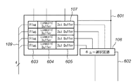
本実施形態では、コマンド発行機構(106)内に各内蔵メモリへのアクセスキュー(107)を有し、各内蔵メモリへのアクセスキュー(107)を4段とする。 In this embodiment, the command issuing mechanism (106) has an access queue (107) to each internal memory, and the access queue (107) to each internal memory has four stages.
図6は、本実施形態におけるアクセスキューの詳細な構成を示す図である。図6に示すように、アクセスキュー(107)は、キューフラグ(603)、コマンドバッファ(604)、データバッファ(605)で構成されている。また、キューフラグ(603)は1ビット、コマンドバッファ(604)は12ビットのアドレスと読み込み又は書き込み方向を示す1ビットのフラグの13ビット、データバッファ(605)は256ビットである。 FIG. 6 is a diagram showing a detailed configuration of the access queue in the present embodiment. As shown in FIG. 6, the access queue (107) is composed of a queue flag (603), a command buffer (604), and a data buffer (605). The queue flag (603) is 1 bit, the command buffer (604) is a 12-bit address and 13 bits of a 1-bit flag indicating the reading or writing direction, and the data buffer (605) is 256 bits.
図6に示す構成において、アクセスキュー(107)からは一番上位に格納されているコマンドが出力される。キューフラグ(603)は、その段に有効なコマンド、データが存在するか否かを示し、有効である場合は「1」、それ以外は「0」である。 In the configuration shown in FIG. 6, the command stored at the top is output from the access queue (107). The queue flag (603) indicates whether or not there is a valid command or data at that stage, and is “1” if it is valid, and “0” otherwise.
キュー選択回路(108)は、キュー指定信号(602)、アクセスコマンド、データ、アクセス有効信号を受け取り、キュー出力信号(601)を入力し、各キュー(107)へコマンド、データを出力する。キュー指定信号(602)、アクセスコマンド、データ、アクセス有効信号はアクセスデコード回路(110)より出力され、キュー指定信号(602)にてどのキューの段数にコマンド、データを入力するかが指定される。 The queue selection circuit (108) receives the queue designation signal (602), the access command, data, and the access valid signal, receives the queue output signal (601), and outputs the command and data to each queue (107). The queue designation signal (602), access command, data, and access valid signal are output from the access decode circuit (110), and the queue designation signal (602) designates to which queue stage the command and data are input. .
また、キュー選択回路(108)は、アクセス有効信号が有効を示す時に、キュー指定信号(602)とメモリ制御回路より発行されるキュー出力信号(601)とを参照し、キュー出力信号(601)が発行されていない場合はキュー指定信号(602)に示された段数に、キュー出力信号(601)が発行されている場合はキュー指定信号(602)で指定された段数より1つ進んだ段数にコマンド、データを出力する。 The queue selection circuit (108) refers to the queue designation signal (602) and the queue output signal (601) issued from the memory control circuit when the access valid signal indicates validity, and the queue output signal (601). Is not issued, the number of stages indicated by the queue designation signal (602), and when the queue output signal (601) is issued, the number of stages advanced by one from the number of stages designated by the queue designation signal (602) Command and data are output to.
例えば、キュー指定信号(602)が3段目を指定して、キュー出力信号(601)が発行されていない場合はコマンド、データを3段目に出力し、キュー出力信号(601)が発行されている場合はコマンド、データを2段目に出力するように制御する。 For example, when the queue designation signal (602) designates the third stage and the queue output signal (601) is not issued, the command and data are outputted to the third stage, and the queue output signal (601) is issued. If so, control is performed so that the command and data are output to the second stage.
アクセスキュー(107)は、キュー出力信号(601)が発行されると、1段目のコマンド、データ、キューフラグ(603)の値をメモリ制御回路(105)に出力する。また同時に、前段のコマンド、データ、或いはキュー選択回路(108)より出力されたコマンド、データを取り込む。後述するが、コマンドディスパッチャー(111)において空きキュー段に対してアクセスコマンド、データを発行するため、キュー内のデータの衝突は回避される。また、4段目のキューはキュー選択回路(108)からの入力がない場合、キューフラグ(603)を無効とし、コマンド、データに関しては処理を行わない。 When the queue output signal (601) is issued, the access queue (107) outputs the first stage command, data, and the value of the queue flag (603) to the memory control circuit (105). At the same time, the command and data output from the preceding stage command and data or the queue selection circuit (108) are fetched. As will be described later, since the command dispatcher (111) issues an access command and data to the empty queue stage, collision of data in the queue is avoided. Further, when there is no input from the queue selection circuit (108), the queue in the fourth stage invalidates the queue flag (603) and does not perform processing on commands and data.
また、キュー出力信号(601)が発行されていない場合は、各キュー段はキュー選択回路(108)よりコマンドの入力がない限りキューの情報を保持する。キュー選択回路(108)よりコマンド、データの入力がなされると、各キュー段はコマンドとデータを保持すると共にキューフラグ(603)を有効とする。 When the queue output signal (601) has not been issued, each queue stage holds queue information unless a command is input from the queue selection circuit (108). When a command and data are input from the queue selection circuit (108), each queue stage holds the command and data and validates the queue flag (603).
また、各段のキューフラグ(603)は、キュー状態信号(109)として出力され、各アクセスキュー(107)は4ビット、4組のキューで16ビットのキュー状態信号(109)をアクセスデコード回路(110)へと発行する。 In addition, the queue flag (603) of each stage is output as a queue status signal (109), and each access queue (107) is a 4-bit, 4 sets of queues, and a 16-bit queue status signal (109) is an access decoding circuit. Issue to (110).
アクセスデコード回路(110)内のコマンドディスパッチャー(111)は、発行されたキュー状態信号(109)を参照し、各コマンドをどのキューの段数へアクセスするかを決定する。 The command dispatcher (111) in the access decode circuit (110) refers to the issued queue status signal (109) to determine which queue stage number each command is accessed.
図8は、本実施形態におけるコマンドディスパッチャー(111)の構成の一例を示す図である。図8に示すように、コマンドディスパッチャー(111)は、キューの状態からキューへのコマンド発行を制御するキュー制御機構(112)とコマンド制御機構(116)とに分けられ、コマンド制御機構(116)は各内蔵メモリに対応したコマンド選択機構(801)と選択信号生成回路(805)とから構成されている。そして、キュー制御機構(112)は、キュー状態信号(109)より256ビット幅、512ビット幅、1024ビット幅のアクセスがキューの何段目に入ることができるかの選択信号を生成する。 FIG. 8 is a diagram showing an example of the configuration of the command dispatcher (111) in the present embodiment. As shown in FIG. 8, the command dispatcher (111) is divided into a queue control mechanism (112) and a command control mechanism (116) for controlling command issuance to the queue from the queue state, and the command control mechanism (116). Consists of a command selection mechanism (801) and a selection signal generation circuit (805) corresponding to each built-in memory. Then, the queue control mechanism (112) generates a selection signal as to which stage of the queue the access of 256 bits width, 512 bits width and 1024 bits width can enter from the queue status signal (109).
256ビット幅は各キューの空きで一番上位のものを指示し、512ビット幅はRAM0(101)、RAM1(102)又はRAM2(103)、RAM3(104)に対応するキューで双方のキューで同じ段数の空きで一番上位の者を指示し、1024ビット幅は全てのキューで同じ段数での空きで一番上位のものを指示し、選択信号としてコマンド選択機構(801)に対して発行する。 The 256-bit width indicates the highest available one in each queue, and the 512-bit width is a queue corresponding to RAM0 (101), RAM1 (102) or RAM2 (103), RAM3 (104). The highest rank is indicated with the same number of vacant spaces, and the 1024-bit width indicates the highest rank with the same number of tiers in all queues, and is issued to the command selection mechanism (801) as a selection signal. To do.
256ビット幅に対するキュー選択信号はRAM0(101)、RAM1(102)、RAM2(103)、RAM3(104)に対応して4組、また512ビット幅に対するキュー選択信号はRAM0(101)、RAM1(102)の組とRAM2(103)、RAM3(104)の組に対応して2組、更に1024ビット幅に対するキュー指定信号(806)は全ての内蔵メモリに対応して1組発行され、各コマンド選択機構(801)に出力される。 The queue selection signals for 256-bit width correspond to 4 sets corresponding to RAM0 (101), RAM1 (102), RAM2 (103), and RAM3 (104), and the queue selection signals for 512-bit width are RAM0 (101) and RAM1 ( 102) and 2 sets corresponding to the set of RAM2 (103) and RAM3 (104), and a queue designation signal (806) corresponding to the 1024 bit width is issued for each built-in memory. It is output to the selection mechanism (801).
各コマンド選択機構(801)は対応する内蔵メモリに応じた選択信号が256ビット幅、512ビット幅、1024ビット幅の3系統分入力される。 Each command selection mechanism (801) receives selection signals corresponding to the corresponding built-in memory for three systems of 256-bit width, 512-bit width, and 1024-bit width.
図7を用いてキュー制御機構の制御手法を示す。図の上辺から1段、2段、3段、4段とすると1段目はキューの先頭であり、4段目はキューの最後尾を示す。各キュー要素の中に示される「有効」のフラグは、そのキューの中に有効なメモリアクセスが入っていることを示しており、空欄のキュー要素には有効メモリアクセスコマンドが入っておらず、新たにメモリアクセスコマンドを挿入することが可能な状態であることを示している。 A control method of the queue control mechanism will be described with reference to FIG. If the first, second, third, and fourth levels from the top of the figure, the first level indicates the head of the queue, and the fourth level indicates the tail of the queue. The “valid” flag shown in each queue element indicates that there is valid memory access in the queue, and the empty queue element does not contain a valid memory access command. This indicates that a new memory access command can be inserted.
図7に示す状態をキュー状態信号(109)が示すとき、キュー制御機構(112)は、RAM0(101)に対応するコマンド選択機構(801)に対して256ビット幅系統のキュー指定信号(806)は4段目、512ビット幅系統のキュー指定信号(806)は4段目、1024ビット幅系統のキュー指定信号(806)は4段目を示している。 When the queue state signal (109) indicates the state shown in FIG. 7, the queue control mechanism (112) sends a 256-bit width queue designation signal (806) to the command selection mechanism (801) corresponding to the RAM0 (101). ) Indicates the fourth stage, the queue designation signal (806) of the 512-bit width system indicates the fourth stage, and the queue designation signal (806) of the 1024-bit width system indicates the fourth stage.
また、RAM1(102)に対応するコマンド選択機構(801)に対しては、256ビット系統のキュー指定信号(806)は1段目、512ビット、1024ビットはRAM0(101)に対応するコマンド選択機構(801)と同一の信号が示される。 For the command selection mechanism (801) corresponding to the RAM1 (102), the 256-bit queue designation signal (806) is the first stage, 512 bits, and 1024 bits are the command selection corresponding to the RAM0 (101). The same signal as mechanism (801) is shown.
更に、RAM2(103)に対応するコマンド選択機構(801)に対しては、256ビット幅系統のキュー指定信号(806)は3段目、512ビット幅のキュー指定信号(806)は3段目、1024ビット幅のキュー指定信号(806)はRAM0(101)、RAM1(102)に対応するコマンド選択機構(801)と同一の信号が示される。 Further, for the command selection mechanism (801) corresponding to the RAM 2 (103), the queue designation signal (806) of the 256-bit width system is the third stage, and the queue designation signal (806) of the 512-bit width is the third stage. The queue designation signal (806) having a width of 1024 bits indicates the same signal as that of the command selection mechanism (801) corresponding to the RAM0 (101) and the RAM1 (102).
更に、RAM3(104)に対応するコマンド選択機構(801)に対しては、256ビット幅系統のキュー指定信号(806)は1段目、512ビット幅、1024ビット幅のキュー指定信号(806)はRAM2(103)に対応するコマンド選択機構(801)と同一の信号が入力される。 Further, for the command selection mechanism (801) corresponding to the RAM3 (104), the queue designation signal (806) of the 256-bit width system is the first stage, 512-bit width, 1024-bit width queue designation signal (806). The same signal as that of the command selection mechanism (801) corresponding to the RAM 2 (103) is input.
コマンド選択機構(801)は、アクセスデコード機構0〜2(113〜115)で各内蔵メモリへと分配されたアクセスの入力と選択信号生成回路(805)からのアクセス選択信号(802,803,804)が入力される。アクセスの入力は、256ビット幅、512ビット幅、1024ビット幅それぞれからのアクセスが入力され、アクセス選択信号(802,803,804)によりコマンド選択機構(801)内で一つに選択される。選択信号生成回路(805)は、各コマンド選択機構(801)がどのアクセスデコード機構0〜2(113〜115)からのアクセスを取り込むかを決定するアクセス選択信号(802,803,804)を生成する。
The command selection mechanism (801) inputs the access distributed to each internal memory by the
図9は、本実施形態における選択信号生成回路(805)の構成の一例を示す図である。選択信号生成回路(805)の入力として、各内蔵メモリに対する4本の256ビット幅アクセス有効信号(903)、2本の512ビット幅アクセス有効信号(903)が入力される。6入力OR回路(901)の出力が1024ビット選択禁止信号(804)、RAM0(101)、RAM1(102)に対する256ビット幅アクセス有効信号(903)、2入力OR回路(902)の出力が512ビット選択禁止信号0(802)、RAM2(103)、RAM3(104)に対する512ビット幅アクセス有効信号(903)、2入力OR回路(902)の出力が512ビット選択禁止信号1(803)として出力される。1024ビット選択禁止信号(804)は全てのコマンド選択機構(801)へ出力され、512ビット選択禁止信号0(802)はRAM0(101)、RAM1(102)に対応するコマンド選択機構(801)へ、512ビット選択禁止信号1(803)はRAM2(103)、RAM3(104)に対応するコマンド選択機構(801)へと出力される。 FIG. 9 is a diagram illustrating an example of the configuration of the selection signal generation circuit (805) in the present embodiment. As inputs of the selection signal generation circuit (805), four 256-bit width access valid signals (903) and two 512-bit width access valid signals (903) for each built-in memory are input. The output of the 6-input OR circuit (901) is a 1024-bit selection inhibition signal (804), the 256-bit width access valid signal (903) for the RAM0 (101) and RAM1 (102), and the output of the 2-input OR circuit (902) is 512 Bit selection prohibition signal 0 (802), 512-bit access valid signal (903) for RAM2 (103), RAM3 (104), and output of 2-input OR circuit (902) are output as 512-bit selection prohibition signal 1 (803) Is done. The 1024-bit selection inhibition signal (804) is output to all command selection mechanisms (801), and the 512-bit selection inhibition signal 0 (802) is sent to the command selection mechanism (801) corresponding to RAM0 (101) and RAM1 (102). The 512-bit selection inhibition signal 1 (803) is output to the command selection mechanism (801) corresponding to the RAM2 (103) and RAM3 (104).
コマンド選択機構(801)では、1024ビット選択禁止信号(804)、512ビット選択禁止信号(802,803)をアクセス選択信号として入力し、1024ビット選択禁止信号(804)、512ビット選択禁止信号(802,803)の双方が有効の場合は256ビット幅のアクセスのみを受け付け、1024ビット選択禁止信号(804)のみの時は512ビット幅のアクセスのみを受け付け、双方共に無効の場合は1024ビット幅アクセスを受け付けることが可能とする。 In the command selection mechanism (801), a 1024-bit selection prohibition signal (804) and a 512-bit selection prohibition signal (802, 803) are input as an access selection signal, and a 1024-bit selection prohibition signal (804) and a 512-bit selection prohibition signal ( If both 802 and 803) are valid, only 256-bit width access is accepted. If only the 1024-bit selection prohibition signal (804) is accepted, only 512-bit width access is accepted. If both are invalid, 1024-bit width is accepted. It is possible to accept access.
コマンド選択機構(801)にて、256ビット幅、512ビット幅、1024ビット幅の中から選択されたアクセスは、キュー制御機構(112)により生成されたキュー指定信号(806)のうち、該当するビット幅のキュー段数を選択し、コマンド、データ、キュー指定信号(602)をアクセスキュー(107)へと発行する。 The access selected from the 256-bit width, 512-bit width, and 1024-bit width by the command selection mechanism (801) corresponds to the queue designation signal (806) generated by the queue control mechanism (112). The number of queue stages having a bit width is selected, and a command, data, and queue designation signal (602) are issued to the access queue (107).
アクセスキュー(107)は、対応するメモリ制御回路(105)と接続されている。各メモリ制御回路(105)は、アクセスを受信するタイミングでキューに対してキュー出力信号(601)を発行し、キューの先頭のコマンド、データ、キューフラグ(603)を受け取る。ここで、キューフラグ(603)が「1」を示していないときはアクセスがないと判定し、内蔵メモリへのアクセスを発行しない。一方、キューフラグ(603)が「1」を示しているときは、受け取ったコマンド、データに基づいてメモリアクセスを発行する。4組のメモリ制御回路(105)は同期して動作し、同一のサイクルタイミングでキュー出力信号(601)を発行する。本実施形態では、メモリ制御回路(105)のアクセス応答時間は3サイクルとする。 The access queue (107) is connected to the corresponding memory control circuit (105). Each memory control circuit (105) issues a queue output signal (601) to the queue at the timing of receiving access, and receives the command, data, and queue flag (603) at the head of the queue. Here, when the queue flag (603) does not indicate “1”, it is determined that there is no access, and access to the built-in memory is not issued. On the other hand, when the queue flag (603) indicates “1”, a memory access is issued based on the received command and data. The four sets of memory control circuits (105) operate synchronously and issue a queue output signal (601) at the same cycle timing. In this embodiment, the access response time of the memory control circuit (105) is 3 cycles.
以上の構成からなる本実施形態におけるシステムの動作について詳細に説明する。 The operation of the system in the present embodiment configured as described above will be described in detail.
図10は、本実施形態における各機能処理回路が発行するアクセスシーケンスの一例を示す図である。また図11は、本実施形態における各サイクルでのキュー状態を示す図である。 FIG. 10 is a diagram showing an example of an access sequence issued by each function processing circuit in the present embodiment. FIG. 11 is a diagram illustrating a queue state in each cycle in the present embodiment.
図10に示す「Issue」は、そのサイクルにおいて、機能処理回路がメモリアクセスを発行することを表している。 “Issue” shown in FIG. 10 indicates that the function processing circuit issues a memory access in the cycle.
まず、サイクル0では、MST0(117)が[0000h]番地、MST4(121)が[0100h]番地へのアクセスを発行する。これにより、アクセスデコード機構0,2(113,115)にてそれぞれのアクセスがデコードされ、MST0(117)のアクセスはRAM0(101)に対応したコマンド選択機構(801)へと伝達され、MST4(121)のアクセスは全てのコマンド選択機構(801)へと伝達される。この時、選択信号生成回路(805)では1024ビット選択禁止信号(804)と512ビット選択禁止信号(802,803)とが発行されているため、256ビット幅のMST0(117)のアクセスが選択され、図11に示す(A)のように、RAM0(101)に対応したキューの先頭に出力される。
First, in
次に、サイクル1において、MST2(119)が[1000h]番地へのアクセスを発行する。このMST2(119)によるアクセスは、アクセスデコード機構1(114)により、RAM2(103)及びRAM3(104)の[0000h]番地へのアクセスとしてデコードされ、RAM2(104)、RAM3(105)に対応するコマンド選択機構(801)へと伝達される。尚、前サイクル0で発行されたMST4(121)のアクセスは残っている。
Next, in
この時、選択信号生成回路(805)では512ビット幅のRAM2(103)、RAM3(104)へのアクセスが発行されているため、RAM2(103)、RAM3(104)に対応するコマンド選択信号(801)には、1024ビット選択禁止信号(804)が発行され、512ビット選択禁止信号(803)が発行されていないため、512ビット幅のアクセスであるMST2(119)が選択され、図11に示す(B)のように、RAM2(103)、RAM3(104)のキューの先頭に出力される。 At this time, since the selection signal generation circuit (805) has issued access to the RAM 2 (103) and RAM 3 (104) having a 512-bit width, the command selection signals (RAM) (103) and RAM 3 (104) corresponding to the RAM 2 (103) and RAM 3 (104) are issued. 801), the 1024-bit selection prohibition signal (804) is issued and the 512-bit selection prohibition signal (803) is not issued. Therefore, MST2 (119), which is 512-bit width access, is selected. As shown in (B), it is output to the head of the queue of RAM2 (103) and RAM3 (104).
次に、サイクル2ではコマンドが発行されず、1024ビット幅のMST4(121)からのアクセスが残っているので、選択信号生成回路(805)では、出力するアクセス選択信号(802,803,804)は全て無効状態となり、MST4(121)からのアクセスがキュー(107)へと発行される。この時、図11の(C)のように、キュー指定信号(602)は2段目を指示し、キューの2段目へとコマンドを発行する。 Next, in cycle 2, no command is issued, and access from the 1024-bit width MST4 (121) remains, so the selection signal generation circuit (805) outputs the access selection signal (802, 803, 804) to be output. Are all disabled, and access from the MST 4 (121) is issued to the queue (107). At this time, as shown in FIG. 11C, the queue designation signal (602) indicates the second stage and issues a command to the second stage of the queue.
次に、サイクル3において、メモリ制御回路(105)よりキュー出力信号(601)が発行され、キューの先頭のコマンドがメモリ制御回路(105)へと発行される。この時、RAM1(102)に対応するコマンド有効フラグ(603)が「0」であるため、RAM1(102)に対するメモリアクセスは発行されず、RAM0(101)、RAM2(103)、RAM3(104)へのメモリアクセスが発行される。
Next, in
また、サイクル3では、図10に示すように、MST1(118)から[1400h]番地へ、MST3(120)から[1400h]番地へ、MST5(122)から[0800h]番地へのアクセスがそれぞれ発行される。MST1(118)のアクセスはRAM1(102)に対応したコマンド選択機構(801)へ、MST3(120)のアクセスはRAM2(103),RAM3(104)に対応したコマンド選択機構(801)へ、MST5(122)のアクセスは全てのコマンド選択機構(801)へと伝達される。この時、RAM0(101),RAM1(102)に対応するコマンド選択機構(801)に対して512ビット選択禁止信号(802)と1024ビット選択禁止信号(804)とが発行されており、256ビット幅のMST1(118)のアクセスが選択される。ここで、キュー制御機構(112)はキューの3段目を指示し、キュー指定信号(602)として3段目を指定し、キューへのコマンドを発行する。しかし、キュー出力信号(601)も発行されているため、実際は、図11に示す(D)のように、キューの2段目にコマンドが入力される。
In
また、RAM2(103)、RAM3(104)に対応するコマンド選択機構(801)では、1024ビット選択禁止信号(804)が発行されるが、512ビット選択禁止信号(803)が発行されないため、512ビット幅のMST3(120)のアクセスが選択される。同様に、キュー制御機構(112)がキューの3段目を指示し、キュー指定信号(602)として3段目を指定し、コマンドを発行する。しかし、キュー出力信号(601)も発行されているため、実際は、図11に示す(D)のように、キューの2段目にコマンドが入力される。 The command selection mechanism (801) corresponding to RAM2 (103) and RAM3 (104) issues a 1024-bit selection prohibition signal (804), but does not issue a 512-bit selection prohibition signal (803). Bit width MST3 (120) access is selected. Similarly, the queue control mechanism (112) designates the third stage of the queue, designates the third stage as the queue designation signal (602), and issues a command. However, since the queue output signal (601) is also issued, the command is actually input at the second stage of the queue as shown in (D) of FIG.
次に、サイクル4,5ではコマンドが発行されず、1024ビット幅のMST5(122)からのアクセスが残っている。この時、選択信号生成回路(805)のアクセス選択信号(802,803,804)は全て無効状態となり、MST5(122)からのアクセスが図11に示す(E)のように、キューへと発行される。
Next, in
次に、サイクル6では、MST0(117)が[0001h]番地へ、MST2(119)が[1001h]番地へのアクセスを発行する。このMST0(117)のアクセスはRAM0(101)に対応したコマンド選択機構(801)へ、MST2(119)のアクセスはRAM2(103),RAM3(104)に対応したコマンド選択機構(801)へと伝達される。この時、RAM0(101),RAM1(102)に対応するコマンド選択機構(801)に対して512ビット選択禁止信号(802)と1024ビット選択禁止信号(804)双方が発行されており、256ビット幅のMST0(117)からのアクセスが発行される。ここで、キュー制御回路(112)はRAM0(101)に対してはキューの2段目を指示し、キュー指定信号(602)として2段目を指定してコマンドを発行する。つまり、図11に示す(F)のように、MST0(117)からのアクセスがキューの2段目に入力される。 Next, in cycle 6, MST0 (117) issues access to address [0001h] and MST2 (119) issues access to address [1001h]. Access to MST0 (117) is to the command selection mechanism (801) corresponding to RAM0 (101), and access to MST2 (119) is to the command selection mechanism (801) corresponding to RAM2 (103) and RAM3 (104). Communicated. At this time, both the 512-bit selection prohibition signal (802) and the 1024-bit selection prohibition signal (804) are issued to the command selection mechanism (801) corresponding to the RAM0 (101) and RAM1 (102), and 256 bits. Access from width MST0 (117) is issued. Here, the queue control circuit (112) instructs the second stage of the queue to the RAM0 (101), designates the second stage as the queue designation signal (602), and issues a command. That is, as shown in FIG. 11F, access from MST0 (117) is input to the second stage of the queue.
また、RAM2(103),RAM3(104)に対応するコマンド選択機構(801)に対して1024ビット選択禁止信号(804)は発行されるが512ビット選択禁止信号(803)は発行されないため、512ビット幅のMST2(119)からのアクセスが発行される。この時、キュー制御回路(112)は4段目を指示し、キュー指定信号(602)として4段目を指定してコマンドを発行する。つまり、図11に示す(F)のように、MST2(119)からのアクセスがキューの4段目に入力される。 Since the 1024-bit selection prohibition signal (804) is issued to the command selection mechanism (801) corresponding to the RAM2 (103) and RAM3 (104), but the 512-bit selection prohibition signal (803) is not issued, 512 Access from MST2 (119) having a bit width is issued. At this time, the queue control circuit (112) designates the fourth stage, designates the fourth stage as the queue designation signal (602), and issues a command. That is, as shown in FIG. 11F, access from MST2 (119) is input to the fourth stage of the queue.
以上説明したように、本実施形態によれば、LSI内部の機能処理モジュールが使用する内蔵メモリのビット幅構成が異なる場合においても、内蔵メモリを共有すると同時に、排他的に動作するメモリアクセスを並列して発行することが可能となる。 As described above, according to the present embodiment, even when the bit width configuration of the built-in memory used by the function processing module in the LSI is different, the memory access that operates exclusively at the same time is shared in parallel while the built-in memory is shared. Can be issued.
また、上述したキュー構成を用いることにより、空いているキュー段数にコマンド挿入が可能であるため、共有メモリに対するメモリ使用効率が向上し、システム全体の高速化、高性能化の実現が可能となる。 In addition, by using the queue configuration described above, it is possible to insert commands into the number of empty queue stages, so the memory usage efficiency for the shared memory is improved, and the entire system can be increased in speed and performance. .
尚、本発明は複数の機器(例えば、ホストコンピュータ,インターフェース機器,リーダ,プリンタなど)から構成されるシステムに適用しても、1つの機器からなる装置(例えば、複写機,ファクシミリ装置など)に適用しても良い。 Even if the present invention is applied to a system composed of a plurality of devices (for example, a host computer, an interface device, a reader, a printer, etc.), it is applied to an apparatus (for example, a copier, a facsimile machine, etc.) composed of a single device. It may be applied.
また、本発明の目的は前述した実施形態の機能を実現するソフトウェアのプログラムコードを記録した記録媒体を、システム或いは装置に供給し、そのシステム或いは装置のコンピュータ(CPU若しくはMPU)が記録媒体に格納されたプログラムコードを読出し実行することによっても、達成されることは言うまでもない。 Another object of the present invention is to supply a recording medium in which a program code of software realizing the functions of the above-described embodiments is recorded to a system or apparatus, and the computer (CPU or MPU) of the system or apparatus stores the recording medium in the recording medium. Needless to say, this can also be achieved by reading and executing the programmed program code.
この場合、記録媒体から読出されたプログラムコード自体が前述した実施形態の機能を実現することになり、そのプログラムコードを記憶した記録媒体は本発明を構成することになる。 In this case, the program code itself read from the recording medium realizes the functions of the above-described embodiment, and the recording medium storing the program code constitutes the present invention.
このプログラムコードを供給するための記録媒体としては、例えばフロッピー(登録商標)ディスク,ハードディスク,光ディスク,光磁気ディスク,CD−ROM,CD−R,磁気テープ,不揮発性のメモリカード,ROMなどを用いることができる。 As a recording medium for supplying the program code, for example, a floppy (registered trademark) disk, a hard disk, an optical disk, a magneto-optical disk, a CD-ROM, a CD-R, a magnetic tape, a nonvolatile memory card, a ROM, or the like is used. be able to.
また、コンピュータが読出したプログラムコードを実行することにより、前述した実施形態の機能が実現されるだけでなく、そのプログラムコードの指示に基づき、コンピュータ上で稼働しているOS(オペレーティングシステム)などが実際の処理の一部又は全部を行い、その処理によって前述した実施形態の機能が実現される場合も含まれることは言うまでもない。 Further, by executing the program code read by the computer, not only the functions of the above-described embodiments are realized, but also an OS (operating system) operating on the computer based on the instruction of the program code. It goes without saying that a case where the function of the above-described embodiment is realized by performing part or all of the actual processing and the processing is included.
更に、記録媒体から読出されたプログラムコードが、コンピュータに挿入された機能拡張ボードやコンピュータに接続された機能拡張ユニットに備わるメモリに書込まれた後、そのプログラムコードの指示に基づき、その機能拡張ボードや機能拡張ユニットに備わるCPUなどが実際の処理の一部又は全部を行い、その処理によって前述した実施形態の機能が実現される場合も含まれることは言うまでもない。 Further, after the program code read from the recording medium is written into a memory provided in a function expansion board inserted into the computer or a function expansion unit connected to the computer, the function expansion is performed based on the instruction of the program code. It goes without saying that the CPU or the like provided in the board or the function expansion unit performs part or all of the actual processing and the functions of the above-described embodiments are realized by the processing.
101 RAM0
102 RAM1
103 RAM2
104 RAM3
105 メモリ制御回路
106 コマンド発行機構
107 アクセスキュー
108 キュー選択回路
109 キュー状態信号
110 アクセスデコード回路
111 コマンドディスパッチャー(Command Dispatcher)
112 キュー制御機構
113 アクセスデコード機構0
114 アクセスデコード機構1
115 アクセスデコード機構2
116 コマンド制御機構
117 機能処理回路MST0
118 機能処理回路MST1
119 機能処理回路MST2
120 機能処理回路MST3
121 機能処理回路MST4
122 機能処理回路MST5
301 アクセスインターフェース(256ビット)
302 アクセス選択信号(2ビット)
303 アクセスバッファ
401 アクセスインターフェース(512ビット)
402 アクセス選択信号(1ビット)
403 アクセスバッファ
501 アクセスインターフェース(1024ビット)
502 アクセスバッファ
601 キュー出力信号
602 キュー指定信号
603 キューフラグ
701 256ビットキュー指定信号
702 512ビットキュー指定信号
703 1024ビットキュー指定信号
801 コマンド選択機構
802 512ビット選択禁止信号
803 512ビット選択禁止信号
804 1024ビット選択禁止信号
805 選択信号生成回路
806 キュー指定信号
901 6入力OR回路
902 2入力OR回路
903 アクセス有効信号
101 RAM0
102 RAM1
103 RAM2
104 RAM3
105
112
114
115 Access decoding mechanism 2
116
118 Function processing circuit MST1
119 Function processing circuit MST2
120 Function processing circuit MST3
121 Function processing circuit MST4
122 Function processing circuit MST5
301 Access interface (256 bits)
302 Access selection signal (2 bits)
303
402 Access selection signal (1 bit)
403
502
Claims (1)
前記内蔵メモリに対して設けられ、対応する内蔵メモリへのアクセスコマンドを保持する複数のコマンドキューと、
前記複数の機能処理モジュールから内蔵メモリに対するメモリアクセスの要求があると、当該メモリアクセスに対応するメモリアクセスコマンドを各機能処理モジュールにより要求された内蔵メモリに対する複数のコマンドキューの同一の段に入力するコマンド入力手段と、
前記複数のコマンドキューの先頭に保持されているメモリアクセスコマンドに基づいて複数の内蔵メモリに並列にアクセスする制御手段とを有することを特徴とする半導体集積回路。 Access bus width for accessing the internal memory is accessed from different function processing module, the internal memory of the bit configuration corresponding to the smallest bit width of the access bus width of the plurality of functional modules, the access a semiconductor integrated circuit equivalent in number to the number meets the number of bits corresponding to the highest bit width of the bus width,
A plurality of command queues provided for the internal memory and holding access commands to the corresponding internal memory;
When there is a memory access request to the internal memory from the plurality of function processing modules, a memory access command corresponding to the memory access is input to the same stage of the plurality of command queues for the internal memory requested by each function processing module. Command input means;
The semiconductor integrated circuit characterized in that a control means for accessing a parallel plurality of internal memory based on the memory access command held in the head of the plurality of command queues.
Priority Applications (1)
| Application Number | Priority Date | Filing Date | Title |
|---|---|---|---|
| JP2004344524A JP4726187B2 (en) | 2004-11-29 | 2004-11-29 | Semiconductor integrated circuit |
Applications Claiming Priority (1)
| Application Number | Priority Date | Filing Date | Title |
|---|---|---|---|
| JP2004344524A JP4726187B2 (en) | 2004-11-29 | 2004-11-29 | Semiconductor integrated circuit |
Publications (3)
| Publication Number | Publication Date |
|---|---|
| JP2006155220A JP2006155220A (en) | 2006-06-15 |
| JP2006155220A5 JP2006155220A5 (en) | 2008-01-17 |
| JP4726187B2 true JP4726187B2 (en) | 2011-07-20 |
Family
ID=36633446
Family Applications (1)
| Application Number | Title | Priority Date | Filing Date |
|---|---|---|---|
| JP2004344524A Expired - Fee Related JP4726187B2 (en) | 2004-11-29 | 2004-11-29 | Semiconductor integrated circuit |
Country Status (1)
| Country | Link |
|---|---|
| JP (1) | JP4726187B2 (en) |
Families Citing this family (3)
| Publication number | Priority date | Publication date | Assignee | Title |
|---|---|---|---|---|
| US7966469B2 (en) | 2006-08-14 | 2011-06-21 | Qimonda Ag | Memory system and method for operating a memory system |
| JP5375441B2 (en) * | 2009-08-27 | 2013-12-25 | 株式会社リコー | Semiconductor integrated circuit, storage control method, storage control program, and recording medium |
| JP2012014397A (en) * | 2010-06-30 | 2012-01-19 | Fujitsu Ltd | Input output control device, and information processing device |
Citations (2)
| Publication number | Priority date | Publication date | Assignee | Title |
|---|---|---|---|---|
| JPS57211659A (en) * | 1981-06-23 | 1982-12-25 | Fujitsu Ltd | Memory access controller |
| JPH0520183A (en) * | 1991-07-17 | 1993-01-29 | Fujitsu Ltd | Memory access control system |
-
2004
- 2004-11-29 JP JP2004344524A patent/JP4726187B2/en not_active Expired - Fee Related
Patent Citations (2)
| Publication number | Priority date | Publication date | Assignee | Title |
|---|---|---|---|---|
| JPS57211659A (en) * | 1981-06-23 | 1982-12-25 | Fujitsu Ltd | Memory access controller |
| JPH0520183A (en) * | 1991-07-17 | 1993-01-29 | Fujitsu Ltd | Memory access control system |
Also Published As
| Publication number | Publication date |
|---|---|
| JP2006155220A (en) | 2006-06-15 |
Similar Documents
| Publication | Publication Date | Title |
|---|---|---|
| US6496906B1 (en) | Queue based memory controller | |
| US7222224B2 (en) | System and method for improving performance in computer memory systems supporting multiple memory access latencies | |
| US7277988B2 (en) | System, method and storage medium for providing data caching and data compression in a memory subsystem | |
| US6950910B2 (en) | Mobile wireless communication device architectures and methods therefor | |
| JP4317166B2 (en) | Optical storage system having an interface for transferring data | |
| EP1769369A1 (en) | Memory controller with command look-ahead | |
| KR100679370B1 (en) | Memory device having different burst order addressing for read and write operations | |
| US7899940B2 (en) | Servicing commands | |
| US6360305B1 (en) | Method and apparatus for optimizing memory performance with opportunistic pre-charging | |
| JP4726187B2 (en) | Semiconductor integrated circuit | |
| US7536516B2 (en) | Shared memory device | |
| JP3583844B2 (en) | Cache memory method | |
| JP2004127305A (en) | Memory controller | |
| JP2007108882A (en) | Memory controller, memory-controlling method, and information processing device | |
| US6425043B1 (en) | Method for providing fast memory decode using a bank conflict table | |
| US20020069311A1 (en) | Bus control device | |
| US20090100220A1 (en) | Memory system, control method thereof and computer system | |
| KR970010367B1 (en) | On-board interleaving apparatus and method of main memory on multi processor system | |
| JP4772975B2 (en) | Semiconductor memory device | |
| JP4496923B2 (en) | Shared memory system | |
| WO2007116485A1 (en) | Memory device, its interface circuit, memory system, memory card, circuit board, and electronic device | |
| JP2006195810A (en) | High-speed data transfer method | |
| JPS6269347A (en) | Direct memory access controller | |
| JP2000066946A (en) | Memory controller | |
| JP2003050775A (en) | Data transfer device |
Legal Events
| Date | Code | Title | Description |
|---|---|---|---|
| A521 | Written amendment |
Free format text: JAPANESE INTERMEDIATE CODE: A523 Effective date: 20071127 |
|
| A621 | Written request for application examination |
Free format text: JAPANESE INTERMEDIATE CODE: A621 Effective date: 20071127 |
|
| RD03 | Notification of appointment of power of attorney |
Free format text: JAPANESE INTERMEDIATE CODE: A7423 Effective date: 20071127 |
|
| A977 | Report on retrieval |
Free format text: JAPANESE INTERMEDIATE CODE: A971007 Effective date: 20101222 |
|
| A131 | Notification of reasons for refusal |
Free format text: JAPANESE INTERMEDIATE CODE: A131 Effective date: 20110107 |
|
| A521 | Written amendment |
Free format text: JAPANESE INTERMEDIATE CODE: A523 Effective date: 20110303 |
|
| A01 | Written decision to grant a patent or to grant a registration (utility model) |
Free format text: JAPANESE INTERMEDIATE CODE: A01 Effective date: 20110408 |
|
| A01 | Written decision to grant a patent or to grant a registration (utility model) |
Free format text: JAPANESE INTERMEDIATE CODE: A01 |
|
| A61 | First payment of annual fees (during grant procedure) |
Free format text: JAPANESE INTERMEDIATE CODE: A61 Effective date: 20110411 |
|
| R150 | Certificate of patent or registration of utility model |
Free format text: JAPANESE INTERMEDIATE CODE: R150 |
|
| FPAY | Renewal fee payment (event date is renewal date of database) |
Free format text: PAYMENT UNTIL: 20140422 Year of fee payment: 3 |
|
| LAPS | Cancellation because of no payment of annual fees |