JP4724898B2 - Game machine - Google Patents
Game machine Download PDFInfo
- Publication number
- JP4724898B2 JP4724898B2 JP2000140779A JP2000140779A JP4724898B2 JP 4724898 B2 JP4724898 B2 JP 4724898B2 JP 2000140779 A JP2000140779 A JP 2000140779A JP 2000140779 A JP2000140779 A JP 2000140779A JP 4724898 B2 JP4724898 B2 JP 4724898B2
- Authority
- JP
- Japan
- Prior art keywords
- voltage
- control board
- power supply
- circuit
- volt
- Prior art date
- Legal status (The legal status is an assumption and is not a legal conclusion. Google has not performed a legal analysis and makes no representation as to the accuracy of the status listed.)
- Expired - Lifetime
Links
Images


Description
【0001】
【発明の属する技術分野】
本発明は、パチンコ機やスロットマシンなどの遊技機に関し、特に、ノイズによる悪影響を除いて正常に動作することができる遊技機に関するものである。
【0002】
【従来の技術】
パチンコ機などに代表される遊技機は、主に、遊技の制御を行う主制御基板と、その主制御基板から送信される各種コマンドに基づいて動作する払出制御基板や表示用制御基板、効果音制御基板、ランプ制御基板などと、これらに接続される表示装置や払出装置、遊技球の発射装置などの各種装置によって構成されている。発射装置によって遊技領域へ打ち込まれた遊技球が入賞口へ入賞すると、その入賞信号を主制御基板が検出して、主制御基板から払出制御基板へ賞球の払い出し個数が指示される。この指示により払出制御基板によって払出装置が制御され、賞球の払い出しが行われる。
【0003】
賞球の払い出しが完了する前に停電が発生すると、停電が解消しても、停電前の入賞に対する賞球の払い出しを行うことはできない。このため、遊技機全体の電源をバックアップして、停電時においても遊技機へ駆動電圧を供給し遊技機が継続して動作できるようにすることも考えられるが、長時間に及ぶ停電ではバックアップ電源もダウンするので、単に、遊技機の電源をバックアップするだけでは対応できない。
【0004】
【発明が解決しようとする課題】
そこで、例えば、バックアップ電圧を供給することによりデータを保持することができるスタティックRAMなどの不揮発性メモリに、賞球や貸し球の払い出し残数に関するデータを記憶させ、停電中には、このRAMへ僅かなバックアップ電圧を供給して、かかるデータを保持するようにしたパチンコ機が提案されている。しかしながら、かかる構成のパチンコ機において、大きなノイズが加わると、特に、そのノイズがRAMへの書き込み時に加わると、誤ったデータをRAMへ書き込んでしまったり、逆に、大きなノイズがRAMからのデータ読み込み時に加わると、誤ったデータをRAMから読み込んでしまったりして、その結果、遊技機が誤動作するという問題点があった。
【0005】
本発明は上述した問題点を解決するためになされたものであり、ノイズによる悪影響を除いて正常に動作することができる遊技機を提供することを目的としている。
【0006】
【課題を解決するための手段】
この目的を達成するために請求項1記載の遊技機は、駆動電圧およびバックアップ電圧を供給する電源手段と、その電源手段から駆動電圧の供給をうけて動作すると共に、その駆動電圧の供給が途絶えても前記バックアップ電圧が供給されることにより記憶内容を保持する記憶手段と、前記駆動電圧の供給ラインと前記バックアップ電圧の供給ラインとの電圧差を比較する比較手段と、その比較手段による比較の結果、前記電圧差が所定値以上である場合に、前記記憶手段へのアクセスを禁止する禁止手段と、前記電源手段から前記記憶手段へ駆動電圧が供給されている間、前記駆動電圧と前記バックアップ電圧との電圧差を前記所定値より小さく維持することにより、前記記憶手段へ加わるノイズを除去又は抑制するノイズ除去手段とを備えている。
【0008】
【発明の実施の形態】
以下、本発明の好ましい実施例について、添付図面を参照して説明する。本実施例では、遊技機の一例として弾球遊技機の一種であるパチンコ機、特に、第1種パチンコ遊技機を用いて説明する。なお、本発明を第3種パチンコ遊技機や、コイン遊技機、スロットマシン等の他の遊技機に用いることは、当然に可能である。
【0009】
図1は、本実施例のパチンコ機Pの遊技盤の正面図である。遊技盤1の周囲には、打球が入賞することにより5個から15個の球が払い出される複数の入賞口2が設けられている。また、遊技盤1の中央には、複数種類の識別情報としての図柄などを表示する液晶(LCD)ディスプレイ3が設けられている。このLCDディスプレイ3の表示画面は横方向に3分割されており、3分割された各表示領域において、それぞれ右から左へ横方向にスクロールしながら図柄の変動表示が行われる。
【0010】
LCDディスプレイ3の下方には、図柄作動口(第1種始動口)4が設けられ、打球がこの図柄作動口4を通過することにより、前記したLCDディスプレイ3の変動表示が開始される。図柄作動口4の下方には、特定入賞口(大入賞口)5が設けられている。この特定入賞口5は、LCDディスプレイ3の変動後の表示結果が予め定められた図柄の組み合わせの1つと一致する場合に、大当たりとなって、打球が入賞しやすいように所定時間(例えば、30秒経過するまで、あるいは、打球が10個入賞するまで)開放される。
【0011】
この特定入賞口5内には、Vゾーン5aが設けられており、特定入賞口5の開放中に、打球がVゾーン5a内を通過すると、継続権が成立して、特定入賞口5の閉鎖後、再度、その特定入賞口5が所定時間(又は、特定入賞口5に打球が所定個数入賞するまで)開放される。この特定入賞口5の開閉動作は、最高で16回(16ラウンド)繰り返し可能にされており、開閉動作の行われ得る状態が、いわゆる所定の遊技価値の付与された状態(特別遊技状態)である。
【0012】
また、遊技盤1およびその周辺の各所には、複数のランプ7が配設されている。これらのランプ7は遊技の内容に応じて点灯又は消灯して、遊技の興趣を盛り上げると共に、遊技の進行状況を遊技者に表示する。
【0013】
図2は、パチンコ機Pの電気的な構成を概略的に示したブロック図である。図2に示すように、パチンコ機Pは、停電監視回路20を有すると共に、主制御基板Cに、複数の制御基板H,D,S,Lが接続されて構成されている。主制御基板Cは、遊技内容の制御を行うためのものであり、この主制御基板Cに接続された各種スイッチSWから出力される信号と、主制御基板C内に設けられるカウンタ値などとに基づいて、各制御基板H,D,S,Lへ制御コマンドを送信して遊技の制御を行っている。
【0014】
主制御基板Cには、ワンチップマイコンとしてのMPU11が搭載されている。MPU11は、演算装置としてのCPUと、制御プログラムを記憶するROMと、制御プログラムの実行時に各種のデータを書き替え可能に記憶するRAM12と、タイマ割り込み回路と、フリーランニングカウンタと、ウォッチドッグタイマと、チップセレクトロジックなどとの各種の回路をワンチップに内蔵したものであり、これらの回路の他に、パチンコ機Pの遊技の制御(大当たりの有無を決定する制御)に使用される乱数を発生するための乱数発生回路や、このMPU11に固有の識別番号(ID番号)を記憶してその識別番号を所定の操作により出力するID出力回路を有している。
【0015】
MPU11は、バックアップ端子VBB(図4参照)を有しており、電源断時においても、そのバックアップ端子VBBからバックアップ電圧が供給されている。よって、停電などの発生によって電源がオフされても、MPU11のRAM12のデータは保持(バックアップ)される。RAM12には、賞球の払い出し残数が記憶されるので、停電時においても賞球の払い出し残数を記憶し続けて、停電の解消後に残りの賞球の払い出しを行うことができる。なお、本実施例のRAM12は、その全データがバックアップされており、前記した賞球の払い出し残数以外のデータもバックアップされる。しかし、必ずしもRAM12の全データをバックアップする必要はなく、全データのバックアップに代えて、RAM12の一部分のデータのみをバックアップするように構成しても良い。
【0016】
払出制御基板Hは、各種スイッチSWから出力される信号や主制御基板Cから送信される制御コマンドに基づいて、賞球や貸し球の払出制御を行うものであり、主制御基板Cの他に、遊技盤1内の遊技領域へ球を発射するための発射モータ10を制御する発射制御基板Bと、賞球や貸し球を払い出すための払出モータ9とが接続されている。
【0017】
この払出制御基板HのRAM13は、バックアップ端子VBBを有しており、電源断時においても、そのバックアップ端子VBBからバックアップ電圧が供給されている。よって、停電などの発生によって電源がオフされた場合にも、RAM13のデータは保持(バックアップ)される。RAM13には、賞球や貸し球の払い出し残数が記憶されるので、停電時にもこれらを記憶し続けて、停電の解消後に残りの賞球や貸し球を払い出すことができる。なお、本実施例のRAM13は、前記したMPU11のRAM12の場合と同様に、その全データがバックアップされているので、賞球や貸し球の払い出し残数以外のデータもバックアップされる。しかし、必ずしもRAM13の全データをバックアップする必要はなく、全データのバックアップに代えて、RAM13の一部分のデータのみをバックアップするように構成しても良い。
【0018】
主制御基板Cおよび払出制御基板Hにバックアップされるデータは、パチンコ機Pの裏面側に設けられたクリアスイッチSW1を押下することにより、消去(クリア)することができる。なお、かかるバックアップデータのクリアは、そのクリアが誤って行われないように、クリアスイッチSW1が所定のタイミングで操作された場合に限り行われるようにされている。例えば、クリアスイッチSW1を操作した状態で電源が投入された場合や、クリアスイッチSW1を操作した状態で電源がオフされた場合、クリアスイッチSW1が所定時間内に複数回操作された場合、或いは、クリアスイッチSW1を2以上設け、そのクリアスイッチSW1が所定の順序で若しくは同時に操作された場合に、バックアップデータのクリアを行うようにしている。
【0019】
表示用制御基板Dは、主制御基板Cから送信される制御コマンドに基づいて、LCDディスプレイ3の変動表示を制御するためのものである。効果音制御基板Sは、主制御基板Cから送信される制御コマンドに基づいて、遊技の進行に合わせた効果音をスピーカ6から出力するためのものであり、ランプ制御基板Lは、主制御基板Cから送信される制御コマンドに基づいて、各ランプ7の点灯及び消灯を制御するためのものである。
【0020】
これら主制御基板Cと各制御基板H,D,S,Lとの間には、入力及び出力が固定的なバッファ8がそれぞれ接続されている(図2では1つのみ図示している)。よって、主制御基板Cと各制御基板H,D,S,Lとの送受信は、主制御基板Cから各制御基板H,D,S,Lへの一方向にのみ行われ、各制御基板H,D,S,Lから主制御基板Cへ行うことはできない。
【0021】
停電監視回路20は、電源のオフ時または停電の発生時に、停電信号21を主制御基板Cおよび払出制御基板Hへ出力すると共に、電源のオン時又は停電信号21の出力後の所定条件下においてリセット信号22を各制御基板C,H,D,S,L,Bへ出力するための回路である。主制御基板Cおよび払出制御基板Hは、停電監視回路20から出力される停電信号21を入力すると、それぞれのRAM12,13に記憶されるバックアップデータを適切に保持するために、パチンコ機Pの遊技の制御の終了処理をそれぞれ開始する。後述するように、電源回路30から主制御基板Cおよび払出制御基板Hへ供給される制御系の駆動電圧(5ボルト)は、停電の発生後(又は電源のオフ後)においても、所定時間の間、正常動作範囲の電圧値を保つように構成されている。よって、主制御基板Cおよび払出制御基板Hは、停電信号21の入力後に、遊技の制御の終了処理を開始しても、十分にその終了処理を完了することができるのである。
【0022】
次に、図3を参照して、このパチンコ機Pの各所への駆動電圧の供給経路について説明する。図3は、パチンコ機Pの電源回路30で生成された駆動電圧が各制御基板C,H,D,S,L,B等へ供給される経路を示した図である。電源回路30は、外部電源40から24ボルトの交流電圧(AC24V)を入力して、32ボルト(+32V)、24ボルト(+24V)、12ボルト(+12V)および5ボルト(+5V)の各直流電圧と、バックアップ用の電圧(VBB)とを生成して、各制御基板C,H,D,S,L,B等へ出力するためのものであり、第1から第4の4つの電源回路31〜34を有している。
【0023】
第1電源回路31は、外部電源40から出力される24ボルトの交流電圧を入力して33ボルトの直流電圧を生成する33ボルト生成回路31aと、その33ボルト生成回路31aから出力される33ボルトの直流電圧を入力して12ボルトの直流電圧を生成する12ボルト生成回路31bと、その12ボルト生成回路31bから出力される12ボルトの直流電圧を入力して5ボルトの直流電圧を生成する5ボルト生成回路31cと、その5ボルト生成回路31cから出力される5ボルトの直流電圧を入力して略5ボルトのバックアップ用電圧を生成するバックアップ電圧生成回路31dと、前述した停電監視回路20とを備えている。
【0024】
33ボルト生成回路31aの出力電圧は、12ボルト生成回路31bの他に、停電監視回路20へも出力されている。停電が発生(電源のオフを含む。以下同様)すると、外部電源40からの電力供給が途絶えるので、33ボルト生成回路31aの出力電圧は33ボルトから低下する。停電監視回路20では、この33ボルト生成回路31aの出力電圧が略22ボルト以下になった場合に停電が発生したとして、主制御基板Cおよび払出制御基板Hへ停電信号21を出力する。前述した通り、主制御基板Cおよび払出制御基板Hは、この停電信号21を入力すると、遊技の制御の終了処理を開始する。
【0025】
また、停電監視回路20へは、5ボルト生成回路31cの出力電圧も供給されている。停電監視回路20では、停電の解消時又は電源のオン時に、33ボルト生成回路31aおよび5ボルト生成回路31cの出力電圧の状態により、各制御基板C,H,D,S,L,Bへリセット信号22を出力する。このリセット信号22の出力によって、各制御基板C,H,D,S,L,Bで遊技の制御が再開(又は開始)される。
【0026】
第1電源回路31の12ボルト生成回路31bの出力電圧は、主制御基板Cのスイッチ用の駆動電圧として、払出制御基板Hのスイッチ用および払出モータ駆動用の駆動電圧として、更に、発射制御基板Bのタッチセンサ用および発射スイッチ用の駆動電圧として、それぞれ供給される。また、第1電源回路31の5ボルト生成回路31cの出力電圧は、主制御基板C、払出制御基板Hおよび発射制御基板Bのロジック用(制御系)の駆動電圧として供給される。更に、バックアップ電圧生成回路31dの出力電圧は、主制御基板Cおよび払出制御基板Hの各RAM12,13のデータのバックアップ用の電圧として供給される。
【0027】
第2電源回路32は、外部電源40から出力される24ボルトの交流電圧を入力して33ボルトの直流電圧を生成する33ボルト生成回路32aと、その33ボルト生成回路32aから出力される33ボルトの直流電圧を入力して32ボルトの直流電圧を生成する32ボルト生成回路32bとを備えている。この32ボルト生成回路32bの出力電圧は、主制御基板Cのソレノイド用の駆動電圧として、また、発射制御基板Bのハンドルモータ用の駆動電圧として、それぞれ供給される。
【0028】
第3電源回路33は、外部電源40から出力される24ボルトの交流電圧を入力して33ボルトの直流電圧を生成する33ボルト生成回路33aと、その33ボルト生成回路33aから出力される33ボルトの直流電圧を入力して12ボルトの直流電圧を生成する12ボルト生成回路33bと、同じく33ボルト生成回路33aから出力される33ボルトの直流電圧を入力して5ボルトの直流電圧を生成する5ボルト生成回路33cとを備えている。
【0029】
12ボルト生成回路33bの出力電圧は、表示用制御基板DのLCD3のバックライト用の駆動電圧として、効果音制御基板Sのパワーアンプ用の駆動電圧として、更に、ランプ制御基板LのLED用の駆動電圧として、それぞれ供給される。また、5ボルト生成回路33cの出力電圧は、主制御基板Cのサブ制御基板インターフェイス用の駆動電圧として供給されるほか、表示用制御基板D、効果音制御基板Sおよびランプ制御基板Lのロジック用(制御系)の駆動電圧として、それぞれ供給される。
【0030】
第4電源回路34は、外部電源40から出力される24ボルトの交流電圧を入力して33ボルトの直流電圧を生成する33ボルト生成回路34aと、その33ボルト生成回路34aから出力される33ボルトの直流電圧を入力して24ボルトの直流電圧を生成する24ボルト生成回路34bとを備えている。この24ボルト生成回路34bの出力電圧は、ランプ制御基板Lのランプ用の駆動電圧として供給される。
【0031】
次に、上述した本実施例のパチンコ機Pにおいて、停電発生時における各所への駆動電圧の供給動作について説明する。停電が発生すると、外部電源40からの電力供給が途絶えるので、まずはじめに、第1〜第4電源回路31〜34の各33ボルト生成回路31a〜34aの出力電圧が低下していく。第1電源回路34では、この低下によって、33ボルト生成回路31aの出力電圧値が33ボルトから略22ボルト以下になると、停電信号21が停電監視回路20から主制御基板Cおよび払出制御基板Hへ出力される。
【0032】
主制御基板Cおよび払出制御基板Hのロジック用(制御系)駆動電圧を供給する5ボルト生成回路31cは、12ボルト生成回路31bの出力電圧に基づいて5ボルトの出力電圧を生成しているので、33ボルト生成回路31aの出力電圧が略22ボルトに低下しても、正常な5ボルトの電圧を出力している。よって、主制御基板Cおよび払出制御基板Hの制御系は、この時点において正常動作が可能であるので、停電信号21を入力すると、それぞれ遊技の制御の終了処理を開始することができる。
【0033】
その後、時間の経過に伴って、各生成回路31a〜31c,32a〜32b,33a〜33c,34a〜34bの出力電圧は、大きな電圧を出力するものから順に低下して、ダウンしていく(正常動作範囲の電圧を出力できなくなっていく)。
【0034】
ここで、遊技の制御の終了処理を実行している主制御基板Cおよび払出制御基板Hの駆動電圧は、第1電源回路31から供給されているが、この第1電源回路31からは、他に発射制御基板Bへ駆動電圧の供給が行われるのみであり、特に、主制御基板Cおよび発射制御基板Bの中でも比較的消費電力の大きなソレノイド用(主制御基板C)やハンドルモータ用(発射制御基板B)の駆動電圧に至っては、第1電源回路31ではなく、第2電源回路32によって供給されている。また、バックライトを含めたLCD3を駆動する表示用制御基板D、パワーアンプを含めたスピーカ6を駆動する効果音制御基板S、及び、ランプ7やLEDを駆動(点灯)するランプ制御基板Lの各駆動電圧は、第3および第4電源回路33,34から供給されている。更に、払出制御基板Hのサブ制御基板インターフェイス用の駆動電圧も、第1電源回路31ではなく、第3電源回路33によって供給されている。
【0035】
最短でも、停電の発生から主制御基板C及び払出制御基板Hによる遊技の制御の終了処理がそれぞれ完了するまでの間は、第1電源回路31の5ボルト生成回路31cの出力電圧を正常動作範囲の電圧に維持しなければならない。
【0036】
上述した通り、第1電源回路31は、第2〜第4電源回路32〜34と電気的に独立して構成されており、即ち、駆動電圧の生成元となる33ボルト生成回路31a〜34aが別個に構成されており、かつ、LCD3やモータなどの比較的消費電力の大きな装置への駆動電圧の供給は、第2〜第4電源回路32〜34により行われている。よって、第1電源回路31の容量を大きくしなくても、停電発生時のパチンコ機Pの作動状況と無関係に、第1電源回路31の5ボルト生成回路31cの出力電圧を、停電の発生から主制御基板Cおよび払出制御基板Hによる遊技の制御の終了処理がそれぞれ完了するまでの間、正常動作範囲の電圧に維持することができる。従って、本実施例のパチンコ機Pによれば、第1電源回路31をローコストかつコンパクトに製造することができる。
【0037】
また、第2〜第4電源回路32〜34は、比較的消費電力の大きな装置へ駆動電圧を供給しなければならないが、これらはデータのバックアップとは何ら無関係な部分へ駆動電圧を供給するものなので、停電の発生後、直ちに出力電圧がダウンしても構わない。よって、第2〜第4電源回路32〜34についても、その容量を大きくする必要がなく、ローコストかつコンパクトに製造することができる。
【0038】
次に、図4から図8を参照して、賞球または貸し球の払い出し残数に関するデータ等をバックアップする主制御基板C及び払出制御基板HのMPU11(払出制御基板HのMPUについては図示せず)に接続されるノイズ除去回路について説明する。本実施例では、かかるノイズ除去回路について、主制御基板CのMPU11を例にして説明する。なお、当然のことながら、かかるノイズ除去回路は、払出制御基板HのMPUにも設けられている。
【0039】
図4は、第1実施例のMPU11に接続されるノイズ除去回路を示した図である。図4に示すように、第1実施例おいて、MPU11のVDD端子は、第1電源回路31の5ボルト生成回路31cの出力端と接続されており、その5ボルト生成回路31cから出力される5ボルトの出力電圧が、MPU11へ駆動電圧として入力される。MPU11のVBB端子は、第1電源回路31のバックアップ電圧生成回路31dの出力端と接続されており、そのバックアップ電圧生成回路31dから出力される電圧がMPU11に内蔵されるRAM12のデータをバックアップためのバックアップ用の電圧として入力される。このバックアップ電圧生成回路31dは、図4に示すように、5ボルト生成回路31cから出力される5ボルトの出力電圧をダイオードD1のアノードに入力し、0.47FのコンデンサC10が接続された、そのダイオードD1のカソードから出力するものである。即ち、コンデンサC10に蓄えられた電荷によって、電源断後にバックアップ電圧が供給されるのである。また、MPU11のVSS端子はグランドに接続されている。
【0040】
このMPU11のVDD端子とVSS端子との間、及び、VBB端子とVSS端子との間には、それぞれ0.1μFのコンデンサC1,C2が接続されている。また、MPU11のVDD端子とVBB端子との間には0.1μFのコンデンサC3が接続されている。
【0041】
本実施例のMPU11は、駆動時において、VDD端子とVBB端子とに入力される電圧を、MPU11に内蔵されるコンパレータ(図示せず)で比較し、両電圧の差が所定値以上である場合に、バックアップRAM(即ちRAM12)へのアクセスを禁止するように構成されている。このためコンデンサC1,C2だけでは、MPU11の駆動中に僅かなノイズが加わるだけで、VDD端子とVBB端子とに入力される電圧の差が所定値以上になることがあり、その場合にはRAM12の内容が破壊されてしまう。
【0042】
これに対し、第1実施例では、コンデンサC1,C2に加え、更に、MPU11のVDD端子とVBB端子との間にはコンデンサC3が接続されている。よって、MPU11にノイズが加わっても、VDD端子とVBB端子とに入力される電圧の差を所定値以内に止めて(即ち、MPU11に加わるノイズを除去または抑制して)、RAM12のデータを正常にバックアップすることができる。なお、各コンデンサC1〜C3は、MPU11にできる限り接近して接続することにより、そのノイズ除去効果をより向上させることができる。また、各コンデンサC1〜C3に周波数特性の良いものを用いることにより、ノイズ除去効果を一層向上させることができる。
【0043】
以下、図5から図9を参照して、前記した図4に示す第1実施例の変形例を説明する。なお、第1実施例と同一の部分には同一の符号を付して、その説明は省略する。また、第1電源回路31の5ボルト生成回路31cおよびバックアップ電圧生成回路31dの図示は省略する。
【0044】
図5は、第2実施例のMPU11に接続されるノイズ除去回路を示した図である。図5に示すように、第2実施例のノイズ除去回路は、前記した第1実施例のコンデンサC3に代えて、MPU1のVBB端子とVSS端子との間に、5ボルトの定電圧ダイオードZD1を接続したものである。よって、MPU11にノイズが加わっても、定電圧ダイオードZD1の作用により、VBB端子の電圧が5ボルト以上になることはないので、VDD端子とVBB端子とに入力される電圧の差を所定値以内に止めて、RAM12のデータを正常にバックアップすることができるのである。各コンデンサC1,C2および定電圧ダイオードZD1はMPU11にできる限り接近して接続することにより、また、各コンデンサC1,C2に周波数特性の良いものを用いることにより、そのノイズ除去効果をより向上させることができる。
【0045】
図6は、第3実施例のMPU11に接続されるノイズ除去回路を示した図である。図6に示すように、第3実施例のノイズ除去回路は、前記した第1実施例と第2実施例とのノイズ除去回路を組み合わせて構成したものであり、具体的には、第1実施例のノイズ除去回路におけるMPU11のVBB端子とVSS端子との間に、5ボルトの定電圧ダイオードZD2を追加する形で接続したものである。よって、MPU11にノイズが加わっても、VDD端子とVBB端子とに入力される電圧の差を所定値以内に止めて、RAM12のデータを正常にバックアップすることができる。各コンデンサC1〜C3および定電圧ダイオードZD2は、MPU11にできる限り接近して接続することにより、また、各コンデンサC1〜C3に周波数特性の良いものを用いることにより、そのノイズ除去効果をより向上させることができる。
【0046】
図7は、第4実施例のMPU11に接続されるノイズ除去回路を示した図である。図7に示すように、第4実施例のノイズ除去回路は、第3実施例のノイズ除去回路を変形したものであり、具体的には、MPU11のVBB端子とVSS端子との間に接続された定電圧ダイオードZD2に代えて、MPU11のVDD端子とVSS端子との間に、5ボルトの定電圧ダイオードZD3を接続したものである。よって、MPU11にノイズが加わっても、VDD端子の電圧値を略5ボルトに維持し、VDD端子とVBB端子とに入力される電圧の差を所定値以内に止めて、RAM12のデータを正常にバックアップすることができる。各コンデンサC1〜C3および定電圧ダイオードZD3は、MPU11にできる限り接近して接続することにより、また、各コンデンサC1〜C3に周波数特性の良いものを用いることにより、そのノイズ除去効果をより向上させることができる。
【0047】
図8は、第5実施例のMPU11に接続されるノイズ除去回路を示した図である。図8に示すように、第5実施例のノイズ除去回路は、MPU11のVDD端子とVSS端子との間、および、VBB端子とVSS端子との間に、それぞれ5ボルトの定電圧ダイオードZD4,ZD5を接続したものである。よって、MPU11にノイズが加わっても、VDD端子とVBB端子とに入力される電圧の差を所定値以内に止めて、RAM12のデータを正常にバックアップすることができる。各定電圧ダイオードZD4,ZD5は、MPU11にできる限り接近して接続することにより、そのノイズ除去効果をより向上させることができる。
【0048】
図9は、第6実施例のMPU11に接続されるノイズ除去回路を示した図である。図9に示すように、第6実施例のノイズ除去回路は、図8に示す第5実施例のノイズ除去回路に加えて、MPU1のVDD端子とVBB端子との間に、0.1μFのコンデンサC4を接続したものである。よって、MPU11にノイズが加わっても、VDD端子とVBB端子とに入力される電圧の差を所定値以内に止めて、RAM12のデータを正常にバックアップすることができるのである。各定電圧ダイオードZD4,ZD5およびコンデンサC4は、MPU11にできる限り接近して接続することにより、また、コンデンサC4に周波数特性の良いものを用いることにより、そのノイズ除去効果をより向上させることができる。
【0049】
以上、実施例に基づき本発明を説明したが、本発明は上記実施例に何ら限定されるものではなく、本発明の趣旨を逸脱しない範囲内で種々の改良変形が可能であることは容易に推察できるものである。
【0050】
例えば、上記実施例では、図4から図9に示すノイズ除去回路については、主制御基板Cを例に説明したが、前記した通り、このノイズ除去回路は主制御基板Cの他、データをバックアップする払出制御基板Hに採用されている。また、ノイズ除去回路は、図4から図9で示したものに必ずしも限られるものではなく、駆動時におけるMPUのVDD端子とVBB端子との電圧差が所定電圧値以内に収まるものであれば、他の回路で構成するようにしても良い。
【0051】
本発明を上記実施例とは異なるタイプのパチンコ機等に実施しても良い。例えば、一度大当たりすると、それを含めて複数回(例えば2回、3回)大当たり状態が発生するまで、大当たり期待値が高められるようなパチンコ機(通称、2回権利物、3回権利物と称される)として実施しても良い。また、大当たり図柄が表示された後に、所定の領域に球を入賞させることを必要条件として特別遊技状態となるパチンコ機として実施しても良い。更に、パチンコ機以外にも、アレパチ、雀球、スロットマシン、いわゆるパチンコ機とスロットマシンとが融合した遊技機などの各種遊技機として実施するようにしても良い。
【0052】
なお、スロットマシンは、例えばコインを投入して図柄有効ラインを決定させた状態で操作レバーを操作することにより図柄が変動され、ストップボタンを操作することにより図柄が停止されて確定される周知のものである。従って、スロットマシンの基本概念としては、「複数の識別情報からなる識別情報列を変動表示した後に識別情報を確定表示する可変表示手段を備え、始動用操作手段(例えば操作レバー)の操作に起因して識別情報の変動が開始され、停止用操作手段(例えばストップボタン)の操作に起因して、或いは、所定時間経過することにより、識別情報の変動が停止され、その停止時の確定識別情報が特定識別情報であることを必要条件として、遊技者に有利な特別遊技状態を発生させる特別遊技状態発生手段とを備えたスロットマシン」となり、この場合、遊技媒体はコイン、メダル等が代表例として挙げられる。
【0053】
また、パチンコ機とスロットマシンとが融合した遊技機の具体例としては、複数の図柄からなる図柄列を変動表示した後に図柄を確定表示する可変表示手段を備えており、球打出用のハンドルを備えていないものが挙げられる。この場合、所定の操作(ボタン操作)に基づく所定量の球の投入の後、例えば操作レバーの操作に起因して図柄の変動が開始され、例えばストップボタンの操作に起因して、或いは、所定時間経過することにより、図柄の変動が停止され、その停止時の確定図柄がいわゆる大当たり図柄であることを必要条件として遊技者に有利な大当たり状態が発生させられ、遊技者には、下部の受皿に多量の球が払い出されるものである。
【0054】
以下に本発明の変形例を示す。請求項1記載の遊技機において、前記ノイズ除去手段は、前記電源手段から前記記憶手段へ駆動電圧が供給されている間、前記駆動電圧とバックアップ電圧との電圧差を小さく維持することにより、前記記憶手段へ加わるノイズを除去又は抑制するものであることを特徴とする遊技機1。記憶手段へ供給される駆動電圧とバックアップ電圧との電圧差が所定電圧値以上となった場合に、記憶手段へのアクセスを禁止する電子デバイスにおいても、ノイズによる悪影響を極力抑えて、記憶手段のデータを正常にバックアップすることができる。なお、電源手段は、1又は2以上の電源基板(或いは電源装置)により構成しても良い。
【0055】
請求項1記載の遊技機または遊技機1において、前記ノイズ除去手段は、前記電源手段による駆動電圧の供給ラインとバックアップ電圧の供給ラインとの間であって前記記憶手段の近傍に設けられていることを特徴とする遊技機2。例えば、駆動電圧の供給ラインとバックアップ電圧の供給ラインとの間であって記憶手段に接近して接続されたコンデンサがノイズ除去手段として例示される。
【0056】
請求項1記載の遊技機または遊技機1若しくは2において、前記ノイズ除去手段は、前記電源手段によるバックアップ電圧の供給ラインと前記記憶手段のグランドラインとの間であって前記記憶手段の近傍に設けられていることを特徴とする遊技機3。例えば、バックアップ電圧の供給ラインとグランドラインとの間であって記憶手段に接近して接続された定電圧ダイオードがノイズ除去手段例示される。この場合、定電圧ダイオードの電圧値は、電源手段によって供給される駆動電圧の値とほぼ等しくすることが好ましい。
【0057】
請求項1記載の遊技機または遊技機2若しくは3において、前記電源手段による駆動電圧の供給ラインと前記記憶手段のグランドラインとの間であって前記記憶手段の近傍に設けられた第2ノイズ除去手段と、前記電源手段によるバックアップ電圧の供給ラインと前記記憶手段のグランドラインとの間であって前記記憶手段の近傍に設けられた第3ノイズ除去手段とを備えていることを特徴とする遊技機4。例えば、第2および第3ノイズ除去手段としてはコンデンサが例示される。
【0058】
請求項1記載の遊技機または遊技機1において、前記ノイズ除去手段は、前記電源手段による駆動電圧の供給ラインと前記記憶手段のグランドラインとの間および前記電源手段によるバックアップ電圧の供給ラインと前記記憶手段のグランドラインとの間であって、前記記憶手段の近傍にそれぞれ設けられていることを特徴とする遊技機5。例えば、ノイズ除去手段としては、電源手段によって供給される駆動電圧の値とほぼ等しい電圧値の定電圧ダイオードが例示される。
【0059】
請求項1記載の遊技機または遊技機5において、前記ノイズ除去手段は、前記電源手段による駆動電圧の供給ラインとバックアップ電圧の供給ラインとの間であって前記記憶手段の近傍に設けられていることを特徴とする遊技機6。例えば、駆動電圧の供給ラインとバックアップ電圧の供給ラインとの間であって記憶手段に接近して接続されたコンデンサがノイズ除去手段として例示される。
【0060】
請求項1記載の遊技機または遊技機1から6のいずれかにおいて、前記記憶手段は、プログラムメモリと演算装置とワークメモリとをワンチップに内蔵するMPU内に設けられていることを特徴とする遊技機7。このMPUは、プログラムメモリと演算装置とワークメモリとの他に、更にタイマ(カウンタタイマ、ウォッチドッグタイマ等)やフリーランニングカウンタなどのカウンタ、チップセレクトロジック、乱数発生回路、このMPUに固有の識別番号を出力するID出力回路、などの周辺回路を内蔵したものであっても良い。
【0061】
請求項1記載の遊技機または遊技機1から7のいずれかにおいて、前記記憶手段は賞球(又は貸し球)の払い出し残数を記憶するものであり、その記憶手段の内容をクリアするためのクリアスイッチを備えていることを特徴とする遊技機8。なお、かかるクリアスイッチによるバックアップデータのクリアは、例えば、次の場合に行うことができる。(1)クリアスイッチが操作された場合。(2)クリアスイッチを操作した状態で電源が投入された場合。(3)クリアスイッチを操作した状態で電源がオフされた場合。この場合には、終了処理においてバックアップデータのクリアが行われるか、或いは、終了処理においては電源オフ時にクリアスイッチが操作されたことを記憶しておき、次の電源投入時にバックアップデータをクリアするようにしても良い。(4)クリアスイッチが所定時間内に複数回操作された場合。(5)クリアスイッチを2以上設け、そのクリアスイッチが所定の順序で、或いは、同時に操作された場合。
【0062】
請求項1記載の遊技機または遊技機1から8のいずれかにおいて、前記遊技機はパチンコ機であることを特徴とする遊技機9。中でも、パチンコ機の基本構成としては操作ハンドルを備え、その操作ハンドルの操作に応じて球を所定の遊技領域へ発射し、球が遊技領域内の所定の位置に配設された作動口に入賞(又は作動口を通過)することを必要条件として、表示装置において変動表示されている識別情報が所定時間後に確定停止されるものが挙げられる。また、特別遊技状態の発生時には、遊技領域内の所定の位置に配設された可変入賞装置(特定入賞口)が所定の態様で開放されて球を入賞可能とし、その入賞個数に応じた有価価値(景品球のみならず、磁気カードへ書き込まれるデータ等も含む)が付与されるものが挙げられる。
【0063】
請求項1記載の遊技機または遊技機1から8のいずれかにおいて、前記遊技機はスロットマシンであることを特徴とする遊技機10。中でも、スロットマシンの基本構成としては、「複数の識別情報からなる識別情報列を変動表示した後に識別情報を確定表示する可変表示手段を備え、始動用操作手段(例えば操作レバー)の操作に起因して、或いは、所定時間経過することにより、識別情報の変動が停止され、その停止時の確定識別情報が特定識別情報であることを必要条件として、遊技者に有利な特別遊技状態を発生させる特別遊技状態発生手段とを備えた遊技機」となる。この場合、遊技媒体はコイン、メダル等が代表例として挙げられる。
【0064】
請求項1記載の遊技機または遊技機1から8のいずれかにおいて、前記遊技機はパチンコ機とスロットマシンとを融合させたものであることを特徴とする遊技機11。中でも、融合させた遊技機の基本構成としては、「複数の識別情報からなる識別情報列を変動表示した後に識別情報を確定表示する可変表示手段を備え、始動用操作手段(例えば操作レバー)の操作に起因して識別情報の変動が開始され、停止用操作手段(例えばストップボタン)の操作に起因して、或いは、所定時間経過することにより、識別情報の変動が停止され、その停止時の確定識別情報が特定識別情報であることを必要条件として、遊技者に有利な特別遊技状態を発生させる特別遊技状態発生手段とを備え、遊技媒体として球を使用すると共に、前記識別情報の変動開始に際しては所定数の球を必要とし、特別遊技状態の発生に際しては多くの球が払い出されるように構成されている遊技機」となる。
【0065】
【発明の効果】
本発明の遊技機によれば、記憶手段は、駆動電圧の供給が途絶えると、電源手段から供給されるバックアップ電圧により記憶内容を保持する(データをバックアップする)。この記憶手段へは種々なノイズが加わるが、かかるノイズはノイズ除去手段によって除去又は抑制されるので、遊技機を正常に動作させることができるという効果がある。
【図面の簡単な説明】
【図1】 本発明の一実施例であるパチンコ機の遊技盤の正面図である。
【図2】 パチンコ機の電気的な構成を概略的に示したブロック図である。
【図3】 電源回路で生成された駆動電圧の各制御基板等への供給経路を示した図である。
【図4】 主制御基板のMPUに設けられる第1実施例のノイズ除去回路を示した図である。
【図5】 主制御基板のMPUに設けられる第2実施例のノイズ除去回路を示した図である。
【図6】 主制御基板のMPUに設けられる第3実施例のノイズ除去回路を示した図である。
【図7】 主制御基板のMPUに設けられる第4実施例のノイズ除去回路を示した図である。
【図8】 主制御基板のMPUに設けられる第5実施例のノイズ除去回路を示した図である。
【図9】 主制御基板のMPUに設けられる第6実施例のノイズ除去回路を示した図である。
【符号の説明】
30 電源回路
31 第1電源回路(電源手段)
31c 5ボルト生成回路
31d バックアップ電圧生成回路
11 MPU
12,13 RAM(記憶手段)
C1 コンデンサ(ノイズ除去手段)
C2 コンデンサ(ノイズ除去手段)
C3,C4 コンデンサ(ノイズ除去手段)
ZD1〜ZD3 定電圧ダイオード(ノイズ除去手段)
ZD4 定電圧ダイオード(ノイズ除去手段)
ZD5 定電圧ダイオード(ノイズ除去手段)
C 主制御基板
H 払出制御基板
P パチンコ機(遊技機)[0001]
BACKGROUND OF THE INVENTION
The present invention relates to a gaming machine such as a pachinko machine or a slot machine, and more particularly to a gaming machine that can operate normally without adverse effects due to noise.
[0002]
[Prior art]
A gaming machine represented by a pachinko machine mainly has a main control board that controls the game, a payout control board that operates based on various commands transmitted from the main control board, a display control board, and sound effects. A control board, a lamp control board, and the like, and a display device and a payout device connected thereto, and various devices such as a game ball launching device are configured. When a game ball driven into the game area by the launching device wins a winning opening, the main control board detects the winning signal, and the number of payout balls is instructed from the main control board to the payout control board. In accordance with this instruction, the payout device is controlled by the payout control board, and award balls are paid out.
[0003]
If a power outage occurs before the payout of the prize ball is completed, even if the power outage is resolved, the prize ball for the winning before the power outage cannot be paid out. For this reason, it is possible to back up the power supply of the entire gaming machine and supply a driving voltage to the gaming machine even in the event of a power failure so that the gaming machine can continue to operate. Will also be down, so simply backing up the gaming machine will not work.
[0004]
[Problems to be solved by the invention]
For this reason, for example, data related to the number of payouts of prize balls and rental balls is stored in a non-volatile memory such as a static RAM that can hold data by supplying a backup voltage. A pachinko machine has been proposed in which a slight backup voltage is supplied to hold such data. However, in a pachinko machine with such a configuration, if a large amount of noise is added, especially when the noise is added to the RAM, incorrect data may be written to the RAM, or conversely, a large noise may cause the data to be read from the RAM. In some cases, erroneous data is read from the RAM, and as a result, the gaming machine malfunctions.
[0005]
The present invention has been made to solve the above-described problems, and an object of the present invention is to provide a gaming machine that can operate normally without adverse effects due to noise.
[0006]
[Means for Solving the Problems]
In order to achieve this object, the gaming machine according to
[0008]
DETAILED DESCRIPTION OF THE INVENTION
Hereinafter, preferred embodiments of the present invention will be described with reference to the accompanying drawings. In this embodiment, a pachinko machine that is a kind of a ball game machine, in particular, a first type pachinko game machine will be described as an example of the game machine. Of course, the present invention can be used for other gaming machines such as a third-class pachinko gaming machine, a coin gaming machine, and a slot machine.
[0009]
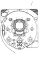
FIG. 1 is a front view of a game board of a pachinko machine P according to the present embodiment. Around the
[0010]
Below the
[0011]
A V
[0012]
In addition, a plurality of
[0013]
FIG. 2 is a block diagram schematically showing the electrical configuration of the pachinko machine P. As shown in FIG. As shown in FIG. 2, the pachinko machine P includes a power
[0014]
On the main control board C, an MPU 11 as a one-chip microcomputer is mounted. The MPU 11 includes a CPU as an arithmetic unit, a ROM that stores a control program, a
[0015]
The MPU 11 has a backup terminal VBB (see FIG. 4), and the backup voltage is supplied from the backup terminal VBB even when the power is turned off. Therefore, even if the power is turned off due to the occurrence of a power failure or the like, the data in the
[0016]
The payout control board H performs payout control of prize balls and rental balls based on signals output from the various switches SW and control commands sent from the main control board C. In addition to the main control board C, A launch control board B for controlling a
[0017]
The
[0018]
Data backed up on the main control board C and the payout control board H can be erased (cleared) by pressing a clear switch SW1 provided on the back side of the pachinko machine P. The backup data is cleared only when the clear switch SW1 is operated at a predetermined timing so that the clearing is not performed by mistake. For example, when the power is turned on while the clear switch SW1 is operated, when the power is turned off while the clear switch SW1 is operated, when the clear switch SW1 is operated a plurality of times within a predetermined time, or Two or more clear switches SW1 are provided, and the backup data is cleared when the clear switches SW1 are operated in a predetermined order or simultaneously.
[0019]
The display control board D is for controlling the fluctuation display of the
[0020]
Between the main control board C and the control boards H, D, S, and L, buffers 8 having fixed inputs and outputs are respectively connected (only one is shown in FIG. 2). Therefore, transmission / reception between the main control board C and each control board H, D, S, L is performed only in one direction from the main control board C to each control board H, D, S, L. , D, S, L cannot be performed on the main control board C.
[0021]
The power
[0022]
Next, with reference to FIG. 3, the supply path of the drive voltage to each part of the pachinko machine P will be described. FIG. 3 is a diagram showing a path through which the drive voltage generated by the
[0023]
The first
[0024]
The output voltage of the 33
[0025]
The power
[0026]
The output voltage of the 12-
[0027]
The second
[0028]
The third
[0029]
The output voltage of the 12
[0030]
The fourth
[0031]
Next, in the pachinko machine P of the present embodiment described above, the operation of supplying drive voltage to various places when a power failure occurs will be described. When a power failure occurs, the power supply from the
[0032]
The 5-
[0033]
Thereafter, with the passage of time, the output voltage of each of the
[0034]
Here, the drive voltages of the main control board C and the payout control board H that are executing the game control end processing are supplied from the first
[0035]
At the shortest, the output voltage of the 5-
[0036]
As described above, the first
[0037]
The second to fourth
[0038]
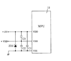
Next, referring to FIG. 4 to FIG. 8, the main control board C and the
[0039]
FIG. 4 is a diagram showing a noise removal circuit connected to the
[0040]
Capacitors C1 and C2 of 0.1 μF are connected between the VDD terminal and the VSS terminal of the
[0041]
When the
[0042]
On the other hand, in the first embodiment, in addition to the capacitors C1 and C2, a capacitor C3 is further connected between the VDD terminal and the VBB terminal of the
[0043]
A modification of the first embodiment shown in FIG. 4 will be described below with reference to FIGS. In addition, the same code | symbol is attached | subjected to the part same as 1st Example, and the description is abbreviate | omitted. Further, the illustration of the 5-
[0044]
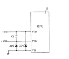
FIG. 5 is a diagram showing a noise removal circuit connected to the
[0045]
FIG. 6 is a diagram showing a noise removal circuit connected to the
[0046]
FIG. 7 is a diagram showing a noise removal circuit connected to the
[0047]
FIG. 8 is a diagram showing a noise removal circuit connected to the
[0048]
FIG. 9 is a diagram showing a noise removal circuit connected to the
[0049]
The present invention has been described based on the embodiments. However, the present invention is not limited to the above-described embodiments, and various improvements and modifications can be easily made without departing from the spirit of the present invention. It can be guessed.
[0050]
For example, in the above embodiment, the noise removal circuit shown in FIGS. 4 to 9 has been described using the main control board C as an example. However, as described above, the noise removal circuit backs up data in addition to the main control board C. The payout control board H is employed. Further, the noise removal circuit is not necessarily limited to that shown in FIGS. 4 to 9, and if the voltage difference between the VDD terminal and the VBB terminal of the MPU at the time of driving falls within a predetermined voltage value, You may make it comprise with another circuit.
[0051]
You may implement this invention in the pachinko machine etc. of a different type from the said Example. For example, once a big hit, a pachinko machine that raises the expected value of the big hit until a big hit state occurs (for example, two times or three times) including that (for example, a two-time right item, a three-time right item) May also be implemented. Moreover, after the jackpot symbol is displayed, it may be implemented as a pachinko machine that enters a special game state under the condition that a ball is awarded in a predetermined area. Further, in addition to the pachinko machine, the game machine may be implemented as various game machines such as an alepatchi, a sparrow ball, a slot machine, a game machine in which a so-called pachinko machine and a slot machine are integrated.
[0052]
In the slot machine, for example, a symbol is changed by operating a control lever in a state where a symbol effective line is determined by inserting coins, and a symbol is stopped and confirmed by operating a stop button. Is. Therefore, the basic concept of the slot machine is that it is provided with variable display means for confirming and displaying the identification information after variably displaying the identification information string composed of a plurality of identification information, and resulting from the operation of the starting operation means (for example, the operation lever) Then, the change of the identification information is started, and the change of the identification information is stopped due to the operation of the operation means for stop (for example, the stop button) or after the lapse of a predetermined time, and the fixed identification information at the time of the stop Is a slot machine provided with special game state generating means for generating a special game state advantageous to the player on the condition that the specific identification information is a necessary condition. In this case, coins, medals, etc. are representative examples of game media As mentioned.
[0053]
In addition, as a specific example of a gaming machine in which a pachinko machine and a slot machine are integrated, a variable display means for displaying a symbol after a symbol string composed of a plurality of symbols is displayed, and a handle for launching a ball is provided. What is not provided. In this case, after throwing a predetermined amount of spheres based on a predetermined operation (button operation), for example, the change of the symbol is started due to the operation of the operation lever, for example, due to the operation of the stop button, or With the passage of time, the fluctuation of the symbol is stopped, and a jackpot state advantageous to the player is generated on the condition that the confirmed symbol at the time of stoppage is a so-called jackpot symbol. A lot of balls are paid out.
[0054]
The modification of this invention is shown below. 2. The gaming machine according to
[0055]
2. The gaming machine or gaming machine according to
[0056]
2. The gaming machine or the
[0057]
2. The gaming machine according to
[0058]
2. The gaming machine or the
[0059]
2. A gaming machine or a gaming machine according to
[0060]
2. The gaming machine according to
[0061]
The gaming machine according to
[0062]
The gaming machine 9 according to
[0063]
The
[0064]
The gaming machine according to
[0065]
【The invention's effect】
According to the gaming machine of the present invention, when the supply of the drive voltage is interrupted, the storage unit holds the stored content (backups the data) with the backup voltage supplied from the power supply unit. Various noises are added to the storage means. Since such noises are removed or suppressed by the noise removing means, there is an effect that the gaming machine can be operated normally .
[Brief description of the drawings]
FIG. 1 is a front view of a game board of a pachinko machine that is one embodiment of the present invention.
FIG. 2 is a block diagram schematically showing an electrical configuration of the pachinko machine.
FIG. 3 is a diagram showing a supply path of a drive voltage generated by a power supply circuit to each control board and the like.
FIG. 4 is a diagram showing a noise removal circuit of a first embodiment provided in an MPU of a main control board.
FIG. 5 is a diagram showing a noise removal circuit of a second embodiment provided in the MPU of the main control board.
FIG. 6 is a diagram showing a noise removal circuit of a third embodiment provided in the MPU of the main control board.
FIG. 7 is a diagram showing a noise removal circuit of a fourth embodiment provided in the MPU of the main control board.
FIG. 8 is a diagram showing a noise removal circuit of a fifth embodiment provided in the MPU of the main control board.
FIG. 9 is a diagram showing a noise removal circuit of a sixth embodiment provided in the MPU of the main control board.
[Explanation of symbols]
30
12, 13 RAM (storage means)
C1 capacitor (noise removal hand stage)
C2 capacitor (noise removal hand stage)
C3 and C4 capacitors (noise removal means)
ZD1 to ZD3 constant voltage diode (noise removal means)
ZD4 Zener diode (noise removal hand stage)
ZD5 Zener diode (noise removal hand stage)
C Main control board H Discharge control board P Pachinko machine (game machine)
Claims (1)
その電源手段から駆動電圧の供給をうけて動作すると共に、その駆動電圧の供給が途絶えても前記バックアップ電圧が供給されることにより記憶内容を保持する記憶手段と、
前記駆動電圧の供給ラインと前記バックアップ電圧の供給ラインとの電圧差を比較する比較手段と、
その比較手段による比較の結果、前記電圧差が所定値以上である場合に、前記記憶手段へのアクセスを禁止する禁止手段と、
前記電源手段から前記記憶手段へ駆動電圧が供給されている間、前記駆動電圧と前記バックアップ電圧との電圧差を前記所定値より小さく維持することにより、前記記憶手段へ加わるノイズを除去又は抑制するノイズ除去手段とを備えていることを特徴とする遊技機。Power supply means for supplying drive voltage and backup voltage;
A storage unit that operates by receiving a supply of drive voltage from the power supply unit, and holds the storage content by supplying the backup voltage even when the supply of the drive voltage is interrupted;
A comparing means for comparing a voltage difference between the drive voltage supply line and the backup voltage supply line;
As a result of comparison by the comparison means, when the voltage difference is greater than or equal to a predetermined value, prohibiting means for prohibiting access to the storage means;
While the drive voltage is supplied from the power supply means to the storage means, the voltage difference between the drive voltage and the backup voltage is kept smaller than the predetermined value, thereby removing or suppressing noise applied to the storage means. A gaming machine comprising noise removing means.
Priority Applications (1)
| Application Number | Priority Date | Filing Date | Title |
|---|---|---|---|
| JP2000140779A JP4724898B2 (en) | 2000-05-12 | 2000-05-12 | Game machine |
Applications Claiming Priority (1)
| Application Number | Priority Date | Filing Date | Title |
|---|---|---|---|
| JP2000140779A JP4724898B2 (en) | 2000-05-12 | 2000-05-12 | Game machine |
Related Child Applications (1)
| Application Number | Title | Priority Date | Filing Date |
|---|---|---|---|
| JP2010173797A Division JP5182335B2 (en) | 2010-08-02 | 2010-08-02 | Game machine |
Publications (3)
| Publication Number | Publication Date |
|---|---|
| JP2001321542A JP2001321542A (en) | 2001-11-20 |
| JP2001321542A5 JP2001321542A5 (en) | 2007-06-28 |
| JP4724898B2 true JP4724898B2 (en) | 2011-07-13 |
Family
ID=18648014
Family Applications (1)
| Application Number | Title | Priority Date | Filing Date |
|---|---|---|---|
| JP2000140779A Expired - Lifetime JP4724898B2 (en) | 2000-05-12 | 2000-05-12 | Game machine |
Country Status (1)
| Country | Link |
|---|---|
| JP (1) | JP4724898B2 (en) |
Cited By (1)
| Publication number | Priority date | Publication date | Assignee | Title |
|---|---|---|---|---|
| JP2017063862A (en) * | 2015-09-28 | 2017-04-06 | 株式会社ニューギン | Game machine |
Families Citing this family (4)
| Publication number | Priority date | Publication date | Assignee | Title |
|---|---|---|---|---|
| JP4858485B2 (en) * | 2008-05-08 | 2012-01-18 | 株式会社三洋物産 | Game machine |
| JP2011115269A (en) * | 2009-12-01 | 2011-06-16 | Toyomaru Industry Co Ltd | Game machine |
| JP2011152455A (en) * | 2011-05-16 | 2011-08-11 | Sanyo Product Co Ltd | Game machine |
| JP5720645B2 (en) * | 2012-08-31 | 2015-05-20 | 株式会社三洋物産 | Game machine |
Family Cites Families (7)
| Publication number | Priority date | Publication date | Assignee | Title |
|---|---|---|---|---|
| JPS5849396A (en) * | 1981-09-07 | 1983-03-23 | Toyo Jozo Co Ltd | 4"-deoxy-14-membered ring macrolide antibiotic substance |
| JPH0749728A (en) * | 1993-08-06 | 1995-02-21 | Sanyo Electric Co Ltd | Backup power supply circuit for microcomputer |
| JPH08229192A (en) * | 1995-02-28 | 1996-09-10 | Sankyo Kk | Gaming apparatus |
| JP2715273B2 (en) * | 1995-06-13 | 1998-02-18 | 株式会社大一商会 | Pachinko machine |
| JP4156149B2 (en) * | 1999-10-29 | 2008-09-24 | 株式会社三共 | Game machine |
| JP4219078B2 (en) * | 2000-04-11 | 2009-02-04 | 株式会社三共 | Game machine |
| JP4356957B2 (en) * | 2000-04-12 | 2009-11-04 | 株式会社ソフィア | Game machine |
-
2000
- 2000-05-12 JP JP2000140779A patent/JP4724898B2/en not_active Expired - Lifetime
Cited By (1)
| Publication number | Priority date | Publication date | Assignee | Title |
|---|---|---|---|---|
| JP2017063862A (en) * | 2015-09-28 | 2017-04-06 | 株式会社ニューギン | Game machine |
Also Published As
| Publication number | Publication date |
|---|---|
| JP2001321542A (en) | 2001-11-20 |
Similar Documents
| Publication | Publication Date | Title |
|---|---|---|
| JP5120410B2 (en) | Game machine | |
| JP2009000241A (en) | Game machine | |
| JP4724898B2 (en) | Game machine | |
| JP4724897B2 (en) | Game machine | |
| JP3856613B2 (en) | Game machine | |
| JP4321642B2 (en) | Game machine | |
| JP2004016791A (en) | Game machine | |
| JP2003275429A (en) | Pachinko game machine | |
| JP4608734B2 (en) | Game machine | |
| JP2001321542A5 (en) | ||
| JP5182335B2 (en) | Game machine | |
| JP5720645B2 (en) | Game machine | |
| JP2001321532A5 (en) | ||
| JP4023322B2 (en) | Game machine | |
| JP4438273B2 (en) | Game machine | |
| JP5979287B2 (en) | Game machine | |
| JP5880600B2 (en) | Game machine | |
| JP5700002B2 (en) | Game machine | |
| JP5994831B2 (en) | Game machine | |
| JP2001321496A5 (en) | ||
| JP5895991B2 (en) | Game machine | |
| JP2004016815A (en) | Game machine | |
| JP6090483B2 (en) | Game machine | |
| JP6061042B2 (en) | Game machine | |
| JP4576663B2 (en) | Game machine |
Legal Events
| Date | Code | Title | Description |
|---|---|---|---|
| RD02 | Notification of acceptance of power of attorney |
Free format text: JAPANESE INTERMEDIATE CODE: A7422 Effective date: 20070221 |
|
| A521 | Written amendment |
Free format text: JAPANESE INTERMEDIATE CODE: A523 Effective date: 20070511 |
|
| A621 | Written request for application examination |
Free format text: JAPANESE INTERMEDIATE CODE: A621 Effective date: 20070511 |
|
| A977 | Report on retrieval |
Free format text: JAPANESE INTERMEDIATE CODE: A971007 Effective date: 20100210 |
|
| A131 | Notification of reasons for refusal |
Free format text: JAPANESE INTERMEDIATE CODE: A131 Effective date: 20100601 |
|
| A521 | Written amendment |
Free format text: JAPANESE INTERMEDIATE CODE: A523 Effective date: 20100802 |
|
| TRDD | Decision of grant or rejection written | ||
| A01 | Written decision to grant a patent or to grant a registration (utility model) |
Free format text: JAPANESE INTERMEDIATE CODE: A01 Effective date: 20110315 |
|
| A61 | First payment of annual fees (during grant procedure) |
Free format text: JAPANESE INTERMEDIATE CODE: A61 Effective date: 20110328 |
|
| R150 | Certificate of patent or registration of utility model |
Ref document number: 4724898 Country of ref document: JP Free format text: JAPANESE INTERMEDIATE CODE: R150 Free format text: JAPANESE INTERMEDIATE CODE: R150 |
|
| FPAY | Renewal fee payment (event date is renewal date of database) |
Free format text: PAYMENT UNTIL: 20140422 Year of fee payment: 3 |
|
| R250 | Receipt of annual fees |
Free format text: JAPANESE INTERMEDIATE CODE: R250 |
|
| R250 | Receipt of annual fees |
Free format text: JAPANESE INTERMEDIATE CODE: R250 |
|
| R250 | Receipt of annual fees |
Free format text: JAPANESE INTERMEDIATE CODE: R250 |
|
| R250 | Receipt of annual fees |
Free format text: JAPANESE INTERMEDIATE CODE: R250 |
|
| R250 | Receipt of annual fees |
Free format text: JAPANESE INTERMEDIATE CODE: R250 |
|
| R250 | Receipt of annual fees |
Free format text: JAPANESE INTERMEDIATE CODE: R250 |