JP4707322B2 - Capacity loaded probe and inspection jig using the same - Google Patents
Capacity loaded probe and inspection jig using the same Download PDFInfo
- Publication number
- JP4707322B2 JP4707322B2 JP2003566566A JP2003566566A JP4707322B2 JP 4707322 B2 JP4707322 B2 JP 4707322B2 JP 2003566566 A JP2003566566 A JP 2003566566A JP 2003566566 A JP2003566566 A JP 2003566566A JP 4707322 B2 JP4707322 B2 JP 4707322B2
- Authority
- JP
- Japan
- Prior art keywords
- probe
- metal
- metal pipe
- power supply
- movable pin
- Prior art date
- Legal status (The legal status is an assumption and is not a legal conclusion. Google has not performed a legal analysis and makes no representation as to the accuracy of the status listed.)
- Expired - Fee Related
Links
Images


Classifications
-
- G—PHYSICS
- G01—MEASURING; TESTING
- G01R—MEASURING ELECTRIC VARIABLES; MEASURING MAGNETIC VARIABLES
- G01R1/00—Details of instruments or arrangements of the types included in groups G01R5/00 - G01R13/00 and G01R31/00
- G01R1/02—General constructional details
- G01R1/06—Measuring leads; Measuring probes
- G01R1/067—Measuring probes
- G01R1/06772—High frequency probes
-
- G—PHYSICS
- G01—MEASURING; TESTING
- G01R—MEASURING ELECTRIC VARIABLES; MEASURING MAGNETIC VARIABLES
- G01R1/00—Details of instruments or arrangements of the types included in groups G01R5/00 - G01R13/00 and G01R31/00
- G01R1/02—General constructional details
- G01R1/06—Measuring leads; Measuring probes
- G01R1/067—Measuring probes
- G01R1/06711—Probe needles; Cantilever beams; "Bump" contacts; Replaceable probe pins
- G01R1/06716—Elastic
- G01R1/06722—Spring-loaded
Description
【0001】
【発明の属する技術分野】
本発明は、たとえば携帯電話機に組み込まれる増幅回路やミキサ回路など、高周波・高速用(アナログで周波数の高いものを高周波といい、デジタルでパルス幅およびパルス間隔が非常に小さいものを高速という、以下同じ)の半導体ウェハ、IC、またはモジュールなどを検査する高周波・高速用デバイスを検査する場合などに、その被検査デバイスと検査装置との接続を確実にしながら、外来ノイズの影響を極力小さくすることができる容量装荷型プローブおよびそれを用いた検査治具に関する。
【0002】
【従来の技術】
たとえば、半導体ウェハ、ICあるいはモジュールなどの高周波や高速のデバイスを検査する場合、リードなどが露出しているとその部分でノイズを拾いやすいため、たとえば特開2001−99889号公報にも開示され、図12(a)に示されるように、金属ブロック1内に設けられるスプリング入りのRF信号用(高周波および高速の両方を含む意味で使用)プローブ3、電源用プローブ4および接地用プローブ5を有する検査治具を介して被検査デバイス20の各電極端子21〜23と接続されるように構成されている。このような検査治具で、RF信号は同軸ケーブル7を介して、RF信号用プローブ3に接続され、スプリングの縮みにより被検査デバイス20と金属ブロック1上の薄い押え板8との間に間隙が生じないようにすると共に、スプリングによりRF信号用プローブ3と被検査デバイス20の電極端子との接触を確実にして信号を入出力させることにより、できるだけノイズを拾わないような構成になっている。なお、図12(a)において、6はプリント基板などからなり、入力側の電源配線を形成する配線基板を示している。
【0003】
このような構造にしても、高周波または高速用では、ノイズを拾いやすく、金属ブロック1内のスプリング入りプローブの部分でノイズを拾うことがあり、前述の特開2001−99889号公報では、RF信号用プローブ3を同軸構造にすることを開示し、ノイズを拾う余地のない構造が考えられている。一方、電源端子23に高周波や高速のノイズが乗っても、電源電圧がそのノイズにより振られることになり、増幅器などは発振したりして正確な測定をすることができない。そのため、電源用プローブ4の入力側の配線基板(プリント基板)6に、たとえば図12(b)に示されるようなコイルLとキャパシタCのLC回路からなるローパスフィルタ61を形成したり、電源用プローブ4の入力側と配線基板(プリント基板)6上のアースとの間にチップコンデンサ(バイパスコンデンサ)を接続することにより、電源配線に乗った高周波・高速のノイズを除去する方法が用いられている。
【0004】
一方、入力信号端子には、RF信号に限らず、端子によって、DCレベルに近い信号から100MHzにおよぶ種々の中低周波の信号が入力されて検査がなされる。これらの中低周波の信号端子に対してRFノイズが入力されても、正確な検査をすることができない。これらの中低周波入力信号用プローブを同軸構造に形成しても、デバイス側または検査装置側で混入したRFノイズは、そのまま被検査デバイスの端子に入力されてしまうことになるため、前述のように、正確な検査をすることができなくなる。
【0005】
【発明が解決しようとする課題】
前述のように、高周波用や高速用のデバイスを検査する検査治具では、そのデバイスに接続される配線などにより拾うノイズの影響を受け難くするため、被検査デバイスとの接続部を、スプリングを介して伸縮する可動ピンを有するコンタクトプローブを金属ブロック内に設けて接触させる構造とされている。これにより、被検査デバイスと金属ブロックとの間隙をなくして確実に接続することができ、ノイズを拾い難くなる。さらには、RF信号用プローブは、前述のように、金属ブロック内においても同軸構造にすることが試みられている。一方で、近年の高周波および高速化の進展と共に、回路の高集積化およびパッケージの小型化は目覚しいものがあり、端子数(電極数)の増加および端子間ピッチの縮小化により、金属ブロックを使用していない構造では影響を受けやすいのは当然としても、金属ブロック内の電源プローブであっても非常にノイズが重畳されやすい状況になり、金属ブロック内の電源プローブへの入力側にローパスフィルタやチップコンデンサを設ける構造では、完全には、ノイズの影響を受けない正確な検査をすることができないという問題がある。
【0006】
さらに、近年の高周波・高速用デバイスの進化により、入力信号の変化により出力がローからハイになったり、ハイからローになったりする過渡期にデバイスの演算エラーや強制リセットを引き起こすなど検査に異常が出やすいことを見出し、本発明者らはその原因を鋭意検討を重ねて調べた結果、出力電圧が変化する過渡時間が早くなり、それに伴い、その電圧変化によって発生する電源電流の瞬時的変化が電源端子の電圧降下を引き起こすことに基づいていることを見出した。すなわち、電源電流がステップ状に増加すると、前述の図12(a)に示されるような構造で、長さが4mm程度の電源用プローブ4では、プローブが細いため2nH程度のインダクタンスL1を有しており、また、プローブ周辺の浮遊容量として、C2=0.5pFを想定すると、図11(a)に示されるような等価回路になる(図11(a)で、C2は、キャパシタが接続されている訳ではないが、浮遊容量を等価回路で示している)。その結果、たとえば図11(b)に示されるように、電流I1がA1=10mAから、A2=50mAにステップ状(立上り時間0の理想的状態)に変化すると、電圧は、図11(c)に示されるように、3Vから1.7V程度まで低下しており、それが原因で検査データに支障が生じることを見出した。
【0007】
本発明は、このような問題を解決するためになされたもので、高周波・高速化と共に高集積化、パッケージの小型化による電極プローブ間ピッチの縮小化が図られるデバイスを検査する場合でも、電源端子への接続に細いプローブを用いながら、インダクタンスによる電源端子での電圧降下の影響を殆ど受けることのない容量装荷型プローブを提供することを目的とする。
【0008】
本発明の他の目的は、高周波・高速化と共に高集積化されるデバイスでも、その端子に入力される信号に応じてノイズを低減させることにより、ノイズの影響を受けることなく正確な検査をすることができる容量装荷型プローブおよびそれを用いた高周波・高速用デバイスなどの検査装置用の検査治具を提供することにある。
【0009】
【課題を解決するための手段】
本発明による容量装荷型プローブは、金属パイプと、該金属パイプ内に該金属パイプと電気的に接続して設けられ、少なくとも前記金属パイプの一端部から突出する突出長を可変とし得る可動ピンと、外周面および内周面に第1の金属膜および第2の金属膜がそれぞれ空隙部を形成することなく密着して設けられる誘電体筒とを有し、該誘電体筒が前記金属パイプの外周に設けられることにより該金属パイプと前記第2の金属膜とが電気的に接続される電源用の容量装荷型プローブであって、前記誘電体筒は比誘電率が38以上の材料からなり、前記可動ピンと前記第1の金属膜との間に50pF以上の容量が形成されている。
【0010】
ここに可動ピンとは、たとえばリード線がスプリングなどにより保持されて押し付ければスプリングなどによりその先端が縮むような、先端が軸方向に沿って移動し得るピンを意味する。
【0011】
このようなコンタクトプローブの外周面にキャパシタが形成されていることにより、電源端子や信号端子に接続するプローブとして使用する場合に、電源端子での電圧の降下を防止したり、ノイズを除去することができる。すなわち、被検査デバイスが、RF(アナログの周波数が高い高周波やデジタルのショートパルスでパルス間隔が小さい高速の両方を含む意味であり、アナログまたはパルスの繰返しが1GHz程度以上のものを意味する、以下同じ)用であると、電源用プローブのインダクタンスにより、たとえば出力がローからハイなどの電流の切替り時に電圧降下が生じるが、このキャパシタによりその電圧降下を支障がない程度に小さくすることができる。これは、キャパシタが付加されることにより、インダクタとキャパシタとの充放電による補償がなされることに基づいている。
【0012】
さらに、電源端子や、入力信号でDCレベルに近い信号もしくはサイン波やパルスの繰返しの小さい中低周波信号の信号端子に接続する場合に、電源用プローブや信号用プローブにキャパシタが形成されていることにより、電源ラインや信号ラインに混入したRFノイズをキャパシタにより確実に落すことができ、ノイズの影響を受けないで、信頼性の高い検査をすることができる。
【0013】
本発明による容量装荷型プローブの他の形態は、金属パイプと、該金属パイプ内に該金属パイプと電気的に接続して設けられ、少なくとも前記金属パイプの一端部から突出する突出長を可変とし得る可動ピンと、前記金属パイプの外周面に空隙部を形成することなく密着して設けられる誘電体層と、該誘電体層の外周面に空隙部を形成することなく密着して設けられる第1の金属膜とからなり、前記誘電体層は比誘電率が38以上の材料からなり、前記可動ピンと前記第1の金属膜との間に50pF以上の容量が形成される構造でもよい。なお、誘電体筒の内壁および外壁に設けられる金属膜は、たとえば無電解メッキなどにより形成される。また、薄膜で誘電体層を形成するには、たとえば金属パイプを回転させながらスパッタリングや真空蒸着などによっても形成することができるし、誘電体材料を有機溶媒などに溶解した液を金属パイプの外周に塗布して乾燥、焼成させるゾルゲル法によっても形成することができる。
【0014】
本発明による検査治具は、金属ブロックと、先端部の突出長が可動する可動ピンを有し、前記金属ブロックの一面側に前記可動ピンの先端部が突出するように、該金属ブロックを貫通して設けられる電源用および信号用の複数のプローブとを具備し、前記金属ブロックの前記一面側に被検査デバイスが押し付けられ、該被検査デバイスの各電極端子と前記プローブの先端部とを接触させて前記被検査デバイスの特性検査をする検査治具であって、前記複数のプローブのうちの少なくとも一部の電源端子に接続される電源用プローブは、請求項1〜4のいずれか1項に記載の容量装荷型プローブからなっている。
【0015】
この構造にすることにより、電源用プローブや信号用プローブの少なくとも一部の周囲にRFノイズをバイパスするキャパシタが形成されているため、被検査デバイスの電源端子や信号端子の直前で、RFノイズをバイパスさせることができ、電源用や信号用のプローブにノイズが乗るどころか、配線基板(プリント基板)側で完全に除去しきれなかったRFノイズが残っていても、バイパス用キャパシタを介して完全に除去される。その結果、可動ピンを介してデバイスに接続される電源用や中低周波の信号用のプローブからのノイズの侵入は完全になくなり、ノイズの影響を受けない正確な検査をすることができる。さらに、電源用プローブに容量装荷型プローブが用いられることにより、デバイス内部の電流変化によって発生する電源端子における電圧の降下を抑えることができ、一般的な電源電圧許容範囲の10%以内に抑えることができる。
【0016】
本明細書において、正弦波またはパルスの繰返しとは、アナログ信号の場合にはその周波数を、デジタル信号の場合には、そのハイ、ローの繰返し早さを意味する。
【0017】
前記被検査デバイスの電源端子に接続される電源用プローブに、容量が50pF以上、さらに好ましくは100pF以上のキャパシタが接続された容量装荷型プローブが用いられることにより、入力信号の変化に対しても電源電圧が10%以上降下することは殆どなく、また、400MHz以上(100pF以上であれば、200MHz以上)の高周波ノイズを10dB以上減衰させることができ、高いRFノイズはさらに大きく減衰させることができ、殆ど完全にノイズを除去することができるため好ましい。
【0018】
【発明の実施の形態】
つぎに、図面を参照しながら本発明の容量装荷型プローブおよびそれを用いた検査治具について説明をする。本発明による検査治具は、被検査デバイス20と図示しない検査装置とを接続するもので、図1(a)および1(b)にその平面および一部断面の側面説明図が示されるように、先端部の突出長が可動する可動ピン11を有し、金属ブロック1の一面側に可動ピン11の先端部が突出するように、信号用プローブ3、電源用プローブ4および接地用プローブ5など複数のプローブが、金属ブロック1を貫通して設けられている。そして、この金属ブロック1の一面側に被検査デバイス20が押し付けられ、その被検査デバイス20の各電極端子21〜24とそれぞれプローブ3〜5の先端部とを接触させて被検査デバイス20の特性検査がなされる。本発明では、この複数のプローブのうちの少なくとも一部のプローブは、そのプローブの外周に誘電体層と金属膜が設けられることによりキャパシタが形成された容量装荷型プローブからなっている。
【0019】
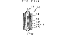
この容量装荷型プローブ10は、図2(a)にその一実施形態の断面説明図が示されるように、金属パイプ13内に、その金属パイプ13の少なくとも一端部から突出する先端部の突出長を可変とし得るように、可動ピン11、12がその金属パイプ13と電気的に接続して設けられ、その金属パイプ13の外周に誘電体層15が設けられ、誘電体層15の外周面に第1の金属膜17が設けられることにより、可動ピン11と第1の金属膜17との間にキャパシタンスが形成されている。
【0020】
このキャパシタ18を形成するための誘電体層として、図2に示される例では、誘電体を筒状に形成した誘電体筒15が用いられている。そして、誘電体筒15の内周壁および外周壁に第2および第1の金属膜16、17が無電解メッキなどにより設けられることにより、キャパシタ18が形成されている。この誘電体筒15の両面に第1および第2の金属膜17、16が設けられることにより、誘電体の両面に空隙が生じなくなり、キャパシタンスの機能を充分に奏するようになっている。第2の金属膜16は、金属パイプ13と電気的に接続されている。
【0021】
誘電体筒15は、図2(b)にその斜視説明図が示されるように、たとえば内径D1が0.3mm程度、外径D2が0.6mm程度、長さLが6mm程度の大きさに形成される。これは、前述のように、ICなどの高集積化に伴い、電極端子数が増大し、最近では、チップの周囲のみに電極端子を設けるのではなく、BGA(ball grid array)パッケージによりチップ全面に形成されるようになり、しかも電極端子数が多い場合には、1cm2当り400個程度の電極端子数が設けられるため、プローブの間隔も非常に小さくなるからである。これらの電極端子数のうち、電源端子が1/4程度、接地端子が1/4程度、残りがRF信号など、信号の入出力端子とされている。
【0022】
このキャパシタ18の効果を調べるため、本発明者らは、この構造のプローブ外周面にキャパシタを形成した容量装荷型プローブを接続した場合の周波数に対する挿入損失、すなわちノイズ除去程度をシミュレーションにより調べた。その結果を図3に示す。図3は、図2(a)に示されるキャパシタの容量を種々変えたときの周波数に対する挿入損失を縦軸(下向き)に示したもので、キャパシタの容量を10pF、50pF、100pF、530pF、および1060pFとした場合をそれぞれ示している。なお、キャパシタなしは、容量装荷型プローブではない従来のプローブの周波数特性を示している。
【0023】
一般に、10dB程度の挿入損失があれば、ノイズ除去に大きな効果があり、20dB程度の挿入損失があれば、ノイズの影響を殆ど完全に除去することができることから、図3から明らかなように、1060pFあれば、25MHz程度以上の周波数のノイズを除去することができ、50MHz以上であれば、殆ど完全に除去することができる。また、1GHz以上のRFノイズに対しては、100pFあれば、完全にノイズの影響をなくすることができ、50pF以上あれば、充分にノイズを減衰させることができることが分る。これに対して、従来のキャパシタなし(浮遊容量は0.5pF程度あると考えられる)のプローブでは、20GHzまでの挿入損失は、2dB以下であり、殆どRFノイズの除去効果がないことが分る。
【0024】
一方、たとえば容量が50pFであれば、数十MHz帯では殆ど減衰せず、1GHz以上では大幅な減衰が見られ、たとえば信号を入力する信号用プローブで、入力信号の周波数が数十MHz以下の信号であれば、50pF程度の容量を有するキャパシタが装荷されたプローブを用いることにより、RFノイズを除去した信号を入力して信頼性のある検査をすることができることを、本発明者らは見出した。すなわち、信号用プローブには、その入力信号の周波数に応じて、同軸構造のプローブにするよりも、信号は減衰しないで、それより高い周波数のノイズのみを減衰させる大きさの容量のキャパシタを装荷したプローブを用いる方が好ましいことを、本発明者らは見出した。
【0025】
このような容量を変化させるには、誘電体層15の材料を変えて、比誘電率の異なるものを使用したり、誘電体層15の厚さまたはプローブの長さを変えることにより、容量を変化させることができる。たとえば、セラミックスとしてよく用いられているチタン酸バリウム(比誘電率2200)と高誘電率セラミックスと称されている比誘電率が38程度のセラミックスを用いれば、図2(a)および2(b)に示される構造で、表1に示されるような寸法のプローブを形成することにより、上記容量のプローブを形成することができる。しかし、さらに誘電体の材質や厚さを変えることにより、容量を自由に調整することができる。とくに、後述するように誘電体を薄膜により形成することにより、その厚さを非常に薄くすることができ、容量を大きくすることができる。
【0026】
【表1】

実際に、表1に示される530pFのキャパシタの寸法で容量装荷型プローブを形成して、周波数に対する挿入損失を測定した。その結果が図4に示されている。なお、表1に示される寸法で形成した結果、実際の容量は470pFであった。図4から、図3と同様に、50MHzで既に15dB程度挿入損失が得られ、200MHz以上ではほぼ20dB以上の挿入損失が得られ、ノイズを殆ど完全に除去できることを示している。なお、図4で、指示1は1GHz、27.595dBを、指示2は5GHz、33.877dBを、指示3は10GHz、27.661dBを、指示4は15GHz、34.276dBを、指示5は20GHz、39.060dBをそれぞれ示している。
【0028】
このように、500pF程度あれば、充分低い周波数から高い周波数まで大きな挿入損失を得られるため、電源用プローブやDCレベルに近い繰返しの小さい(低い周波数)入力信号に対しては、充分である。しかし、前述の図3に示されるように、100pFあれば、200MHz以上で、十分の挿入損失があり、電源用プローブとして実用的である。
【0029】
一方、前述のように、本発明者らは、電源用プローブのインダクタンス成分により、信号変化により出力の過渡時間に、電源端子における電圧の降下が生じて、正確な検査を行えない場合があることを見出した。そして、この電源用プローブに容量装荷型プローブを用いることにより、電圧降下を問題とならない10%以下に抑えることができた。この容量装荷型プローブを電源用プローブに用いた場合に、電源端子における電圧降下を防止することができる効果について説明をする。
【0030】
容量装荷型プローブを電源用プローブとして用いた場合、被検査デバイスとの接続部の等価回路は図5に示されるようになる。この電源電圧V1を3Vdc(直流)とし、R1=0.1Ω、L1=2nHとし、C1を1000pFと100pFとした場合に、前述の図11(b)に示されるように、電流を10mAから、50mAにステップ状(立上り時間0の理想的状態)に変化させたときの電源端子における電圧V2をシミュレーションにより調べた。その結果を図6(a)および図6(b)にそれぞれ示す。なお、図6(c)は、キャパシタが装荷されない(0.5pFの浮遊容量を想定している)従来のプローブを用いたときの電圧降下を示す図で、図11(c)に示したものを、図6(a)および6(b)と同じスケールで示したもので、シミュレーションの条件は同じである。
【0031】
図6(a)〜6(c)から明らかなように、キャパシタなし(浮遊容量0.5pFを想定)の従来のプローブを用いた場合には、1.32V(44%)という大幅な電圧降下が現れるのに対して、1000pFの容量のキャパシタが装荷されることにより、電圧が安定するまでの時間は長くなるものの、電圧の変化量は0.06V程度で、2%程度と非常に変化量を小さくすることができる。なお、長時間電圧が脈動しても、その変化量が小さいため、何ら影響を受けない。また、100pFのキャパシタを装荷した場合でも、図6(b)に示されるように、電源端子における電圧の変動は1000pFの場合に比べれば大きくなるが、それでも0.18V程度で、6%程度と小さく、一般に変動の限度とされる10%を充分にクリアすることができる。すなわち、電源用プローブに100pF以上の容量を装荷したプローブを用いることにより、非常に急激な電流の変化に対しても、電圧変動を支障がない程度に抑えることができる。
【0032】
このように、容量装荷型プローブを電源用プローブとして用いることにより、電源端子における電圧の変動を防止することができるのは、たとえば一つの見方として、電源用プローブの有するインダクタンスと、装荷された容量との充放電の作用により電圧が補償されるためと考えられる。その結果、信号により被検査デバイスの出力が瞬時的にローからハイ、あるいはハイからローに変化しても、電源端子における電圧の変動を抑制することができるため、被検査デバイスの演算エラーや強制リセットを引き起こす可能性を皆無にすることができ、非常に安定した検査をすることができる。なお、高周波・高速用デバイスでは、配線による引き回しをできるだけ少なくするため、前述のように、1個のデバイスに対しても、電源端子は非常に沢山形成される。そのため、1個の電源用プローブでこの大きさの容量が確保されなくても、並列となる沢山の電源プローブにより、装荷される容量を大きくすることができる。また、逆に全ての電源用プローブに容量装荷型プローブを用いなくても、電源用プローブによる電圧の降下抑制およびノイズ除去の効果を奏することができる。
【0033】
前述のように、このような容量装荷型プローブ10を電源用プローブ4として用い、電源ライン上のノイズを落としたり、電源電圧の変動を防止するためには、容量が大きいほど低い周波数のノイズでも挿入損失が大きくて減衰させることができ、さらに高い周波数での挿入損失はより大きくなると共に、電源端子における電圧の変動を小さくすることができるため好ましい。しかし、前述のように、ノイズ除去および電圧変動のいずれの目的にも、100pF以上の容量があれば全く問題はないが、50pF程度以上あれば充分である。なお、プローブ自身は、前述のように、高集積化に伴い太さを余り大きくすることはできず、むしろ細くすることが要求され、キャパシタの面積を余り増やすことはできない。そのため、誘電体層15として、比誘電率ができるだけ大きい誘電体を用いることが好ましい。
【0034】
一方、信号用プローブでは、種々の信号ラインがあり、DCレベルに近いものから、1GHz以上のRF信号まで種々あり、100MHz程度以下の中低周波信号ラインにも1GHz以上のRFノイズが重畳される場合があり、選択的にこれらのノイズを除去することが望まれる。そのため、印加される信号の周波数に応じて、信号端子ごとに容量を選定した容量装荷型プローブを用いることにより、確実にノイズを除去することができて、信頼性の高い検査をすることができる。
【0035】
このような容量装荷型キャパシタに用いる誘電体としては、たとえば前述の誘電体筒を用いる場合には、チタン酸バリウム(比誘電率700〜20000程度)、チタン酸ストロンチウム(比誘電率1500〜4000程度)のような比誘電率の大きいものの他に、高誘電率セラミックス(比誘電率10〜50程度)や、アルミナ(比誘電率9〜10)のような焼成したセラミックス類を用いることができる。チタン酸バリウムやチタン酸ストロンチウムなど比誘電率の大きい材料により形成されることにより、内外径がそれぞれ0.3mm、0.6mmで長さが6mm程度の非常に小さな電源用プローブでも、高周波ノイズを殆ど完全にバイパスさせる1000pF程度以上の大きな容量を形成することができ、低い周波数のノイズでも容易に除去することができるため好ましい。
【0036】
また、後述するように、誘電体筒を用いないで、たとえば金属パイプ13の外表面に直接薄膜を成膜することもできる。このような成膜材料としては、前述の材料の他にも、チタン酸鉛、チタン酸ジルコン酸鉛(PZT;比誘電率700〜1000程度)、チタン酸ジルコン酸ランタン鉛(PLZT)、チタン酸バリウムストロンチウム(BST;比誘電率1000〜3000程度)、タンタル酸ビスマスストロンチウム(SBT)、ビスマスチタネート(BIT;比誘電率150〜220)などのビスマス系化合物などを用いることができる。これらの材料は比誘電率も大きく、5〜20μm程度の薄膜で形成し得るため、より容量の大きいキャパシタを形成しやすい。
【0037】
前述の誘電体筒タイプで形成する場合、キャパシタは、電流が流れないため、電極の導電率はあまり問題にならないが、誘電体と電極用金属とが密着していないと誘電率の小さい空隙部が形成され、容量を下げることになるため、誘電体筒15の内周面および外周面には金属膜が密着して設けられることが好ましい。そのため、誘電体筒15の内部にも無電解メッキなどによりNiなどをメッキをし、さらに必要によりその上に銀や金などをメッキすることにより第2の導電膜16が設けられ、外周面にも同様に無電解メッキなどにより第1の導電膜17が形成されている。内周面は、直径が0.3mm程度と非常に小さいため、メッキ液が浸透しにくいが、たとえば真空引きをしたり、超音波によりメッキ液を撹拌したりすることにより、内壁にもメッキ液が毛細管現象により吸い上がり、メッキをすることができる。
【0038】
キャパシタの誘電体層として、誘電体筒を用いないで、金属パイプ13の表面に直接誘電体薄膜15aを形成した例が、図7に示されている。すなわち、この例では、金属パイプ13の外表面に直接誘電体材料をスパッタリング、真空蒸着、レーザアブレーションなどにより付着させたり、誘電体材料を有機溶媒に溶解して金属パイプ13の外表面に塗布し、焼成するゾルゲル法などにより、金属パイプ13の外表面に直接成膜するものである。このような直接成膜する方法によれば、5〜20μm程度の非常に薄い膜を形成することができるため、非常に大きな容量のキャパシタを形成することができる。しかもその絶縁膜の耐圧は、たとえばPZTで10μm厚の場合でも、50V程度あり、実用上全く問題がない。たとえば長さが1mmで、外径がφ0.3mmの金属パイプ13を用いて、比誘電率が730のPZTを10μm厚形成した結果、プローブが前述の例の1/6の長さでありながら、1240pFの大容量のキャパシタが得られた。
【0039】
スパッタリング法または真空蒸着法などにより成膜する場合には、金属パイプ13を回転させながら成膜すれば全面に形成することができる。また、ゾルゲル法であれば、誘電体用溶液を塗布して乾燥、焼成すれば誘電体膜を形成することができる。
【0040】
可動ピン11、12は、図2(a)に示されるように、先端部の開口部が細くされた金属パイプ13内にスプリング14により保持され、その先端部が押えられることにより、スプリング14の縮みにより引っ込む構造になっている。図2(a)に示される例では、両側に可動ピン11、12が設けられ、配線基板6側と被検査デバイス20側の両方ともスプリング14により押し付けられる構造になっているが、図8に示されるように、配線基板6側は、金属体19による固定として、直接ハンダ付けなどにより配線基板6と確実に接触させておけば、被検査デバイス20側のみに可動ピン11が設けられる構造でもよい。
【0041】
また、可動ピン11、12は、図2(a)に示されるように、そのスプリング14側端部が斜めに切断された構造にしておくことにより、可動ピン11、12が押されてスプリング14が縮む状態では、斜めに傾いて金属パイプ13の細い開口部に押しつけられて接触し、可動ピン11に伝わる電気信号は、細いスプリング14ではなく電気抵抗が小さい金属パイプ13を介して伝達するため、インピーダンスを少しでも低減させることができ、RFノイズを乗りにくくすることができる。さらに、図2(a)には図示されていないが、金属パイプ13の端部側には、くびれ部が設けられ、可動ピン11、12が抜け落ちない構造に形成することができる。なお、信号用プローブ3、接地用プローブ5の可動ピン11も同様に形成される。
【0042】
金属ブロック1は、信号用や電源用などのプローブ3〜5を保持するもので、たとえばアルミニウムや真鍮などの金属板からなっており、その金属板に貫通孔を形成して、その貫通孔内にこれらのプローブが挿入されている。
【0043】
信号用プローブ3は、たとえば100MHz以下の中低周波信号用であれば、図2(a)に示されるのと同様に、容量装荷型プローブを用い、入力信号の周波数に応じて、その容量を調整して使用することができる。一方、1GHz以上のRF信号用では、図2(a)に示されるのと同様に、金属パイプとその内部に設けられるスプリングおよび可動ピンとからなるスプリング入り可動ピンだけの構造でもよいが、その周囲に誘電体を介して金属ブロック1の貫通孔内に金属パイプが挿入される構造にすると共に、その金属パイプの外径と金属ブロック1の貫通孔内径との関係が同軸構造を構成する寸法に形成することにより、RF信号を減衰させることなく、可動ピンを介してRFノイズが乗るのを防止することができるため好ましい。このRF信号用プローブ3の被検査デバイス20との接続端部と反対側は、セミリジッドなどの同軸ケーブル7に接続されている。
【0044】
配線基板6は、被検査デバイス20に電源の供給などを行うもので、基板上に配線が形成されて、その端子が被検査デバイスの端子と対応する場所に、適切に形成されている。この場合、前述のように、配線基板6上の電源端子と接地端子間に、ローパスフィルタが形成されたり、チップコンデンサが接続されたりしている。また、前述の信号用プローブ3の他端部側に同軸ケーブル7が直接接続される代りに、この配線基板6に信号用配線を形成しておき、その配線を介して同軸ケーブルに接続してもよい。
【0045】
押え板8は、アクリル板などからなり、0.1〜0.2mm程度の薄い電気的絶縁性材料からなり、各プローブの可動ピン11が突出する貫通孔が設けられ、図示しないビスにより固定されている。これにより、各プローブの金属パイプや絶縁体が金属ブロック1から飛び出ないように固定されている。図1(a)に示される例では、この押え板8から突出する可動ピン11がBGAタイプの被検査デバイス20に対応するように、マトリクス状に形成された例で示されているが、信号用プローブ、電源用プローブ、接地用プローブの数やその配置は、検査をしようとする被検査デバイス20の電源端子に応じて形成され、たとえば入出力用のRF信号用プローブ、電源用プローブおよび接地用プローブが各1本づつで形成される場合もある。
【0046】
図1(b)に示される例では、プローブの一端部を押え板8により固定する構造であったが、必ずしも押え板を使用する必要はない。すなわち、図9に示されるように、金属ブロック1のプローブが挿入される貫通孔にプローブの端部を固定する段差部を設け、同様に段差部を形成した第2の金属ブロック1aによりプローブを両側から挟み込み、第2の金属ブロック1a側から図示しないネジなどにより金属ブロック1に固定することにより、プローブ10を固定しながら、可動ピン11を可動させることもできる。
【0047】
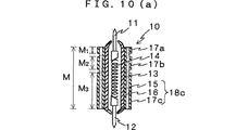
また、前述の例では、金属パイプ13の外周に形成されるキャパシタは1種類のキャパシタであったが、たとえば図10(a)に示されるように、第1の金属膜を分断して長さがM1、M2、M3の異なる長さの金属膜17a、17b、17cとすることにより、図10(b)に示されるように、異なる容量のキャパシタ18a、18b、18cを形成することができる。それぞれのキャパシタC11〜C13の容量は、全体の長さMでの容量をそれぞれの長さM1〜M3の長さに比例した大きさの容量に分配される。その結果、前述の信号用プローブとして、信号の周波数に応じた容量が要求される場合に、長さの異なる金属膜17a〜17cのうち、所望の容量の金属膜のみを金属ブロック1と接触させるようにすることにより所望の容量のキャパシタとして使用することもできる。キャパシタを形成する誘電体の材質や厚さにより、その高周波特性は異なってくるので、信号周波数に応じた所望の容量を選ぶときに、その周波数特性も変化してくる。あるいは、全ての金属膜を金属ブロックと接触させることにより、一つの誘電体材質では成し得なかった周波数特性を得ることもできる。
【0048】
【発明の効果】
本発明によれば、可動ピンにより被検査デバイスに接触させているため、被検査デバイスの電極端子との接触部分にリードの露出部分がない上に、被検査デバイスの電源電極端子に接触させる電源用プローブの周囲にキャパシタが形成されているため、被検査デバイスの電源端子に入力される直前のところでRFノイズを除去することができ、ノイズフリーの状態で検査をすることができる。すなわち、高周波・高速用デバイスを検査する場合、僅かな長さのリードでもノイズを拾いやすいため、できるだけ被検査デバイスの近くでノイズを落す必要があるが、本発明では、被検査デバイスと接触する直前の電源用プローブにキャパシタが形成されているため、非常に効果的にノイズを解消することができると共に、高速スイッチング波形出力時に発生する電源端子における電圧降下を最小限に抑えることができる。
【0049】
さらに、信号端子においても、信号の周波数に応じて、その入力前の信号用プローブに信号を減衰させず、RFノイズを減衰させる容量のキャパシタが装荷されたプローブを用いることにより、信号成分に重畳されたノイズを、被検査デバイスの端子に入る前に有効に除去することもできる。
【0050】
その結果、高周波・高速デバイスの増幅器を発振させたり、正確なデバイスの検査を行えないという問題を解決し、電源用端子および信号用端子からも完全にノイズを除去することができ、非常に安定した正確な検査をすることができる。
【0051】
なお、前述のように、電源用プローブは被検査デバイスと接触する側のみを可動ピンとして、他端側は直接ハンダ付けなどにより接続する構造にしてもよいが、接地用プローブも同様に被検査デバイスとの接触側のみに可動ピンを設ける構造にして、他端側は固定する構造でもよい。また、接地用プローブは設けられないで、たとえば細い金属細線が多数ゴム内に植立されて縦方向のみに導電し、横方向には絶縁される異方性の導電性ゴムなどを介して、金属ブロック1と被検査デバイスの接地端子とを直接接続する構造にすることもできる。
【0052】
本発明によれば、被検査デバイスの電極端子などに押圧のみで確実に接触させることができる可動ピンを有するコンタクト用のプローブに、直接キャパシタが設けられているため、高周波・高速用デバイスの特性検査をする場合に、被検査デバイスとの接触を確実にしながら、電源端子の電圧降下を防止することができると共に、電源端子や信号端子からのノイズの侵入を防止することができる。しかも、信号端子でも、その容量を調整することにより、信号を劣化させず、ノイズのみを減衰させることができる。その結果、非常に安定した検査を正確にすることができ、高周波・高速用デバイスの検査の信頼性を大幅に向上させることができる。
【0053】
【産業上の利用の可能性】
本発明は、携帯電話機などの電気機器などに組み込まれる増幅回路やミキサ回路、フィルタ回路、IC、モジュール、高速デジタル処理IC(DSP(digital signal processor)、CPU(central processing unit)、FPGA(field programmable gate array))、高速メモリ、シリアルパラレル変換IC(SER/DES(serializer/de-serializer))など、とくに高周波・高速用デバイスの検査を、プローブを接触させることにより行う分野で利用することができる。
【図面の簡単な説明】
【図1】図1(a)および1(b)は、本発明による検査治具の一実施形態を示す平面説明図および一部断面の側面説明図である。
【図2】図2(a)および2(b)は、図1に示される容量装荷型プローブの断面説明図およびその誘電体筒の斜視説明図である。
【図3】図3は、プローブに装荷するキャパシタの容量を変化させたときの、シミュレーションによる挿入損失の周波数特性である。
【図4】図4は、一例として470pFの場合の実測による挿入損失の周波数特性である。
【図5】図5は、電源用プローブに容量装荷型プローブを用いたときの等価回路図である。
【図6】図6(a)〜6(c)は、容量が1000pFと100pFの場合の電源端子における電圧降下の状態を、キャパシタがなく浮遊容量0.5pF程度だけの場合と比較して示したシミュレーションの結果である。
【図7】図7は、容量装荷型プローブの他の実施形態を示す断面説明図である。
【図8】図8は、容量装荷型プローブのさらに他の例を示す断面説明図である。
【図9】図9は、プローブを金属ブロックに固定する他の構造例を示す部分断面説明図である。
【図10】図10(a)および10(b)は、容量装荷型プローブのさらに他の実施形態を示す断面説明図および等価回路図である。
【図11】図11(a)〜11(c)は、スイッチング波形出力時に発生する電源端子における電圧の降下を説明する図である。
【図12】図12(a)および12(b)は、従来の高周波・高速用デバイスの検査治具の構成例を示す図である。[0001]
BACKGROUND OF THE INVENTION
The present invention is, for example, an amplifier circuit or a mixer circuit incorporated in a mobile phone, for high frequency / high speed (analog having a high frequency is called high frequency, and digital having a very small pulse width and pulse interval is called high speed, (In the case of high-frequency / high-speed devices that inspect semiconductor wafers, ICs, modules, etc.), the connection between the device to be inspected and the inspection equipment is ensured and the influence of external noise is minimized. The present invention relates to a capacity-loaded probe that can be used and an inspection jig using the same.
[0002]
[Prior art]
For example, when inspecting a high-frequency or high-speed device such as a semiconductor wafer, IC or module, it is easy to pick up noise in the exposed portion of the lead or the like. For example, this is also disclosed in JP 2001-99889 A, As shown in FIG. 12 (a), a spring-loaded RF signal (used to include both high frequency and high speed)
[0003]
Even with such a structure, it is easy to pick up noise at high frequency or high speed, and noise may be picked up at the portion of the spring-loaded probe in the
[0004]
On the other hand, not only the RF signal but also various medium and low frequency signals ranging from a signal close to the DC level to 100 MHz are input to the input signal terminal for inspection. Even if RF noise is input to these medium and low frequency signal terminals, accurate inspection cannot be performed. Even if these low and medium frequency input signal probes are formed in a coaxial structure, the RF noise mixed on the device side or the inspection apparatus side is directly input to the terminal of the device to be inspected. In addition, an accurate inspection cannot be performed.
[0005]
[Problems to be solved by the invention]
As described above, in an inspection jig for inspecting high-frequency or high-speed devices, the connection with the device to be inspected is made of a spring in order to make it less susceptible to noise picked up by wiring connected to the device. A contact probe having a movable pin that expands and contracts through the metal block is provided in contact with the metal block. As a result, the gap between the device to be inspected and the metal block can be securely connected, and it becomes difficult to pick up noise. Furthermore, as described above, attempts have been made to make the RF signal probe have a coaxial structure even in the metal block. On the other hand, with the progress of high frequency and high speed in recent years, there is a remarkable increase in circuit integration and package miniaturization, and metal blocks are used by increasing the number of terminals (number of electrodes) and reducing the pitch between terminals. Of course, even if the power probe in the metal block is susceptible to noise, it is very easy for noise to be superimposed, and a low-pass filter or a filter is installed on the input side to the power probe in the metal block. In the structure in which the chip capacitor is provided, there is a problem that an accurate inspection that is not affected by noise cannot be performed completely.
[0006]
In addition, due to the recent evolution of high-frequency and high-speed devices, abnormalities in inspections such as device operation errors and forced resets occur during transitions when the output changes from low to high due to changes in the input signal. As a result of intensive investigation into the cause, the present inventors have investigated the cause of the problem, and as a result, the transient time when the output voltage changes is accelerated, and as a result, the instantaneous change of the power supply current caused by the voltage change Was found to be based on causing a voltage drop at the power terminal. That is, when the power supply current increases stepwise, the
[0007]
The present invention has been made to solve such a problem. Even when testing a device that achieves high integration with high frequency and high speed and reduction in pitch between electrode probes by downsizing of the package, the power supply It is an object of the present invention to provide a capacitance loaded probe that is hardly affected by a voltage drop at a power supply terminal due to inductance while using a thin probe for connection to a terminal.
[0008]
Another object of the present invention is to perform an accurate inspection without being affected by noise even in a device that is highly integrated with high frequency and high speed, by reducing the noise according to the signal input to its terminal. It is an object of the present invention to provide an inspection jig for an inspection apparatus such as a high-capacity / high-speed device using the capacity-loaded probe that can be used.
[0009]
[Means for Solving the Problems]
A capacity loading type probe according to the present invention includes a metal pipe, a movable pin provided in the metal pipe and electrically connected to the metal pipe, and at least a protruding length protruding from one end of the metal pipe, Without the first metal film and the second metal film forming voids on the outer peripheral surface and the inner peripheral surface, respectively. Closely provided dielectric Tube When Have The dielectric A capacity loading type probe for a power source in which a cylinder is provided on an outer periphery of the metal pipe so that the metal pipe and the second metal film are electrically connected to each other. The dielectric Tube Is made of a material having a relative dielectric constant of 38 or more, and a capacitance of 50 pF or more is formed between the movable pin and the first metal film.
[0010]
Here, the movable pin means a pin whose tip can move along the axial direction, for example, if the lead wire is held and pressed by a spring or the like, and the tip is contracted by the spring or the like.
[0011]
By forming a capacitor on the outer peripheral surface of such a contact probe, when used as a probe connected to a power supply terminal or a signal terminal, a voltage drop at the power supply terminal can be prevented or noise can be removed. Can do. That is, the device to be inspected includes RF (both high frequency with a high analog frequency and high speed with a digital short pulse and a short pulse interval, and means that the analog or pulse repetition is about 1 GHz or more. For example, the voltage drop occurs when the output is switched from low to high, for example, due to the inductance of the power probe, but this capacitor can reduce the voltage drop to an extent that does not hinder the operation. . This is based on the fact that compensation by charging and discharging between the inductor and the capacitor is performed by adding the capacitor.
[0012]
Furthermore, capacitors are formed in the power supply probe and the signal probe when connecting to a power supply terminal or a signal terminal of an input signal close to a DC level or a signal terminal of a medium to low frequency signal with a small repetition of sine waves and pulses. Thus, the RF noise mixed in the power supply line and the signal line can be surely dropped by the capacitor, and a highly reliable inspection can be performed without being affected by the noise.
[0013]
Another form of the capacity loading type probe according to the present invention is a metal pipe, and is provided in the metal pipe so as to be electrically connected to the metal pipe, and at least a protrusion length protruding from one end of the metal pipe is variable. A movable pin to get, On the outer peripheral surface of the metal pipe The dielectric layer comprising: a dielectric layer provided in close contact without forming a void portion; and a first metal film provided in close contact with the outer peripheral surface of the dielectric layer without forming a void portion. Is made of a material having a relative dielectric constant of 38 or more, and a capacitance of 50 pF or more is formed between the movable pin and the first metal film. It may be a structure. The metal film provided on the inner wall and outer wall of the dielectric cylinder is formed by, for example, electroless plating. In addition, in order to form a dielectric layer with a thin film, it can be formed, for example, by sputtering or vacuum evaporation while rotating the metal pipe, or a solution obtained by dissolving a dielectric material in an organic solvent or the like It can also be formed by a sol-gel method in which it is applied, dried and fired.
[0014]
The inspection jig according to the present invention has a metal block and a movable pin whose leading end portion is movable, and penetrates the metal block so that the leading end portion of the movable pin protrudes on one surface side of the metal block. A plurality of power supply and signal probes, and the device to be inspected is pressed against the one surface side of the metal block so that the electrode terminals of the device to be inspected and the tip of the probe are in contact with each other An inspection jig for inspecting characteristics of the device to be inspected, and a power probe connected to at least some of the power terminals of the plurality of probes, The method according to any one of
[0015]
With this structure, a capacitor that bypasses the RF noise is formed around at least a part of the power supply probe and the signal probe. Therefore, the RF noise is generated immediately before the power supply terminal and signal terminal of the device under test. Even if RF noise that could not be completely removed on the wiring board (printed circuit board) side remains, it can be completely bypassed via the bypass capacitor. Removed. As a result, the intrusion of noise from the power source or medium / low frequency signal probe connected to the device via the movable pin is completely eliminated, and an accurate inspection that is not affected by the noise can be performed. Furthermore, by using a capacitance loaded probe for the power supply probe, it is possible to suppress a voltage drop at the power supply terminal caused by a change in the current inside the device, and to keep it within 10% of the general power supply voltage allowable range. Can do.
[0016]
In this specification, The repetition of a sine wave or pulse means its frequency in the case of an analog signal and its high and low repetition speed in the case of a digital signal.
[0017]
By using a capacitance loading type probe in which a capacitor having a capacitance of 50 pF or more, more preferably 100 pF or more is connected to the power probe connected to the power supply terminal of the device to be inspected, it is possible to cope with a change in input signal. The power supply voltage rarely drops by 10% or more, and high frequency noise of 400 MHz or more (200 MHz or more if 100 pF or more) can be attenuated by 10 dB or more, and high RF noise can be further attenuated. This is preferable because noise can be removed almost completely.
[0018]
DETAILED DESCRIPTION OF THE INVENTION
Next, the capacity loaded probe of the present invention and the inspection jig using the same will be described with reference to the drawings. The inspection jig according to the present invention connects the device to be inspected 20 and an inspection apparatus (not shown), and as shown in FIGS. The
[0019]
As shown in FIG. 2 (a), a cross-sectional explanatory diagram of one embodiment of the capacitive
[0020]
In the example shown in FIG. 2, a
[0021]
As shown in the perspective explanatory view of FIG. 2B, the
[0022]
In order to investigate the effect of the
[0023]
In general, if there is an insertion loss of about 10 dB, there is a great effect on noise removal, and if there is an insertion loss of about 20 dB, the influence of noise can be almost completely removed. If it is 1060 pF, noise with a frequency of about 25 MHz or more can be removed, and if it is 50 MHz or more, it can be removed almost completely. In addition, for RF noise of 1 GHz or more, it can be seen that if 100 pF, the influence of noise can be completely eliminated, and if it is 50 pF or more, the noise can be sufficiently attenuated. On the other hand, in the conventional probe without a capacitor (the stray capacitance is considered to be about 0.5 pF), the insertion loss up to 20 GHz is 2 dB or less, and it can be seen that there is almost no effect of removing RF noise. .
[0024]
On the other hand, for example, if the capacitance is 50 pF, there is almost no attenuation in the several tens of MHz band, and significant attenuation is seen at 1 GHz or more. For example, in a signal probe for inputting a signal, the frequency of the input signal is several tens of MHz or less. In the case of a signal, the present inventors have found that by using a probe loaded with a capacitor having a capacitance of about 50 pF, it is possible to input a signal from which RF noise has been removed and perform a reliable test. It was. That is, the signal probe is loaded with a capacitor having a capacity that does not attenuate the signal but attenuates only the noise at a higher frequency than the coaxial probe according to the frequency of the input signal. The present inventors have found that it is preferable to use the prepared probe.
[0025]
In order to change the capacitance, the capacitance of the
[0026]
[Table 1]
Actually, a capacitance loaded probe having a capacitor size of 530 pF shown in Table 1 was formed, and insertion loss with respect to frequency was measured. The result is shown in FIG. As a result of forming with the dimensions shown in Table 1, the actual capacitance was 470 pF. From FIG. 4, similarly to FIG. 3, an insertion loss of about 15 dB is already obtained at 50 MHz, and an insertion loss of about 20 dB or more is obtained at 200 MHz or higher, indicating that noise can be removed almost completely. In FIG. 4,
[0028]
Thus, if it is about 500 pF, since a large insertion loss can be obtained from a sufficiently low frequency to a high frequency, it is sufficient for a power source probe and a small (low frequency) input signal with a repetition close to a DC level. However, as shown in FIG. 3 described above, if it is 100 pF, there is a sufficient insertion loss at 200 MHz or more, which is practical as a power source probe.
[0029]
On the other hand, as described above, the present inventors may not be able to perform an accurate inspection due to the voltage drop at the power supply terminal during the output transient time due to the signal change due to the inductance component of the power supply probe. I found. By using a capacity loaded probe as the power probe, the voltage drop could be suppressed to 10% or less, which is not a problem. The effect of preventing a voltage drop at the power supply terminal when this capacitively loaded probe is used as a power supply probe will be described.
[0030]
When a capacity loaded probe is used as a power source probe, an equivalent circuit of a connection portion with a device under test is as shown in FIG. This power supply voltage V 1 Is 3Vdc (DC) and R 1 = 0.1Ω, L 1 = 2nH, C 1 When the current is changed to 1000 pF and 100 pF, as shown in FIG. 11B, the voltage at the power supply terminal when the current is changed from 10 mA to 50 mA stepwise (ideal state with a rise time of 0). V 2 Was investigated by simulation. The results are shown in FIGS. 6 (a) and 6 (b), respectively. FIG. 6C is a diagram showing a voltage drop when using a conventional probe in which no capacitor is loaded (assuming a stray capacitance of 0.5 pF), which is shown in FIG. 11C. Is shown on the same scale as FIGS. 6 (a) and 6 (b), and the simulation conditions are the same.
[0031]
As is apparent from FIGS. 6A to 6C, when a conventional probe without a capacitor (assuming a stray capacitance of 0.5 pF) is used, a large voltage drop of 1.32 V (44%) is obtained. When a capacitor with a capacitance of 1000 pF is loaded, the time until the voltage stabilizes becomes longer, but the amount of change in voltage is about 0.06 V, which is about 2%. Can be reduced. Note that even if the voltage pulsates for a long time, the amount of change is small, so there is no influence. Even when a 100 pF capacitor is loaded, as shown in FIG. 6B, the voltage fluctuation at the power supply terminal is larger than that at 1000 pF, but it is still about 0.18 V and about 6%. It is small and can sufficiently clear 10% which is generally regarded as the limit of variation. That is, by using a probe loaded with a capacity of 100 pF or more as the power supply probe, it is possible to suppress voltage fluctuations to such an extent that they do not hinder even a very rapid change in current.
[0032]
Thus, by using the capacity loading type probe as the power source probe, the fluctuation of the voltage at the power source terminal can be prevented, for example, from one viewpoint, the inductance of the power source probe and the loaded capacity This is probably because the voltage is compensated by the action of charging and discharging. As a result, even if the output of the device under test instantaneously changes from low to high or from high to low depending on the signal, voltage fluctuations at the power supply terminal can be suppressed. The possibility of causing a reset can be eliminated, and a very stable test can be performed. In the high-frequency / high-speed device, in order to minimize the routing by wiring, as described above, a large number of power supply terminals are formed even for one device. Therefore, even if a single power source probe does not secure this size of capacity, the loaded capacity can be increased by using a large number of power source probes in parallel. On the other hand, the voltage drop suppression and noise removal effects by the power supply probe can be achieved without using the capacity loading type probe for all the power supply probes.
[0033]
As described above, in order to use such a capacity loaded
[0034]
On the other hand, in the signal probe, there are various signal lines, ranging from those close to the DC level to RF signals of 1 GHz or higher, and RF noise of 1 GHz or higher is also superimposed on medium and low frequency signal lines of about 100 MHz or lower. In some cases, it is desirable to selectively remove these noises. Therefore, noise can be reliably removed and a highly reliable test can be performed by using a capacitance loaded probe with a capacitance selected for each signal terminal according to the frequency of the applied signal. .
[0035]
For example, when using the above-described dielectric cylinder, barium titanate (relative dielectric constant of about 700 to 20000) and strontium titanate (relative dielectric constant of about 1500 to 4000) are used as the dielectric for such a capacitance loaded capacitor. In addition to those having a high relative dielectric constant such as), sintered ceramics such as high dielectric ceramics (relative dielectric constant of about 10 to 50) and alumina (relative dielectric constant 9 to 10) can be used. By using a material with a high relative dielectric constant, such as barium titanate or strontium titanate, high frequency noise can be generated even with very small power probes with inner and outer diameters of 0.3 mm and 0.6 mm and lengths of about 6 mm. It is preferable because a large capacitance of about 1000 pF or more that can be almost completely bypassed can be formed, and even low-frequency noise can be easily removed.
[0036]
Further, as will be described later, for example, a thin film can be formed directly on the outer surface of the
[0037]
When the dielectric cylinder type is used, since the capacitor does not flow current, the conductivity of the electrode is not a problem. However, if the dielectric and the electrode metal are not in close contact, the gap having a small dielectric constant Therefore, it is preferable that a metal film is provided in close contact with the inner peripheral surface and the outer peripheral surface of the
[0038]
FIG. 7 shows an example in which the dielectric
[0039]
In the case of forming a film by sputtering or vacuum evaporation, the film can be formed on the entire surface by forming the film while rotating the
[0040]
As shown in FIG. 2A, the
[0041]
Further, as shown in FIG. 2A, the
[0042]
The
[0043]
For example, if the
[0044]
The
[0045]
The
[0046]
In the example shown in FIG. 1B, the structure is such that one end of the probe is fixed by the
[0047]
In the above example, the capacitor formed on the outer periphery of the
[0048]
【The invention's effect】
According to the present invention, since the movable pin is brought into contact with the device to be inspected, there is no exposed portion of the lead in the contact portion with the electrode terminal of the device to be inspected, and the power source is brought into contact with the power electrode terminal of the device to be inspected. Since the capacitor is formed around the probe, RF noise can be removed immediately before being input to the power supply terminal of the device to be inspected, and inspection can be performed in a noise-free state. That is, when inspecting a device for high frequency and high speed, it is easy to pick up noise even with a lead having a small length, so it is necessary to reduce noise as close as possible to the device to be inspected. Since the capacitor is formed in the immediately preceding power supply probe, noise can be eliminated very effectively, and voltage drop at the power supply terminal that occurs when a high-speed switching waveform is output can be minimized.
[0049]
Furthermore, at the signal terminal, depending on the frequency of the signal, the signal probe before input does not attenuate the signal, but a probe loaded with a capacitor having a capacity to attenuate RF noise is used to superimpose the signal component. The generated noise can be effectively removed before entering the terminal of the device under test.
[0050]
As a result, it is possible to solve the problem of not oscillating amplifiers for high frequency and high speed devices or to perform accurate device inspection, and noise can be completely removed from power supply terminals and signal terminals. Accurate inspection can be done.
[0051]
As described above, the power probe may have a structure in which only the side in contact with the device to be inspected is a movable pin and the other end is directly connected by soldering or the like, but the grounding probe is similarly inspected. The movable pin may be provided only on the contact side with the device, and the other end may be fixed. Also, no grounding probe is provided, for example, through the use of anisotropic conductive rubber that is electrically conductive only in the vertical direction and is insulated in the horizontal direction, with a number of thin fine metal wires planted in the rubber. The
[0052]
According to the present invention, since a capacitor is directly provided on a contact probe having a movable pin that can be reliably brought into contact with an electrode terminal or the like of a device to be inspected, the characteristics of a high-frequency / high-speed device can be obtained. When inspecting, while ensuring contact with the device to be inspected, it is possible to prevent a voltage drop at the power supply terminal and to prevent noise from entering from the power supply terminal and the signal terminal. Moreover, by adjusting the capacity of the signal terminal, it is possible to attenuate only noise without degrading the signal. As a result, a very stable inspection can be made accurate and the reliability of the inspection of the high frequency / high speed device can be greatly improved.
[0053]
[Possibility of industrial use]
The present invention relates to an amplifier circuit, a mixer circuit, a filter circuit, an IC, a module, a high-speed digital processing IC (DSP (digital signal processor), a CPU (central processing unit), an FPGA (field programmable) incorporated in an electric device such as a cellular phone. gate array)), high-speed memory, serial / parallel conversion IC (SER / DES (serializer / de-serializer)), etc., particularly in the field where high-frequency / high-speed devices are inspected by contacting them. .
[Brief description of the drawings]
FIGS. 1 (a) and 1 (b) are a plane explanatory view and a partial cross-sectional side view showing an embodiment of an inspection jig according to the present invention.
2 (a) and 2 (b) are a cross-sectional explanatory view of the capacitively loaded probe shown in FIG. 1 and a perspective explanatory view of its dielectric cylinder.
FIG. 3 is a frequency characteristic of insertion loss by simulation when the capacitance of a capacitor loaded on the probe is changed.
FIG. 4 is a frequency characteristic of insertion loss measured in the case of 470 pF as an example.
FIG. 5 is an equivalent circuit diagram when a capacitively loaded probe is used as a power source probe.
6 (a) to 6 (c) show the state of voltage drop at the power supply terminal when the capacitance is 1000pF and 100pF, compared with the case where there is no capacitor and only stray capacitance is about 0.5pF. It is the result of the simulation.
FIG. 7 is a cross-sectional explanatory view showing another embodiment of the capacity loaded probe.
FIG. 8 is a cross-sectional explanatory view showing still another example of the capacity loaded probe.
FIG. 9 is a partial cross-sectional explanatory view showing another structural example for fixing the probe to the metal block.
FIGS. 10A and 10B are a cross-sectional explanatory view and an equivalent circuit diagram showing still another embodiment of the capacity loaded probe.
FIGS. 11A to 11C are diagrams for explaining a voltage drop at a power supply terminal that occurs when a switching waveform is output. FIG.
FIGS. 12A and 12B are diagrams showing a configuration example of an inspection jig of a conventional high-frequency / high-speed device.
Claims (6)
Priority Applications (1)
| Application Number | Priority Date | Filing Date | Title |
|---|---|---|---|
| JP2003566566A JP4707322B2 (en) | 2002-02-07 | 2003-02-06 | Capacity loaded probe and inspection jig using the same |
Applications Claiming Priority (4)
| Application Number | Priority Date | Filing Date | Title |
|---|---|---|---|
| JP2002031389 | 2002-02-07 | ||
| JP2002031389 | 2002-02-07 | ||
| JP2003566566A JP4707322B2 (en) | 2002-02-07 | 2003-02-06 | Capacity loaded probe and inspection jig using the same |
| PCT/JP2003/001277 WO2003067268A1 (en) | 2002-02-07 | 2003-02-06 | Capacity load type probe, and test jig using the same |
Publications (2)
| Publication Number | Publication Date |
|---|---|
| JPWO2003067268A1 JPWO2003067268A1 (en) | 2005-06-02 |
| JP4707322B2 true JP4707322B2 (en) | 2011-06-22 |
Family
ID=27677932
Family Applications (1)
| Application Number | Title | Priority Date | Filing Date |
|---|---|---|---|
| JP2003566566A Expired - Fee Related JP4707322B2 (en) | 2002-02-07 | 2003-02-06 | Capacity loaded probe and inspection jig using the same |
Country Status (8)
| Country | Link |
|---|---|
| US (1) | US7233156B2 (en) |
| EP (1) | EP1482313B1 (en) |
| JP (1) | JP4707322B2 (en) |
| AU (1) | AU2003207078A1 (en) |
| DE (1) | DE60317638T2 (en) |
| MY (1) | MY139934A (en) |
| TW (1) | TWI278631B (en) |
| WO (1) | WO2003067268A1 (en) |
Families Citing this family (27)
| Publication number | Priority date | Publication date | Assignee | Title |
|---|---|---|---|---|
| JP4251855B2 (en) * | 2002-11-19 | 2009-04-08 | 株式会社ヨコオ | Manufacturing method of inspection jigs for high frequency and high speed devices |
| JP2005127891A (en) * | 2003-10-24 | 2005-05-19 | Yokowo Co Ltd | Inductor loaded inspecting probe |
| JP4689196B2 (en) | 2003-11-05 | 2011-05-25 | 日本発條株式会社 | Conductive contact holder, conductive contact unit |
| US7202678B2 (en) * | 2003-12-18 | 2007-04-10 | Lecroy Corporation | Resistive probe tips |
| EP1761104A4 (en) * | 2004-06-03 | 2016-12-28 | Olympus Corp | Electrostatic capacity type ultrasonic vibrator, manufacturing method thereof, and electrostatic capacity type ultrasonic probe |
| JP4757531B2 (en) * | 2005-04-28 | 2011-08-24 | 日本発條株式会社 | Conductive contact holder and conductive contact unit |
| WO2007097356A1 (en) * | 2006-02-21 | 2007-08-30 | Luzcom Inc. | Ultrafine coaxial line and ultrafine coaxial barrel and production method for them |
| US20080106292A1 (en) * | 2006-11-02 | 2008-05-08 | Corad Technology, Inc. | Probe card having cantilever probes |
| JP2008145238A (en) * | 2006-12-08 | 2008-06-26 | Micronics Japan Co Ltd | Electrical connection apparatus and electric connection device using it |
| US20080238461A1 (en) * | 2007-04-02 | 2008-10-02 | Ken Skala | Multi-type test interface system and method |
| US7816932B2 (en) | 2008-02-21 | 2010-10-19 | Teradyne, Inc. | Test system with high frequency interposer |
| US20100181847A1 (en) * | 2009-01-22 | 2010-07-22 | Shen-Yu Huang | Method for reducing supply voltage drop in digital circuit block and related layout architecture |
| MY155882A (en) | 2009-03-10 | 2015-12-15 | Johnstech Int Corp | Electrically conductive pins for microcircuit tester |
| US20130002285A1 (en) | 2010-03-10 | 2013-01-03 | Johnstech International Corporation | Electrically Conductive Pins For Microcircuit Tester |
| US9007082B2 (en) | 2010-09-07 | 2015-04-14 | Johnstech International Corporation | Electrically conductive pins for microcircuit tester |
| TWI534432B (en) | 2010-09-07 | 2016-05-21 | 瓊斯科技國際公司 | Electrically conductive pins for microcircuit tester |
| US8723542B2 (en) * | 2011-04-25 | 2014-05-13 | Cheng Uei Precision Industry Co., Ltd. | Testing jig for pogo pin connector |
| KR102016427B1 (en) | 2013-09-10 | 2019-09-02 | 삼성전자주식회사 | Pogo pin and probe card including the same |
| KR101552553B1 (en) * | 2014-09-23 | 2015-10-01 | 리노공업주식회사 | A contact probe for the test device |
| JP2016212040A (en) * | 2015-05-13 | 2016-12-15 | 富士通コンポーネント株式会社 | contact |
| KR101906575B1 (en) * | 2016-11-29 | 2018-10-11 | 리노공업주식회사 | Camera module test device |
| JP2020504309A (en) * | 2017-01-12 | 2020-02-06 | フォームファクター, インコーポレイテッド | Vertical probe head shield |
| CN106840768B (en) * | 2017-01-19 | 2024-01-30 | 中国科学院南京土壤研究所 | Organic pollutant in-situ curing and collecting device and application thereof |
| JP6663084B2 (en) * | 2017-07-13 | 2020-03-11 | 日本発條株式会社 | Probe unit |
| CN108982926A (en) * | 2018-07-25 | 2018-12-11 | 天地融电子(天津)有限公司 | A kind of test fixture |
| TWI680300B (en) * | 2019-03-18 | 2019-12-21 | 中華精測科技股份有限公司 | Probe card device and conductive probe thereof |
| KR102235724B1 (en) * | 2020-04-10 | 2021-04-02 | 주식회사 메가터치 | Metal material manufacturing method for electronic component, the metal material and pogo pin manufactured by the metal material |
Family Cites Families (22)
| Publication number | Priority date | Publication date | Assignee | Title |
|---|---|---|---|---|
| JPS5834364A (en) | 1981-08-24 | 1983-02-28 | Nissan Motor Co Ltd | Probe |
| JPS58175273A (en) | 1982-04-07 | 1983-10-14 | 沖電気工業株式会社 | Coaxial movable contact probe |
| JPS6156981A (en) | 1984-08-27 | 1986-03-22 | Nec Corp | Semiconductor inspecting device |
| US4724180A (en) * | 1985-08-05 | 1988-02-09 | Teradyne, Inc. | Electrically shielded connectors |
| JPH0521020Y2 (en) * | 1985-12-05 | 1993-05-31 | ||
| JPH01128536A (en) | 1987-11-13 | 1989-05-22 | Hitachi Ltd | Probe for measuring semiconductor element |
| JPH02133280U (en) | 1989-04-06 | 1990-11-06 | ||
| US5512838A (en) * | 1992-09-03 | 1996-04-30 | Hewlett-Packard Company | Probe with reduced input capacitance |
| JPH06216205A (en) * | 1993-01-13 | 1994-08-05 | Tokyo Electron Yamanashi Kk | Probe card interface device |
| US5532613A (en) * | 1993-04-16 | 1996-07-02 | Tokyo Electron Kabushiki Kaisha | Probe needle |
| US5525911A (en) * | 1993-08-04 | 1996-06-11 | Tokyo Electron Limited | Vertical probe tester card with coaxial probes |
| JPH07260878A (en) | 1994-03-18 | 1995-10-13 | Fujitsu Ltd | Test station |
| US6046597A (en) * | 1995-10-04 | 2000-04-04 | Oz Technologies, Inc. | Test socket for an IC device |
| JPH10213583A (en) | 1997-01-28 | 1998-08-11 | Wako Pure Chem Ind Ltd | Urine test paper feeding device |
| JPH10213593A (en) * | 1997-01-29 | 1998-08-11 | Alps Electric Co Ltd | Contact and connecting jig using the same |
| JP2000266779A (en) * | 1999-03-18 | 2000-09-29 | Toshiba Corp | Multiprobe unit |
| JP2001042002A (en) | 1999-07-30 | 2001-02-16 | Advantest Corp | Contact board for calibrating timing of semiconductor device tester and probe touching contact board |
| JP2001099889A (en) * | 1999-09-29 | 2001-04-13 | Yokowo Co Ltd | Inspection equipment for high frequency circuit |
| US6700397B2 (en) * | 2000-07-13 | 2004-03-02 | The Micromanipulator Company, Inc. | Triaxial probe assembly |
| US6784679B2 (en) * | 2002-09-30 | 2004-08-31 | Teradyne, Inc. | Differential coaxial contact array for high-density, high-speed signals |
| JP4251855B2 (en) * | 2002-11-19 | 2009-04-08 | 株式会社ヨコオ | Manufacturing method of inspection jigs for high frequency and high speed devices |
| US6727716B1 (en) * | 2002-12-16 | 2004-04-27 | Newport Fab, Llc | Probe card and probe needle for high frequency testing |
-
2003
- 2003-02-06 TW TW092102373A patent/TWI278631B/en not_active IP Right Cessation
- 2003-02-06 AU AU2003207078A patent/AU2003207078A1/en not_active Abandoned
- 2003-02-06 US US10/503,669 patent/US7233156B2/en not_active Expired - Fee Related
- 2003-02-06 WO PCT/JP2003/001277 patent/WO2003067268A1/en active IP Right Grant
- 2003-02-06 EP EP03703239A patent/EP1482313B1/en not_active Expired - Fee Related
- 2003-02-06 JP JP2003566566A patent/JP4707322B2/en not_active Expired - Fee Related
- 2003-02-06 DE DE60317638T patent/DE60317638T2/en not_active Expired - Lifetime
- 2003-02-07 MY MYPI20030415A patent/MY139934A/en unknown
Also Published As
| Publication number | Publication date |
|---|---|
| WO2003067268A1 (en) | 2003-08-14 |
| EP1482313B1 (en) | 2007-11-21 |
| US20050088189A1 (en) | 2005-04-28 |
| US7233156B2 (en) | 2007-06-19 |
| AU2003207078A1 (en) | 2003-09-02 |
| TW200303423A (en) | 2003-09-01 |
| DE60317638D1 (en) | 2008-01-03 |
| DE60317638T2 (en) | 2008-10-30 |
| JPWO2003067268A1 (en) | 2005-06-02 |
| EP1482313A4 (en) | 2005-10-12 |
| TWI278631B (en) | 2007-04-11 |
| MY139934A (en) | 2009-11-30 |
| EP1482313A1 (en) | 2004-12-01 |
Similar Documents
| Publication | Publication Date | Title |
|---|---|---|
| JP4707322B2 (en) | Capacity loaded probe and inspection jig using the same | |
| JP4251855B2 (en) | Manufacturing method of inspection jigs for high frequency and high speed devices | |
| EP0551564B1 (en) | Non-contact test probe | |
| US6727716B1 (en) | Probe card and probe needle for high frequency testing | |
| TWI452307B (en) | Test socket | |
| US7368928B2 (en) | Vertical type high frequency probe card | |
| US7259577B2 (en) | Shielded probe apparatus for probing semiconductor wafer | |
| JP4535828B2 (en) | Inspection unit manufacturing method | |
| US20010026166A1 (en) | Probe contactor and production method thereof | |
| JP2004325305A (en) | Ic socket | |
| JP2001159642A (en) | Contact structure with silicon finger contactor and total assembly structure using it | |
| JP2001099889A (en) | Inspection equipment for high frequency circuit | |
| WO1999041812A1 (en) | Ic socket | |
| US20030193341A1 (en) | Systems and methods for wideband differential probing of variably spaced probe points | |
| JPH06140484A (en) | Probe card | |
| JP2005049163A (en) | Test jig and probe for test apparatus of device for high frequency and high speed | |
| US6831452B2 (en) | Systems and methods for wideband single-end probing of variabily spaced probe points | |
| JP2010122139A (en) | High-frequency probe card | |
| JP2006344662A (en) | Probe card, dc characteristic measuring method using this, and semiconductor device | |
| TWI397695B (en) | Probing apparatus for integrated circuit testing | |
| JP4251854B2 (en) | Inspection jig for high frequency and high speed devices | |
| JP2003232834A (en) | Inspection method of high-frequency high-speed device and inspection tool | |
| JP2001242195A (en) | Contact structure | |
| KR100795909B1 (en) | Probe card of semiconductor test apparatus | |
| US20120013358A1 (en) | Probing apparatus for integrated circuit testing |
Legal Events
| Date | Code | Title | Description |
|---|---|---|---|
| A621 | Written request for application examination |
Free format text: JAPANESE INTERMEDIATE CODE: A621 Effective date: 20060119 |
|
| A131 | Notification of reasons for refusal |
Free format text: JAPANESE INTERMEDIATE CODE: A131 Effective date: 20080115 |
|
| A521 | Written amendment |
Free format text: JAPANESE INTERMEDIATE CODE: A523 Effective date: 20080312 |
|
| A02 | Decision of refusal |
Free format text: JAPANESE INTERMEDIATE CODE: A02 Effective date: 20090421 |
|
| A521 | Written amendment |
Free format text: JAPANESE INTERMEDIATE CODE: A523 Effective date: 20090713 |
|
| A911 | Transfer to examiner for re-examination before appeal (zenchi) |
Free format text: JAPANESE INTERMEDIATE CODE: A911 Effective date: 20090728 |
|
| A912 | Re-examination (zenchi) completed and case transferred to appeal board |
Free format text: JAPANESE INTERMEDIATE CODE: A912 Effective date: 20090828 |
|
| A521 | Written amendment |
Free format text: JAPANESE INTERMEDIATE CODE: A523 Effective date: 20110209 |
|
| A61 | First payment of annual fees (during grant procedure) |
Free format text: JAPANESE INTERMEDIATE CODE: A61 Effective date: 20110315 |
|
| R250 | Receipt of annual fees |
Free format text: JAPANESE INTERMEDIATE CODE: R250 |
|
| LAPS | Cancellation because of no payment of annual fees |