JP4707056B2 - Integrated electronic component and integrated electronic component manufacturing method - Google Patents
Integrated electronic component and integrated electronic component manufacturing methodInfo
- Publication number
- JP4707056B2 JP4707056B2 JP2005252596A JP2005252596A JP4707056B2 JP 4707056 B2 JP4707056 B2 JP 4707056B2 JP 2005252596 A JP2005252596 A JP 2005252596A JP 2005252596 A JP2005252596 A JP 2005252596A JP 4707056 B2 JP4707056 B2 JP 4707056B2
- Authority
- JP
- Japan
- Prior art keywords
- substrate
- coil
- wiring
- integrated electronic
- electronic component
- Prior art date
- Legal status (The legal status is an assumption and is not a legal conclusion. Google has not performed a legal analysis and makes no representation as to the accuracy of the status listed.)
- Active
Links
- 238000004519 manufacturing process Methods 0.000 title description 18
- 239000000758 substrate Substances 0.000 claims description 133
- 239000004020 conductor Substances 0.000 claims description 113
- 238000005260 corrosion Methods 0.000 claims description 16
- 230000007797 corrosion Effects 0.000 claims description 16
- 239000011347 resin Substances 0.000 claims description 12
- 229920005989 resin Polymers 0.000 claims description 12
- 238000007789 sealing Methods 0.000 claims description 11
- 238000000034 method Methods 0.000 description 63
- 238000009713 electroplating Methods 0.000 description 40
- 239000003990 capacitor Substances 0.000 description 36
- 230000008569 process Effects 0.000 description 24
- 239000000463 material Substances 0.000 description 19
- 238000012986 modification Methods 0.000 description 17
- 230000004048 modification Effects 0.000 description 17
- 239000000919 ceramic Substances 0.000 description 13
- 230000003071 parasitic effect Effects 0.000 description 13
- 230000001629 suppression Effects 0.000 description 9
- VYPSYNLAJGMNEJ-UHFFFAOYSA-N silicon dioxide Inorganic materials O=[Si]=O VYPSYNLAJGMNEJ-UHFFFAOYSA-N 0.000 description 8
- 238000005516 engineering process Methods 0.000 description 7
- 239000004065 semiconductor Substances 0.000 description 7
- XUIMIQQOPSSXEZ-UHFFFAOYSA-N Silicon Chemical compound [Si] XUIMIQQOPSSXEZ-UHFFFAOYSA-N 0.000 description 6
- 230000015572 biosynthetic process Effects 0.000 description 6
- 239000003989 dielectric material Substances 0.000 description 6
- 229910052710 silicon Inorganic materials 0.000 description 6
- 239000010703 silicon Substances 0.000 description 6
- 239000000470 constituent Substances 0.000 description 5
- 229910052802 copper Inorganic materials 0.000 description 5
- 239000011521 glass Substances 0.000 description 5
- 229910052737 gold Inorganic materials 0.000 description 5
- 229920002577 polybenzoxazole Polymers 0.000 description 5
- 239000010453 quartz Substances 0.000 description 5
- 239000003566 sealing material Substances 0.000 description 5
- 229910052709 silver Inorganic materials 0.000 description 5
- 239000011248 coating agent Substances 0.000 description 4
- 238000000576 coating method Methods 0.000 description 4
- 238000013461 design Methods 0.000 description 4
- 239000011159 matrix material Substances 0.000 description 4
- 238000005459 micromachining Methods 0.000 description 4
- 229920002120 photoresistant polymer Polymers 0.000 description 4
- 239000004642 Polyimide Substances 0.000 description 3
- 229910052581 Si3N4 Inorganic materials 0.000 description 3
- 238000004891 communication Methods 0.000 description 3
- 239000012776 electronic material Substances 0.000 description 3
- 239000007769 metal material Substances 0.000 description 3
- TWNQGVIAIRXVLR-UHFFFAOYSA-N oxo(oxoalumanyloxy)alumane Chemical compound O=[Al]O[Al]=O TWNQGVIAIRXVLR-UHFFFAOYSA-N 0.000 description 3
- 229920001721 polyimide Polymers 0.000 description 3
- HQVNEWCFYHHQES-UHFFFAOYSA-N silicon nitride Chemical compound N12[Si]34N5[Si]62N3[Si]51N64 HQVNEWCFYHHQES-UHFFFAOYSA-N 0.000 description 3
- 229910052814 silicon oxide Inorganic materials 0.000 description 3
- 238000004544 sputter deposition Methods 0.000 description 3
- 229910017103 Fe—Al—O Inorganic materials 0.000 description 2
- 229910013641 LiNbO 3 Inorganic materials 0.000 description 2
- 229910004298 SiO 2 Inorganic materials 0.000 description 2
- 229910045601 alloy Inorganic materials 0.000 description 2
- 239000000956 alloy Substances 0.000 description 2
- UMIVXZPTRXBADB-UHFFFAOYSA-N benzocyclobutene Chemical class C1=CC=C2CCC2=C1 UMIVXZPTRXBADB-UHFFFAOYSA-N 0.000 description 2
- 238000001312 dry etching Methods 0.000 description 2
- 230000002500 effect on skin Effects 0.000 description 2
- 230000005672 electromagnetic field Effects 0.000 description 2
- 230000005674 electromagnetic induction Effects 0.000 description 2
- 230000006698 induction Effects 0.000 description 2
- 239000012212 insulator Substances 0.000 description 2
- 239000000696 magnetic material Substances 0.000 description 2
- 229910052751 metal Inorganic materials 0.000 description 2
- 239000002184 metal Substances 0.000 description 2
- 238000000059 patterning Methods 0.000 description 2
- 238000012545 processing Methods 0.000 description 2
- 230000009467 reduction Effects 0.000 description 2
- 229910052707 ruthenium Inorganic materials 0.000 description 2
- 238000004528 spin coating Methods 0.000 description 2
- 238000000992 sputter etching Methods 0.000 description 2
- 239000010936 titanium Substances 0.000 description 2
- 238000001039 wet etching Methods 0.000 description 2
- GWEVSGVZZGPLCZ-UHFFFAOYSA-N Titan oxide Chemical compound O=[Ti]=O GWEVSGVZZGPLCZ-UHFFFAOYSA-N 0.000 description 1
- 229910052782 aluminium Inorganic materials 0.000 description 1
- 230000003247 decreasing effect Effects 0.000 description 1
- 238000000151 deposition Methods 0.000 description 1
- 238000011161 development Methods 0.000 description 1
- 238000010586 diagram Methods 0.000 description 1
- 238000009826 distribution Methods 0.000 description 1
- 238000001704 evaporation Methods 0.000 description 1
- 230000004907 flux Effects 0.000 description 1
- 230000010354 integration Effects 0.000 description 1
- 239000007788 liquid Substances 0.000 description 1
- 239000012528 membrane Substances 0.000 description 1
- 229910021421 monocrystalline silicon Inorganic materials 0.000 description 1
- BPUBBGLMJRNUCC-UHFFFAOYSA-N oxygen(2-);tantalum(5+) Chemical compound [O-2].[O-2].[O-2].[O-2].[O-2].[Ta+5].[Ta+5] BPUBBGLMJRNUCC-UHFFFAOYSA-N 0.000 description 1
- 238000004806 packaging method and process Methods 0.000 description 1
- 238000000926 separation method Methods 0.000 description 1
- 239000002210 silicon-based material Substances 0.000 description 1
- 239000007787 solid Substances 0.000 description 1
- 238000005507 spraying Methods 0.000 description 1
- 229910001936 tantalum oxide Inorganic materials 0.000 description 1
- OGIDPMRJRNCKJF-UHFFFAOYSA-N titanium oxide Inorganic materials [Ti]=O OGIDPMRJRNCKJF-UHFFFAOYSA-N 0.000 description 1
- 239000013585 weight reducing agent Substances 0.000 description 1
- 238000004804 winding Methods 0.000 description 1
Images


Classifications
-
- H—ELECTRICITY
- H01—ELECTRIC ELEMENTS
- H01L—SEMICONDUCTOR DEVICES NOT COVERED BY CLASS H10
- H01L27/00—Devices consisting of a plurality of semiconductor or other solid-state components formed in or on a common substrate
- H01L27/02—Devices consisting of a plurality of semiconductor or other solid-state components formed in or on a common substrate including semiconductor components specially adapted for rectifying, oscillating, amplifying or switching and having potential barriers; including integrated passive circuit elements having potential barriers
- H01L27/04—Devices consisting of a plurality of semiconductor or other solid-state components formed in or on a common substrate including semiconductor components specially adapted for rectifying, oscillating, amplifying or switching and having potential barriers; including integrated passive circuit elements having potential barriers the substrate being a semiconductor body
- H01L27/06—Devices consisting of a plurality of semiconductor or other solid-state components formed in or on a common substrate including semiconductor components specially adapted for rectifying, oscillating, amplifying or switching and having potential barriers; including integrated passive circuit elements having potential barriers the substrate being a semiconductor body including a plurality of individual components in a non-repetitive configuration
- H01L27/0688—Integrated circuits having a three-dimensional layout
-
- H—ELECTRICITY
- H03—ELECTRONIC CIRCUITRY
- H03H—IMPEDANCE NETWORKS, e.g. RESONANT CIRCUITS; RESONATORS
- H03H7/00—Multiple-port networks comprising only passive electrical elements as network components
- H03H7/38—Impedance-matching networks
-
- H—ELECTRICITY
- H01—ELECTRIC ELEMENTS
- H01F—MAGNETS; INDUCTANCES; TRANSFORMERS; SELECTION OF MATERIALS FOR THEIR MAGNETIC PROPERTIES
- H01F17/00—Fixed inductances of the signal type
- H01F17/0006—Printed inductances
-
- H—ELECTRICITY
- H01—ELECTRIC ELEMENTS
- H01L—SEMICONDUCTOR DEVICES NOT COVERED BY CLASS H10
- H01L23/00—Details of semiconductor or other solid state devices
- H01L23/52—Arrangements for conducting electric current within the device in operation from one component to another, i.e. interconnections, e.g. wires, lead frames
- H01L23/522—Arrangements for conducting electric current within the device in operation from one component to another, i.e. interconnections, e.g. wires, lead frames including external interconnections consisting of a multilayer structure of conductive and insulating layers inseparably formed on the semiconductor body
- H01L23/5227—Inductive arrangements or effects of, or between, wiring layers
-
- H—ELECTRICITY
- H01—ELECTRIC ELEMENTS
- H01L—SEMICONDUCTOR DEVICES NOT COVERED BY CLASS H10
- H01L2924/00—Indexing scheme for arrangements or methods for connecting or disconnecting semiconductor or solid-state bodies as covered by H01L24/00
- H01L2924/0001—Technical content checked by a classifier
- H01L2924/0002—Not covered by any one of groups H01L24/00, H01L24/00 and H01L2224/00
-
- H—ELECTRICITY
- H01—ELECTRIC ELEMENTS
- H01L—SEMICONDUCTOR DEVICES NOT COVERED BY CLASS H10
- H01L2924/00—Indexing scheme for arrangements or methods for connecting or disconnecting semiconductor or solid-state bodies as covered by H01L24/00
- H01L2924/095—Indexing scheme for arrangements or methods for connecting or disconnecting semiconductor or solid-state bodies as covered by H01L24/00 with a principal constituent of the material being a combination of two or more materials provided in the groups H01L2924/013 - H01L2924/0715
- H01L2924/097—Glass-ceramics, e.g. devitrified glass
- H01L2924/09701—Low temperature co-fired ceramic [LTCC]
-
- H—ELECTRICITY
- H01—ELECTRIC ELEMENTS
- H01L—SEMICONDUCTOR DEVICES NOT COVERED BY CLASS H10
- H01L2924/00—Indexing scheme for arrangements or methods for connecting or disconnecting semiconductor or solid-state bodies as covered by H01L24/00
- H01L2924/30—Technical effects
- H01L2924/301—Electrical effects
- H01L2924/3011—Impedance
Landscapes
- Engineering & Computer Science (AREA)
- Power Engineering (AREA)
- Microelectronics & Electronic Packaging (AREA)
- Physics & Mathematics (AREA)
- Condensed Matter Physics & Semiconductors (AREA)
- General Physics & Mathematics (AREA)
- Computer Hardware Design (AREA)
- Coils Or Transformers For Communication (AREA)
- Semiconductor Integrated Circuits (AREA)
- Manufacturing Cores, Coils, And Magnets (AREA)
- Internal Circuitry In Semiconductor Integrated Circuit Devices (AREA)
Description
本発明は、インダクタを含む複数の受動部品が集積化された集積型電子部品およびその製造方法に関する。 The present invention relates to an integrated electronic component in which a plurality of passive components including an inductor are integrated, and a manufacturing method thereof.
携帯端末などの具備するRF(radio frequency)システムないしRF回路においては、一般に、高性能化、小型化、軽量化等を図るべく、高周波モジュール用デバイスとしてIPD(integrated passive device)が採用される。IPDは、必要な所定の受動部品(インダクタ,キャパシタ,抵抗,フィルタなど)が集積化されたものであり、受動部品としてインダクタを含む場合が多い。インダクタは、例えばキャパシタと比較してQ値が低い傾向にあり、IPDがインダクタを含む場合、当該IPD全体のQ値も低くなりやすい。そのため、インダクタを含む従来のIPDについては、高Q値化への要望がある。一方、RFシステムの利用周波数帯域の高周波数化に伴い、IPDについては、当該高周波数化への対応も求められている。このようなIPDに関する技術については、例えば下記の特許文献1,2および非特許文献1,2に記載されている。
In an RF (radio frequency) system or an RF circuit provided in a portable terminal or the like, an IPD (integrated passive device) is generally used as a high-frequency module device in order to achieve high performance, miniaturization, weight reduction, and the like. The IPD is an integration of necessary predetermined passive components (inductors, capacitors, resistors, filters, etc.) and often includes an inductor as a passive component. Inductors tend to have a lower Q value than, for example, capacitors, and when an IPD includes an inductor, the Q value of the entire IPD tends to be lower. Therefore, there is a demand for a high Q value for a conventional IPD including an inductor. On the other hand, with the increase in the frequency of the RF system, the IPD is also required to cope with the higher frequency. Such IPD technology is described in, for example,
例えば非特許文献1に記載されているように、LTCC(low-temperature co-fired ceramic)技術を利用して製造されるIPDが知られている。LTCC技術を利用して製造されるIPDでは、多層セラミック基板内に複数の受動部品が内蔵されて集積化される。インダクタについては、そのインダクタンスの増大を目的として、多層セラミック基板の複数層にわたって複数のコイルが多段配置された形態で形成される場合がある。インダクタのインダクタンスが高いほど、当該インダクタのQ値は高い傾向にあり、従って、当該インダクタを含むIPD全体のQ値の向上の観点から好ましい。 For example, as described in Non-Patent Document 1, an IPD manufactured using LTCC (low-temperature co-fired ceramic) technology is known. In an IPD manufactured using LTCC technology, a plurality of passive components are built in and integrated in a multilayer ceramic substrate. An inductor may be formed in a form in which a plurality of coils are arranged in multiple stages over a plurality of layers of a multilayer ceramic substrate for the purpose of increasing the inductance. The higher the inductance of the inductor, the higher the Q value of the inductor. Therefore, it is preferable from the viewpoint of improving the Q value of the entire IPD including the inductor.
しかしながら、LTCC技術を利用して製造されるIPDにおけるインダクタの各コイルは、セラミックに包囲されており且つセラミックの誘電率は比較的大きいので、当該インダクタについては、有意な寄生容量が生じてしまう。インダクタの寄生容量が大きいほど、当該インダクタのQ値の向上の観点からは好ましくないことが知られている。そのため、LTCC技術を利用して製造されるIPDでは、それに内蔵されるインダクタについて、充分にQ値を向上することができない場合がある。 However, each coil of the inductor in the IPD manufactured using the LTCC technology is surrounded by ceramic and the dielectric constant of the ceramic is relatively large, so that a significant parasitic capacitance is generated for the inductor. It is known that a larger parasitic capacitance of an inductor is not preferable from the viewpoint of improving the Q value of the inductor. For this reason, an IPD manufactured using LTCC technology may not be able to sufficiently improve the Q value of an inductor incorporated therein.
また、一般にQ値は周波数依存性を示すところ、インダクタの寄生容量が大きいほど、当該インダクタの自己共振周波数や、当該インダクタのQ値がピークを示す周波数は、低周波側にシフトしてしまう傾向があり、IPD自体の高周波特性を阻害する傾向にある。そのため、LTCC技術を利用して製造されるIPDでは、それに内蔵されるインダクタについて充分にQ値を向上することができないことに起因して、目的とする高周波数領域に使用周波数帯域を設定することができない場合、即ち、良好な高周波特性を実現することができない場合、がある。 In general, the Q value shows frequency dependence. As the parasitic capacitance of the inductor increases, the self-resonant frequency of the inductor and the frequency at which the Q value of the inductor has a peak tend to shift to a lower frequency side. There is a tendency to inhibit the high frequency characteristics of the IPD itself. Therefore, in an IPD manufactured using LTCC technology, the use frequency band is set in a target high frequency region because the Q value cannot be sufficiently improved for the inductor incorporated therein. In some cases, it is impossible to achieve good high-frequency characteristics.
本発明は、以上のような事情の下で考え出されたものであり、高いQ値および良好な高周波特性を実現するのに適したIPD(集積型電子部品)およびその製造方法を提供することを、目的とする。 The present invention has been conceived under the circumstances as described above, and provides an IPD (integrated electronic component) suitable for realizing a high Q value and good high-frequency characteristics and a method for manufacturing the same. With the goal.
本発明の第1の側面によると集積型電子部品が提供される。この集積型電子部品は、基板と、複数の受動部品と、外部接続用の複数のパッド部と、立体配線とを備える。複数の受動部品は、基板上に設けられた多段コイルインダクタを含む。当該多段コイルインダクタは、多段配置された複数のコイルを有し、且つ、隣り合うコイル導線が空隙を介して離隔する。立体配線は、基板に接して延びる第1配線部と、基板から離隔して当該基板に沿って延びる第2配線部と、当該第1および第2配線部に接続する第3配線部とを含む。第1配線部および/または第2配線部が複数存在する場合には、一組の第1および第2配線部は、第3配線部を介して電気的に接続している場合もあるし、第3配線部を介さずに直接に接続している場合もある。 According to a first aspect of the present invention, an integrated electronic component is provided. This integrated electronic component includes a substrate, a plurality of passive components, a plurality of pads for external connection, and a three-dimensional wiring. The plurality of passive components include a multi-stage coil inductor provided on the substrate. The multi-stage coil inductor has a plurality of coils arranged in multi-stages, and adjacent coil conductors are separated via a gap. The three-dimensional wiring includes a first wiring portion that extends in contact with the substrate, a second wiring portion that is spaced from the substrate and extends along the substrate, and a third wiring portion that is connected to the first and second wiring portions. . When there are a plurality of first wiring parts and / or second wiring parts, the set of first and second wiring parts may be electrically connected via the third wiring part, In some cases, the connection is made directly without going through the third wiring portion.
このような構成の集積型電子部品において基板上に設けられた多段コイルインダクタについては、図1に示すような集中定数等価回路で表すことができ、また、下記の式(1)でQ値を表すことができる。図1および式(1)において、Lはインダクタのインダクタンスであり、Riはインダクタの抵抗であり、Rsは基板の抵抗であり、Cはインダクタの寄生容量であり、ωは角振動数であって2πf(fは周波数)に等しい。式(1)は3つの因子の積で表されているところ、2番目の因子は基板損失因子(substrate loss factor)と称されるものであり、3番目の因子は自己共振因子(self-resonance factor)と称されるものである。 The multi-stage coil inductor provided on the substrate in the integrated electronic component having such a configuration can be expressed by a lumped constant equivalent circuit as shown in FIG. 1, and the Q value is expressed by the following equation (1). Can be represented. In FIG. 1 and equation (1), L is the inductance of the inductor, R i is the resistance of the inductor, R s is the resistance of the substrate, C is the parasitic capacitance of the inductor, and ω is the angular frequency. Therefore, it is equal to 2πf (f is a frequency). Equation (1) is expressed as the product of three factors, where the second factor is called the substrate loss factor, and the third factor is the self-resonance factor. factor).

本集積型電子部品の多段コイルインダクタにおいては、交流電流通電時にコイルどうしの相互電磁誘導によって各コイルにて相互インダクタンスが生じるので、インダクタ全体について大きなインダクタンスLを得やすい。そのため、本集積型電子部品の多段コイルインダクタでは、インダクタを構成する導線について、所定のインダクタンスLを実現するのに要する全長は短い傾向にある(或は、所定全長の導線にて実現することのできるインダクタンスLは大きい傾向にある)。一方、多段コイルインダクタを構成する導線の全長が短いほど、当該多段コイルインダクタの抵抗Riは小さい傾向にある。したがって、本集積型電子部品の多段コイルインダクタは、小さな抵抗Riにて所定のインダクタンスLを実現するのに適しているのである。小さな抵抗Riにて所定のインダクタンスLを実現することは、式(1)の特に1番目の因子に着目すると理解できるように、Q値の増大に資する。 In the multi-stage coil inductor of the present integrated electronic component, mutual inductance is generated in each coil by mutual electromagnetic induction between the coils when an alternating current is passed, so that a large inductance L can be easily obtained for the entire inductor. For this reason, in the multistage coil inductor of the present integrated electronic component, the total length required to realize the predetermined inductance L of the conductive wire constituting the inductor tends to be short (or can be realized with a predetermined total length of the conductive wire). The inductance L that can be generated tends to be large). On the other hand, the resistance R i of the multi-stage coil inductor tends to be smaller as the total length of the conducting wires constituting the multi-stage coil inductor is shorter. Thus, the multi-stage coil inductor of the integrated electronic device is of suitable at small resistance R i for achieving a predetermined inductance L. Realizing a predetermined inductance L with a small resistance R i contributes to an increase in the Q value, as can be understood by focusing on the first factor of the equation (1).
また、本集積型電子部品の多段コイルインダクタにおいては、隣り合うコイル導線に同方向の交流電流を流すことにより、当該隣り合うコイル導線間に形成される磁場強度を抑制して、これらコイル導線における高周波電流の表皮効果を緩和することができ、従って、当該コイル導線の抵抗Ri(高周波抵抗)を低減することが可能である。式(1)から理解できるように、抵抗Riの低減はQ値の増大に資する。 Further, in the multi-stage coil inductor of the present integrated electronic component, by flowing an alternating current in the same direction through the adjacent coil conductors, the magnetic field strength formed between the adjacent coil conductors is suppressed, The skin effect of the high-frequency current can be mitigated, and therefore the resistance R i (high-frequency resistance) of the coil conductor can be reduced. As can be understood from equation (1), reduction of the resistance R i contributes to an increase in the Q factor.
加えて、本集積型電子部品の多段コイルインダクタにおいては、コイル導線は、有意な厚さのセラミック(大きな誘電率を有する)等に包囲されておらず、特に、隣り合うコイル導線間にはセラミック等は介在せず、従って、当該多段コイルインダクタは寄生容量Cを抑制するのに適している。式(1)から理解できるように、寄生容量Cの抑制はQ値の増大に資する。 In addition, in the multi-stage coil inductor of the present integrated electronic component, the coil conductor is not surrounded by a significantly thick ceramic (having a large dielectric constant) or the like. Therefore, the multistage coil inductor is suitable for suppressing the parasitic capacitance C. As can be understood from the equation (1), the suppression of the parasitic capacitance C contributes to the increase of the Q value.
このように本集積型電子部品の多段コイルインダクタは、高いQ値を実現するのに適している。したがって、このような多段コイルインダクタを備える本集積型電子部品は、高いQ値を実現するのに適しているのである。 Thus, the multistage coil inductor of the present integrated electronic component is suitable for realizing a high Q value. Therefore, this integrated electronic component including such a multistage coil inductor is suitable for realizing a high Q value.
また、本集積型電子部品は、良好な高周波特性を実現するうえでも適している。一般に、インダクタの寄生容量が小さいほど、当該インダクタの自己共振周波数や当該インダクタのQ値がピークを示す周波数は高周波側にシフトし、当該インダクタについて良好な高周波特性を得られやすい。そのため、上述のように寄生容量Cを抑制するのに適している多段コイルインダクタは、良好な高周波特性を実現するうえでも適している。したがって、このような多段コイルインダクタを備える本集積型電子部品は、良好な高周波特性を実現するうえで適しているのである。 The integrated electronic component is also suitable for realizing good high frequency characteristics. In general, as the parasitic capacitance of an inductor is smaller, the self-resonant frequency of the inductor and the frequency at which the Q value of the inductor has a peak shift to the high frequency side, and it is easier to obtain good high frequency characteristics for the inductor. Therefore, the multistage coil inductor suitable for suppressing the parasitic capacitance C as described above is also suitable for realizing good high frequency characteristics. Therefore, this integrated electronic component including such a multistage coil inductor is suitable for realizing good high frequency characteristics.
加えて、本集積型電子部品は、受動部品と受動部品の間や、受動部品とパッド部の間を、電気的に接続するための配線、における損失を抑制するのに適している。本集積型電子部品は、基板に接して延びる第1配線部と、基板から離隔して当該基板に沿って延びる第2配線部と、当該第1および第2配線部に接続する第3配線部とを含む立体配線を備えるところ、当該立体配線は、これら3種類の配線部(第1〜第3配線部)の適宜の組み合せにより、受動部品と受動部品の間や、受動部品とパッド部の間を、自由度高く接続することが可能である。すなわち、本集積型電子部品では、基板上の各コンポーネント(受動部品,パッド部)間の配線設計における自由度が高いのである。配線設計の自由度が高いことは、各コンポーネント間の配線長の最短化を実現するうえで好適であり、配線どうしの交差および配線とコイル導線の交差を回避するうえで好適である。各コンポーネント間の配線長の最短化は、配線の高周波抵抗を抑制するのに資する。また、配線どうしの交差および配線とコイル導線の交差の回避は、当該交差構造に起因して電磁場相互誘導により配線やコイル導線に渦電流が生じてしまうのを抑制するのに、資する。これら、高周波抵抗の抑制および渦電流の抑制は、各コンポーネント間を接続するための配線における損失を抑制するのに適している。そして、配線損失の抑制は、本集積型電子部品全体において高いQ値を実現するのに好適なのである。 In addition, the integrated electronic component is suitable for suppressing loss in wiring for electrically connecting the passive component and the passive component, or between the passive component and the pad portion. The integrated electronic component includes a first wiring portion extending in contact with the substrate, a second wiring portion extending along the substrate and spaced apart from the substrate, and a third wiring portion connected to the first and second wiring portions. The three-dimensional wiring is provided between the passive component and the passive component or between the passive component and the pad portion by appropriately combining these three types of wiring portions (first to third wiring portions). It is possible to connect between each other with a high degree of freedom. That is, this integrated electronic component has a high degree of freedom in wiring design between each component (passive component, pad portion) on the substrate. A high degree of freedom in wiring design is suitable for realizing the minimization of the wiring length between components, and is preferable for avoiding the intersection between wirings and the intersection between wirings and coil conductors. Minimizing the wiring length between components contributes to suppressing high-frequency resistance of the wiring. Further, avoiding the intersection of the wirings and the intersection of the wirings and the coil conductors helps to suppress the generation of eddy currents in the wirings and the coil conductors due to the mutual induction of electromagnetic fields. These suppression of high-frequency resistance and suppression of eddy current are suitable for suppressing loss in wiring for connecting the components. The suppression of the wiring loss is suitable for realizing a high Q value in the entire integrated electronic component.
以上のように、本発明の第1の側面に係る本集積型電子部品は、高いQ値および良好な高周波特性を実現するのに適している。 As described above, the integrated electronic component according to the first aspect of the present invention is suitable for realizing a high Q value and good high-frequency characteristics.
好ましい実施の形態では、多段コイルインダクタは、空隙を介して互いに離隔する複数のスパイラルコイルを有する。このような多段コイルインダクタは、多段配置されるコイルの数を増大するのに加え、各スパイラルコイルにて同一平面内でのコイル巻数を増大することによっても、インダクタ全体のコイル巻数を増大することが可能であり、従って、効率よくインダクタンスLを増大することができる。インダクタンスLの増大はQ値の増大に資する。 In a preferred embodiment, the multi-stage coil inductor has a plurality of spiral coils that are spaced apart from one another via a gap. In addition to increasing the number of coils arranged in multiple stages, such a multi-stage coil inductor can also increase the number of coil turns in the entire inductor by increasing the number of coil turns in the same plane in each spiral coil. Therefore, the inductance L can be increased efficiently. An increase in inductance L contributes to an increase in Q value.
他の好ましい実施の形態では、多段コイルインダクタはソレノイドコイルまたはトロイダルコイルである。本発明においては、このような形態のインダクタを採用してもよい。 In other preferred embodiments, the multi-stage coil inductor is a solenoid coil or a toroidal coil. In the present invention, such an inductor may be adopted.
好ましくは、基板は、半導体基板、絶縁膜が表面に形成された半導体基板、石英基板、ガラス基板、圧電基板、セラミック基板、SOI(silicon on insulator)基板、SOQ(silicon on quartz)基板、またはSOG(silicon on glass)基板である。圧電基板を構成する圧電材料としては、例えばLiTaO3、LiNbO3、AlN、ZnO、および圧電セラミックが挙げられる。 Preferably, the substrate is a semiconductor substrate, a semiconductor substrate having an insulating film formed thereon, a quartz substrate, a glass substrate, a piezoelectric substrate, a ceramic substrate, an SOI (silicon on insulator) substrate, an SOQ (silicon on quartz) substrate, or an SOG. (Silicon on glass) substrate. Examples of the piezoelectric material constituting the piezoelectric substrate include LiTaO 3 , LiNbO 3 , AlN, ZnO, and piezoelectric ceramic.
本集積型電子部品における複数の受動部品には、キャパシタおよび/または抵抗が含まれてもよい。本集積型電子部品は、目的とする機能に応じて、多段コイルインダクタに加えてキャパシタや抵抗を受動部品として含んで設計される。 The plurality of passive components in the integrated electronic component may include capacitors and / or resistors. This integrated electronic component is designed to include a capacitor and a resistor as passive components in addition to a multi-stage coil inductor, depending on the intended function.
好ましくは、キャパシタは、相対向する第1電極および第2電極を有し、第1電極は、基板上に設けられ、第2電極は、基板から離隔して基板に沿って設けられている。 Preferably, the capacitor includes a first electrode and a second electrode facing each other, the first electrode is provided on the substrate, and the second electrode is provided along the substrate apart from the substrate.
好ましくは、多段コイルインダクタにおける、基板に最も近いコイルは、基板から離隔している。このような構成は、多段コイルインダクタに通電することに起因して基板に生ずる誘導電流を抑制するのに好適である。誘導電流抑制効果は、基板が仮に導体基板からなる場合に特に、顕著である。多段コイルインダクタにおいて基板に最も近いコイルが基板から離隔している場合には、当該インダクタの機械的安定性確保の観点から、基板上に立脚して当該インダクタに接合する支柱を設けてもよい。 Preferably, the coil closest to the substrate in the multistage coil inductor is spaced from the substrate. Such a configuration is suitable for suppressing an induced current generated in the substrate due to energization of the multistage coil inductor. The induced current suppression effect is particularly remarkable when the substrate is made of a conductor substrate. When the coil closest to the substrate is separated from the substrate in the multi-stage coil inductor, from the viewpoint of ensuring the mechanical stability of the inductor, a post that stands on the substrate and is joined to the inductor may be provided.
好ましくは、多段コイルインダクタにおける、基板に最も近いコイルは、基板上にパターン形成されている。このような構成は、立体的な構造を有する多段コイルインダクタの基板上での機械的安定性の観点から、好ましい。 Preferably, the coil closest to the substrate in the multi-stage coil inductor is patterned on the substrate. Such a configuration is preferable from the viewpoint of mechanical stability on the substrate of the multistage coil inductor having a three-dimensional structure.
好ましくは、複数の受動部品は、LCRフィルタ、SAWフィルタ、FBARフィルタ、および機械共振を利用したフィルタからなる群より選択されるフィルタを含む。機械共振を利用したフィルタとしては、例えば、マイクロメカニカル ディスク レゾネータ、マイクロメカニカル リング レゾネータ、およびマイクロメカニカル ビーム レゾネータが挙げられる。 Preferably, the plurality of passive components include a filter selected from the group consisting of an LCR filter, a SAW filter, an FBAR filter, and a filter using mechanical resonance. Examples of the filter using mechanical resonance include a micromechanical disk resonator, a micromechanical ring resonator, and a micromechanical beam resonator.
好ましくは、複数の受動部品および立体配線を基板上にて封止するための封止樹脂を更に備える。この場合、封止樹脂は、多段コイルインダクタにおける隣り合うコイル導線の間に入り込む部位を有してもよいが、隣り合うコイル導線の間を完全には閉塞しない。封止樹脂を具備する構成は、本集積型電子部品において高い信頼性を確保するうえで好適である。 Preferably, a sealing resin for sealing the plurality of passive components and the three-dimensional wiring on the substrate is further provided. In this case, the sealing resin may have a portion that enters between adjacent coil conductors in the multistage coil inductor, but does not completely block between adjacent coil conductors. The configuration including the sealing resin is suitable for ensuring high reliability in the integrated electronic component.
好ましくは、多段コイルインダクタおよび/または立体配線は、耐食性膜および磁性体膜から選択される膜または当該膜を含む多層膜により被覆されている部位を有する。耐食性膜による被覆は、多段コイルインダクタのコイル導線や、立体配線の各配線部の、耐食性向上の観点から好適である。耐食性膜の構成材料としては、例えばAu,Rh,Ruなどの金属材料や、所定の誘電体材料が挙げられる。誘電体材料としては、例えば、BCB(Benzocyclobutenes)、PBO(Polybenzoxazoles)、ポリイミドなどの樹脂材料や、酸化シリコン、窒化シリコン、酸化アルミニウムなどが挙げられる。一方、磁性体膜による被覆は、特にコイル導線周囲の発生磁場を増大するのに好適である。コイル導線周囲の発生磁場の増大は、多段コイルインダクタのインダクタンスLを増大するうえで好適である。また、磁性体膜は、当該磁性体膜内で渦電流が発生してしまうのを抑制する観点から、高抵抗材料よりなるのが好ましい。このような磁性体膜の構成材料としては、例えば、Fe−Al−O系合金、CoFeB−SiO2系高抵抗磁性体などが挙げられる。 Preferably, the multistage coil inductor and / or the three-dimensional wiring has a portion covered with a film selected from a corrosion-resistant film and a magnetic film or a multilayer film including the film. The coating with the corrosion-resistant film is suitable from the viewpoint of improving the corrosion resistance of the coil conductors of the multistage coil inductor and each wiring part of the three-dimensional wiring. Examples of the constituent material for the corrosion resistant film include metal materials such as Au, Rh, and Ru, and predetermined dielectric materials. Examples of the dielectric material include resin materials such as BCB (Benzocyclobutenes), PBO (Polybenzoxazoles), and polyimide, and silicon oxide, silicon nitride, and aluminum oxide. On the other hand, coating with a magnetic film is particularly suitable for increasing the generated magnetic field around the coil conductor. Increasing the generated magnetic field around the coil conductor is suitable for increasing the inductance L of the multistage coil inductor. The magnetic film is preferably made of a high resistance material from the viewpoint of suppressing the generation of eddy currents in the magnetic film. Examples of the constituent material of such a magnetic film include an Fe—Al—O alloy and a CoFeB—SiO 2 high resistance magnetic material.
好ましくは、多段コイルインダクタのコイル導線、および/または、立体配線の第1〜第3導線部は、Cu、Au、Ag、またはAlよりなる。多段コイルインダクタのコイル導体や立体配線の第1〜第3配線部は、これら低抵抗導体材料よりなるのが好ましい。 Preferably, the coil conductor of the multistage coil inductor and / or the first to third conductor portions of the three-dimensional wiring are made of Cu, Au, Ag, or Al. The coil conductor of the multistage coil inductor and the first to third wiring portions of the three-dimensional wiring are preferably made of these low-resistance conductor materials.
好ましくは、基板は凹部を有し、多段コイルインダクタは当該凹部に設けられている。このような構成は、集積型電子部品を小型化するうえで好適である。 Preferably, the substrate has a recess, and the multistage coil inductor is provided in the recess. Such a configuration is suitable for reducing the size of the integrated electronic component.
本発明の第2の側面によると集積型電子部品製造方法が提供される。この方法は、電気めっき法により下位導体部を形成する工程と、下位導体部の上位に上位導体部を形成するための、開口部を有する第1レジストパターンを、下位導体部の一部が開口部にて露出するように、形成する工程と、第1レジストパターンの表面、および、下位導体部において開口部にて露出する表面にわたり、シード層を形成する工程と、開口部を有する第2レジストパターンを第1レジストパターンの上位に形成する工程と、電気めっき法により、第2レジストパターンの開口部にて上位導体部を形成する工程と、第2レジストパターンを除去する工程と、シード層を除去する工程と、第1レジストパターンを除去する工程と、を含む。このような方法は、第1の側面に係る集積型電子部品を製造するのに適している。 According to a second aspect of the present invention, an integrated electronic component manufacturing method is provided. This method includes a step of forming a lower conductor part by electroplating and a first resist pattern having an opening for forming an upper conductor part above the lower conductor part, and a part of the lower conductor part is opened. Forming a seed layer over the surface of the first resist pattern and the surface exposed at the opening in the lower conductor, and the second resist having the opening A step of forming a pattern above the first resist pattern, a step of forming an upper conductor portion at the opening of the second resist pattern by electroplating, a step of removing the second resist pattern, and a seed layer A step of removing, and a step of removing the first resist pattern. Such a method is suitable for manufacturing the integrated electronic component according to the first aspect.
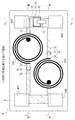
図2から図5は、本発明に係る集積型電子部品Xを表す。図2は、集積型電子部品Xの平面図である。図3から図5は、各々、図2の線III−III、線IV−IV、および線V−Vに沿った断面図である。 2 to 5 show an integrated electronic component X according to the present invention. FIG. 2 is a plan view of the integrated electronic component X. FIG. 3 to 5 are cross-sectional views taken along lines III-III, IV-IV, and VV in FIG. 2, respectively.
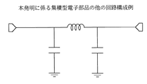
集積型電子部品Xは、基板Sと、多段コイルインダクタ10A,10Bと、キャパシタ20と、立体配線30と、パッド部40A,40B,40C,40Dとを備え、図6に示す回路構成を有する。
The integrated electronic component X includes a substrate S,
基板Sは、半導体基板、絶縁膜が表面に形成された半導体基板、石英基板、ガラス基板、圧電基板、セラミック基板、SOI(silicon on insulator)基板、SOQ(silicon on quartz)基板、またはSOG(silicon on glass)基板である。半導体基板は、例えば、単結晶シリコンなどのシリコン材料よりなる。圧電基板を構成する圧電材料としては、例えばLiTaO3、LiNbO3、AlN、ZnO、および圧電セラミックが挙げられる。 The substrate S is a semiconductor substrate, a semiconductor substrate with an insulating film formed on its surface, a quartz substrate, a glass substrate, a piezoelectric substrate, a ceramic substrate, an SOI (silicon on insulator) substrate, an SOQ (silicon on quartz) substrate, or an SOG (silicon on glass) substrate. The semiconductor substrate is made of, for example, a silicon material such as single crystal silicon. Examples of the piezoelectric material constituting the piezoelectric substrate include LiTaO 3 , LiNbO 3 , AlN, ZnO, and piezoelectric ceramic.
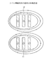
多段コイルインダクタ10A,10Bは、各々、本発明における受動部品に相当し、例えば図3および図4に表れているように、二段に配されたスパイラルコイル11,12と、これらを直列に接続する連絡部13とからなる。図2においては、多段コイルインダクタ10A,10Bを黒ベタ渦巻等で模式的に表す。図7は、多段コイルインダクタ10Aの分解平面図であり、図8は、多段コイルインダクタ10Bの分解平面図である。多段コイルインダクタ10A,10Bの各々において、スパイラルコイル11,12は、各々を流れる電流の方向が同一方向となるような巻形状を有する。多段コイルインダクタ10A,10Bの各々においては、隣り合うコイル導線は空隙を介して離隔している。スパイラルコイル11,12の厚さは好ましくは3μm以上である。また、本実施形態では、スパイラルコイル11は、スパイラルコイル12より基板Sに近く、基板Sから離隔している。スパイラルコイル11および基板Sの離隔距離は、例えば1〜100μmである。このような多段コイルインダクタ10A,10Bは、例えばCu、Au、Ag、またはAlよりなる。
Each of the
集積型電子部品Xにおいて基板S上に設けられた多段コイルインダクタ10A,10Bについては、図1に示すような集中定数等価回路で表すことができ、また、上記の式(1)でQ値を表すことができる。上述のように、図1および式(1)においては、Lはインダクタのインダクタンスであり、Riはインダクタの抵抗であり、Rsは基板の抵抗であり、Cはインダクタの寄生容量であり、ωは角振動数であって2πf(fは周波数)に等しい。
The
キャパシタ20は、本発明における受動部品に相当し、図5に示すように、第1電極21と、第2電極22と、これらの間の誘電体層23とからなる積層構造を有する。第1電極21は、基板S上に設けられ、第2電極22は、基板Sから離隔して基板Sに沿って設けられている。第2電極22の厚さは好ましくは3μm以上である。また、第1電極21は、例えば、所定の多層構造を有し、当該多層構造の各層には、Cu、Au、Ag、およびAlから選択される金属が含まれる。第2電極22は、例えばCu、Au、Ag、またはAlよりなる。誘電体層23は、例えば酸化シリコン、窒化シリコン、酸化アルミニウム、酸化タンタル、または酸化チタンよりなる。
The
立体配線30は、本発明において基板上の各コンポーネント(受動部品,パッド部)を電気的に接続するための配線であり、基板Sに接して延びる部位を有する第1配線部31と、基板Sから離隔して基板Sに沿って延びる第2配線部32と、これら第1配線部31および第2配線部32に接続する第3配線部33とからなる。図の明確化の観点より、図2においては、立体配線30のうち第1配線部31のみをハッチングを付して表す。立体配線30は、例えばCu、Au、Ag、またはAlよりなる。また、第1配線部31および第2配線部32の厚さは好ましくは3μm以上である。
The three-
パッド部40A〜40Dは、外部接続用の電気パッドである。図6から理解できるように、パッド部40A,40Bは、電気信号入出力用の端子としての機能するものであり、パッド部40C,40Dは、グラウンド接続されている。パッド部40A〜40Dは、例えば、Ni母体およびその上位表面を被覆するAu膜からなる。
The
図6に示すように、多段コイルインダクタ10Aは、パッド部40A,40Cおよびキャパシタ20の第1電極21と電気的に接続している。具体的には、図3に示すように、多段コイルインダクタ10Aの図中下位のスパイラルコイル11の端部11aは、第1配線部31を介して、パッド部40Aおよびキャパシタ20の第1電極21と電気的に接続し、且つ、多段コイルインダクタ10Aの図中上位のスパイラルコイル12の端部12aは、第2配線部32、第3配線部33、および第1配線部31を介して、パッド部40Cと電気的に接続している。
As shown in FIG. 6, the
図6に示すように、多段コイルインダクタ10Bは、パッド部40B,40Dおよびキャパシタ20の第2電極22と電気的に接続している。具体的には、図4および図5に示すように、多段コイルインダクタ10Bの図中上位のスパイラルコイル12の端部12aは、第2配線部32、第3配線部33、および第1配線部31を介して、パッド部40Bと電気的に接続し、更に第2配線部32を介してキャパシタ20の第2電極22と電気的に接続し、且つ、多段コイルインダクタ10Bの図中下位のスパイラルコイル11の端部11aは、第1配線部31を介してパッド部40Dと電気的に接続している。
As shown in FIG. 6, the
以上のような構成を有する集積型電子部品Xの多段コイルインダクタ10A,10Bの各々においては、交流電流通電時にスパイラルコイル11,12どうしの相互電磁誘導によって各スパイラルコイル11,12にて相互インダクタンスが生じるので、インダクタ全体について大きなインダクタンスLを得やすい。そのため、多段コイルインダクタ10A,10Bでは、インダクタを構成する導線について、所定のインダクタンスLを実現するのに要する全長は短い傾向にある。一方、多段コイルインダクタ10A,10Bの各々を構成する導線の全長が短いほど、多段コイルインダクタ10A,10Bの各抵抗Riは小さい傾向にある。したがって、多段コイルインダクタ10A,10Bは、小さな抵抗Riにて所定のインダクタンスLを実現するのに適しているのである。小さな抵抗Riにて所定のインダクタンスLを実現することは、上記の式(1)の特に1番目の因子に着目すると理解できるように、Q値の増大に資する。
In each of the
また、集積型電子部品Xの多段コイルインダクタ10A,10Bの各々においては、図9に示すように、スパイラルコイル11,12に対して同方向の交流電流を流すことにより、当該コイル間に形成される磁場強度を抑制することができる(スパイラルコイル11を流れる電流によりスパイラルコイル11周囲に形成される磁場と、スパイラルコイル12を流れる電流によりスパイラルコイル12周囲に形成される磁場とが、スパイラルコイル11,12間で打ち消し合うからである)。これにより、スパイラルコイル11,12のコイル導線における高周波電流の表皮効果を緩和することができ、従って、当該コイル導線の抵抗Ri(高周波抵抗)を低減することが可能である。上記の式(1)から理解できるように、抵抗Riの低減はQ値の増大に資する。
Further, in each of the
加えて、集積型電子部品Xの多段コイルインダクタ10A,10Bの各々においては、コイル導線は、有意な厚さのセラミック(大きな誘電率を有する)等に包囲されておらず、特に、隣り合うコイル導線間にはセラミック等は介在せず、従って、多段コイルインダクタ10A,10Bの各々は寄生容量Cを抑制するのに適している。上記の式(1)から理解できるように、寄生容量Cの抑制はQ値の増大に資する。
In addition, in each of the
このように集積型電子部品Xの多段コイルインダクタ10A,10Bは、高いQ値を実現するのに適している。したがって、このような多段コイルインダクタ10A,10Bを備える集積型電子部品Xは、高いQ値を実現するのに適しているのである。
Thus, the
また、集積型電子部品Xは、良好な高周波特性を実現するうえでも適している。一般に、インダクタの寄生容量が小さいほど、当該インダクタの自己共振周波数や当該インダクタのQ値がピークを示す周波数は高周波側にシフトし、当該インダクタについて良好な高周波特性を得られやすい。そのため、上述のように寄生容量Cを抑制するのに適している多段コイルインダクタ10A,10Bは、良好な高周波特性を実現するうえでも適している。したがって、このような多段コイルインダクタ10A,10Bを備える集積型電子部品Xは、良好な高周波特性を実現するうえで適しているのである。
The integrated electronic component X is also suitable for realizing good high frequency characteristics. In general, as the parasitic capacitance of an inductor is smaller, the self-resonant frequency of the inductor and the frequency at which the Q value of the inductor has a peak shift to the high frequency side, and it is easier to obtain good high frequency characteristics for the inductor. Therefore, the
加えて、集積型電子部品Xは、各コンポーネント(受動部品,パッド部)の間を、電気的に接続するための配線における損失を抑制するのに適している。集積型電子部品Xは、基板Sに接して延びる部位を有する第1配線部31と、基板Sから離隔して基板Sに沿って延びる第2配線部32と、これら第1配線部31および第2配線部32に接続する第3配線部33とを含む立体配線30を備えるところ、立体配線30は、これら3種類の配線部の適宜の組み合せにより、各コンポーネントの間を、自由度高く接続することが可能である。すなわち、集積型電子部品Xでは、基板S上の各コンポーネント間の配線設計における自由度が高いのである。配線設計の自由度が高いことは、各コンポーネント間の配線長の最短化を実現するうえで好適であり、配線どうしの交差および配線とコイル導線の交差を回避するうえで好適である。各コンポーネント間の配線長の最短化は、配線の高周波抵抗を抑制するのに資する。また、配線どうしの交差および配線とコイル導線の交差の回避は、当該交差構造に起因して電磁場相互誘導により配線やコイル導線に渦電流が生じてしまうのを抑制するのに、資する。これら、高周波抵抗の抑制および渦電流の抑制は、各コンポーネント間を接続するための配線における損失を抑制するのに適している。そして、配線損失の抑制は、集積型電子部品X全体において高いQ値を実現するのに好適なのである。
In addition, the integrated electronic component X is suitable for suppressing loss in wiring for electrically connecting each component (passive component, pad portion). The integrated electronic component X includes a
以上のように、集積型電子部品Xは、高いQ値および良好な高周波特性を実現するのに適している。 As described above, the integrated electronic component X is suitable for realizing a high Q value and good high-frequency characteristics.
また、本実施形態における多段コイルインダクタ10A,10Bは、多段配置されるスパイラルコイル11,12の数を増減するのに加え、各スパイラルコイル11,12にて同一平面内でのコイル巻数を増減することによっても、インダクタ全体のコイル巻数を増減することが可能であり、従って、効率よく所要のインダクタンスLを達成することができる。
The
加えて、本実施形態では、多段コイルインダクタ10A,10Bにおける、基板に最も近いスパイラルコイル11は、基板Sから離隔している。このような構成は、多段コイルインダクタ10A,10Bに通電することに起因して基板Sに生ずる誘導電流を抑制するのに好適である。
In addition, in this embodiment, the
図10から図15は、集積型電子部品Xの製造方法を表す。この方法は、バルクマイクロマシニング技術により集積型電子部品Xを製造するための一手法である。図10から図15においては、図15(c)に示す多段コイルインダクタ10、キャパシタ20、2つのパッド部40、および、立体配線30においてこれらに接続する箇所、の形成過程を、断面の変化で表す。当該断面は、加工が施される材料基板における単一の集積型電子部品形成区画に含まれる複数の所定箇所の断面を、モデル化して連続断面としたものである。多段コイルインダクタ10は、多段コイルインダクタ10A,10Bに相当する。パッド部40は、パッド部40A〜40Dに相当する。
10 to 15 show a method for manufacturing the integrated electronic component X. FIG. This method is one method for manufacturing the integrated electronic component X by bulk micromachining technology. 10 to 15, the formation process of the
集積型電子部品Xの製造においては、まず、図10(a)に示すように、キャパシタ20の第1電極21を基板S上に形成する。例えば、スパッタリング法により所定の金属材料を基板S上に成膜した後、所定のウェットエッチングまたはドライエッチングにより当該金属膜をパターニングすることによって、第1電極21を形成することができる。
In the manufacture of the integrated electronic component X, first, the
次に、図10(b)に示すように、キャパシタ20の誘電体層23を第1電極21上に形成する。例えば、スパッタリング法により所定の誘電体材料を少なくとも第1電極21上に成膜した後、所定のウェットエッチングまたはドライエッチングにより当該誘電体膜をパターニングすることによって、誘電体層23を形成することができる。
Next, as shown in FIG. 10B, the
次に、図10(c)に示すように、第1電極21および誘電体層23を覆うように、電気めっき用のシード層101(太線で表す)を基板S上に形成する。シード層101は、例えば、Ti膜およびその上のAu膜からなる積層構造、Cr膜およびその上のAu膜からなる積層構造、Ti膜およびその上のCu膜からなる積層構造、または、Cr膜およびその上のCu膜からなる積層構造を有する。シード層101の形成手法としては、例えば蒸着法やスパッタリング法を採用することができる。後出のシード層の構成および形成手法は、このシード層101と同様である。
Next, as shown in FIG. 10C, an electroplating seed layer 101 (represented by a thick line) is formed on the substrate S so as to cover the
次に、図10(d)に示すように、1段目肉厚導体部形成用のレジストパターン102を形成する。本方法では、1段目肉厚導体部とは、キャパシタ20の第2電極22および立体配線30の第1配線部31である。レジストパターン102は、第2電極22および第1配線部31のパターン形状に対応する開口部102aを有する。レジストパターン102の形成においては、まず、基板S上に、第1電極21および誘電体層23の上方から、液状のフォトレジストをスピンコーティングにより成膜する。次に、露光処理およびその後の現像処理を経て、当該フォトレジスト膜をパターニングする。フォトレジストとしては、例えば、AZP4210(AZエレクトロニックマテリアルズ製)やAZ1500(AZエレクトロニックマテリアルズ製)を使用することができる。後出のレジストパターンについても、このようなフォトレジストの成膜ならびにその後の露光処理および現象処理を経て、形成することができる。
Next, as shown in FIG. 10D, a resist
次に、図11(a)に示すように、電気めっき法により、レジストパターン102の開口部102aにて、1段目肉厚導体部(第2電極22,第1配線部31)を形成する。当該電気めっき時には、シード層101が通電される。
Next, as shown in FIG. 11A, the first thick conductor portion (
次に、図11(b)に示すように、例えば剥離液を作用させることにより、レジストパターン102を除去する。剥離液としては、例えばAZリムーバ700(AZエレクトロニックマテリアルズ製)を使用することができる。後出のレジストパターンの除去手法については、レジストパターン102の当該除去手法と同様である。
Next, as shown in FIG. 11B, the resist
次に、図11(c)に示すように、パッド部形成用のレジストパターン103を形成する。レジストパターン103は、各パッド部40のパターン形状に対応する開口部103aを有する。
Next, as shown in FIG. 11C, a resist
次に、図11(d)に示すように、電気めっき法により、レジストパターン103の開口部103aにてパッド部40を形成する。当該電気めっき時には、シード層101が通電される。パッド部40は、Ni母体およびその上位表面を被覆するAu膜からなるのが好ましい。
Next, as shown in FIG. 11D, a
次に、図12(a)に示すように、レジストパターン103を除去し、そして、当該除去の後にシード層101において露出している箇所を除去する(シード層101において露出していない箇所については、図12(a)以降の図で省略する)。シード層101は、例えばイオンミリング法によって除去することができる。後出のシード層の除去手法としても、イオンミリング法を採用することができる。
Next, as shown in FIG. 12A, the resist
次に、図12(b)に示すようにレジストパターン104を形成する。レジストパターン104は、1段目肉厚導体部の上位に2段目肉厚導体部を形成するための犠牲層として機能するものであり、1段目肉厚導体部のパターン形状に対応する開口部104aを有する。本方法では、2段目肉厚導体部とは、多段コイルインダクタ10のスパイラルコイル11、並びに、立体配線30の第2配線部32および第3配線部33である。レジストパターン104は、1段目肉厚導体部(第2電極22,第1配線部31)の一部が開口部104aにて露出するように、形成される。また、本実施形態ではレジストパターンにより構成される、本発明における犠牲層、の構成材料については、レジスト材料に代えて、パターニング可能であり且つ除去可能である他の材料を採用してもよい(後出の犠牲層についても同様である)。
Next, a resist
次に、図12(c)に示すように、レジストパターン104の表面、1段目肉厚導体部において開口部104aにて露出する表面、およびパッド部40の表面にわたり、シード層105(太線で表す)を形成する。
Next, as shown in FIG. 12C, the seed layer 105 (bold line) extends across the surface of the resist
次に、図12(d)に示すように、2段目肉厚導体部形成用のレジストパターン106を形成する。レジストパターン106は、多段コイルインダクタ10の、スパイラルコイル11および連絡部13の一部、並びに、立体配線30の、第2配線部32および第3配線部33の一部、のパターン形状に対応する開口部106aを有する。
Next, as shown in FIG. 12D, a resist
次に、図13(a)に示すように、電気めっき法により、レジストパターン106の開口部106aにて、2段目肉厚導体部(スパイラルコイル11,連絡部13の一部,第2配線部32,第3配線部33の一部)を形成する。当該電気めっき時には、シード層105が通電される。
Next, as shown in FIG. 13 (a), the second-stage thick conductor portion (
次に、図13(b)に示すように、レジストパターン106の上に、3段目肉厚導体部形成用のレジストパターン107を形成する。本方法では、3段目肉厚導体部とは、多段コイルインダクタ10の連絡部13の一部、および、立体配線30の第3配線部33の一部である。レジストパターン107は、連絡部13の一部および第3配線部33の一部のパターン形状に対応する開口部107aを有する。
Next, as shown in FIG. 13B, a resist
次に、図13(c)に示すように、電気めっき法により、レジストパターン107の開口部107aにて、3段目肉厚導体部(連絡部13の一部,第3配線部33の一部)を形成する。当該電気めっき時には、シード層105が通電される。
Next, as shown in FIG. 13C, the third-tier thick conductor portion (a part of the
次に、図13(d)に示すように、レジストパターン106,107を除去し、そして、当該除去の後にシード層105において露出している箇所を除去する(シード層105において露出していない箇所については、図13(d)以降の図で省略する)。この後、図14(a)に示すように、レジストパターン104を除去する。
Next, as shown in FIG. 13D, the resist
次に、図14(b)に示すようにレジストパターン108を形成する。レジストパターン108は、3段目肉厚導体部の上位に4段目肉厚導体部を形成するための犠牲層として機能するものであり、3段目肉厚導体部のパターン形状に対応する開口部108aを有する。本方法では、4段目肉厚導体部とは、多段コイルインダクタ10の、スパイラルコイル12および連絡部13の一部、並びに、立体配線30の第2配線部32である。また、レジストパターン108は、3段目肉厚導体部の一部が開口部108aにて露出するように、形成される。
Next, as shown in FIG. 14B, a resist
次に、図14(c)に示すように、レジストパターン108の表面、および、3段目肉厚導体部において開口部108aにて露出する表面にわたり、シード層109(太線で表す)を形成する。
Next, as shown in FIG. 14C, a seed layer 109 (represented by a thick line) is formed across the surface of the resist
次に、図14(d)に示すように、4段目肉厚導体部形成用のレジストパターン110を形成する。レジストパターン110は、多段コイルインダクタ10の、スパイラルコイル12および連絡部13の一部、並びに、立体配線30の第2配線部32、のパターン形状に対応する開口部110aを有する。
Next, as shown in FIG. 14D, a resist
次に、図15(a)に示すように、電気めっき法により、レジストパターン110の開口部110aにて、4段目肉厚導体部(スパイラルコイル12,連絡部13の一部,第2配線部32)を形成する。当該電気めっき時には、シード層109が通電される。
Next, as shown in FIG. 15A, the fourth-tier thick conductor portion (
次に、図15(b)に示すように、レジストパターン110を除去し、そして、当該除去の後にシード層109において露出している箇所を除去する(シード層109において露出していない箇所については、図15(b)以降の図で省略する)。この後、図15(c)に示すように、レジストパターン108を除去する。
Next, as shown in FIG. 15B, the resist
レジストパターン108の除去の後、好ましくは、多段コイルインダクタ10および/または立体配線30において露出している箇所を、耐食性膜および磁性体膜から選択される膜または当該膜を含む多層膜により被覆する。耐食性膜による被覆は、多段コイルインダクタのコイル導線や、立体配線の各配線部の、耐食性向上の観点から好適である。耐食性膜の構成材料としては、例えばAu,Rh,Ruなどの金属材料や、所定の誘電体材料が挙げられる。誘電体材料としては、例えば、BCB(Benzocyclobutenes)、PBO(Polybenzoxazoles)、ポリイミドなどの樹脂材料や、酸化シリコン、窒化シリコン、酸化アルミニウムなどが挙げられる。一方、磁性体膜による被覆は、特にコイル導線周囲の発生磁場を増大するのに好適である。コイル導線周囲の発生磁場の増大は、多段コイルインダクタのインダクタンスLを増大するうえで好適である。また、磁性体膜は、当該磁性体膜内で渦電流が発生してしまうのを抑制する観点から、高抵抗材料よりなるのが好ましい。このような磁性体膜の構成材料としては、例えば、Fe−Al−O系合金、CoFeB−SiO2系高抵抗磁性体などが挙げられる。
After removal of the resist
以上のようにして、多段コイルインダクタ10、キャパシタ20、立体配線30、およびパッド部40を基板S上に形成し、集積型電子部品Xを製造することができる。
As described above, the integrated electronic component X can be manufactured by forming the
集積型電子部品Xの多段コイルインダクタ10A,10Bについては、図16および図17に示すように、基板Sに接して設けてもよい(第1変形例)。この場合、立体配線30については、多段コイルインダクタ10A,10Bの各々のスパイラルコイル11,12の高さ位置に応じて、上述の実施形態とは異なる寸法や形状を採用してもよい。
The
また、集積型電子部品Xについては、図18および図19に示すように、多段コイルインダクタ10A,10Bを基板Sに接して設けたうえで、封止材50により部分的に封止してもよい(第2変形例)。封止材50は、例えば、BCB、PBO、ポリイミドなどの樹脂材料よりなる。相対的に上位に位置する導体部(例えばスパイラルコイル12や第2配線部32)を形成した後に、相対的に下位に位置する導体部(例えばスパイラルコイル11や第1配線部11)を上述の耐食性膜により被覆することは、困難な場合がある。本変形例では、相対的に下位に位置する導体部は、封止材50により覆われて耐食性が確保され得るため、相対的に上位に位置する導体部を形成した後に、相対的に下位に位置する導体部を耐食性膜により被覆する必要はない。
As for the integrated electronic component X, as shown in FIGS. 18 and 19, the
図20から図23は、上述の第1変形例の第1の製造方法を表す。この方法は、バルクマイクロマシニング技術により当該第1変形例を製造するための一手法である。図20から図23においては、図23(d)に示す多段コイルインダクタ10、キャパシタ20、2つのパッド部40、および、立体配線30においてこれらに接続する箇所、の形成過程を、断面の変化で表す。当該断面は、加工が施される材料基板における単一の集積型電子部品形成区画に含まれる複数の所定箇所の断面を、モデル化して連続断面としたものである。多段コイルインダクタ10は、多段コイルインダクタ10A,10Bに相当する。パッド部40は、パッド部40A〜40Dに相当する。
20 to 23 show a first manufacturing method of the first modification described above. This method is one method for manufacturing the first modified example by the bulk micromachining technique. 20 to 23, the formation process of the
本方法においては、まず、図20(a)に示すように、キャパシタ20の第1電極21を基板S上に形成する。次に、図20(b)に示すように、キャパシタ20の誘電体層23を第1電極21上に形成する。次に、図20(c)に示すように、第1電極21および誘電体層23を覆うように、電気めっき用のシード層101を基板S上に形成する。これらの工程は、具体的には、図10の(a)〜(c)を参照して上述したのと同様である。
In this method, first, the
次に、図20(d)に示すように、1段目肉厚導体部形成用のレジストパターン201を形成する。本方法では、1段目肉厚導体部とは、多段コイルインダクタ10の、スパイラルコイル11および連絡部13の一部、キャパシタ20の第2電極22、並びに、立体配線30の第1配線部31である。レジストパターン201は、スパイラルコイル11、連絡部13の一部、第2電極22、および第1配線部31のパターン形状に対応する開口部201aを有する。
Next, as shown in FIG. 20D, a resist
次に、図20(e)に示すように、電気めっき法により、レジストパターン201の開口部201aにて、1段目肉厚導体部(スパイラルコイル11,連絡部13の一部,第2電極22,第1配線部31)を形成する。当該電気めっき時には、シード層101が通電される。
Next, as shown in FIG. 20 (e), by the electroplating method, the first thick conductor portion (
次に、図21(a)に示すように、レジストパターン201の上位に、2段目肉厚導体部形成用のレジストパターン202を形成する。本方法では、2段目肉厚導体部とは、多段コイルインダクタ10の連絡部13の一部、および、立体配線30の第3配線部33である。レジストパターン202は、連絡部13の一部および第3配線部33のパターン形状に対応する開口部202aを有する。
Next, as shown in FIG. 21A, a resist
次に、図21(b)に示すように、電気めっき法により、レジストパターン202の開口部202aにて、2段目肉厚導体部(連絡部13の一部,第3配線部33)を形成する。当該電気めっき時には、シード層101が通電される。この後、図21(c)に示すように、レジストパターン201,202を除去する。
Next, as shown in FIG. 21B, the second-tier thick conductor portion (a part of the connecting
次に、図21(d)に示すように、パッド部形成用のレジストパターン203を形成する。レジストパターン203は、各パッド部40のパターン形状に対応する開口部203aを有する。
Next, as shown in FIG. 21D, a resist
次に、図22(a)に示すように、電気めっき法により、レジストパターン203の開口部203aにてパッド部40を形成する。当該電気めっき時には、シード層101が通電される。パッド部40は、Ni母体およびその上位表面を被覆するAu膜からなるのが好ましい。この後、図22(b)に示すように、レジストパターン203を除去し、そして、当該除去の後にシード層101において露出している箇所を除去する(シード層101において露出していない箇所については、図22(b)以降の図で省略する)。
Next, as shown in FIG. 22A, a
次に、図22(c)に示すようにレジストパターン204を形成する。レジストパターン204は、2段目肉厚導体部の上位に3段目肉厚導体部を形成するための犠牲層として機能するものであり、2段目肉厚導体部のパターン形状に対応する開口部204aを有する。本方法では、3段目肉厚導体部とは、多段コイルインダクタ10の、スパイラルコイル12および連絡部13の一部、並びに、立体配線30の第2配線部32である。また、レジストパターン204は、2段目肉厚導体部の一部が開口部204aにて露出するように、形成される。
Next, a resist
次に、図22(d)に示すように、レジストパターン204の表面、および、2段目肉厚導体部において開口部204aにて露出する表面にわたり、シード層205(太線で表す)を形成する。
Next, as shown in FIG. 22D, a seed layer 205 (represented by a thick line) is formed over the surface of the resist
次に、図23(a)に示すように、3段目肉厚導体部形成用のレジストパターン206を形成する。レジストパターン206は、多段コイルインダクタ10の、スパイラルコイル12および連絡部13の一部、並びに、立体配線30の第2配線部32、のパターン形状に対応する開口部206aを有する。
Next, as shown in FIG. 23A, a resist
次に、図23(b)に示すように、電気めっき法により、レジストパターン206の開口部206aにて、3段目肉厚導体部(スパイラルコイル12,連絡部13の一部,第2配線部32)を形成する。当該電気めっき時には、シード層205が通電される。
Next, as shown in FIG. 23 (b), the third-tier thick conductor portion (
次に、図23(c)に示すように、レジストパターン206を除去し、そして、当該除去の後にシード層205において露出している箇所を除去する(シード層205において露出していない箇所については、図23(c)以降の図で省略する)。
Next, as shown in FIG. 23C, the resist
次に、図23(d)に示すように、レジストパターン204を除去する。レジストパターン204の除去の後、好ましくは、多段コイルインダクタ10および/または立体配線30において露出している箇所を、耐食性膜および磁性体膜から選択される膜または当該膜を含む多層膜により被覆する。以上のようにして、多段コイルインダクタ10、キャパシタ20、立体配線30、およびパッド部40を基板S上に形成し、上述の第1変形例を製造することができる。
Next, as shown in FIG. 23D, the resist
図24から図27は、上述の第1変形例の第2の製造方法を表す。この方法は、バルクマイクロマシニング技術により当該第1変形例を製造するための一手法である。図24から図27においては、図27(c)に示す多段コイルインダクタ10、キャパシタ20、2つのパッド部40、および、立体配線30においてこれらに接続する箇所、の形成過程を、断面の変化で表す。当該断面は、加工が施される材料基板における単一の集積型電子部品形成区画に含まれる複数の所定箇所の断面を、モデル化して連続断面としたものである。多段コイルインダクタ10は、多段コイルインダクタ10A,10Bに相当する。パッド部40は、パッド部40A〜40Dに相当する。
24 to 27 show a second manufacturing method of the first modification described above. This method is one method for manufacturing the first modified example by the bulk micromachining technique. 24 to 27, the formation process of the
本方法においては、まず、図24(a)に示すように、キャパシタ20の第1電極21を基板S上に形成する。次に、図24(b)に示すように、キャパシタ20の誘電体層23を第1電極21上に形成する。次に、図24(c)に示すように、第1電極21および誘電体層23を覆うように、電気めっき用のシード層101を基板S上に形成する。これらの工程について具体的には、図10の(a)〜(c)を参照して上述したのと同様である。
In this method, first, the
次に、図24(d)に示すように、1段目肉厚導体部形成用のレジストパターン301を形成する。本方法では、1段目肉厚導体部とは、多段コイルインダクタ10のスパイラルコイル11および連絡部13の一部、キャパシタ20の第2電極22、並びに、立体配線30の第1配線部31である。レジストパターン301は、スパイラルコイル11、連絡部13の一部、第2電極22、および第1配線部31のパターン形状に対応する開口部301aを有する。
Next, as shown in FIG. 24D, a resist
次に、図25(a)に示すように、電気めっき法により、レジストパターン301の開口部301aにて、1段目肉厚導体部(スパイラルコイル11,連絡部13の一部,第2電極22,第1配線部31)を形成する。当該電気めっき時には、シード層101が通電される。この後、図25(b)に示すように、例えば剥離液を作用させることにより、レジストパターン301を除去する。
Next, as shown in FIG. 25 (a), the first-tier thick conductor portion (
次に、図25(c)に示すように、パッド部形成用のレジストパターン302を形成する。レジストパターン302は、各パッド部40のパターン形状に対応する開口部302aを有する。
Next, as shown in FIG. 25C, a pad portion forming resist
次に、図25(d)に示すように、電気めっき法により、レジストパターン302の開口部302aにてパッド部40を形成する。当該電気めっき時には、シード層101が通電される。パッド部40は、Ni母体およびその上位表面を被覆するAu膜からなるのが好ましい。この後、図26(a)に示すように、レジストパターン302を除去し、そして、当該除去の後にシード層101において露出している箇所を除去する(シード層101において露出していない箇所については、図26(a)以降の図で省略する)。
Next, as shown in FIG. 25D, the
次に、図26(b)に示すように、2段目肉厚導体部形成用のレジストパターン303を形成する。本方法では、2段目肉厚導体部とは、多段コイルインダクタ10の連絡部13の一部および立体配線30の第3配線部33である。レジストパターン303は、連絡部13の一部および第3配線部33のパターン形状に対応する開口部303aを有し、1段目肉厚導体部の一部が開口部303aにて露出するように、形成される。また、レジストパターン303は、2段目肉厚導体部の上位に3段目肉厚導体部を形成するための犠牲層としても機能するものである。本方法では、3段目肉厚導体部とは、多段コイルインダクタ10の、スパイラルコイル12および連絡部13の一部、並びに、立体配線30の第2配線部32である。
Next, as shown in FIG. 26B, a resist
次に、図26(c)に示すように、レジストパターン303の表面、および、1段目肉厚導体部において開口部303aにて露出する表面にわたり、シード層304(太線で表す)を形成する。
Next, as shown in FIG. 26C, a seed layer 304 (represented by a thick line) is formed over the surface of the resist
次に、図26(d)に示すように、3段目肉厚導体部形成用のレジストパターン305を形成する。レジストパターン305は、多段コイルインダクタ10の、スパイラルコイル12および連絡部13の一部、並びに、立体配線30の第2配線部32、のパターン形状に対応する開口部305aを有する。
Next, as shown in FIG. 26D, a resist
次に、図27(a)に示すように、電気めっき法により、レジストパターン303の開口部303aにて2段目肉厚導体部(連絡部13の一部,第3配線部33)を形成し、レジストパターン305の開口部305aにて、3段目肉厚導体部(スパイラルコイル12,連絡部13の一部,第2配線部32)を形成する。当該電気めっき時には、シード層304が通電される。
Next, as shown in FIG. 27A, a second-tier thick conductor portion (a part of the connecting
次に、図27(b)に示すように、レジストパターン305を除去し、そして、当該除去の後にシード層304において露出している箇所を除去する(シード層304において露出していない箇所については、図27(b)以降の図で省略する)。
Next, as shown in FIG. 27B, the resist
次に、図27(c)に示すように、レジストパターン303を除去する。レジストパターン303の除去の後、好ましくは、多段コイルインダクタ10および/または立体配線30において露出している箇所を、耐食性膜および磁性体膜から選択される膜または当該膜を含む多層膜により被覆する。以上のようにして、多段コイルインダクタ10、キャパシタ20、立体配線30、およびパッド部40を基板S上に形成し、上述の第1変形例を製造することができる。
Next, as shown in FIG. 27C, the resist
図28から図32は、上述の第2変形例の製造方法を表す。この方法は、バルクマイクロマシニング技術により当該第2変形例を製造するための一手法である。図28から図32においては、図32(d)に示す多段コイルインダクタ10、キャパシタ20、2つのパッド部40、および、立体配線30においてこれらに接続する箇所、の形成過程を、断面の変化で表す。当該断面は、加工が施される材料基板における単一の集積型電子部品形成区画に含まれる複数の所定箇所の断面を、モデル化して連続断面としたものである。多段コイルインダクタ10は、多段コイルインダクタ10A,10Bに相当する。パッド部40は、パッド部40A〜40Dに相当する。
FIG. 28 to FIG. 32 show the manufacturing method of the second modified example described above. This method is one method for manufacturing the second modified example by a bulk micromachining technique. 28 to 32, the formation process of the
本方法においては、まず、図28(a)に示すように、キャパシタ20の第1電極21を基板S上に形成する。次に、図28(b)に示すように、キャパシタ20の誘電体層23を第1電極21上に形成する。次に、図28(c)に示すように、第1電極21および誘電体層23を覆うように、電気めっき用のシード層101を基板S上に形成する。これらの工程について具体的には、図10の(a)〜(c)を参照して上述したのと同様である。
In this method, first, the
次に、図28(d)に示すように、1段目肉厚導体部形成用のレジストパターン401を形成する。本方法では、1段目肉厚導体部とは、多段コイルインダクタ10の、スパイラルコイル11および連絡部13の一部、キャパシタ20の第2電極22、並びに、立体配線30の第1配線部31である。レジストパターン401は、スパイラルコイル11、連絡部13の一部、第2電極22、および第1配線部31のパターン形状に対応する開口部401aを有する。
Next, as shown in FIG. 28D, a resist
次に、図29(a)に示すように、電気めっき法により、レジストパターン401の開口部401aにて、1段目肉厚導体部(スパイラルコイル11,連絡部13の一部,第2電極22,第1配線部31)を形成する。当該電気めっき時には、シード層101が通電される。この後、図29(b)に示すように、レジストパターン401を除去し、そして、シード層101において露出している箇所を除去する(シード層101において露出していない箇所については、図29(b)以降の図で省略する)。
Next, as shown in FIG. 29 (a), the first thick conductor portion (
次に、図29(c)に示すように誘電体膜402を形成する。誘電体膜402は所定の開口部402aを有する。誘電体膜402の形成においては、スピンコーティング法やスプレー法などにより所定の誘電体材料を成膜した後、当該膜をパターニングする。
Next, a
次に、図29(d)に示すように、誘電体膜402の表面、および、1段目肉厚導体部において開口部402aにて露出する表面にわたり、シード層403(太線で表す)を形成する。
Next, as shown in FIG. 29D, a seed layer 403 (represented by a thick line) is formed over the surface of the
次に、図30(a)に示すように、2段目肉厚導体部形成用のレジストパターン404を形成する。本方法では、2段目肉厚導体部とは、多段コイルインダクタ10の連絡部13の一部および立体配線30の第3配線部33である。レジストパターン404は、多段コイルインダクタ10の連絡部13の一部および立体配線30の第3配線部33のパターン形状に対応する開口部404aを有する。
Next, as shown in FIG. 30A, a resist
次に、図30(b)に示すように、電気めっき法により、レジストパターン404の開口部404aにて、2段目肉厚導体部(連絡部13の一部,第3配線部33)を形成する。当該電気めっき時には、シード層403が通電される。この後、図30(c)に示すように、レジストパターン404を除去する。
Next, as shown in FIG. 30B, the second-tier thick conductor portion (a part of the connecting
次に、図30(d)に示すように、パッド部形成用のレジストパターン405を形成する。レジストパターン405は、各パッド部40のパターン形状に対応する開口部405aを有する。
Next, as shown in FIG. 30D, a resist
次に、図31(a)に示すように、電気めっき法により、レジストパターン405の開口部405aにてパッド部40を形成する。当該電気めっき時には、シード層403が通電される。パッド部40は、Ni母体およびその上位表面を被覆するAu膜からなるのが好ましい。この後、図31(b)に示すように、レジストパターン405を除去し、そして、当該除去の後にシード層403において露出している箇所を除去する(シード層403において露出していない箇所については、図31(b)以降の図で省略する)。
Next, as shown in FIG. 31A, the
次に、図31(c)に示すようにレジストパターン406を形成する。レジストパターン406は、2段目肉厚導体部の上位に3段目肉厚導体部を形成するための犠牲層として機能するものであり、2段目肉厚導体部のパターン形状に対応する開口部406aを有する。本方法では、3段目肉厚導体部とは、多段コイルインダクタ10の、スパイラルコイル12および連絡部13の一部、並びに、立体配線30の第2配線部32である。また、レジストパターン406は、2段目肉厚導体部の一部が開口部406aにて露出するように、形成される。
Next, a resist
次に、図31(d)に示すように、レジストパターン406の表面、および、2段目肉厚導体部において開口部406aにて露出する表面にわたり、シード層407(太線で表す)を形成する。
Next, as shown in FIG. 31D, a seed layer 407 (represented by a thick line) is formed over the surface of the resist
次に、図32(a)に示すように、3段目肉厚導体部形成用のレジストパターン408を形成する。レジストパターン408は、多段コイルインダクタ10の、スパイラルコイル12および連絡部13の一部、並びに、立体配線30の第2配線部32、のパターン形状に対応する開口部408aを有する。
Next, as shown in FIG. 32A, a resist
次に、図32(b)に示すように、電気めっき法により、レジストパターン408の開口部408aにて、3段目肉厚導体部(スパイラルコイル12,連絡部13の一部,第2配線部32)を形成する。当該電気めっき時には、シード層407が通電される。
Next, as shown in FIG. 32 (b), the third-tier thick conductor portion (
次に、図32(c)に示すように、レジストパターン408を除去し、そして、当該除去の後にシード層407において露出している箇所を除去する(シード層407において露出していない箇所については、図32(c)以降の図で省略する)。
Next, as shown in FIG. 32C, the resist
次に、図32(d)に示すように、レジストパターン406を除去する。レジストパターン406の除去の後、好ましくは、多段コイルインダクタ10および/または立体配線30において露出している箇所を、耐食性膜および磁性体膜から選択される膜または当該膜を含む多層膜により被覆する。以上のようにして、多段コイルインダクタ10、キャパシタ20、立体配線30、パッド部40、および封止材50を基板S上に形成し、上述の第2変形例を製造することができる。
Next, as shown in FIG. 32D, the resist
集積型電子部品Xにおいては、図33に示すように、基板Sに凹部Saを設け、この凹部Sa上に多段コイルインダクタ10を設けてもよい(第3変形例)。このような構成は、集積型電子部品Xを小型化するうえで好適である。
In the integrated electronic component X, as shown in FIG. 33, the substrate S may be provided with a recess Sa, and the
本発明に係る集積型電子部品においては、上述のような多段コイルインダクタ10やキャパシタ20に代えて又は加えて、所定の抵抗や、フィルタを設けてもよい。フィルタとしては、例えば、LCRフィルタ、SAWフィルタ、FBARフィルタ、または機械共振を利用したフィルタを採用することができる。機械共振を利用したフィルタとしては、例えば、マイクロメカニカル ディスク レゾネータ、マイクロメカニカル リング レゾネータ、およびマイクロメカニカル ビーム レゾネータが挙げられる。
In the integrated electronic component according to the present invention, a predetermined resistor or a filter may be provided instead of or in addition to the
本発明に係る集積型電子部品においては、多段コイルインダクタ10、キャパシタ20、およびパッド部40の個数および基板S上の配置、並びに、立体配線30の形状を、適宜変更することにより、図6に示す回路構成に代えて、図34に示す回路構成や、図35に示す回路構成を実現することもできる。また、本発明に係る集積型電子部品においては、図6、図34、図35に示す回路構成を適宜組み合わせた、より複雑な回路構成を、実現することもできる。
In the integrated electronic component according to the present invention, the number of
本発明の集積型電子部品においては、上述のような多段コイルインダクタ10に代えて、ソレノイドコイルやトロイダルの形態の多段コイルインダクタを採用してもよい。また、本発明の集積型電子部品においては、基板上の構造全体を覆う封止樹脂を設けてもよい。この場合、封止樹脂は、多段コイルインダクタにおける隣り合うコイル導線の間に入り込む部位を有してもよい。封止樹脂を具備する構成は、集積型電子部品において高い信頼性を確保するうえで好適である。
In the integrated electronic component of the present invention, a multi-stage coil inductor in the form of a solenoid coil or a toroid may be employed instead of the
以上のまとめとして、本発明の構成およびそのバリエーションを以下に付記として列挙する。 As a summary of the above, the configurations of the present invention and variations thereof are listed below as supplementary notes.
(付記1)基板と、
複数の受動部品と、
外部接続用の複数のパッド部と、
立体配線と、を備え、
前記複数の受動部品は、前記基板上に設けられた多段コイルインダクタを含み、当該多段コイルインダクタは、多段配置された複数のコイルを有し、且つ、隣り合うコイル導線が空隙を介して離隔し、
前記立体配線は、前記基板に接して延びる第1配線部と、前記基板から離隔して当該基板に沿って延びる第2配線部と、当該第1および第2配線部に接続する第3配線部と、を含む、集積型電子部品。
(付記2)前記多段コイルインダクタは、空隙を介して互いに離隔する複数のスパイラルコイルを有する、付記1に記載の集積型電子部品。
(付記3)前記多段コイルインダクタはソレノイドコイルまたはトロイダルコイルである、付記1に記載の集積型電子部品。
(付記4)前記基板は、半導体基板、絶縁膜が表面に形成された半導体基板、石英基板、ガラス基板、圧電基板、セラミック基板、SOI基板、SOQ基板、またはSOG基板である、付記1から3のいずれか一つに記載の集積型電子部品。
(付記5)前記複数の受動部品は、キャパシタおよび/または抵抗を含む、付記1から4のいずれか一つに記載の集積型電子部品。
(付記6)前記キャパシタは、相対向する第1電極および第2電極を有し、前記第1電極は、前記基板上に設けられ、前記第2電極は、前記基板から離隔して前記基板に沿って設けられている、付記5に記載の集積型電子部品。
(付記7)前記多段コイルインダクタにおける、前記基板に最も近いコイルは、前記基板から離隔している、付記1から6のいずれか一つに記載の集積型電子部品。
(付記8)前記多段コイルインダクタにおける、前記基板に最も近いコイルは、前記基板上にパターン形成されている、付記1から6のいずれか一つに記載の集積型電子部品。
(付記9)前記複数の受動部品は、LCRフィルタ、SAWフィルタ、FBARフィルタ、および機械共振を利用したフィルタからなる群より選択されるフィルタを含む、付記1から8のいずれか一つに記載の集積型電子部品。
(付記10)前記複数の受動部品および前記立体配線を前記基板上にて封止するための封止樹脂を更に備える、付記1から9のいずれか一つに記載の集積型電子部品。
(付記11)前記封止樹脂は、前記多段コイルインダクタにおける隣り合うコイル導線の間に入り込む部位を有する、付記10に記載の集積型電子部品。
(付記12)前記多段コイルインダクタおよび/または前記立体配線は、耐食性膜および磁性体膜から選択される膜または当該膜を含む多層膜により被覆されている部位を有する、付記1から11のいずれか一つに記載の集積型電子部品。
(付記13)前記基板は凹部を有し、前記多段コイルインダクタは当該凹部に設けられている、付記1から12のいずれか一つに記載の集積型電子部品。
(付記14)電気めっき法により下位導体部を形成する工程と、
前記下位導体部の上位に上位導体部を形成するための、開口部を有する第1レジストパターンを、前記下位導体部の一部が前記開口部にて露出するように、形成する工程と、
前記第1レジストパターンの表面、および、前記下位導体部において前記開口部にて露出する表面にわたり、シード層を形成する工程と、
開口部を有する第2レジストパターンを第1レジストパターンの上位に形成する工程と、
電気めっき法により、前記第2レジストパターンの前記開口部にて上位導体部を形成する工程と、
前記第2レジストパターンを除去する工程と、
前記シード層を除去する工程と、
前記第1レジストパターンを除去する工程と、を含む、集積型電子部品製造方法。
(Appendix 1) a substrate;
Multiple passive components,
A plurality of pads for external connection;
Three-dimensional wiring,
The plurality of passive components include a multi-stage coil inductor provided on the substrate, the multi-stage coil inductor has a plurality of coils arranged in multiple stages, and adjacent coil conductors are separated via a gap. ,
The three-dimensional wiring includes a first wiring portion that extends in contact with the substrate, a second wiring portion that extends along the substrate and is spaced apart from the substrate, and a third wiring portion that is connected to the first and second wiring portions. And integrated electronic components.
(Additional remark 2) The said multistage coil inductor is an integrated electronic component of Additional remark 1 which has several spiral coils spaced apart from each other via the space | gap.
(Supplementary note 3) The integrated electronic component according to supplementary note 1, wherein the multistage coil inductor is a solenoid coil or a toroidal coil.
(Additional remark 4) The said board | substrate is a semiconductor substrate, the semiconductor substrate in which the insulating film was formed in the surface, a quartz substrate, a glass substrate, a piezoelectric substrate, a ceramic substrate, a SOI substrate, a SOQ substrate, or a SOG substrate, Additional remarks 1-3 The integrated electronic component according to any one of the above.
(Supplementary note 5) The integrated electronic component according to any one of supplementary notes 1 to 4, wherein the plurality of passive components include capacitors and / or resistors.
(Supplementary Note 6) The capacitor includes a first electrode and a second electrode facing each other, the first electrode is provided on the substrate, and the second electrode is spaced apart from the substrate and disposed on the substrate. The integrated electronic component according to appendix 5, provided along the line.
(Supplementary note 7) The integrated electronic component according to any one of supplementary notes 1 to 6, wherein the coil closest to the substrate in the multistage coil inductor is spaced apart from the substrate.
(Supplementary note 8) The integrated electronic component according to any one of supplementary notes 1 to 6, wherein the coil closest to the substrate in the multistage coil inductor is patterned on the substrate.
(Supplementary note 9) The plurality of passive components according to any one of supplementary notes 1 to 8, including a filter selected from the group consisting of an LCR filter, a SAW filter, an FBAR filter, and a filter using mechanical resonance. Integrated electronic components.
(Supplementary note 10) The integrated electronic component according to any one of supplementary notes 1 to 9, further comprising a sealing resin for sealing the plurality of passive components and the three-dimensional wiring on the substrate.
(Additional remark 11) The said sealing resin is an integrated electronic component of
(Supplementary note 12) Any one of Supplementary notes 1 to 11, wherein the multi-stage coil inductor and / or the three-dimensional wiring has a portion covered with a film selected from a corrosion-resistant film and a magnetic film or a multilayer film including the film. The integrated electronic component according to one.
(Supplementary note 13) The integrated electronic component according to any one of Supplementary notes 1 to 12, wherein the substrate has a concave portion, and the multi-stage coil inductor is provided in the concave portion.
(Appendix 14) A step of forming the lower conductor portion by electroplating,
Forming a first resist pattern having an opening for forming an upper conductor part above the lower conductor part so that a part of the lower conductor part is exposed at the opening;
Forming a seed layer over the surface of the first resist pattern and the surface exposed at the opening in the lower conductor portion;
Forming a second resist pattern having an opening above the first resist pattern;
Forming an upper conductor portion at the opening of the second resist pattern by electroplating;
Removing the second resist pattern;
Removing the seed layer;
And a step of removing the first resist pattern.
X 集積型電子部品
S 基板
10,10A,10B 多段コイルインダクタ
11,12 スパイラルコイル
13 連絡部
20 キャパシタ
21 第1電極
22 第2電極
23 誘電体層
30 立体配線
31 第1配線部
32 第2配線部
33 第3配線部
40,40A,40B,40C,40D パッド部
50 封止材
X Integrated Electronic
Claims (8)
前記基板上に設けられ、隣り合うコイル導線が空隙を介して離隔した第1段のコイルとその上に設けられた第2段のコイルとを含むインダクタと、
前記基板の表面に接した2つの第1配線部と、前記2つの第1配線部のうち、一方の第1配線部と接続し、前記基板から離隔して当該基板に沿って延びる第2配線部と、前記一方の第1配線部および前記第2配線部を接続し、前記基板の前記表面と交差する方向に延びる第3配線部とを有し、
前記第1段のコイルおよび前記第2段のコイルは前記基板と垂直な方向で重なっており、
前記第1段のコイルの一端が前記他方の第1配線部と直接に接続され他端が前記基板の前記表面と交差する方向に延びる連結部により前記第2段のコイルの一端に接続され、前記第2段のコイルの他端が前記第2配線部に接続されている、集積型電子部品。 A substrate,
An inductor including a first stage coil provided on the substrate and adjacent coil conductors separated by a gap and a second stage coil provided thereon;
Two first wiring portions that are in contact with the surface of the substrate, and a second wiring that is connected to one of the two first wiring portions and extends along the substrate at a distance from the substrate and parts, the connecting the first wiring portion and the second wiring portion of one, and a third wiring portion Ru extending in a direction crossing the surface of said substrate,
The first stage coil and the second stage coil overlap in a direction perpendicular to the substrate;
One end of the first stage of the coil is connected to one end of the second stage of the coil by a connecting portion to which the other end is directly connected to the first wiring portion of the other extends in a direction crossing the surface of said substrate, An integrated electronic component in which the other end of the second stage coil is connected to the second wiring portion.
Priority Applications (6)
| Application Number | Priority Date | Filing Date | Title |
|---|---|---|---|
| JP2005252596A JP4707056B2 (en) | 2005-08-31 | 2005-08-31 | Integrated electronic component and integrated electronic component manufacturing method |
| EP06254301.2A EP1760731B1 (en) | 2005-08-31 | 2006-08-16 | Integrated electronic device |
| KR1020060079679A KR100730672B1 (en) | 2005-08-31 | 2006-08-23 | Integrated electronic component, and method of manufacturing integrated electronic component |
| US11/509,577 US7948056B2 (en) | 2005-08-31 | 2006-08-25 | Integrated electronic device and method of making the same |
| CN2006101288079A CN1925321B (en) | 2005-08-31 | 2006-08-30 | Integrated electronic device and method of making the same |
| US13/064,347 US8518789B2 (en) | 2005-08-31 | 2011-03-21 | Integrated electronic device and method of making the same |
Applications Claiming Priority (1)
| Application Number | Priority Date | Filing Date | Title |
|---|---|---|---|
| JP2005252596A JP4707056B2 (en) | 2005-08-31 | 2005-08-31 | Integrated electronic component and integrated electronic component manufacturing method |
Related Child Applications (1)
| Application Number | Title | Priority Date | Filing Date |
|---|---|---|---|
| JP2008137019A Division JP4795385B2 (en) | 2008-05-26 | 2008-05-26 | Integrated electronic components |
Publications (3)
| Publication Number | Publication Date |
|---|---|
| JP2007067236A JP2007067236A (en) | 2007-03-15 |
| JP2007067236A5 JP2007067236A5 (en) | 2008-07-10 |
| JP4707056B2 true JP4707056B2 (en) | 2011-06-22 |
Family
ID=37401147
Family Applications (1)
| Application Number | Title | Priority Date | Filing Date |
|---|---|---|---|
| JP2005252596A Active JP4707056B2 (en) | 2005-08-31 | 2005-08-31 | Integrated electronic component and integrated electronic component manufacturing method |
Country Status (5)
| Country | Link |
|---|---|
| US (2) | US7948056B2 (en) |
| EP (1) | EP1760731B1 (en) |
| JP (1) | JP4707056B2 (en) |
| KR (1) | KR100730672B1 (en) |
| CN (1) | CN1925321B (en) |
Families Citing this family (73)
| Publication number | Priority date | Publication date | Assignee | Title |
|---|---|---|---|---|
| JP4842052B2 (en) | 2006-08-28 | 2011-12-21 | 富士通株式会社 | Inductor element and integrated electronic component |
| CN101730918B (en) | 2007-05-08 | 2013-03-27 | 斯卡尼梅特里科斯有限公司 | Ultra high speed signal transmission/reception |
| JP5090117B2 (en) * | 2007-09-28 | 2012-12-05 | 太陽誘電株式会社 | Electronic components |
| JP2009088161A (en) * | 2007-09-28 | 2009-04-23 | Fujitsu Media Device Kk | Electronic component |
| JP5090118B2 (en) * | 2007-09-28 | 2012-12-05 | 太陽誘電株式会社 | Electronic components |
| TWI397930B (en) * | 2007-11-06 | 2013-06-01 | Via Tech Inc | Spiral inductor |
| JP5172287B2 (en) * | 2007-11-19 | 2013-03-27 | 株式会社東芝 | Integrated circuit device |
| JP5058770B2 (en) * | 2007-12-12 | 2012-10-24 | 太陽誘電株式会社 | Electronic components |
| KR100922551B1 (en) * | 2007-12-26 | 2009-10-21 | 주식회사 동부하이텍 | Semiconductor device and method of manufacturing the same |
| JP5133047B2 (en) | 2007-12-28 | 2013-01-30 | 太陽誘電株式会社 | Manufacturing method of electronic parts |
| JP5154262B2 (en) * | 2008-02-26 | 2013-02-27 | 太陽誘電株式会社 | Electronic components |
| JP5133091B2 (en) | 2008-02-28 | 2013-01-30 | 太陽誘電株式会社 | Electronic component and manufacturing method thereof |
| US20090236689A1 (en) * | 2008-03-24 | 2009-09-24 | Freescale Semiconductor, Inc. | Integrated passive device and method with low cost substrate |
| JP4656196B2 (en) | 2008-07-11 | 2011-03-23 | 株式会社村田製作所 | Inductors and filters |
| US9599591B2 (en) | 2009-03-06 | 2017-03-21 | California Institute Of Technology | Low cost, portable sensor for molecular assays |
| US20110175602A1 (en) * | 2009-12-23 | 2011-07-21 | California Institute Of Technology | Inductors with uniform magnetic field strength in the near-field |
| US9439287B2 (en) | 2009-03-09 | 2016-09-06 | Nucurrent, Inc. | Multi-layer wire structure for high efficiency wireless communication |
| US8855786B2 (en) | 2009-03-09 | 2014-10-07 | Nucurrent, Inc. | System and method for wireless power transfer in implantable medical devices |
| US9208942B2 (en) * | 2009-03-09 | 2015-12-08 | Nucurrent, Inc. | Multi-layer-multi-turn structure for high efficiency wireless communication |
| US11476566B2 (en) | 2009-03-09 | 2022-10-18 | Nucurrent, Inc. | Multi-layer-multi-turn structure for high efficiency wireless communication |
| US9300046B2 (en) | 2009-03-09 | 2016-03-29 | Nucurrent, Inc. | Method for manufacture of multi-layer-multi-turn high efficiency inductors |
| US9444213B2 (en) | 2009-03-09 | 2016-09-13 | Nucurrent, Inc. | Method for manufacture of multi-layer wire structure for high efficiency wireless communication |
| US9306358B2 (en) | 2009-03-09 | 2016-04-05 | Nucurrent, Inc. | Method for manufacture of multi-layer wire structure for high efficiency wireless communication |
| US9232893B2 (en) | 2009-03-09 | 2016-01-12 | Nucurrent, Inc. | Method of operation of a multi-layer-multi-turn structure for high efficiency wireless communication |
| JP5589313B2 (en) * | 2009-06-23 | 2014-09-17 | 富士通株式会社 | Integrated electronic components |
| KR101215303B1 (en) * | 2009-07-21 | 2012-12-26 | 한국전자통신연구원 | Electronic device comprising ltcc inductor |
| US9691544B2 (en) | 2011-08-18 | 2017-06-27 | Winchester Technologies, LLC | Electrostatically tunable magnetoelectric inductors with large inductance tunability |
| US8378776B1 (en) * | 2011-08-26 | 2013-02-19 | National Semiconductor Corporation | Semiconductor structure with galvanically-isolated signal and power paths |
| US20130140671A1 (en) * | 2011-12-06 | 2013-06-06 | Win Semiconductors Corp. | Compound semiconductor integrated circuit with three-dimensionally formed components |
| US8552828B1 (en) * | 2012-09-07 | 2013-10-08 | Infineon Technologies Ag | System and method for a coreless transformer |
| TWI596915B (en) * | 2013-03-08 | 2017-08-21 | 紐克倫有限公司 | Multi-layer-multi-turn structure for high efficiency wireless communication |
| TWI649980B (en) * | 2013-03-08 | 2019-02-01 | 美商紐克倫有限公司 | Multi-layer wire structure for high efficiency wireless communication |
| FR3004289B1 (en) * | 2013-04-08 | 2015-05-15 | Soitec Silicon On Insulator | SURFACE ACOUSTIC WAVE COMPONENT AND METHOD OF MANUFACTURING THE SAME |
| US9093975B2 (en) | 2013-08-19 | 2015-07-28 | Harris Corporation | Microelectromechanical systems comprising differential inductors and methods for making the same |
| US9136822B2 (en) | 2013-08-19 | 2015-09-15 | Harris Corporation | Microelectromechanical system with a micro-scale spring suspension system and methods for making the same |
| US9172352B2 (en) | 2013-08-19 | 2015-10-27 | Harris Corporation | Integrated microelectromechanical system devices and methods for making the same |
| US9123493B2 (en) | 2014-01-23 | 2015-09-01 | Harris Corporation | Microelectromechanical switches for steering of RF signals |
| US9343403B2 (en) * | 2014-04-04 | 2016-05-17 | Qualcomm Incorporated | Stress mitigation structure for wafer warpage reduction |
| US10236115B2 (en) * | 2014-06-16 | 2019-03-19 | Stmicroelectronics S.R.L. | Integrated transformer |
| US9583433B2 (en) | 2015-02-25 | 2017-02-28 | Qualcomm Incorporated | Integrated device package comprising conductive sheet configured as an inductor in an encapsulation layer |
| US10063100B2 (en) | 2015-08-07 | 2018-08-28 | Nucurrent, Inc. | Electrical system incorporating a single structure multimode antenna for wireless power transmission using magnetic field coupling |
| US9941729B2 (en) | 2015-08-07 | 2018-04-10 | Nucurrent, Inc. | Single layer multi mode antenna for wireless power transmission using magnetic field coupling |
| US9941590B2 (en) | 2015-08-07 | 2018-04-10 | Nucurrent, Inc. | Single structure multi mode antenna for wireless power transmission using magnetic field coupling having magnetic shielding |
| US10636563B2 (en) | 2015-08-07 | 2020-04-28 | Nucurrent, Inc. | Method of fabricating a single structure multi mode antenna for wireless power transmission using magnetic field coupling |
| US9960628B2 (en) | 2015-08-07 | 2018-05-01 | Nucurrent, Inc. | Single structure multi mode antenna having a single layer structure with coils on opposing sides for wireless power transmission using magnetic field coupling |
| US9960629B2 (en) | 2015-08-07 | 2018-05-01 | Nucurrent, Inc. | Method of operating a single structure multi mode antenna for wireless power transmission using magnetic field coupling |
| US9948129B2 (en) | 2015-08-07 | 2018-04-17 | Nucurrent, Inc. | Single structure multi mode antenna for wireless power transmission using magnetic field coupling having an internal switch circuit |
| US10658847B2 (en) | 2015-08-07 | 2020-05-19 | Nucurrent, Inc. | Method of providing a single structure multi mode antenna for wireless power transmission using magnetic field coupling |
| US9941743B2 (en) | 2015-08-07 | 2018-04-10 | Nucurrent, Inc. | Single structure multi mode antenna having a unitary body construction for wireless power transmission using magnetic field coupling |
| US11205848B2 (en) | 2015-08-07 | 2021-12-21 | Nucurrent, Inc. | Method of providing a single structure multi mode antenna having a unitary body construction for wireless power transmission using magnetic field coupling |
| WO2017031348A1 (en) | 2015-08-19 | 2017-02-23 | Nucurrent, Inc. | Multi-mode wireless antenna configurations |
| US9893048B2 (en) * | 2015-09-14 | 2018-02-13 | Qualcomm Incorporated | Passive-on-glass (POG) device and method |
| WO2017188062A1 (en) * | 2016-04-25 | 2017-11-02 | 株式会社村田製作所 | Elastic wave filter apparatus and multiplexer |
| CN107545081A (en) * | 2016-06-24 | 2018-01-05 | 上海北京大学微电子研究院 | A kind of RF spiral inductances high accuracy lumped parameter model and parameter extracting method |
| JP7102396B2 (en) | 2016-08-26 | 2022-07-19 | ニューカレント インコーポレイテッド | Wireless connector system |
| US10424969B2 (en) | 2016-12-09 | 2019-09-24 | Nucurrent, Inc. | Substrate configured to facilitate through-metal energy transfer via near field magnetic coupling |
| US11431200B2 (en) | 2017-02-13 | 2022-08-30 | Nucurrent, Inc. | Method of operating a wireless electrical energy transmission system |
| US11283296B2 (en) | 2017-05-26 | 2022-03-22 | Nucurrent, Inc. | Crossover inductor coil and assembly for wireless transmission |
| JP6909060B2 (en) * | 2017-06-08 | 2021-07-28 | 太陽誘電株式会社 | Electronic components |
| US10832848B2 (en) * | 2017-06-26 | 2020-11-10 | Qualcomm Incorporated | Low DC resistance and high RF resistance power amplifier choke inductor |
| US10419128B2 (en) * | 2017-07-19 | 2019-09-17 | Axalume, Inc. | Low-Q inductive-peaking optical front-end |
| JP7117725B2 (en) * | 2018-01-18 | 2022-08-15 | 株式会社ダイヘン | Inductor, device with inductor, and method for manufacturing inductor |
| JP7266996B2 (en) | 2018-11-20 | 2023-05-01 | 太陽誘電株式会社 | Inductors, filters and multiplexers |
| US11227712B2 (en) | 2019-07-19 | 2022-01-18 | Nucurrent, Inc. | Preemptive thermal mitigation for wireless power systems |
| US11271430B2 (en) | 2019-07-19 | 2022-03-08 | Nucurrent, Inc. | Wireless power transfer system with extended wireless charging range |
| US11056922B1 (en) | 2020-01-03 | 2021-07-06 | Nucurrent, Inc. | Wireless power transfer system for simultaneous transfer to multiple devices |
| JP7200956B2 (en) | 2020-01-27 | 2023-01-10 | 株式会社村田製作所 | inductor components |
| US11283303B2 (en) | 2020-07-24 | 2022-03-22 | Nucurrent, Inc. | Area-apportioned wireless power antenna for maximized charging volume |
| US11876386B2 (en) | 2020-12-22 | 2024-01-16 | Nucurrent, Inc. | Detection of foreign objects in large charging volume applications |
| US11881716B2 (en) | 2020-12-22 | 2024-01-23 | Nucurrent, Inc. | Ruggedized communication for wireless power systems in multi-device environments |
| US11695302B2 (en) | 2021-02-01 | 2023-07-04 | Nucurrent, Inc. | Segmented shielding for wide area wireless power transmitter |
| US11831174B2 (en) | 2022-03-01 | 2023-11-28 | Nucurrent, Inc. | Cross talk and interference mitigation in dual wireless power transmitter |
| US12003116B2 (en) | 2022-03-01 | 2024-06-04 | Nucurrent, Inc. | Wireless power transfer system for simultaneous transfer to multiple devices with cross talk and interference mitigation |
Family Cites Families (34)
| Publication number | Priority date | Publication date | Assignee | Title |
|---|---|---|---|---|
| US644309A (en) * | 1898-10-20 | 1900-02-27 | Albert White | Knitting-machine. |
| JPH0461264A (en) | 1990-06-29 | 1992-02-27 | Nippon Telegr & Teleph Corp <Ntt> | Ic composite device |
| JPH04290212A (en) * | 1991-03-18 | 1992-10-14 | Murata Mfg Co Ltd | Semiconductor device |
| JPH05190333A (en) * | 1992-01-13 | 1993-07-30 | Sharp Corp | Multilayered type spiral inductor |
| JPH05335487A (en) * | 1992-05-28 | 1993-12-17 | Rohm Co Ltd | Transmission circuit element |
| JP3036233B2 (en) * | 1992-06-22 | 2000-04-24 | 松下電器産業株式会社 | Semiconductor device and manufacturing method thereof |
| JPH06334137A (en) * | 1993-05-20 | 1994-12-02 | Hitachi Ltd | Hybrid integrated circuit and its manufacture |
| US5370766A (en) | 1993-08-16 | 1994-12-06 | California Micro Devices | Methods for fabrication of thin film inductors, inductor networks and integration with other passive and active devices |
| TW262595B (en) * | 1993-11-17 | 1995-11-11 | Ikeda Takeshi | |
| US5629533A (en) * | 1995-02-06 | 1997-05-13 | Motorola | Optical sensor and method |
| KR100243658B1 (en) * | 1996-12-06 | 2000-02-01 | 정선종 | Inductor device using substrate biasing technigue and method for fabricating the same |
| JPH10335590A (en) * | 1997-06-04 | 1998-12-18 | Nec Corp | Passive element circuit |
| JP3620623B2 (en) * | 1997-10-21 | 2005-02-16 | 富士電機デバイステクノロジー株式会社 | Planar magnetic element |
| US6008102A (en) * | 1998-04-09 | 1999-12-28 | Motorola, Inc. | Method of forming a three-dimensional integrated inductor |
| KR20000011585A (en) * | 1998-07-28 | 2000-02-25 | 윤덕용 | Semiconductor device and method for manufacturing the same |
| US6885275B1 (en) * | 1998-11-12 | 2005-04-26 | Broadcom Corporation | Multi-track integrated spiral inductor |
| US6303423B1 (en) * | 1998-12-21 | 2001-10-16 | Megic Corporation | Method for forming high performance system-on-chip using post passivation process |
| JP2000306732A (en) * | 1999-04-22 | 2000-11-02 | Ricoh Co Ltd | Inductor and manufacture thereof |
| KR20010026587A (en) * | 1999-09-07 | 2001-04-06 | 구자홍 | micromachined tunable filter and production method |
| JP2002050519A (en) * | 2000-08-04 | 2002-02-15 | Sony Corp | High-frequency coil device and its manufacturing method |
| SE0004794L (en) * | 2000-12-22 | 2002-06-23 | Ericsson Telefon Ab L M | A multilayer symmetry transformer structure |
| KR100368930B1 (en) * | 2001-03-29 | 2003-01-24 | 한국과학기술원 | Three-Dimensional Metal Devices Highly Suspended above Semiconductor Substrate, Their Circuit Model, and Method for Manufacturing the Same |
| JP3579000B2 (en) * | 2001-04-05 | 2004-10-20 | シャープ株式会社 | Semiconductor device |
| KR100576542B1 (en) * | 2001-08-07 | 2006-05-03 | 한국전자통신연구원 | Intergrated inductor |
| WO2003017479A2 (en) * | 2001-08-14 | 2003-02-27 | Koninklijke Philips Electronics N.V. | Electronic device and method of testing and of manufacturing |
| JP2003109819A (en) * | 2001-09-28 | 2003-04-11 | Toshiba Corp | Semiconductor device with inductor |
| KR100400234B1 (en) * | 2001-11-15 | 2003-10-01 | 삼성전자주식회사 | Passive devices and modules for transceiver |
| AU2003213570A1 (en) * | 2002-02-26 | 2003-09-09 | The Regents Of The University Of Michigan | Mems-based, computer systems, clock generation and oscillator circuits and lc-tank apparatus for use therein |
| JP2004213196A (en) * | 2002-12-27 | 2004-07-29 | Fujikura Ltd | Semiconductor module, non-contact ic tag and manufacturing method for semiconductor module |
| JP2004260017A (en) * | 2003-02-26 | 2004-09-16 | Tdk Corp | Thin film common mode choke coil and common mode choke coil array |
| US7005751B2 (en) * | 2003-04-10 | 2006-02-28 | Formfactor, Inc. | Layered microelectronic contact and method for fabricating same |
| WO2005011046A1 (en) * | 2003-07-28 | 2005-02-03 | Philips Intellectual Property & Standards Gmbh | High frequency component |
| JP4762531B2 (en) * | 2004-11-30 | 2011-08-31 | 太陽誘電株式会社 | Electronic component and manufacturing method thereof |
| TWI286454B (en) * | 2005-03-09 | 2007-09-01 | Phoenix Prec Technology Corp | Electrical connector structure of circuit board and method for fabricating the same |
-
2005
- 2005-08-31 JP JP2005252596A patent/JP4707056B2/en active Active
-
2006
- 2006-08-16 EP EP06254301.2A patent/EP1760731B1/en not_active Not-in-force
- 2006-08-23 KR KR1020060079679A patent/KR100730672B1/en active IP Right Grant
- 2006-08-25 US US11/509,577 patent/US7948056B2/en active Active
- 2006-08-30 CN CN2006101288079A patent/CN1925321B/en active Active
-
2011
- 2011-03-21 US US13/064,347 patent/US8518789B2/en not_active Expired - Fee Related
Also Published As
| Publication number | Publication date |
|---|---|
| EP1760731A2 (en) | 2007-03-07 |
| US20110171806A1 (en) | 2011-07-14 |
| JP2007067236A (en) | 2007-03-15 |
| EP1760731A3 (en) | 2013-11-27 |
| CN1925321B (en) | 2011-07-06 |
| CN1925321A (en) | 2007-03-07 |
| KR20070026027A (en) | 2007-03-08 |
| US8518789B2 (en) | 2013-08-27 |
| US20070045773A1 (en) | 2007-03-01 |
| US7948056B2 (en) | 2011-05-24 |
| KR100730672B1 (en) | 2007-06-21 |
| EP1760731B1 (en) | 2015-04-01 |
Similar Documents
| Publication | Publication Date | Title |
|---|---|---|
| JP4707056B2 (en) | Integrated electronic component and integrated electronic component manufacturing method | |
| KR100737188B1 (en) | Electronic device and method of manufacturing the same | |
| JP3141562B2 (en) | Thin film transformer device | |
| KR100763740B1 (en) | Electronic component manufacturing method and electronic component | |
| JP4916715B2 (en) | Electronic components | |
| EP2104227A2 (en) | Compact balun transformers | |
| US8988181B2 (en) | Common mode filter with multi-spiral layer structure and method of manufacturing the same | |
| JP4684856B2 (en) | Electronic components | |
| KR19990067493A (en) | RF transformer using multilayer metal polymer structure | |
| JP4795385B2 (en) | Integrated electronic components | |
| US9007149B2 (en) | Common mode filter with multi spiral layer structure and method of manufacturing the same | |
| US11881343B2 (en) | Layered process-constructed double-winding embedded solenoid inductor | |
| JP2006041357A (en) | Semiconductor device and its manufacturing method | |
| JP2006324492A (en) | Coil component and manufacturing method thereof | |
| JP4675662B2 (en) | Semiconductor device | |
| JP5600095B2 (en) | Multi-layer spiral structure common mode filter and manufacturing method thereof | |
| JP4626041B2 (en) | Chip coil components | |
| JP4656196B2 (en) | Inductors and filters | |
| JP5600094B2 (en) | Multi-layer spiral structure common mode filter and manufacturing method thereof | |
| JP2007005702A (en) | Semiconductor device and its manufacturing method | |
| JPH03241863A (en) | Hybrid integrated circuit component | |
| TWI445021B (en) | Thin film type common mode filter | |
| JP2001006936A (en) | Electronic component | |
| JP2006351686A (en) | Semiconductor device |
Legal Events
| Date | Code | Title | Description |
|---|---|---|---|
| A521 | Request for written amendment filed |
Free format text: JAPANESE INTERMEDIATE CODE: A523 Effective date: 20071108 |
|
| A711 | Notification of change in applicant |
Free format text: JAPANESE INTERMEDIATE CODE: A711 Effective date: 20071108 |
|
| A521 | Request for written amendment filed |
Free format text: JAPANESE INTERMEDIATE CODE: A821 Effective date: 20071108 |
|
| A521 | Request for written amendment filed |
Free format text: JAPANESE INTERMEDIATE CODE: A523 Effective date: 20080526 |
|
| A977 | Report on retrieval |
Free format text: JAPANESE INTERMEDIATE CODE: A971007 Effective date: 20090730 |
|
| A131 | Notification of reasons for refusal |
Free format text: JAPANESE INTERMEDIATE CODE: A131 Effective date: 20090818 |
|
| A521 | Request for written amendment filed |
Free format text: JAPANESE INTERMEDIATE CODE: A523 Effective date: 20091014 |
|
| A131 | Notification of reasons for refusal |
Free format text: JAPANESE INTERMEDIATE CODE: A131 Effective date: 20100525 |
|
| A521 | Request for written amendment filed |
Free format text: JAPANESE INTERMEDIATE CODE: A523 Effective date: 20100726 |
|
| A711 | Notification of change in applicant |
Free format text: JAPANESE INTERMEDIATE CODE: A712 Effective date: 20101029 |
|
| A521 | Request for written amendment filed |
Free format text: JAPANESE INTERMEDIATE CODE: A821 Effective date: 20101029 |
|
| A711 | Notification of change in applicant |
Free format text: JAPANESE INTERMEDIATE CODE: A711 Effective date: 20101129 |
|
| A521 | Request for written amendment filed |
Free format text: JAPANESE INTERMEDIATE CODE: A821 Effective date: 20101129 |
|
| TRDD | Decision of grant or rejection written | ||
| A01 | Written decision to grant a patent or to grant a registration (utility model) |
Free format text: JAPANESE INTERMEDIATE CODE: A01 Effective date: 20110308 |
|
| A61 | First payment of annual fees (during grant procedure) |
Free format text: JAPANESE INTERMEDIATE CODE: A61 Effective date: 20110309 |
|
| R150 | Certificate of patent or registration of utility model |
Ref document number: 4707056 Country of ref document: JP Free format text: JAPANESE INTERMEDIATE CODE: R150 |
|
| S111 | Request for change of ownership or part of ownership |
Free format text: JAPANESE INTERMEDIATE CODE: R313117 |
|
| S531 | Written request for registration of change of domicile |
Free format text: JAPANESE INTERMEDIATE CODE: R313531 |
|
| R350 | Written notification of registration of transfer |
Free format text: JAPANESE INTERMEDIATE CODE: R350 |
|
| R250 | Receipt of annual fees |
Free format text: JAPANESE INTERMEDIATE CODE: R250 |
|
| R250 | Receipt of annual fees |
Free format text: JAPANESE INTERMEDIATE CODE: R250 |
|
| R250 | Receipt of annual fees |
Free format text: JAPANESE INTERMEDIATE CODE: R250 |
|
| R250 | Receipt of annual fees |
Free format text: JAPANESE INTERMEDIATE CODE: R250 |