JP4626041B2 - Chip coil components - Google Patents
Chip coil components Download PDFInfo
- Publication number
- JP4626041B2 JP4626041B2 JP2000296558A JP2000296558A JP4626041B2 JP 4626041 B2 JP4626041 B2 JP 4626041B2 JP 2000296558 A JP2000296558 A JP 2000296558A JP 2000296558 A JP2000296558 A JP 2000296558A JP 4626041 B2 JP4626041 B2 JP 4626041B2
- Authority
- JP
- Japan
- Prior art keywords
- substrate
- spiral coils
- spiral
- chip
- type coil
- Prior art date
- Legal status (The legal status is an assumption and is not a legal conclusion. Google has not performed a legal analysis and makes no representation as to the accuracy of the status listed.)
- Expired - Lifetime
Links
Images


Landscapes
- Coils Or Transformers For Communication (AREA)
- Parts Printed On Printed Circuit Boards (AREA)
Description
【0001】
【発明の属する技術分野】
本発明は、基板上にスパイラルコイルが形成されたチップ型コイル部品に関し、特に、携帯電話等の高周波数デバイス間のインピーダンスマッチングをとるために用いて好適なチップ型コイル部品に関する。
【0002】
【従来の技術】
一般に、チップ型コイル部品として基板上に渦巻き状のスパイラルコイルを設けたものが知られている。また、近年、高周波信号の処理を行う高周波デバイスでは、図19に示すように外部ノイズの影響低減、伝送損失の低減を目的として2つの高周波デバイス1,2を2本の信号線3,4によって接続し、この信号線3,4を用いて互いに逆位相の信号を伝送させるバランス方式と呼ばれる伝送方式が用いられている。
【0003】
そして、従来技術では、各信号線3,4に単体のチップ型コイル部品5,6、コンデンサ部品7,8等をそれぞれ接続し、2つの高周波デバイス1,2間のインピーダンスマッチングをとっていた。
【0004】
【発明が解決しようとする課題】
しかし、従来技術による2つのチップ型コイル部品5,6を信号線3,4に接続する場合、高周波デバイス1,2等を実装する実装基板上に各チップ型コイル部品5,6を接続するための実装ランドを設ける必要があり、これらのチップ型コイル部品5,6が占める占有面積が大きくなるという問題があった。
【0005】
また、信号線3,4には単体のチップ型コイル部品5,6をそれぞれ接続するため、製造誤差等によってチップ型コイル部品5,6との間でインダクタンス値がばらつく傾向があった。このため、このようなインダクタンス値のばらつきによって信号線3と信号線4とではマッチングが崩れ、各信号線3,4に異なる信号が伝送されることによる伝送特性の劣化や不要なノイズの混入を招くという問題もあった。
【0006】
さらに、2つの高周波デバイス1,2を接続する場合に2つのチップ型コイル部品5,6を設ける必要があるから、多数の高周波デバイスを接続する場合には実装部品が増加し、製造コストが増大するという問題もあった。
【0007】
本発明は上述した課題に鑑みなされたもので、本発明の目的は、インダクタンス値のばらつきを低減できると共に、占有面積を少なくし、製造コストを低減することができるチップ型コイル部品を提供することにある。
【0008】
【課題を解決するための手段】
上述した課題を解決するために請求項1の発明は、基板と、該基板の表面側に設けたスパイラルコイルとからなるチップ型コイル部品において、前記基板には、当該基板を横切って直線状に延びると共に互いに平行に配置された複数本の接続配線と、該各接続配線の両端側にそれぞれ接続された入出力端子と、接地するための複数個の接地端子とを設け、前記スパイラルコイルは、前記基板の表面側に位置して同一平面上に複数個設け、該複数個のスパイラルコイルは、その一端側を互いに異なる前記接続配線に接続し、他端側を互いに異なる前記接地端子に接続する構成としたことを特徴としている。
【0009】
このように構成したことにより、複数のスパイラルコイルを基板表面側の同一平面上に一緒に形成することができる。このため、製造工程の相違によるスパイラルコイルのインダクタンス値のばらつきを抑制することができ、基板上に設けた複数のスパイラルコイルのインダクタンス値を略等しい値に設定することができる。
【0010】
また、基板を横切って直線状に延びる接続線路を設け、該接続線路にスパイラルコイルを接続する構成としたから、例えばチップ型コイル部品をインピーダンスマッチング用として高周波デバイス間の信号線に接続するときでも、信号線の途中に入出力端子をそれぞれ接続し、2個の入出力端子間に設けた接続配線を通じて信号を伝送することができる。
【0011】
請求項2の発明は、複数個のスパイラルコイルは同一工法によって一緒に形成する構成としたことにある。
【0012】
これにより、基板上には同一工法によって複数個のスパイラルコイルを一緒に形成することができ、これら複数個のスパイラルコイルのインダクタンス値を略等しい値に設定することができる。
【0013】
請求項3の発明では、複数個のスパイラルコイルのうち相互に隣合う2個のスパイラルコイルの巻線部分は、互いに接近して配置された角部を有し、該角部を挟んでL字状に屈曲して互いに離れる方向に向けて延びる構成としている。
【0014】
これにより、隣合う2個のスパイラルコイル間での磁気結合、静電結合を抑制でき、これらのスパイラルコイル間のクロストークを低減できると共に、磁気結合等に伴うインダクタンスのばらつきを低減することができる。
【0015】
請求項4の発明は、基板の表面側には前記複数個のスパイラルコイルを覆って絶縁膜を設け、該絶縁膜を挟んで該絶縁膜の表面側には前記各スパイラルコイルと直列接続した他のスパイラルコイルを設け、該他のスパイラルコイルを介して前記各スパイラルコイルの他端側を前記各接地端子に接続する構成としたことにある。
【0016】
これにより、各スパイラルコイルには他のスパイラルコイルを直列接続し、これらのインダクタンス値を増加させることができる。
【0017】
請求項5の発明は、複数個のスパイラルコイルは、スパッタリングまたは蒸着によって金属薄膜を形成し、フォトリソグラフィを用いて該金属薄膜の平面形状を成形することによって一緒に形成したことにある。
【0018】
これにより、複数個のスパイラルコイルは、スパッタリング、蒸着によってその膜厚を略等しい値に設定でき、フォトリソグラフィによってその平面形状を略等しい形状に設定できる。このため、複数個のスパイラルコイルのインダクタンス値を略等しい値に設定することができる。
【0019】
請求項6の発明は、基板と、バランス方式により互いに逆位相の信号を伝送するために該基板に設けられ該基板を横切って直線状に延びると共に互いに平行に配置された2本の接続配線と、前記基板に設けられ該各接続配線の両端側にそれぞれ接続された入出力端子と、接地するために前記基板に設けられた2個の接地端子と、前記基板の表面側に位置して同一平面上に設けられた2個のスパイラルコイルとを備え、前記2個のスパイラルコイルは、前記2本の接続配線を挟んだ両側位置にそれぞれ配置され、その一端側を互いに異なる前記接続配線に接続し、他端側を互いに異なる前記接地端子に接続する構成としている。
【0020】
請求項7の発明は、2個のスパイラルコイルは、2本の接続配線にそれぞれ接続された状態を含めて互いに対称な形状に形成したことにある。
【0021】
【発明の実施の形態】
以下に、本発明によるチップ型コイル部品として基板に2個のスパイラルコイルを設けた場合を例に挙げ、添付図面に従って詳細に説明する。なお、以下に示す各参考例および実施の形態では従来技術と同一の構成要素に同一の符号を付し、その説明を省略するものとする。
【0022】
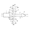
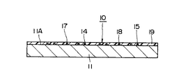
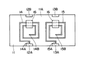
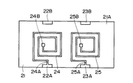
まず、図1ないし図9は第1の参考例によるチップ型コイル部品を示し、図において、10は信号線3,4の途中に接続されたチップ型コイル部品で、該チップ型コイル部品10は、後述の基板11、外部電極12A〜13B、スパイラルコイル14,15、絶縁膜16、引出し用配線17,18、保護膜19によって構成されている。
【0023】
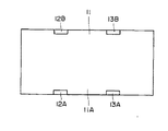
11はチップ型コイル部品10の外形をなす基板で、該基板11は、例えばアルミナ系セラミックス、ガラス等の低誘電率な絶縁材料によって形成され、略長方形の板状に形成されている。
【0024】
12A,13Aは長方形状をなす基板11の一側の長辺に2個設けられた外部電極、12B,13Bは同じく基板11の他側の長辺に2個設けられた他の外部電極をそれぞれ示し、該各外部電極12A〜13Bは基板11の端面(側面)から表面11Aに亘って形成されている。そして、外部電極12A,12Bにはスパイラルコイル14の両端側が接続され、外部電極13A,13Bにはスパイラルコイル15の両端側が接続されている。
【0025】
14,15は基板11の表面11Aに設けられたスパイラルコイルで、該各スパイラルコイル14,15は、微細加工技術としてスパッタリング、蒸着等によって形成された導電性金属材料による金属薄膜をフォトリソグラフィ等によって形成されたマスクを用いてエッチング処理を施すことによってアレイ状に形成されている。
【0026】
そして、スパイラルコイル14,15は、相互に同形、同大の形状をなし、外周側に位置する一端部14A,15Aから内周側に位置する他端部14B,15Bに向かって例えば略四角形の渦巻き形状をなしている。また、スパイラルコイル14,15は、その一端部14A,15Aが外部電極12A,13Aに接続され、その他端部14B,15Bが後述の引出し用配線17,18に接続されている。
【0027】
16,16はスパイラルコイル14,15を部分的に覆う絶縁膜で、該各絶縁膜16は、スパイラルコイル14,15の他端部14B,15Bと外部電極12B,13Bとの間に位置し、これらの間を横切るスパイラルコイル14,15を覆っている。そして、絶縁膜16は、ポリイミド等の低誘電率を有する絶縁性樹脂材料によって略四角形の薄膜状に形成され、その表面側に設けられる引出し用配線17,18とスパイラルコイル14,15との間を電気的に絶縁している。
【0028】
17,18はスパイラルコイル14,15の他端部14B,15Bと外部電極12B,13Bとの間に直線状に延伸して設けられた引出し用配線で、該引出し用配線17,18は、導電性金属材料による金属薄膜からなり、絶縁膜16の表面にスパイラルコイル14等と同様の微細加工を施すことによって形成されている。そして、引出し用配線17,18は、スパイラルコイル14,15の他端部14B,15Bと外部電極12B,13Bとの間を電気的に接続している。
【0029】
19はスパイラルコイル14,15、引出し用配線17,18等を覆って基板11の表面11A全面に形成された保護膜で、該保護膜19は、ポリイミド等の絶縁性樹脂材料によって薄膜状に形成されている。そして、保護膜19は、外部応力からスパイラルコイル14,15等を保護すると共に、スパイラルコイル14,15等の損傷を防ぎ、信頼性を向上させている。また、保護膜19の誘電率は低い値に設定され、各スパイラルコイル14,15内で発生する浮遊容量を抑制している。
【0030】
第1の参考例によるチップ型コイル部品10は上述の如き構成を有するもので、次にその製造方法について図4ないし図9を参照しつつ説明する。
【0031】
まず、図4に示すように基板11の外周側に外部電極12A〜13Bを設ける。次に、図5に示すように基板11の表面11Aには、スパッタリング、真空蒸着等によって導電性金属材料からなる金属薄膜Mを全面に亘って形成する。
【0032】
次に、金属薄膜Mの表面にフォトレジストを塗布すると共に、フォトリソグラフィを用いて外部電極12A〜13B、スパイラルコイル14,15と同形状のマスクを形成する。この状態で、エッチング処理を施すことによって、基板11の表面11Aには、図6に示すように2個のスパイラルコイル14,15を同一工法によって一緒に形成する。このとき、スパイラルコイル14,15の一端部14A,15Aは、外部電極12A,13Aに接続される。
【0033】
その後、図7に示すようにスパイラルコイル14,15の他端部14B,15Bと外部電極12B,13Bとの間には、絶縁性樹脂材料からなる絶縁膜16を形成する。このとき、絶縁膜16は、スパイラルコイル14,15の内周側から外周側に向かって帯状に延び、スパイラルコイル14,15を部分的に覆う。
【0034】
この状態で、再びスパッタリング等の微細加工を施すことによって、絶縁膜16の表面側には、図8に示すように引出し用配線17,18を形成する。このとき、引出し用配線17,18の両端は、スパイラルコイル14,15の他端部14B,15Bと外部電極12B,13Bとにそれぞれ接続される。
【0035】
最後に、図9に示すように基板11の表面11Aには、全面に亘ってスパイラルコイル14,15等を覆う保護膜19を形成する。
【0036】
かくして、第1の参考例によるチップ型コイル部品10は上述の製造方法によって形成されるものであり、図1に示すように高周波デバイス1,2間の信号線3,4に外部電極12A,13Aを接続すると共に、外部電極12B,13Bをアースに接続することによって高周波デバイス1,2間のインピーダンスマッチングをとることができる。
【0037】
然るに、第1の参考例では、2個のスパイラルコイル14,15を基板11の表面11A側に位置して同一平面上に設けたから、2個のスパイラルコイル14,15を基板11上に一緒に形成することができる。このため、製造工程の相違によって2個のスパイラルコイル14,15のインダクタンス値がばらつくことがなく、スパイラルコイル14,15のインダクタンス値を略等しい値に設定することができる。これにより、2本の信号線3,4を略等しい状態にマッチングさせることができるから、ノイズの混入を防ぎ、信号の伝送特性を向上させることができる。
【0038】
また、第1の参考例では、単一平面をなす基板11の表面11Aに2個のスパイラルコイル14,15を形成したから、例えば基板上に多数の層を積層してコイルを形成する積層型のコイル部品に比べて、厚さ方向に対するスパイラルコイル14,15のばらつきを少なくし、スパイラルコイル14,15のインダクタンス値を略等しい値に設定することができる。
【0039】
一方、従来技術のように2つのチップ型コイル部品を配置する場合には、各チップ型コイル部品毎に実装方向、実装位置にずれが生じることがあり、これによるインダクタンス値にばらつきが生じる傾向もあった。これに対し、第1の参考例では、単一のチップ型コイル部品10に2個のスパイラルコイル14,15を備える構成としたから、チップ型コイル部品10を取付けることによって2個のスパイラルコイル14,15を位置決めすることができ、実装方向、実装位置にずれによるインダクタンス値のばらつきをも防ぐことができる。
【0040】
また、2個のスパイラルコイル14,15を単一の基板11に形成したから、高周波デバイス1,2間に単一のチップ型コイル部品10を配置すればよく、従来技術のように2つのチップ型コイル部品を配置する場合に比べてチップ型コイル部品10による占有面積を小さくすることができる。このため、小形化が要求される携帯電話器等であっても容易に適用することができる。
【0041】
さらに、高周波デバイス1,2間に単一のチップ型コイル部品10を取付けるから、実装部品の点数を削減でき、製造コストを低減することができる。
【0042】
また、2個のスパイラルコイル14,15を同一工法によって一緒に形成したから、製造工程の相違によるスパイラルコイル14,15の形状の相違をなくすことができる。
【0043】
特に、第1の参考例では、スパイラルコイル14,15をスパッタリング、蒸着、フォトリソグラフィによる微細加工技術を用いて形成したから、スパイラルコイル14,15の膜厚をスパッタリング、蒸着によって略等しい値に設定できると共に、その平面形状(渦巻き形状)もフォトリソグラフィによって略等しい形状に設定できる。このため、スパイラルコイル14,15のインダクタンス値を略等しい値に設定することができる。
【0044】
次に、図10ないし図15は第2の参考例によるチップ型コイル部品を示し、第2の参考例の特徴は、基板の表面側には第1のスパイラルコイルを覆って絶縁膜を設け、該絶縁膜を挟んで絶縁膜の表面側には第1のスパイラルコイルと直列接続した第2のスパイラルコイルを設けたことにある。
【0045】
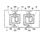
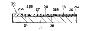
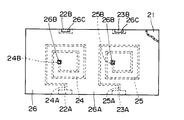
20は第2の参考例によるチップ型コイル部品で、該チップ型コイル部品20は、後述の基板21、外部電極22A〜23B、第1のスパイラルコイル24,25、絶縁膜26、第2のスパイラルコイル27,28、保護膜29等によって構成されている。
【0046】
21はチップ型コイル部品20の外形をなす基板で、該基板21は、第1の参考例と同様に低誘電率な絶縁材料によって形成され、略長方形の板状に形成されている。
【0047】
22A,23Aは基板21の一側の長辺に2個設けられた外部電極、22B,23Bは基板21の他側の長辺に2個設けられた他の外部電極をそれぞれ示し、外部電極22A,23Aには第1のスパイラルコイル24,25の一端部24A,25Aがそれぞれ接続され、外部電極22B,23Bには第2のスパイラルコイル27,28の他端部27B,28Bがそれぞれ接続されている。
【0048】
24,25は基板21の表面21Aに設けられた第1のスパイラルコイルで、該各スパイラルコイル24,25は、第1の参考例によるスパイラルコイル14,15と同様に微細加工技術を用いて一緒に形成されている。そして、スパイラルコイル24,25は、相互に同形、同大の形状をなし、外周側に位置する一端部24A,25Aから内周側に位置する他端部24B,25Bに向かって例えば略四角形の渦巻き形状をなしている。また、スパイラルコイル24,25は、その一端部24A,25Aが外部電極22A,23Aに接続され、その他端部24B,25Bが後述する第2のスパイラルコイル27,28に接続されている。
【0049】
26はスパイラルコイル24,25を覆って基板21の表面21A全面に設けられた絶縁膜で、該絶縁膜26は、低誘電率を有する絶縁性樹脂材料によって薄膜状に形成されている。また、絶縁膜26には、スパイラルコイル24,25の他端部24B,25Bに対応する位置に貫通孔26B,26Bが設けられると共に、外部電極22B,23Bと対応する位置に貫通孔26C,26Cが設けられている。
【0050】
27,28は基板21との間に絶縁膜26を挟み、絶縁膜26の表面26Aに設けられた第2のスパイラルコイルで、該スパイラルコイル27,28は、微細加工技術を用いて一緒に形成され、相互に同形、同大の形状をなしている。また、第2のスパイラルコイル27,28は、第1のスパイラルコイル24,25と同一の巻線方向をなし、内周側に位置する一端部27A,28Aから外周側に位置する他端部27B,28Bに向かって例えば略四角形の渦巻き形状となっている。さらに、第2のスパイラルコイル27,28は、第1のスパイラルコイル24,25に重ね合わせた位置に設けられている。
【0051】
また、スパイラルコイル27,28は、その一端部27A,28Aが貫通孔26Bを通じて第1のスパイラルコイル24,25の他端部24B,25Bに接続され、その他端部27B,28Bが貫通孔26Cを通じて外部電極22B,23Bに接続されている。これにより、第2のスパイラルコイル27,28は、第1のスパイラルコイル24,25に直列接続され、これらに発生する磁束を増加させ、インダクタンス値を増加させている。
【0052】
29は第2のスパイラルコイル27,28を覆って絶縁膜26の表面26A全面に形成された保護膜で、該保護膜29は、第1の参考例による保護膜19と同様にポリイミド等の絶縁性樹脂材料によって薄膜状に形成されている。
【0053】
第2の参考例によるチップ型コイル部品20は上述の如き構成を有するもので、次にその製造方法について図12ないし図15を参照しつつ説明する。
【0054】
まず、第1の参考例と同様に基板21の外周側に外部電極22A〜23Bを設ける。そして、図12に示すように基板21の表面21Aには、微細加工技術として第1の参考例に係る図5の場合と同様にスパッタリング、真空蒸着等によって金属薄膜(図示せず)を形成した後、該金属薄膜をフォトリソグラフィによって形成したマスクを用いてエッチング処理を施すことによって、第1のスパイラルコイル24,25を形成する。このとき、スパイラルコイル24,25の一端部24A,25Aは外部電極22A,23Aに接続する。
【0055】
次に、図13に示すように基板21にはスパイラルコイル24,25を覆って絶縁膜26を形成する。このとき、絶縁膜26には、スパイラルコイル24,25の他端部24B,25Bに対応した位置にそれぞれ貫通孔26Bを設けると共に、外部電極22B,23Bと対応した位置にそれぞれ貫通孔26Cを設ける。
【0056】
この状態で、図14に示すように絶縁膜26の表面26Aには、微細加工技術として第1の参考例に係る図5の場合と同様にスパッタリング、真空蒸着等によって金属薄膜(図示せず)を形成した後、該金属薄膜をフォトリソグラフィによって形成したマスクを用いてエッチング処理を施すことによって、第2のスパイラルコイル27,28を形成する。このとき、スパイラルコイル27,28は、その一端部27A,28Aが貫通孔26Bを通じて第1のスパイラルコイル24,25の他端部24B,25Bに接続し、その他端部27B,28Bが貫通孔26Cを通じて外部電極22B,23Bに接続する。
【0057】
最後に、絶縁膜26の表面26Aには、図15に示すようにその全面に亘って第2のスパイラルコイル27,28を覆う保護膜29を形成する。
【0058】
かくして、第2の参考例でも第1の参考例と同様の作用効果を得ることができる。しかし、第2の参考例では、基板21の表面21A側には絶縁膜26を挟んで第1のスパイラルコイル24,25と直列接続した第2のスパイラルコイル27,28を設けたから、第1のスパイラルコイル24,25と第2のスパイラルコイル27,28とによって発生する磁束を増加でき、これらによるインダクタンス値を増加させることができる。このため、第1のスパイラルコイル24,25ではインダクタンス値が不足する場合でも、第2のスパイラルコイル27,28を接続し、容易に必要なインダクタンス値を設定することができる。
【0059】
また、第1のスパイラルコイル24,25は微細加工技術を用いて一緒に形成すると共に、第2のスパイラルコイル27,28も微細加工技術を用いて一緒に形成する。このため、第1のスパイラルコイル24,25のインダクタンス値を略等しい値に設定できると共に、第2のスパイラルコイル27,28のインダクタンス値も略等しい値に設定することができる。このため、第1,第2のスパイラルコイル24,27による合成インダクタンス値と第1,第2のスパイラルコイル25,28による合成インダクタンス値とを略等しい値に設定できる。
【0060】
なお、第2の参考例では第1のスパイラルコイル24,25と第2のスパイラルコイル27,28とを2層重ね合わせる構成としたが、3層以上のスパイラルコイルを重ね合わせる構成としてもよい。
【0061】
次に、図16は第3の参考例によるチップ型コイル部品を示し、第3の参考例の特徴は、相互に隣合う2個のスパイラルコイルの巻線部分を非平行に配置する構成したことにある。
【0062】
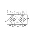
30は第3の参考例によるチップ型コイル部品で、該チップ型コイル部品30は、第1の参考例によるチップ型コイル部品10と同様に基板31に4個の外部電極32A〜33Bを設けた状態で、後述のスパイラルコイル34,35、絶縁膜36、引出し用配線37,38等を形成することによって構成されている。
【0063】
34,35は基板31の表面31Aに設けられたスパイラルコイルで、該各スパイラルコイル34,35は、第1の参考例によるスパイラルコイル14,15と同様に微細加工技術を用いて形成され、相互に同形、同大の形状をなすと共に、外周側に位置する一端部34A,35Aから内周側に位置する他端部34B,35Bに向かって例えば略四角形(菱形)の渦巻き形状をなしている。また、スパイラルコイル34,35の表面側には絶縁膜36を挟んで引出し用配線37,38が設けられている。そして、スパイラルコイル34,35は、その一端部34A,35Aが外部電極32A,33Aに接続され、その他端部34B,35Bが引出し用配線37,38を介して外部電極32B,33Bに接続されている。また、スパイラルコイル34,35等は絶縁性樹脂材料からなる保護膜(図示せず)によって覆われている。
【0064】
一方、四角形状をなすスパイラルコイル34,35は互いにその角部34D,35Dが接近した状態で配置されている。このため、スパイラルコイル34,35のうち最外周側に位置して相互に隣合う巻線部分34C,35Cは、互いに非平行な状態で配置され、角部34D,35Dを挟んでL字状に屈曲して互いに離れる方向に向けて延びている。これにより、巻線部分34C,35Cは、接近した状態で平行に延伸する部分がなく、相互間の距離が広がっている。
【0065】
かくして、第3の参考例でも第1の参考例と同様の作用効果を得ることができる。しかし、第3の参考例では、相互に隣合うスパイラルコイル34,35の巻線部分34C,35Cは、互いに接近して配置された角部34D,35Dを有し、該角部34D,35Dを挟んでL字状に屈曲して互いに離れる方向に向けて延びる構成としたから、相互の辺部分が平行に延伸した場合に比べて、スパイラルコイル34,35間の磁気結合、静電結合を抑制することができ、スパイラルコイル34,35間のクロストークを低減できる。また、スパイラルコイル34,35間の磁気結合等によるインダクタンス値のばらつきを低減できるから、スパイラルコイル34,35のインダクタンス値を略等しい値にすることができる。
【0066】
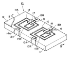
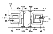
次に、図17および図18は実施の形態によるチップ型コイル部品を示し、本実施の形態の特徴は、基板には各スパイラルコイルに対応して2個の入出力電極と1個の接地電極とを設け、前記各スパイラルコイルは、その一端部を接続配線を用いて前記2個の入出力電極間に接続し、他端部を前記接地電極に接続する構成としたことにある。
【0067】
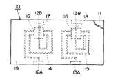
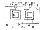
40は信号線3,4の途中に接続されたチップ型コイル部品で、該チップ型コイル部品40は、後述の基板41、入出力電極42A〜43B、接地電極44,45、接続配線46,47、スパイラルコイル48,49、絶縁膜50、引出し用配線51,52、保護膜(図示せず)等によって構成されている。
【0068】
41はチップ型コイル部品40の外形をなす基板で、該基板41は、第1の参考例と同様に低誘電率な絶縁材料によって形成され、略長方形の板状に形成されている。
【0069】
42A,42B,43A,43Bは2個のスパイラルコイル48,49に対応して、2個ずつ合計4個設けられた入出力電極で、該入出力電極42A,43Aは基板41の一側の長辺に2個配置され、他の入出力電極42B,43Bは基板41の他側の長辺に2個配置されている。また、入出力電極42A,42Bには接続配線46の両端側が接続され、入出力電極43A,43Bには接続配線47の両端側が接続されている。これら2本の接続配線46,47は、基板41を図17中の縦方向に横切って直線状に延びると共に、隣合う位置で互いに平行に配置されている。そして、入出力電極42A〜43Bは、信号線3,4に接続され、スパイラルコイル48,49に対して高周波デバイス1,2間の信号を入出力するものである。
【0070】
44,45は2個のスパイラルコイル48,49に対応して、1個ずつ合計2個設けられた接地電極で、該接地電極44,45は、基板41の短辺に1個ずつ配置されている。そして、接地電極44,45にはスパイラルコイル48,49の他端側が接続されると共に、実装基板(図示せず)を通じて接地されるものである。
【0071】
46,47は入出力電極42A,43Aと入出力電極42B,43Bとの間を接続する接続配線で、該接続配線46,47は、微細加工技術を用いることによってスパイラルコイル48,49と一緒に基板41の表面41Aに形成される。また、接続配線46,47は、基板41を横切って直線状に延びると共に、互いに平行に配置されている。
【0072】
48,49は基板41の表面41Aに設けられたスパイラルコイルで、該各スパイラルコイル48,49は、基板41のうち2本の接続配線46,47を挟んで図17中の横方向の両側位置にそれぞれ配置され、接続配線46,47と接地電極44,45との間にそれぞれ配置されている。また、スパイラルコイル48,49は、第1の参考例によるスパイラルコイル14,15と同様に微細加工技術を用いて形成され、相互に同形、同大の形状をなすと共に、外周側に位置する一端から内周側に位置する他端に向かって例えば略四角形の渦巻き形状をなしている。そして、スパイラルコイル48,49は、その一端部48A,49Aが接続配線46,47を用いて入出力電極42A,42Bと入出力電極43A,43Bとに接続され、その他端部48B,49Bが後述の引出し用配線51,52に接続されている。このとき、2個のスパイラルコイル48,49は、2本の接続配線46,47にそれぞれ接続された状態を含めて互いに対称な形状に形成されている。
【0073】
50,50はスパイラルコイル48,49を部分的に覆う絶縁膜で、該絶縁膜50は、絶縁性樹脂材料によって略四角形の薄膜状に形成されている。そして、絶縁膜50は、スパイラルコイル48,49の他端部48B,49Bと接地電極44,45との間に位置し、これらの間を横切るスパイラルコイル48,49を覆っている。
【0074】
51,52はスパイラルコイル48,49の他端部48B,49Bと接地電極44,45との間に直線状に延伸して設けられた引出し用配線で、該引出し用配線51,52は、導電性金属材料による金属薄膜からなり、絶縁膜50の表面にスパイラルコイル48,49と同様の微細加工を施すことによって形成されている。また、基板41の表面41Aには全面に亘って保護膜(図示せず)が設けられ、該保護膜によって引出し用配線51,52等は覆われている。
【0075】
かくして、本実施の形態でも第1の参考例と同様の作用効果を得ることができる。しかし、本実施の形態では、スパイラルコイル48,49の一端部48A,49Aを接続配線46,47を用いて入出力電極42A〜43Bに接続し、他端部48B,49Bを接地電極44,45に接続したから、信号線3,4に入出力電極42A〜43Bを接続し、接地電極44,45をアースに接続することによって、容易に高周波デバイス1,2間のマッチングをとることができる。
【0076】
また、入出力電極42A,43Aと入出力電極42B,43Bとは接続配線46,47によって接続する構成としたから、信号線3,4に入出力電極42A〜43Bを接続したときには、接続配線46,47を通じて高周波デバイス1,2間の信号を伝送することができる。このため、高周波デバイス1,2間を接続するワイヤボンディング等を別途設ける必要がなく、高周波デバイス1,2間に容易にチップ型コイル部品40を取付けることができる。
【0077】
なお、前記実施の形態では基板41に2個のスパイラルコイル48,49を設けた場合を例に挙げて説明したが、本発明はこれに限らず、基板の表面に3個以上のスパイラルコイルを形成する構成としてもよい。また、前記実施の形態のチップ型コイル部品は、第1の参考例と同様の製造方法を用いて形成してもよい。
【0078】
また、前記実施の形態では、2個のスパイラルコイル48,49に対応して2つの絶縁膜50を設けるものとしたが、第2の参考例と同様に単一の絶縁膜を用いる構成としてもよい。この場合、第2の参考例と同様に、基板の表面側には第1のスパイラルコイルを覆って絶縁膜を設け、該絶縁膜を挟んで絶縁膜の表面側には第1のスパイラルコイルと直列接続した第2のスパイラルコイルを設ける構成としてもよく、第2の参考例と同様の製造方法を用いて形成してもよい。さらに、第3の参考例と同様に、相互に隣合う2個のスパイラルコイルの巻線部分を非平行に配置する構成としてもよい。
【0079】
【発明の効果】
以上詳述した如く、請求項1の発明によれば、スパイラルコイルを基板の表面側に位置して同一平面上に複数個設けたから、製造工程の相違によるスパイラルコイルのインダクタンス値のばらつきを抑制することができ、基板上に設けた複数個のスパイラルコイルのインダクタンス値を略等しい値に設定することができる。このため、例えばチップ型コイル部品をインピーダンスマッチング用としてバランス方式の2本の信号線に接続するときには、2本の信号線で略等しい状態にマッチングさせることができ、ノイズの混入を防ぎ、信号の伝送特性を向上させることができる。
【0080】
また、単一のチップ型コイル部品に複数個のスパイラルコイルを備える構成としたから、チップ型コイル部品を取付けることによって複数個のスパイラルコイルを位置決めすることができ、実装方向、実装位置にずれによるインダクタンス値のばらつきをも防ぐことができる。
【0081】
さらに、複数個のスパイラルコイルを単一の基板に形成したから、高周波デバイス間に単一のチップ型コイル部品を配置することによって複数の信号線のマッチングをとることができる。このため、従来技術のように別々のチップ型コイル部品を複数個配置する場合に比べてチップ型コイル部品による占有面積を小さくすることができ、小形化が要求される携帯電話器等であっても容易に適用することができる。また、高周波デバイス間に単一のチップ型コイル部品を取付けるから、実装部品の点数を削減でき、製造コストを低減することができる。
【0082】
また、基板には両端側に入出力端子が接続された複数本の接続配線を設けると共に、複数個のスパイラルコイルは、その一端側を互いに異なる接続配線に接続し、他端側を互いに異なる接地端子に接続する構成とした。このため、例えばチップ型コイル部品をインピーダンスマッチング用として高周波デバイス間の信号線に接続するときでも、信号線の途中に入出力端子をそれぞれ接続し、接地端子をアースに接続することによって容易にインピーダンスマッチングをとることができる。また、接続配線を通じて信号を伝送することができるから、信号伝送用のワイヤボンディング等を別途設ける必要がなく、生産性を向上させ、製造コストを低減することができる。
【0083】
請求項2の発明によれば、複数個のスパイラルコイルは同一工法によって一緒に形成する構成としたから、製造工法、製造条件によるインダクタンス値のばらつきを防ぎ、これら複数個のスパイラルコイルのインダクタンス値を略等しい値に設定することができる。
【0084】
請求項3の発明によれば、複数個のスパイラルコイルのうち相互に隣合う2個のスパイラルコイルの巻線部分は、互いに接近して配置された角部を有し、該角部を挟んでL字状に屈曲して互いに離れる方向に向けて延びる構成としたから、隣合う2個のスパイラルコイル間での磁気結合、静電結合を抑制でき、これらのスパイラルコイル間のクロストークを低減できると共に、磁気結合等に伴うインダクタンスのばらつきを低減できる。
【0085】
請求項4の発明によれば、基板の表面側には複数個のスパイラルコイルを覆って絶縁膜を設け、該絶縁膜を挟んで該絶縁膜の表面側には前記各スパイラルコイルと直列接続した他のスパイラルコイルを設けたから、各スパイラルコイル等によって発生する磁束を増加させ、これらのインダクタンス値を増加させることができる。
【0086】
請求項5の発明によれば、複数個のスパイラルコイルは、スパッタリングまたは蒸着によって金属薄膜を形成し、フォトリソグラフィを用いて該金属薄膜の平面形状を成形することによって一緒に形成した。これにより、スパッタリングまたは蒸着によって複数個のスパイラルコイルの膜厚を略等しい値に設定でき、フォトリソグラフィによって複数個のスパイラルコイルの平面形状を略等しい形状に設定できる。このため、複数個のスパイラルコイルのインダクタンス値を略等しい値に設定することができる。
【0087】
請求項6の発明によれば、基板には、バランス方式により互いに逆位相の信号を伝送するために当該基板を横切って直線状に延びると共に互いに平行に配置された2本の接続配線と、互いに異なる接続配線に接続された2個のスパイラルコイルとを設けた。このため、請求項6の発明でも、請求項1の発明と同様の効果を得ることができる。
【0088】
また、請求項7の発明のように、2個のスパイラルコイルは、2本の接続配線にそれぞれ接続された状態を含めて互いに対称な形状に形成してもよい。
【図面の簡単な説明】
【図1】 第1の参考例によるチップ型コイル部品を高周波デバイスに接続した状態を示す電気回路図である。
【図2】 第1の参考例によるチップ型コイル部品を示す斜視図である。
【図3】 チップ型コイル部品を図2中の矢示III−III方向からみた断面図である。
【図4】 基板に外部電極を取付けた状態を示す平面図である。
【図5】 基板に金属薄膜を形成した状態を示す平面図である。
【図6】 基板にスパイラルコイルを形成した状態を示す平面図である。
【図7】 基板にスパイラルコイルの一部を覆って絶縁膜を形成した状態を示す平面図である。
【図8】 絶縁膜を挟んで基板に引出し用配線を形成した状態を示す平面図である。
【図9】 スパイラルコイル等を覆って基板に保護膜を形成した状態を示す平面図である。
【図10】 第2の参考例によるチップ型コイル部品を絶縁膜の位置で分解した状態で示す分解斜視図である。
【図11】 チップ型コイル部品を図3と同様の位置からみた断面図である。
【図12】 基板に第1のスパイラルコイルを形成した状態を示す平面図である。
【図13】 基板全面に第1のスパイラルコイルを覆って絶縁膜を形成した状態を示す平面図である。
【図14】 絶縁膜の表面に第2のスパイラルコイルを形成した状態を示す平面図である。
【図15】 第2のスパイラルコイル等を覆って基板に保護膜を形成した状態を示す平面図である。
【図16】 第3の参考例によるチップ型コイル部品を保護膜を省いた状態で示す平面図である。
【図17】 本発明の実施の形態によるチップ型コイル部品を保護膜を省いた状態で示す平面図である。
【図18】 実施の形態によるチップ型コイル部品を高周波デバイスに接続した状態を示す電気回路図である。
【図19】 従来技術によるチップ型コイル部品を高周波デバイスに接続した状態を示す電気回路図である。
【符号の説明】
10,20,30,40 チップ型コイル部品
11,21,31,41 基板
14,15,34,35,48,49 スパイラルコイル
24,25 第1のスパイラルコイル
26 絶縁膜
27,28 第2のスパイラルコイル(他のスパイラルコイル)
42A,42B,43A,43B 入出力電極(入出力端子)
44,45 接地電極(接地端子)
46,47 接続配線[0001]
BACKGROUND OF THE INVENTION
The present invention relates to a chip-type coil component in which a spiral coil is formed on a substrate, and more particularly to a chip-type coil component suitable for use in impedance matching between high-frequency devices such as mobile phones.
[0002]
[Prior art]
In general, a chip-type coil component is known in which a spiral coil is provided on a substrate. Further, in recent years, in a high-frequency device that processes high-frequency signals, two high-
[0003]
In the prior art, single chip-
[0004]
[Problems to be solved by the invention]
However, when two chip-
[0005]
Further, since the single chip-
[0006]
Furthermore, since it is necessary to provide two chip-
[0007]
The present invention has been made in view of the above-described problems, and an object of the present invention is to provide a chip-type coil component that can reduce variation in inductance value, reduce an occupied area, and reduce manufacturing costs. It is in.
[0008]
[Means for Solving the Problems]
In order to solve the above-mentioned problem, the invention of claim 1 is a chip-type coil component comprising a substrate and a spiral coil provided on the surface side of the substrate.The substrate includes a plurality of connection wirings extending linearly across the substrate and arranged in parallel to each other, input / output terminals respectively connected to both ends of each connection wiring, and a plurality of grounding wires And grounding terminals,The spiral coil is,Provide a plurality on the same plane located on the surface side of the substrateThe plurality of spiral coils are configured such that one end side thereof is connected to the different connection wirings and the other end side thereof is connected to the different ground terminals.It is characterized by that.
[0009]
With this configuration, a plurality of spiral coils can be formed together on the same plane on the substrate surface side. For this reason, the variation in the inductance value of the spiral coil due to the difference in the manufacturing process can be suppressed, and the inductance values of the plurality of spiral coils provided on the substrate can be set to substantially equal values.
[0010]
In addition, since a connection line extending linearly across the substrate is provided and a spiral coil is connected to the connection line, for example, even when connecting a chip-type coil component to a signal line between high-frequency devices for impedance matching The input / output terminals can be connected in the middle of the signal lines, and signals can be transmitted through the connection wiring provided between the two input / output terminals.
[0011]
The invention of
[0012]
As a result, multiple on the board by the same construction methodPiecesThese spiral coils can be formed togetherPiecesThe inductance value of the spiral coil can be set to a substantially equal value.
[0013]
In the invention of
[0014]
This makes 2 adjacentPiecesMagnetic coupling and electrostatic coupling between the spiral coils can be suppressed, crosstalk between these spiral coils can be reduced, and variation in inductance caused by magnetic coupling or the like can be reduced.
[0015]
According to a fourth aspect of the present invention, there is provided the plurality of substrates on the surface side of the substrate.PiecesAn insulating film is provided so as to cover the spiral coil, and another spiral coil connected in series with each spiral coil is provided on the surface side of the insulating film with the insulating film interposed therebetween.The other end of each spiral coil is connected to each ground terminal via the other spiral coil.That is.
[0016]
As a result, each spiral coil can be connected to another spiral coil in series to increase the inductance value.
[0017]
The invention of claim 5 includes a plurality ofPiecesSpiral coil,SputteringOrVapor depositionTo form a metal thin film,PhotolithographyTogether by shaping the planar shape of the metal thin film usingIt is in forming.
[0018]
This allows multiplePiecesThe thickness of the spiral coil can be set to a substantially equal value by sputtering and vapor deposition, and the planar shape can be set to a substantially equal shape by photolithography. For this reason, multiplePiecesThe inductance value of the spiral coil can be set to a substantially equal value.
[0019]
The invention of claim 6A board, two connection wires provided on the board for transmitting signals in opposite phases in a balanced manner, extending linearly across the board and arranged parallel to each other, and provided on the board; Input / output terminals respectively connected to both ends of each connection wiring, two ground terminals provided on the substrate for grounding, and 2 provided on the same plane on the surface side of the substrate Each of the two spiral coils is disposed on both sides of the two connection wires, and one end side thereof is connected to the different connection wires, and the other end side is connected to each other. It is configured to connect to different ground terminals.
[0020]
The invention of
[0021]
DETAILED DESCRIPTION OF THE INVENTION
In the following, as a chip-type coil component according to the present invention, 2PiecesA case where the spiral coil is provided will be described as an example, and will be described in detail with reference to the accompanying drawings. In addition,Each reference example shown below andIn the embodiment, the same components as those in the prior art are denoted by the same reference numerals, and the description thereof is omitted.
[0022]
First, FIG. 1 to FIG.Reference exampleIn the figure,
[0023]
Reference numeral 11 denotes a substrate that forms the outer shape of the chip-
[0024]
12A and 13A are two external electrodes provided on one long side of the
[0025]
[0026]
The spiral coils 14 and 15 have the same shape and the same size as each other. For example, the spiral coils 14 and 15 have a substantially rectangular shape from the one
[0027]
16 and 16 are insulating films that partially cover the spiral coils 14 and 15, each insulating
[0028]
[0029]
[0030]
First reference exampleThe chip-
[0031]
First, as shown in FIG. 4,
[0032]
Next, a photoresist is applied to the surface of the metal thin film M, and a mask having the same shape as the
[0033]
Thereafter, as shown in FIG. 7, an insulating
[0034]
In this state, by performing fine processing such as sputtering again, lead
[0035]
Finally, as shown in FIG. 9, a
[0036]
Thus,First reference exampleThe chip-
[0037]
However,First reference exampleThen, 2PiecesSince the spiral coils 14 and 15 are located on the surface 11A side of the substrate 11 and provided on the same plane, 2PiecesThe spiral coils 14 and 15 can be formed on the substrate 11 together. For this reason, 2PiecesThe inductance values of the spiral coils 14 and 15 do not vary, and the inductance values of the spiral coils 14 and 15 can be set to substantially equal values. As a result, 2BookThus, the
[0038]
Also,First reference exampleThen, 2 on the surface 11A of the substrate 11 forming a single plane.PiecesSince the spiral coils 14 and 15 are formed, the variation of the spiral coils 14 and 15 in the thickness direction is reduced compared to, for example, a laminated coil component in which a number of layers are laminated on a substrate to form a coil. The inductance values of the spiral coils 14 and 15 can be set to substantially equal values.
[0039]
On the other hand, when two chip-type coil components are arranged as in the prior art, the mounting direction and the mounting position may be different for each chip-type coil component, and the inductance value tends to vary. there were. In contrast,First reference exampleThen, a single chip-
[0040]
2PiecesSince the spiral coils 14 and 15 are formed on the single substrate 11, the single chip-
[0041]
Furthermore, since the single chip-
[0042]
2PiecesSince the spiral coils 14 and 15 are formed together by the same method, the difference in the shape of the spiral coils 14 and 15 due to the difference in the manufacturing process can be eliminated.
[0043]
In particular,First reference exampleThen, since the spiral coils 14 and 15 are formed by using a fine processing technique by sputtering, vapor deposition, and photolithography, the film thickness of the spiral coils 14 and 15 can be set to a substantially equal value by sputtering and vapor deposition, and the planar shape ( The spiral shape can also be set to a substantially equal shape by photolithography. For this reason, the inductance values of the spiral coils 14 and 15 can be set to substantially equal values.
[0044]
Next, FIG. 10 to FIG.Reference exampleShows chip type coil parts bySecond reference exampleIs characterized in that an insulating film is provided on the surface side of the substrate so as to cover the first spiral coil, and the second spiral coil connected in series with the first spiral coil on the surface side of the insulating film across the insulating film It is in having established.
[0045]
20Second reference exampleThe chip-
[0046]
21 is a substrate forming the outer shape of the chip-
[0047]
[0048]
[0049]
An insulating
[0050]
[0051]
The spiral coils 27 and 28 have one
[0052]
A
[0053]
Second reference exampleThe chip-
[0054]
First, firstReference exampleSimilarly, external electrodes 22 </ b> A to 23 </ b> B are provided on the outer peripheral side of the
[0055]
Next, as shown in FIG. 13, an insulating
[0056]
In this state, as shown in FIG. 14, the
[0057]
Finally, a
[0058]
Thus,Second reference exampleBut firstReference exampleThe same effect can be obtained. But,Second reference exampleThen, since the second spiral coils 27 and 28 connected in series with the first spiral coils 24 and 25 are provided on the
[0059]
In addition, the first spiral coils 24 and 25 are formed together using a fine processing technique, and the second spiral coils 27 and 28 are also formed together using a fine processing technique. For this reason, the inductance values of the first spiral coils 24 and 25 can be set to substantially equal values, and the inductance values of the second spiral coils 27 and 28 can also be set to substantially equal values. Therefore, the combined inductance value by the first and second spiral coils 24 and 27 and the combined inductance value by the first and second spiral coils 25 and 28 can be set to substantially equal values.
[0060]
The secondReference exampleThen, the first spiral coils 24 and 25 and the second spiral coils 27 and 28 are stacked in two layers, but three or more layers of spiral coils may be stacked.
[0061]
Next, FIG. 16 shows the thirdReference exampleShows chip type coil parts byThird reference exampleThe features of 2 are adjacent to each otherPiecesThis is because the winding portions of the spiral coil are arranged non-parallel.
[0062]
30 isThird reference exampleThe chip-
[0063]
[0064]
On the other hand, the spiral coils 34 and 35 having a quadrangular shape are arranged with their
[0065]
Thus,Third reference exampleBut firstReference exampleThe same effect can be obtained. But,Third reference exampleThen, the winding
[0066]
Next, FIG. 17 and FIG.Is realThe chip-type coil component according to the embodiment is shown. The feature of the present embodiment is that the substrate is provided with two input / output electrodes and one ground electrode corresponding to each spiral coil, The one end is connected between the two input / output electrodes using a connection wiring, and the other end is connected to the ground electrode.
[0067]
[0068]
Reference numeral 41 denotes a substrate that forms the outer shape of the chip-type coil component 40.Reference exampleSimilarly, it is made of an insulating material having a low dielectric constant, and is formed in a substantially rectangular plate shape.
[0069]
42A, 42B, 43A, 43B is 2PiecesA total of four input / output electrodes are provided corresponding to the spiral coils 48 and 49, and two of the input /
[0070]
44 and 45 are 2PiecesA total of two ground electrodes corresponding to the spiral coils 48 and 49 are provided, and the
[0071]
[0072]
48 and 49 are spiral coils provided on the
[0073]
[0074]
[0075]
Thus, even in this embodiment, the firstReference exampleThe same effect can be obtained. However, in the present embodiment, one
[0076]
Further, since the input /
[0077]
BeforeRealIn the form of the baseBoard 41 to 2PiecesSpiral carpLe 4Although the case where 8, 49 is provided has been described as an example, the present invention is not limited to this, and three or more spiral coils may be formed on the surface of the substrate.The chip-type coil component of the above embodiment may be formed using the same manufacturing method as in the first reference example.
[0078]
Also beforeRealIn the embodiment, 2PiecesSpiral carpLe 4Two insulations corresponding to 8,
[0079]
【The invention's effect】
As described above in detail, according to the first aspect of the present invention, since the plurality of spiral coils are provided on the same plane and located on the surface side of the substrate, variations in the inductance value of the spiral coil due to differences in manufacturing processes are suppressed. Multiple provided on the substratePiecesThe inductance value of the spiral coil can be set to a substantially equal value. For this reason, for example, when a chip-type coil component is connected to two balanced signal lines for impedance matching, the two signal lines can be matched in substantially the same state, preventing noise from being mixed, Transmission characteristics can be improved.
[0080]
In addition, a single chip-type coil component has multiplePiecesBecause it has a configuration with a spiral coil, multiple chip-type coil components can be attachedPiecesThe spiral coil can be positioned, and variation in inductance value due to deviation in mounting direction and mounting position can also be prevented.
[0081]
More than onePiecesSince the spiral coil is formed on a single substrate, a plurality of signal lines can be matched by arranging a single chip-type coil component between high-frequency devices. For this reason, it is possible to reduce the area occupied by the chip-type coil component as compared with the case where a plurality of separate chip-type coil components are arranged as in the prior art, and it is a mobile phone or the like that is required to be downsized. Can also be applied easily. In addition, since a single chip-type coil component is attached between the high-frequency devices, the number of mounted components can be reduced, and the manufacturing cost can be reduced.
[0082]
In addition, the substrate is provided with a plurality of connection wires having input / output terminals connected to both ends, and the plurality of spiral coils are connected to different connection wires at one end and different grounds at the other end. It was set as the structure connected to a terminal. For this reason, for example, even when a chip-type coil component is connected to a signal line between high-frequency devices for impedance matching, the impedance can be easily obtained by connecting the input / output terminals in the middle of the signal line and connecting the ground terminal to the ground. Matching can be taken. Further, since the signal can be transmitted through the connection wiring, it is not necessary to separately provide a signal bonding wire bonding or the like, thereby improving the productivity and reducing the manufacturing cost.
[0083]
According to the invention of
[0084]
According to the invention of
[0085]
According to the invention of
[0086]
According to the invention of claim 5, a plurality ofPiecesSpiral coil,SputteringOrVapor depositionTo form a metal thin film,PhotolithographyTogether by shaping the planar shape of the metal thin film usingFormed. This, SputteringOrMultiple by vapor depositionPiecesThe thickness of the spiral coil can be set to approximately the same value.PiecesThe planar shape of the spiral coil can be set to a substantially equal shape. For this reason, multiplePiecesThe inductance value of the spiral coil can be set to a substantially equal value.
[0087]
According to invention of
[0088]
In addition, as in the seventh aspect of the invention, the two spiral coils may be formed symmetrically with respect to each other including the state of being connected to the two connection wires.
[Brief description of the drawings]
FIG. 1 FirstReference exampleIt is an electric circuit diagram which shows the state which connected the chip-type coil component by to a high frequency device.
FIG. 2 FirstReference exampleIt is a perspective view which shows the chip type coil components by.
3 is a cross-sectional view of the chip-type coil component as seen from the direction of arrows III-III in FIG. 2. FIG.
FIG. 4 is a plan view showing a state in which external electrodes are attached to a substrate.
FIG. 5 is a plan view showing a state in which a metal thin film is formed on a substrate.
FIG. 6 is a plan view showing a state in which a spiral coil is formed on a substrate.
FIG. 7 is a plan view showing a state in which an insulating film is formed on the substrate so as to cover a part of the spiral coil.
FIG. 8 is a plan view showing a state in which lead-out wiring is formed on a substrate with an insulating film interposed therebetween.
FIG. 9 is a plan view showing a state in which a protective film is formed on a substrate so as to cover a spiral coil and the like.
FIG. 10 shows the secondReference exampleIt is a disassembled perspective view shown in the state which decomposed | disassembled the chip-type coil component by 4 in the position of the insulating film.
11 is a cross-sectional view of the chip-type coil component as seen from the same position as in FIG. 3. FIG.
FIG. 12 is a plan view showing a state in which a first spiral coil is formed on a substrate.
FIG. 13 is a plan view showing a state in which an insulating film is formed on the entire surface of the substrate so as to cover the first spiral coil.
FIG. 14 is a plan view showing a state in which a second spiral coil is formed on the surface of the insulating film.
FIG. 15 is a plan view showing a state in which a protective film is formed on a substrate so as to cover a second spiral coil and the like.
FIG. 16 shows the thirdReference exampleIt is a top view which shows the chip type coil components by which the protective film was omitted.
FIG. 17The present inventionIt is a top view which shows the chip-type coil component by embodiment of this invention in the state which excluded the protective film.
FIG. 18FruitIt is an electric circuit diagram which shows the state which connected the chip-type coil component by embodiment to the high frequency device.
FIG. 19 is an electric circuit diagram showing a state in which a chip-type coil component according to the prior art is connected to a high-frequency device.
[Explanation of symbols]
10, 20, 30, 40 Chip type coil parts
11, 21, 31, 41 Substrate
14, 15, 34, 35, 48, 49 Spiral coil
24, 25 First spiral coil
26 Insulating film
27, 28 Second spiral coil (other spiral coil)
42A, 42B, 43A, 43B Input / output electrodes (input / output terminals)
44, 45 Ground electrode (ground terminal)
46, 47 Connection wiring
Claims (7)
前記基板には、当該基板を横切って直線状に延びると共に互いに平行に配置された複数本の接続配線と、該各接続配線の両端側にそれぞれ接続された入出力端子と、接地するための複数個の接地端子とを設け、
前記スパイラルコイルは、前記基板の表面側に位置して同一平面上に複数個設け、
該複数個のスパイラルコイルは、その一端側を互いに異なる前記接続配線に接続し、他端側を互いに異なる前記接地端子に接続する構成としたことを特徴とするチップ型コイル部品。In a chip-type coil component comprising a substrate and a spiral coil provided on the surface side of the substrate ,
The substrate includes a plurality of connection wirings extending linearly across the substrate and arranged in parallel to each other, input / output terminals respectively connected to both ends of each connection wiring, and a plurality of grounding wires And grounding terminals,
The spiral coils, a plurality provided on the same plane located on the surface side of the substrate,
The plurality of spiral coils have a configuration in which one end side is connected to the different connection wirings and the other end side is connected to the different ground terminals .
前記2個のスパイラルコイルは、前記2本の接続配線を挟んだ両側位置にそれぞれ配置され、その一端側を互いに異なる前記接続配線に接続し、他端側を互いに異なる前記接地端子に接続する構成としたチップ型コイル部品。 A substrate, two connection wirings provided on the substrate for transmitting signals in opposite phases in a balanced manner, extending linearly across the substrate and arranged in parallel with each other, and provided on the substrate; Input / output terminals respectively connected to both ends of each connection wiring, two ground terminals provided on the substrate for grounding, and 2 provided on the same plane located on the surface side of the substrate With a spiral coil,
The two spiral coils are respectively arranged on both sides of the two connection wires, and one end side thereof is connected to the different connection wires and the other end side is connected to the different ground terminals. and the chip-type coil component.
Priority Applications (1)
| Application Number | Priority Date | Filing Date | Title |
|---|---|---|---|
| JP2000296558A JP4626041B2 (en) | 2000-09-28 | 2000-09-28 | Chip coil components |
Applications Claiming Priority (1)
| Application Number | Priority Date | Filing Date | Title |
|---|---|---|---|
| JP2000296558A JP4626041B2 (en) | 2000-09-28 | 2000-09-28 | Chip coil components |
Publications (3)
| Publication Number | Publication Date |
|---|---|
| JP2002110422A JP2002110422A (en) | 2002-04-12 |
| JP2002110422A5 JP2002110422A5 (en) | 2007-09-27 |
| JP4626041B2 true JP4626041B2 (en) | 2011-02-02 |
Family
ID=18778817
Family Applications (1)
| Application Number | Title | Priority Date | Filing Date |
|---|---|---|---|
| JP2000296558A Expired - Lifetime JP4626041B2 (en) | 2000-09-28 | 2000-09-28 | Chip coil components |
Country Status (1)
| Country | Link |
|---|---|
| JP (1) | JP4626041B2 (en) |
Families Citing this family (7)
| Publication number | Priority date | Publication date | Assignee | Title |
|---|---|---|---|---|
| JP5083360B2 (en) * | 2010-04-02 | 2012-11-28 | セイコーエプソン株式会社 | Electronic substrate, semiconductor device and electronic equipment |
| KR101848721B1 (en) * | 2014-04-08 | 2018-04-13 | 가부시키가이샤 무라타 세이사쿠쇼 | High frequency module |
| JP2017168472A (en) * | 2016-03-14 | 2017-09-21 | 株式会社村田製作所 | Multilayer board |
| CN118151470A (en) | 2019-06-04 | 2024-06-07 | Lg伊诺特有限公司 | Camera module and camera device including the same |
| KR102863114B1 (en) * | 2019-06-12 | 2025-09-24 | 엘지이노텍 주식회사 | Camera module and Camera Apparatus including the same |
| CN218297031U (en) * | 2020-03-12 | 2023-01-13 | 雅马哈株式会社 | Displacement sensor and musical performance operating device |
| JP7235169B2 (en) * | 2020-05-22 | 2023-03-08 | 株式会社村田製作所 | Inductor mounting structure |
Family Cites Families (5)
| Publication number | Priority date | Publication date | Assignee | Title |
|---|---|---|---|---|
| JPH0787330B2 (en) * | 1985-06-20 | 1995-09-20 | 松下電器産業株式会社 | Balun coil |
| JPH07135116A (en) * | 1993-11-11 | 1995-05-23 | Matsushita Electric Ind Co Ltd | Composite part and manufacturing method thereof |
| JPH0817656A (en) * | 1994-06-29 | 1996-01-19 | T I F:Kk | Magnetic shielding method and magnetic shielding film forming method of semiconductor device |
| JPH0917679A (en) * | 1995-06-29 | 1997-01-17 | Mitsubishi Heavy Ind Ltd | Manufacture of laminated coil |
| JP3351738B2 (en) * | 1998-05-01 | 2002-12-03 | 太陽誘電株式会社 | Multilayer inductor and manufacturing method thereof |
-
2000
- 2000-09-28 JP JP2000296558A patent/JP4626041B2/en not_active Expired - Lifetime
Also Published As
| Publication number | Publication date |
|---|---|
| JP2002110422A (en) | 2002-04-12 |
Similar Documents
| Publication | Publication Date | Title |
|---|---|---|
| JP4500840B2 (en) | Multilayer balun and hybrid integrated circuit module and multilayer substrate | |
| CN111355495B (en) | High frequency module | |
| US6919777B2 (en) | Surface acoustic wave filter device | |
| CN1691220B (en) | coil parts | |
| US7579923B2 (en) | Laminated balun transformer | |
| JPWO2006134916A1 (en) | Multilayer filter | |
| JP4291164B2 (en) | Surface acoustic wave device | |
| US7439842B2 (en) | Laminated balun transformer | |
| US7236064B2 (en) | Laminated balun transformer | |
| CN107305807A (en) | Electronic unit | |
| JP2019050460A (en) | Laminate type electronic component | |
| JP2018207045A (en) | Electronic components | |
| JP4626041B2 (en) | Chip coil components | |
| CN111756350B (en) | Composite electronic components and electronic circuits | |
| JPH0738368A (en) | 180× phase shifter | |
| JP2010040882A (en) | Electronic component | |
| CN114334351A (en) | Coil component | |
| JP2003087074A (en) | Multilayer filter | |
| US20060022766A1 (en) | High frequency circuit module having non-reciprocal circuit element | |
| CN114334352A (en) | Coil component | |
| JP2018170315A (en) | Coil parts | |
| US12519449B2 (en) | Multilayer electronic component | |
| JP4085364B2 (en) | Non-reciprocal circuit element | |
| JPH1051257A (en) | LC low pass filter | |
| JP4130442B2 (en) | Front-end module for mobile communication equipment |
Legal Events
| Date | Code | Title | Description |
|---|---|---|---|
| A621 | Written request for application examination |
Free format text: JAPANESE INTERMEDIATE CODE: A621 Effective date: 20070719 |
|
| A521 | Request for written amendment filed |
Free format text: JAPANESE INTERMEDIATE CODE: A523 Effective date: 20070810 |
|
| A977 | Report on retrieval |
Free format text: JAPANESE INTERMEDIATE CODE: A971007 Effective date: 20091225 |
|
| A131 | Notification of reasons for refusal |
Free format text: JAPANESE INTERMEDIATE CODE: A131 Effective date: 20100112 |
|
| A521 | Request for written amendment filed |
Free format text: JAPANESE INTERMEDIATE CODE: A523 Effective date: 20100310 |
|
| TRDD | Decision of grant or rejection written | ||
| A01 | Written decision to grant a patent or to grant a registration (utility model) |
Free format text: JAPANESE INTERMEDIATE CODE: A01 Effective date: 20101012 |
|
| A01 | Written decision to grant a patent or to grant a registration (utility model) |
Free format text: JAPANESE INTERMEDIATE CODE: A01 |
|
| A61 | First payment of annual fees (during grant procedure) |
Free format text: JAPANESE INTERMEDIATE CODE: A61 Effective date: 20101025 |
|
| FPAY | Renewal fee payment (event date is renewal date of database) |
Free format text: PAYMENT UNTIL: 20131119 Year of fee payment: 3 |
|
| R150 | Certificate of patent or registration of utility model |
Ref document number: 4626041 Country of ref document: JP Free format text: JAPANESE INTERMEDIATE CODE: R150 Free format text: JAPANESE INTERMEDIATE CODE: R150 |