JP4703061B2 - Thin film circuit board manufacturing method and via forming board forming method - Google Patents
Thin film circuit board manufacturing method and via forming board forming method Download PDFInfo
- Publication number
- JP4703061B2 JP4703061B2 JP2001262359A JP2001262359A JP4703061B2 JP 4703061 B2 JP4703061 B2 JP 4703061B2 JP 2001262359 A JP2001262359 A JP 2001262359A JP 2001262359 A JP2001262359 A JP 2001262359A JP 4703061 B2 JP4703061 B2 JP 4703061B2
- Authority
- JP
- Japan
- Prior art keywords
- forming
- substrate
- hole
- main surface
- thin film
- Prior art date
- Legal status (The legal status is an assumption and is not a legal conclusion. Google has not performed a legal analysis and makes no representation as to the accuracy of the status listed.)
- Expired - Fee Related
Links
Images


Classifications
-
- H—ELECTRICITY
- H01—ELECTRIC ELEMENTS
- H01L—SEMICONDUCTOR DEVICES NOT COVERED BY CLASS H10
- H01L23/00—Details of semiconductor or other solid state devices
- H01L23/48—Arrangements for conducting electric current to or from the solid state body in operation, e.g. leads, terminal arrangements ; Selection of materials therefor
- H01L23/488—Arrangements for conducting electric current to or from the solid state body in operation, e.g. leads, terminal arrangements ; Selection of materials therefor consisting of soldered or bonded constructions
- H01L23/498—Leads, i.e. metallisations or lead-frames on insulating substrates, e.g. chip carriers
- H01L23/49827—Via connections through the substrates, e.g. pins going through the substrate, coaxial cables
-
- H—ELECTRICITY
- H01—ELECTRIC ELEMENTS
- H01L—SEMICONDUCTOR DEVICES NOT COVERED BY CLASS H10
- H01L21/00—Processes or apparatus adapted for the manufacture or treatment of semiconductor or solid state devices or of parts thereof
- H01L21/02—Manufacture or treatment of semiconductor devices or of parts thereof
- H01L21/04—Manufacture or treatment of semiconductor devices or of parts thereof the devices having at least one potential-jump barrier or surface barrier, e.g. PN junction, depletion layer or carrier concentration layer
- H01L21/48—Manufacture or treatment of parts, e.g. containers, prior to assembly of the devices, using processes not provided for in a single one of the subgroups H01L21/06 - H01L21/326
- H01L21/4814—Conductive parts
- H01L21/4846—Leads on or in insulating or insulated substrates, e.g. metallisation
- H01L21/486—Via connections through the substrate with or without pins
-
- H—ELECTRICITY
- H01—ELECTRIC ELEMENTS
- H01L—SEMICONDUCTOR DEVICES NOT COVERED BY CLASS H10
- H01L21/00—Processes or apparatus adapted for the manufacture or treatment of semiconductor or solid state devices or of parts thereof
- H01L21/70—Manufacture or treatment of devices consisting of a plurality of solid state components formed in or on a common substrate or of parts thereof; Manufacture of integrated circuit devices or of parts thereof
- H01L21/71—Manufacture of specific parts of devices defined in group H01L21/70
- H01L21/768—Applying interconnections to be used for carrying current between separate components within a device comprising conductors and dielectrics
- H01L21/76898—Applying interconnections to be used for carrying current between separate components within a device comprising conductors and dielectrics formed through a semiconductor substrate
-
- H—ELECTRICITY
- H01—ELECTRIC ELEMENTS
- H01L—SEMICONDUCTOR DEVICES NOT COVERED BY CLASS H10
- H01L23/00—Details of semiconductor or other solid state devices
- H01L23/48—Arrangements for conducting electric current to or from the solid state body in operation, e.g. leads, terminal arrangements ; Selection of materials therefor
- H01L23/481—Internal lead connections, e.g. via connections, feedthrough structures
-
- H—ELECTRICITY
- H01—ELECTRIC ELEMENTS
- H01L—SEMICONDUCTOR DEVICES NOT COVERED BY CLASS H10
- H01L2224/00—Indexing scheme for arrangements for connecting or disconnecting semiconductor or solid-state bodies and methods related thereto as covered by H01L24/00
- H01L2224/01—Means for bonding being attached to, or being formed on, the surface to be connected, e.g. chip-to-package, die-attach, "first-level" interconnects; Manufacturing methods related thereto
- H01L2224/02—Bonding areas; Manufacturing methods related thereto
- H01L2224/04—Structure, shape, material or disposition of the bonding areas prior to the connecting process
- H01L2224/05—Structure, shape, material or disposition of the bonding areas prior to the connecting process of an individual bonding area
- H01L2224/0554—External layer
- H01L2224/0556—Disposition
- H01L2224/05568—Disposition the whole external layer protruding from the surface
-
- H—ELECTRICITY
- H01—ELECTRIC ELEMENTS
- H01L—SEMICONDUCTOR DEVICES NOT COVERED BY CLASS H10
- H01L2224/00—Indexing scheme for arrangements for connecting or disconnecting semiconductor or solid-state bodies and methods related thereto as covered by H01L24/00
- H01L2224/01—Means for bonding being attached to, or being formed on, the surface to be connected, e.g. chip-to-package, die-attach, "first-level" interconnects; Manufacturing methods related thereto
- H01L2224/02—Bonding areas; Manufacturing methods related thereto
- H01L2224/04—Structure, shape, material or disposition of the bonding areas prior to the connecting process
- H01L2224/05—Structure, shape, material or disposition of the bonding areas prior to the connecting process of an individual bonding area
- H01L2224/0554—External layer
- H01L2224/05573—Single external layer
-
- H—ELECTRICITY
- H01—ELECTRIC ELEMENTS
- H01L—SEMICONDUCTOR DEVICES NOT COVERED BY CLASS H10
- H01L2224/00—Indexing scheme for arrangements for connecting or disconnecting semiconductor or solid-state bodies and methods related thereto as covered by H01L24/00
- H01L2224/01—Means for bonding being attached to, or being formed on, the surface to be connected, e.g. chip-to-package, die-attach, "first-level" interconnects; Manufacturing methods related thereto
- H01L2224/10—Bump connectors; Manufacturing methods related thereto
- H01L2224/12—Structure, shape, material or disposition of the bump connectors prior to the connecting process
- H01L2224/13—Structure, shape, material or disposition of the bump connectors prior to the connecting process of an individual bump connector
- H01L2224/13001—Core members of the bump connector
- H01L2224/13005—Structure
- H01L2224/13009—Bump connector integrally formed with a via connection of the semiconductor or solid-state body
-
- H—ELECTRICITY
- H01—ELECTRIC ELEMENTS
- H01L—SEMICONDUCTOR DEVICES NOT COVERED BY CLASS H10
- H01L2224/00—Indexing scheme for arrangements for connecting or disconnecting semiconductor or solid-state bodies and methods related thereto as covered by H01L24/00
- H01L2224/01—Means for bonding being attached to, or being formed on, the surface to be connected, e.g. chip-to-package, die-attach, "first-level" interconnects; Manufacturing methods related thereto
- H01L2224/10—Bump connectors; Manufacturing methods related thereto
- H01L2224/15—Structure, shape, material or disposition of the bump connectors after the connecting process
- H01L2224/16—Structure, shape, material or disposition of the bump connectors after the connecting process of an individual bump connector
- H01L2224/161—Disposition
- H01L2224/16151—Disposition the bump connector connecting between a semiconductor or solid-state body and an item not being a semiconductor or solid-state body, e.g. chip-to-substrate, chip-to-passive
- H01L2224/16221—Disposition the bump connector connecting between a semiconductor or solid-state body and an item not being a semiconductor or solid-state body, e.g. chip-to-substrate, chip-to-passive the body and the item being stacked
- H01L2224/16225—Disposition the bump connector connecting between a semiconductor or solid-state body and an item not being a semiconductor or solid-state body, e.g. chip-to-substrate, chip-to-passive the body and the item being stacked the item being non-metallic, e.g. insulating substrate with or without metallisation
- H01L2224/16235—Disposition the bump connector connecting between a semiconductor or solid-state body and an item not being a semiconductor or solid-state body, e.g. chip-to-substrate, chip-to-passive the body and the item being stacked the item being non-metallic, e.g. insulating substrate with or without metallisation the bump connector connecting to a via metallisation of the item
-
- H—ELECTRICITY
- H01—ELECTRIC ELEMENTS
- H01L—SEMICONDUCTOR DEVICES NOT COVERED BY CLASS H10
- H01L2224/00—Indexing scheme for arrangements for connecting or disconnecting semiconductor or solid-state bodies and methods related thereto as covered by H01L24/00
- H01L2224/73—Means for bonding being of different types provided for in two or more of groups H01L2224/10, H01L2224/18, H01L2224/26, H01L2224/34, H01L2224/42, H01L2224/50, H01L2224/63, H01L2224/71
- H01L2224/732—Location after the connecting process
- H01L2224/73251—Location after the connecting process on different surfaces
- H01L2224/73257—Bump and wire connectors
-
- H—ELECTRICITY
- H01—ELECTRIC ELEMENTS
- H01L—SEMICONDUCTOR DEVICES NOT COVERED BY CLASS H10
- H01L23/00—Details of semiconductor or other solid state devices
- H01L23/48—Arrangements for conducting electric current to or from the solid state body in operation, e.g. leads, terminal arrangements ; Selection of materials therefor
- H01L23/488—Arrangements for conducting electric current to or from the solid state body in operation, e.g. leads, terminal arrangements ; Selection of materials therefor consisting of soldered or bonded constructions
- H01L23/498—Leads, i.e. metallisations or lead-frames on insulating substrates, e.g. chip carriers
- H01L23/49811—Additional leads joined to the metallisation on the insulating substrate, e.g. pins, bumps, wires, flat leads
- H01L23/49816—Spherical bumps on the substrate for external connection, e.g. ball grid arrays [BGA]
-
- H—ELECTRICITY
- H01—ELECTRIC ELEMENTS
- H01L—SEMICONDUCTOR DEVICES NOT COVERED BY CLASS H10
- H01L2924/00—Indexing scheme for arrangements or methods for connecting or disconnecting semiconductor or solid-state bodies as covered by H01L24/00
- H01L2924/01—Chemical elements
- H01L2924/01019—Potassium [K]
-
- H—ELECTRICITY
- H01—ELECTRIC ELEMENTS
- H01L—SEMICONDUCTOR DEVICES NOT COVERED BY CLASS H10
- H01L2924/00—Indexing scheme for arrangements or methods for connecting or disconnecting semiconductor or solid-state bodies as covered by H01L24/00
- H01L2924/01—Chemical elements
- H01L2924/01078—Platinum [Pt]
-
- H—ELECTRICITY
- H01—ELECTRIC ELEMENTS
- H01L—SEMICONDUCTOR DEVICES NOT COVERED BY CLASS H10
- H01L2924/00—Indexing scheme for arrangements or methods for connecting or disconnecting semiconductor or solid-state bodies as covered by H01L24/00
- H01L2924/01—Chemical elements
- H01L2924/01079—Gold [Au]
-
- H—ELECTRICITY
- H01—ELECTRIC ELEMENTS
- H01L—SEMICONDUCTOR DEVICES NOT COVERED BY CLASS H10
- H01L2924/00—Indexing scheme for arrangements or methods for connecting or disconnecting semiconductor or solid-state bodies as covered by H01L24/00
- H01L2924/15—Details of package parts other than the semiconductor or other solid state devices to be connected
- H01L2924/151—Die mounting substrate
- H01L2924/153—Connection portion
- H01L2924/1531—Connection portion the connection portion being formed only on the surface of the substrate opposite to the die mounting surface
- H01L2924/15311—Connection portion the connection portion being formed only on the surface of the substrate opposite to the die mounting surface being a ball array, e.g. BGA
-
- H—ELECTRICITY
- H01—ELECTRIC ELEMENTS
- H01L—SEMICONDUCTOR DEVICES NOT COVERED BY CLASS H10
- H01L2924/00—Indexing scheme for arrangements or methods for connecting or disconnecting semiconductor or solid-state bodies as covered by H01L24/00
- H01L2924/30—Technical effects
- H01L2924/301—Electrical effects
- H01L2924/3011—Impedance
Description
【0001】
【発明の属する技術分野】
本発明は一般に電子装置に係り、特に貫通孔を有する薄膜回路基板およびその製造方法に関する。
【0002】
多数の貫通孔を形成された、いわゆるビア形成基板は、インターポーザ型の部品や多層回路基板、さらには三次元チップ実装技術において重要な構成部品である。
【0003】
ビア形成基板上には様々な配線パターンが形成されるが、特に配線基板とLSIチップとの間に挿入されるインターポーザ型の部品では、基板上に高誘電体キャパシタあるいは強誘電体キャパシタを形成することにより、LSIチップの高速動作に伴う電源電圧の変動を吸収することが可能である。
【0004】
さらにこのようなビア形成基板を他の部品と共にパッケージ基板上に形成することによりシステムパッケージを形成することが可能であり、またビア形成基板上にLSIチップを含む様々な部品を配設することにより、マルチチップモジュール(MCM)やシステムインパッケージを形成することが可能である。
【0005】
【従来の技術】
従来より、セラミック基板をベースとするビア形成基板が市販されている。かかる市販のビア形成基板ではセラミック基板中に多数の貫通孔が形成されており、各々の貫通孔中にはCuあるいはW等の低抵抗金属よりなるビアプラグが埋め込まれている。
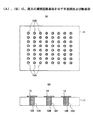
【0006】
図1(A),(B)は、かかる従来のビア形成基板の例を示すそれぞれ平面図および断面図である。
【0007】
図1(A)の平面図を参照するに、Al2O3等よりなるセラミック基板11中には多数のビアホール12Aが形成されており、各々のビアホール12AはCuあるいはWよりなるビアプラグ12Bにより充填されている。
【0008】
図1(A),(B)のビア形成基板は、主として配線基板と電子部品との間に挿入されて使われるように設計されており、各々のビアプラグ12Bに対応して図1(B)の断面図に示すようにNi等よりなる電極パッド13が形成されている。かかる電極パッド13上にはんだバンプを形成することにより、ビア形成基板は下側の配線基板と上側の部品とを電気的に接続する。
【0009】
図2は、かかるビア形成基板上に強誘電体キャパシタを含む薄膜回路を形成した本発明の関連技術によるインターポーザ型の薄膜回路基板の例を示す。かかる強誘電体キャパシタを搭載したインターポーザ型の薄膜回路基板では、LSIチップの直下に最短距離で電源配線を形成でき、電源ラインのインピーダンスが抑制される。その結果、かかるインターポーザ型の薄膜回路基板を使うことにより、クロック速度が非常に高い場合でも、LSIチップの高速動作に伴う電源電圧の変動を効果的に補償することが可能である。
【0010】
図2を参照するに、ビア形成基板11の上面においては図1(B)の電極パッド13が研磨処理により除去されており、さらにSBTやPZTなどの強誘電体材料あるいは高誘電体材料よりなるキャパシタ絶縁膜14が前記ビア形成基板11の上面に形成されている。前記キャパシタ絶縁膜14上には接地電極を構成する金属層15が形成されており、さらに前記金属層15上にはポリイミド保護膜16が形成されている。
【0011】
前記ポリイミド保護膜16中には前記金属層15およびキャパシタ絶縁膜14を貫通して前記ビアプラグ12Bの端面を露出するコンタクトホールが形成されており、前記コンタクトホールを充填するようにコンタクトプラグ17Aが形成されている。さらに前記ポリイミド保護膜16上には、前記コンタクトプラグ17Aの先端に結合して電極パッド17Bが形成されている。
【0012】
前記電極パッド17B上にははんだボール等のバンプ電極18が形成される。また、前記ビア形成基板11の下面では、前記電極パッド13上にばんだボール等のバンプ電極19が形成されている。
【0013】
【発明が解決しようとする課題】
このような強誘電体あるいは高誘電体よりなるキャパシタ絶縁膜を含む部品では、酸化雰囲気中、少なくとも700°C程度の高温での熱処理が必須であるが、ビアホール12A中のビアプラグ12Bは酸化しやすいCuあるいはWよりなるため、酸化の結果ビアプラグ12Bが膨張し、セラミック基板11表面に形成されている薄膜回路の破壊を引き起こしてしまうおそれもある。またセラミック基板は焼成工程により形成されるが、焼成に伴う収縮の制御が困難で、このためセラミック基板を使ったビア基板上に集積密度の大きいLSIを実装するのは困難である。
【0014】
これに対し、ビア形成基板としてSi基板を使い、半導体プロセスにより、かかるSi基板中に微細なビアホールを小さなピッチで形成することが考えられる。特にドライエッチングプロセスを使うことにより、Si基板中に非常に大きなアスペクト比の多数のビアホールを、非常に小さな繰り返しピッチで、しかも同時に形成することが可能である。
【0015】
一方、ドライエッチングプロセスでは、一般にエッチング速度がばらつきやすく、このため多数の深いビアホールをドライエッチングにより形成しようとした場合、深さ方向に±5%程度の加工誤差が生じるのが避けられない。その結果、所定時間のドライエッチングプロセスを終了した時点で、いくつかのビアホールは実際にはSi基板を貫通していない状態が出現する可能性がある。
【0016】
このような可能性に鑑み、Si基板に深いビアホールをドライエッチングにより形成する場合には、ドライエッチング工程の後で基板裏面を研磨し、ビアホールを確実に開口させる必要がある。またSi基板に深いビアホールをドライエッチングにより形成する場合には、ビアホール底部に針状の構造が形成されやすい。このようなことからも、前記研磨工程を行うのは不可欠であると考えられている。しかし、このような研磨工程は、ビア形成基板の費用を増大させてしまう。
【0017】
さらにこのようにして形成されたSi基板をベースとするビア形成基板では、ビアホールをCuやWなどの低抵抗金属で充填した後、余分の金属層を除去するためにさらなる研磨工程が必要であるが、その際に前記基板表面を、薄膜回路が形成できるように鏡面研磨する必要がある。しかし、このような鏡面研磨処理はビア形成基板の費用をさらに増大させてしまう。また、このようにして鏡面研磨されたビア形成基板の表面に、薄膜回路の形成に先立って絶縁膜を形成する工程が必要になる。
【0018】
さらにこのようにして形成されたSi基板をベースとするビア形成基板では、ビア形成基板上に強誘電体あるいは高誘電体キャパシタを含む薄膜回路を形成した場合、酸化雰囲気中での熱処理に伴ってビアホール中のビアプラグが酸化し、従来のセラミック基板をベースとするビア形成基板と同じ、薄膜回路の破壊ないし損傷の問題が発生してしまう。また、かかる強誘電体あるいは高誘電体キャパシタを含む薄膜回路を形成する際には、熱処理に伴ってビアプラグが収縮する場合もある。
【0019】
したがって、Si基板中にビアホールを形成したビア形成基板に基づいて、前記課題を解決した薄膜回路基板を提供することが要望されている。
【0020】
ところで、このようなビア形成基板を使ったMCM基板などのLSIを実装する基板では、LSIの集積密度の向上および機能の強化に伴って、ビアホールのピッチを減少させる必要がある。
【0021】
従来のセラミック基板を使ったビア形成基板あるいは樹脂基板を使ったビア形成基板では、ビアホールは機械加工により形成されているため、かかるピッチの減少には限界があったが、ビア形成基板として先に説明したようにSi基板を使い、ビアホールを半導体プロセスを使って形成することにより、これらの限界は打ち破ることが可能である。
【0022】
一方、このように非常に微細なビアホールを有するビア基板が実現されると、ビア基板上にLSI等の部品をはんだボールを介して実装した場合、部品実装時に、あるいはその後の電子装置の使用時に微細なはんだボールに非常に大きな応力が加わり、接合部の破損等の問題を引き起こす可能性がある。また、Si基板にビアホールをドライエッチング等の半導体プロセスで形成する場合には長時間のエッチングが必要になり、ビア形成基板の費用が増大してしまう。
【0023】
そこで、本発明は上記の課題を解決した、新規で有用な薄膜回路基板およびその製造方法、およびかかる薄膜回路基板を使った電子装置を提供することを概括的課題とする。
【0024】
本発明のより具体的な課題は、半導体基板を使ったビア形成基板をベースとする薄膜回路基板において、製造工程を簡素化でき、しかも形成される薄膜回路の信頼性を向上させることのできる薄膜回路基板およびその製造方法を提供することにある。
【0025】
本発明の他の課題は、半導体基板を使ったビア形成基板において、効率良く製造でき、ビア径およびビアピッチを減少させた場合でもバンプ電極に加わる応力を最小化できるビア形成基板およびその製造方法を提供することにある。
【0026】
【課題を解決するための手段】
本発明は上記の課題を、第1の主面と、前記第1の主面に対向する第2の主面とを有する半導体基板と、前記半導体基板上に、前記第1の主面に対応して形成された第1の絶縁膜と、前記半導体基板中を、前記第2の主面から前記第1の主面まで連続して延在するスルーホールと、前記スルーホールの側壁面を覆う第2の絶縁膜と、前記第1の絶縁膜上に形成された薄膜回路とよりなり、前記スルーホールは、前記第2の主面から延在する主部と、前記第1の主面近傍に形成されたテーパ部とよりなることを特徴とする薄膜回路基板により、または、薄膜回路基板の製造方法であって、第1および第2の主面により画成された半導体基板の前記第1の主面上にエッチング停止膜を形成する工程と、前記半導体基板の前記第2の主面上に、レジスト開口部を有するレジストパターンを形成する工程と、前記半導体基板に対し、前記レジストパターンをマスクにドライエッチングを行い、前記半導体基板中に、前記レジスト開口部に対応したスルーホールを、前記スルーホールにおいて前記エッチング停止膜が露出するように形成する工程と、前記スルーホールの側壁面に絶縁膜を形成する工程と、前記エッチング停止膜上に薄膜回路を形成する工程と、前記スルーホールにおいて前記エッチング停止膜を除去し、前記薄膜回路を露出する開口部を形成する工程とよりなることを特徴とする薄膜回路基板の製造方法により解決する。
【0027】
本発明によれば、薄膜回路が、あらかじめ鏡面仕上げされている半導体基板表面上に、ビアプラグ形成工程よりも前に形成されるため、従来必要とされていた、ビアプラグ形成工程後の鏡面研磨工程が省略でき、薄膜回路基板の製造工程が簡素化される。また本発明によれば、薄膜回路がビアプラグ形成工程よりも前に形成されるため、薄膜回路形成工程に強誘電体膜や高誘電体膜の酸化熱処理工程が含まれていても、ビアプラグが酸化したり膨張・収縮することがなく、薄膜回路基板の製造歩留りを向上させることができる。さらにSi基板等の半導体基板を使い、スルーホールをドライエッチング工程により形成することにより、容易にビア径を微細化し、またビアピッチを微細化することができる。
【0028】
ところで、スルーホールをこのようにドライエッチングにより形成する際に、本発明はオーパーエッチングを行うことにより、基板中の全てのスルーホールを確実に貫通させることができる。かかるオーバーエッチングを行うと、スルーホールの底部が側方に拡大する傾向が現れるが、本発明はスルーホールの側方への拡大を抑制するため、基板底面にスルーホールを囲むように酸化膜を形成する。このような構成では、前記スルーホールを形成するドライエッチングプロセスが基板底面のエッチング停止膜により阻止された場合、ドライエッチングプロセスの側方へ進行が前記酸化膜により阻止される。このため、スルーホール底部の拡大が抑制され、微細なスルーホールを微細なピッチで繰り返し形成することが可能になる。
【0029】
本発明はまた、上記の課題を、第1の主面と前記第1の主面に対向する第2の主面とよりなる支持基板と、前記支持基板中に、前記第2の主面から前記第1の主面に向って第1の径で延在するようにスルーホールと、前記スルーホールの前記第1の主面側端部に形成され、前記第1の主面において開口し、径を前記第1の主面に向って前記第1の径から増大させ、前記第1の主面において前記第1の径よりも大きな第2の径を有するテーパ形状部と、前記スルーホールを充填する導体プラグと、前記テーパ形状部上に、前記導体プラグに電気的に接続されて形成された、前記テーパ形状部に対応するテーパ形状を有するパッド電極とよりなることを特徴とするビア形成基板により、または、半導体基板の第1の主面上に、異方性エッチングにより、テーパ状の凹部を形成する工程と、前記テーパ状凹部の表面を覆うように、前記テーパ状凹部に対応した形状の絶縁膜を形成する工程と、前記半導体基板中に、前記第1の主面に対向する第2の主面から前記第1の主面に向って延在するビアホールを、前記テーパ状凹部に対応して、前記ビアホールが前記テーパ状凹部において前記絶縁膜を露出するように形成する工程と、前記テーパ状凹部を覆う前記絶縁膜上にパッド電極を、前記テーパ上凹部に対応した形状に形成する工程と、前記ビアホール底部において、前記露出している絶縁膜を除去し、前記パッド電極を露出する工程と、前記ビアホールを導体により充填してビアプラグを形成する工程とよりなることを特徴とするビア形成基板の形成方法により、解決する。
【0030】
本発明によれば、ビア基板中のビアホール端部にテーパ形状部を形成することにより、微細なビアホールであってもその上に比較的径の大きなはんだボールないしバンプ電極を形成することが可能になる。その結果、かかるビア基板上にLSIチップ等の部品を実装した場合に、バンプ電極に加わる応力を緩和することが可能になる。本発明は、特にSi基板等の半導体基板中に非常に微細なビアホールを非常に微細なピッチで形成したビア基板において有効である。かかるテーパ形状部は、予め半導体基板表面にウェットエッチング等の異方性エッチングにより形成しておくことができる。このようにテーパ形状部を予め形成したおいた場合、スルーホールを形成するドライエッチング工程を短縮することが可能になり、ビア形成基板の製造効率を向上させることができる。
【0031】
【発明の実施の形態】
[第1実施例]
図3(A)〜(E)は、本発明の第1実施例による薄膜回路基板20の製造工程を示す。
【0032】
図3(A)を参照するに、厚さが300〜600μmの単結晶Si基板21の下主面面にはSiO2膜よりなるエッチング停止膜22がCVD工程により、約2μmの厚さに形成される。
【0033】
次に図3(B)の工程において前記Si基板21の上主面に、数十μmの径のレジスト開口部23Aが形成されたレジストパターン23を形成し、図3(C)の工程においてICPプラズマエッチング装置中において、前記レジストパターン23をマスクに前記Si基板21の露出部に、C4F8およびSF6エッチングガスを交互に供給することにより、ドライエッチングを約180分間行い、前記Si基板21中を前記上主面から下主面まで延在するスルーホール21Aが形成される。前記スルーホール21Aを形成するドライエッチングは、前記スルーホール21Aにおいてエッチング停止膜22が露出した時点で停止する。
【0034】
図3(C)の工程では、同時に多数のスルーホール21Aが形成されるが、スルーホールごとのエッチング速度のばらつきに鑑み、全てのスルーホール21Aが前記上主面から下主面まで貫通するように、エッチングを多少長く実行し、オーバーエッチングを行う。かかるオーバーエッチングの結果、前記スルーホール21Aは大部分垂直な壁面で画成されるものの、前記エッチング停止膜22に接する底部においては、深さが約10μmの範囲で径が約10μm程度拡大し、オーバーエッチ部21Bが形成される。図3(C)よりわかるように、かかるオーバーエッチ部21Bにおいて前記エッチング停止膜22が露出している。
【0035】
次に図3(D)の工程で前記レジストパターン23が除去され、さらに800〜1050°Cの温度で熱酸化処理工程を行うことにより、あるいはCVD工程を行うことにより、前記スルーホール21Aの内壁面に、前記オーバーエッチ部21Bも含めて、酸化膜21Cが形成される。また、図3(D)の工程では、前記エッチング停止膜22上に薄膜回路24が形成されている。かかる薄膜回路24は、先に図2に示したような、強誘電体キャパシタあるいは高誘電体キャパシタを含むものであってもよい。あるいは、かかる薄膜回路24は多層配線構造であってもよい。前記薄膜回路24が強誘電体キャパシタあるいは高誘電体キャパシタを含む場合、図3(D)の工程においては酸化雰囲気中600〜800°Cでの熱処理が行われ、形成された強誘電体膜あるいは高誘電体膜中の酸素欠損補償処理が行われる。
【0036】
次に図3(E)の工程において前記エッチング停止膜22が、前記スルーホール21Aを介したドライエッチングにより除去され、前記エッチング停止膜22中には、前記スルーホール21Aに対応した開口部が形成され、かかる開口部において前記薄膜回路24が露出される。
【0037】
図3(E)の構造では、前記エッチング停止膜22はSi基板21の下主面に対応したスルーホール21A下端部からスルーホール中心部に向って、前記側壁酸化膜21Cの厚さに対応する距離だけ延在しており、前記側壁酸化膜21Cは、その端面がかかるエッチング停止膜22の延在部の上面に接合している。
【0038】
前記側壁酸化膜21Cと前記エッチング停止膜22とが共に酸化膜である場合、図3(E)のドライエッチングでは膜21Cと22との間に実質的なエッチング選択性は確保できないので、エッチング停止膜22のみが確実に除去されるように、前記側壁酸化膜21Cの膜厚を、前記エッチング停止膜22の膜厚よりも大きく設定しておくのが好ましい。
【0039】
図4は、このようにして形成された薄膜回路基板20中にビアプラグを形成し、さらにはんだバンプを形成した構成を示す。
【0040】
図4を参照するに、前記スルーホール21A中には、前記スルーホール21Aを充填するようにCuやW等の低抵抗金属よりなるビアプラグ21Dが形成されており、前記ビアプラグ21Dの上端にはPtあるいはAu等よりなるパッド電極21Eが形成されている。
【0041】
一方、前記薄膜回路24上にも前記ビアプラグ21Dに対応してパッド電極21Fが形成されており、前記パッド電極21F上にははんだボール25よりなるバンプ電極が形成されている。
【0042】
図4の構成の薄膜回路基板20では、前記ビアプラグ21Dを形成する以前に薄膜回路24が形成されているため、ビアプラグ21Dを形成した後で高温酸化雰囲気中で熱処理を行う必要がなく、ビアプラグ21Dの酸化による膨張およびこれに伴い薄膜回路24の破壊の問題が生じない。
【0043】
また図4の構成の薄膜回路基板20では、Si基板を使うことにより、図1(A),(B)のセラミック基板を使う場合のような既存の電極パッドを研磨により除去する工程が不必要で、さらに前記スルーホール21A、従ってビアプラグ21Dを非常に小さな径で、しかも非常に小さな繰り返しピッチで形成することが可能になる。
[第2実施例]
図5(A)〜図6(F)は、本発明の第2実施例による薄膜回路基板20Aの製造方法を示す。ただし図中、先に説明した部分には同一の参照符号を付し、説明を省略する。
【0044】
図5(A)を参照するに、Si基板21の下主面上にはエッチング停止膜となるSiNパターン31が、形成しようとうするビアホールに対応して形成され、図5(B)の工程において図5(A)のSi基板21に対して熱酸化処理工程を行う。その結果、図5(B)に示すように前記Si基板21の下主面には、前記SiNパターン31の両側に熱酸化膜31が、自己整合的に形成される。
【0045】
次に図5(C)の工程において前記Si基板21の上主面上に、形成しようとするビアホールに対応したレジスト開口部23Aを有するレジスト膜23が、図3(B)の工程と同様にして形成され、図5(C)の工程において前記レジスト膜23をマスクに、前記Si基板21を、前記SiNエッチング停止パターン31が露出するまでドライエッチングし、前記Si基板21中に、前記レジスト開口部21に対応してスルーホール21Aを形成する。先の実施例と同様に、前記スルーホール21Aを形成するドライエッチング工程では、前記Si基板11中の全てのスルーホール21Aにおいて前記SiNエッチング停止パターン31が確実に露出されるように、エッチング時間を延長し、いわゆるオーバーエッチングを行う。
【0046】
さらに図6(E)の工程において前記レジスト膜23が除去され、図6(D)の工程で形成されたスルーホール21Aの内壁面に、熱酸化工程あるいはCVD工程により、絶縁膜21Cが形成される。また図6(E)の工程においては、前記Si基板21の下主面上の熱酸化膜32上に薄膜回路24が形成される。前記薄膜回路24は、先に説明したように強誘電体膜あるいは高誘電体膜を含むものであってもよく、その場合には結晶化および酸素欠損補償のための酸化雰囲気中における熱処理が行われる。
【0047】
さらに図6(F)の工程において前記SiNエッチングパターン31が選択エッチング工程により除去され、前記薄膜回路が露出される。
【0048】
図6(F)の工程の後、前記ビアホール21AをCuやWにより充填することにより、図4と略同様な薄膜回路基板20Aが得られる。
【0049】
本実施例では、図5(B)の工程において前記Si基板21の下主面上に前記SiNエッチング停止パターン31に自己整合して熱酸化膜32を形成しているため、図6(F)の選択エッチングにより、側壁の絶縁層は確保され、確実に開口部をエッチングできる利点がある。
[第3実施例]
図7は、本発明の第3実施例によるビア形成基板40の構成を示す。
【0050】
図7を参照するに、ビア形成基板40は厚さが数百ミクロンのSi基板41をベースに構成されており、前記Si基板41と、前記Si基板41の上主面に形成された複数の凹部42と、前記凹部の各々に対応して形成され、前記凹部の底部から前記Si基板41の下主面まで、前記Si基板41中を貫通するスルーホール43とよりなり、前記Si基板41の上下主面、前記凹部表面、前記スルーホール内壁面および前記Si基板41の側壁面は、好ましくは熱酸化膜よりなる絶縁膜41aにより覆われている。
【0051】
前記凹部42は好ましくはSiの結晶面により画成されており、Pt等よりなる電極パッド42Aが、前記凹部42の凹面形状に対応して形成されている。また、前記スルーホール43はPtよりなるビアプラグ43Aにより充填されている。前記Si基板41の下主面上には、前記ビアプラグ43Aの各々に対応して、Pt等よりなる電極パッド43Bが形成されている。
【0052】
図示の例では前記スルーホール43は70μmの深さを有し、前記Si基板41中に250μmピッチで繰り返し形成されている。また前記凹部42はSiの(111)面により画成されており、前記Si基板41の上主面において径が約140μmの開口部を形成する。
【0053】
前記各々のスルーホール43は対応する凹部42とともに、前記Si基板41中を、前記上主面側から下主面側まで連続して延在するビアホールを形成する。
【0054】
前記凹部42の各々は、前記電極パッド42Aにコンタクトする半田プラグ44により充填され、前記半田プラグ44の先端部には、径が約150μmの半田ボール44Aが形成されている。
【0055】
図7の構成では、かかるビア基板上にパッド電極52を有するLSI基板52が実装されており、前記パッド電極52の各々が、対応する半田ボール44Aとコンタクトする。
【0056】
かかる構成では、前記Si基板41の表面に凹部42を形成しておくことにより、前記スルーホール43、従ってビアホールの形成ピッチ自体は非常に小さくても、前記凹部42に対応して比較的大きな径の半田ボール44Aを形成することが可能になる。このような大きな半田ボール44Aを使うことにより、前記LSI基板52に外力が加わったような場合でも、半田ボール44Aおよび半田プラグ44に印加される応力は小さく、コンタクト部の破損等の問題を回避することが可能になる。また、このように凹部42を形成することにより、LSI基板51の実装時に生じる熱応力も、軽減される。
【0057】
本発明では、Si基板41の代わりに他の基板を使うことも可能であるが、ウエットエッチング等の異方性エッチングにより凹部42を正確に形成できることから、前記基板41としてはSi基板をはじめとする半導体基板を使うのが好ましい。
【0058】
なお、図7中に示した数値はあくまでも例示のためのものであり、本発明を限定するものではない。また前記LSI基板の代わりにLSIチップを実装することも可能である。
【0059】
次に、図7のビア形成基板の製造工程を、図8(A)〜図9(M)を参照しながら説明する。
【0060】
図8(A)を参照するに、前記Si基板41の(100)表面に熱酸化工程により酸化膜41aが形成される。
【0061】
次に図8(B)の工程において前記Si基板41の上主面上の酸化膜41aがフォトリソグラフィー法によりパターニングされ、形成された開口部において前記Si基板41をKOHを使ったウェットエッチング法により異方性エッチングを行うことにより、前記Si基板41の上主面にSi(111)面により画成された凹部42を繰り返し形成する。
【0062】
次に図8(C)の工程において、図8(B)の工程で形成された凹部42の表面に再び熱酸化膜41aを形成し、さらに図8(D)の工程において前記Si基板41の下主面上の酸化膜41a中に、前記Si基板41の下主面を露出するように、開口部41bを、前記凹部42の各々に対応して形成する。
【0063】
次に図8(E)の工程において、図8(D)のSi基板41をICP型ドライエッチング装置(図示せず)の反応室に導入し、C4F8およびSF6をエッチングガスとしたドライエッチング工程を行うことにより、前記開口部41bの各々に対応して開口部43が、前記Si基板41の下主面から上主面に向って延在するように形成される。図8(E)に示すようにドライエッチング工程は、前記凹部42の底面を覆っている酸化膜41aが露出した時点で停止する。
【0064】
次に図8(F)の工程において図8(E)の構造に対して熱酸化工程が行われ、前記開口部43の側壁面に熱酸化膜が形成される。
【0065】
さらに図8(G)の工程において、図8(F)の構造上にPt膜等の導電膜が堆積され、これをパターニングすることにより、前記凹部42上に前記電極パッド42Aが形成される。
【0066】
次に図9(H)の工程において、図8(F)の構造において前記電極パッド42Aと開口部43との間に介在していた熱酸化膜41aがドライエッチング工程により除去され、前記開口部43の上端部において前記電極パッド42Aが露出する。すなわち、図9(H)の段階において、前記開口部43はSi基板41中を延在するスルーホールとなる。
【0067】
次に図9(I)の工程において前記スルーホール43の各々にビアプラグ43Aが電解めっき等の工程により形成され、さらに前記Si基板41の下面上に、前記ビアプラグ43Aに対応してPt等よりなる電極パッド43Bが形成されている。
【0068】
次に図9(J)の工程において、前記電極パッド42Aの各々の上にSn−Ag系の半田ペースト43aをリフトオフ法等により塗布し、さらに熱処理を260°Cで行うことにより塗布された半田をリフローさせ、ビア形成基板を形成する。
【0069】
さらに図9(K)の工程において前記半田ペースト43a上に径が150〜180μmの半田ボール44Aを転写し、図9(L)の工程において、図9(J)のビア形成基板上にLSI基板51を、前記半田ボール44Aを介して実装する。
【0070】
さらに図9(M)の工程において、図9(L)のビア形成基板を、配線基板61上に、前記電極パッド43Bおよび半田バンプ45を介して実装することにより、電子装置を形成する。
【0071】
本実施例では、先にも説明したように前記ビア形成基板の表面に凹部42を形成しておくことにより大きな径の半田ボールを使うことが可能で、このため前記LSI基板51に対して外力が加わっても、前記半田ボールに印加される応力を効果的に分散させることができ、損傷を回避することが可能になる。
【0072】
また本実施例では、前記Si基板上に予めウェットエッチング工程等の異方性エッチング工程により予め凹部42が形成されるため、スルーホール43Aを形成する際のドライエッチング工程が短時間で済む好ましい特徴が得られる。
【0073】
なお、本発明の薄膜回路基板20,20Aあるいはビア形成基板40は、図9(M)で説明したインターポーザ型基板のみならず、図10に示すように配線基板61上にバンプ電極により実装し、さらにリード線62で配線を行うことによりシステムパッケージを形成するのに使うことも可能である。
【0074】
さらに本発明の薄膜回路基板20,20Aあるいはビア形成基板40は、図11に示すようにFRAMやCMOSの集積回路装置を担持することにより、システムインパッケージを形成することも可能である。
【0075】
さらに本発明の薄膜回路基板20,20Aあるいはビア形成基板40は、図9(M)の実装構造を積層することにより、3次元集積回路装置を構成することも可能である。
【0076】
以上、本発明を好ましい実施例について説明したが、本発明はかかる特定の構成に限定されるものではなく、特許請求の範囲内において様々な変形・変更が可能である。
【0077】
(付記1) 第1の主面と、前記第1の主面に対向する第2の主面とを有する半導体基板と、
前記半導体基板上に、前記第1の主面に対応して形成された第1の絶縁膜と、
前記半導体基板中を、前記第2の主面から前記第1の主面まで連続して延在するスルーホールと、
前記スルーホールの側壁面を覆う第2の絶縁膜と、
前記第1の絶縁膜上に形成された薄膜回路とよりなり、
前記スルーホールは、前記第2の主面から延在し実質的に一定の第1の径を有する主部と、前記第1の主面近傍に形成され、前記第1の径よりも大きな第2の径を有するテーパ部とよりなることを特徴とする薄膜回路基板。
【0078】
(付記2) 前記第1の絶縁膜には、前記スルーホール中において、前記第2の絶縁膜の内壁面により画成される開口部が形成されていることを特徴とする付記1記載の薄膜回路基板。
【0079】
(付記3) 前記第1の絶縁膜は、前記開口部において、前記スルーホールの側壁面から前記第2の絶縁膜の厚さに対応する距離だけ前記開口部中央に向って延在し、前記第2の主面に一致する側壁面と前記開口部に一致する端面とにより画成される延在部を有し、前記第2の絶縁膜は、前記延在部の前記側壁面に衝合することを特徴とする付記2記載の薄膜回路基板。
【0080】
(付記4) 前記薄膜回路は、前記第1の絶縁膜と接する側が平坦面を形成することを特徴とする付記1〜3のうち、いずれか一項記載の薄膜回路基板。
【0081】
(付記5) 前記薄膜回路には、前記スルーホールに対応して、前記第1の絶縁膜に接する側に、前記開口部よりも大きな径の凹部が形成されていることを特徴とする付記2または3記載の薄膜回路基板。
【0082】
(付記6) 前記薄膜回路と前記第1の絶縁膜との間には、前記スルーホールに対応して、前記開口部前記開口部よりも大きな径を有する絶縁膜パターンが形成されていることを特徴とする付記2または3記載の薄膜回路基板。
【0083】
(付記7) 前記第2の絶縁膜の厚さは、前記第1の絶縁膜の厚さよりも大きいことを特徴とする付記1〜6のうち、いずれか一項記載の薄膜回路基板。
【0084】
(付記8) 前記スルーホールは、導電体により充填されていることを特徴とする付記1〜7のうち、いずれか一項記載の薄膜回路装置。
【0085】
(付記9) 前記薄膜回路は強誘電体膜あるいは高誘電体膜を含むことを特徴とする付記1〜8のうち、いずれか一項記載の薄膜回路基板。
【0086】
(付記10) 前記第1および第2の絶縁膜は酸化膜よりなることを特徴とする付記1〜9のうち、いずれか一項記載の薄膜回路基板。
【0087】
(付記11) 薄膜回路基板の製造方法であって、
第1および第2の主面により画成された半導体基板の前記第1の主面上にエッチング停止膜を形成する工程と、
前記半導体基板の前記第2の主面上に、レジスト開口部を有するレジストパターンを形成する工程と、
前記半導体基板に対し、前記レジストパターンをマスクにドライエッチングを行い、前記半導体基板中に、前記レジスト開口部に対応したスルーホールを、前記スルーホールにおいて前記エッチング停止膜が露出するように形成する工程と、
前記スルーホールの側壁面に絶縁膜を形成する工程と、
前記エッチング停止膜上に薄膜回路を形成する工程と、
前記スルーホールにおいて前記エッチング停止膜を除去し、前記薄膜回路を露出する開口部を形成する工程とよりなることを特徴とする薄膜回路基板の製造方法。
【0088】
(付記12) 前記スルーホールを形成する工程は、前記エッチング停止膜が露出した後、前記ドライエッチングをさらに継続するオーバーエッチング工程を含むことを特徴とする付記11記載の薄膜回路基板の製造方法。
【0089】
(付記13) 前記エッチング停止膜を形成する工程は、前記第1の主面上に、前記第1の主面上において前記スルーホール形成領域を覆う絶縁膜パターンを、前記エッチング停止膜として形成する工程と、前記絶縁膜パターンをマスクに、前記半導体基板の前記第1の主面を酸化して、前記絶縁膜パターンの周囲に酸化膜を形成する工程とを含み、
前記酸化膜は、前記オーバーエッチング工程において、オーバーエッチング停止膜として作用することを特徴とする付記12記載の薄膜回路基板の製造方法。
【0090】
(付記14) 前記エッチング停止膜はSiN膜またはSiO2膜よりなることを特徴とする付記11〜13のうち、いずれか一項記載の薄膜回路基板の製造方法。
【0091】
(付記15) 前記薄膜回路は強誘電体膜あるいは高誘電体膜を含み、前記薄膜回路を形成する工程は、酸化雰囲気中での熱処理工程を含むことを特徴とする付記11〜14のうち、いずれか一項記載の薄膜回路基板の製造方法。
【0092】
(付記16) 前記エッチング停止膜除去工程の後、前記前記スルーホールに導体を充填する工程をさらに含むことを特徴とする付記11〜15のうち、いずれか一項記載の薄膜回路基板の製造方法。
【0093】
(付記17) 第1の主面と前記第1の主面に対向する第2の主面とよりなる支持基板と、
前記支持基板中に、前記第2の主面から前記第1の主面に向って第1の径で延在するようにスルーホールと、
前記スルーホールの前記第1の主面側端部に形成され、前記第1の主面において開口し、径を前記第1の主面に向って前記第1の径から増大させ、前記第1の主面において前記第1の径よりも大きな第2の径を有するテーパ形状部と、
前記スルーホールを充填する導体プラグと、
前記テーパ形状部上に、前記導体プラグに電気的に接続されて形成された、前記テーパ形状部に対応するテーパ形状を有するパッド電極とよりなることを特徴とするビア形成基板。
【0094】
(付記18) 前記パッド電極上にバンプ電極をさらに有することを特徴とする付記17記載のビア形成基板。
【0095】
(付記19) 前記基板はSi基板よりなることを特徴とする付記17または18記載のビア形成基板。
【0096】
(付記20) 前記テーパ形状部は、Si結晶面により画成されていることを特徴とする付記19記載のビア形成基板。
【0097】
(付記21) 前記第2の径は、前記第1の径よりも二倍以上大きいことを特徴とする付記17〜20のうち、いずれか一項記載のビア形成基板。
【0098】
(付記22) 前記基板上には薄膜回路が形成されていることを特徴とする付記17〜21のうち、いずれか一項記載のビア形成基板。
【0099】
(付記23) 半導体基板の第1の主面上に、異方性エッチングにより、テーパ状の凹部を形成する工程と、
前記テーパ状凹部の表面を覆うように、前記テーパ状凹部に対応した形状の絶縁膜を形成する工程と、
前記半導体基板中に、前記第1の主面に対向する第2の主面から前記第1の主面に向って延在するビアホールを、前記テーパ状凹部に対応して、前記ビアホールが前記テーパ状凹部において前記絶縁膜を露出するように形成する工程と、
前記テーパ状凹部を覆う前記絶縁膜上にパッド電極を、前記テーパ上凹部に対応した形状に形成する工程と、
前記ビアホール底部において、前記露出している絶縁膜を除去し、前記パッド電極を露出する工程と、
前記ビアホールを導体により充填してビアプラグを形成する工程とよりなることを特徴とするビア形成基板の形成方法。
【0100】
(付記24) 前記半導体基板はSi基板よりなり、前記異方性エッチング工程は、ウェットエッチングにより実行されることを特徴とする付記23記載のビア形成基板の形成方法。
【0101】
(付記25) 前記ビアホール形成工程は、ドライエッチングにより実行されることを特徴とする付記23または24記載のビア形成基板の形成方法。
【0102】
(付記26) 前記ビアプラグ形成工程は、前記導体のめっき工程を含むことを特徴とする付記23〜25のうち、いずれか一項記載のビア形成基板の形成方法。
【0103】
(付記27) 前記導体はPtまたはAuよりなることを特徴とする付記23〜26のうち、いずれか一項記載のビア形成基板の形成方法。
【0104】
(付記28) さらに、前記電極パッド上にはんだペーストを形成する工程と、前記はんだペースト上にはんだボールを設ける工程とを含むことを特徴とする付記23〜27のうち、いずれか一項記載のビア形成基板の形成方法。
【0105】
(付記29) さらに前記はんだボールを加熱することにより、前記電極パッド上にバンプ電極を形成する工程を含むことを特徴とする付記28記載のビア形成基板の形成方法。
【0106】
【発明の効果】
本発明によれば、薄膜回路があらかじめ鏡面仕上げされている半導体基板表面上に、ビアプラグ形成工程よりも前に形成されるため、従来必要とされていた、ビアプラグ形成工程後の鏡面研磨工程が省略でき、薄膜回路基板の製造工程が簡素化される。また本発明によれば、薄膜回路がビアプラグ形成工程よりも前に形成されるため、薄膜回路形成工程に強誘電体膜や高誘電体膜の酸化熱処理工程が含まれていても、ビアプラグが酸化したり膨張・収縮することがなく、薄膜回路基板の製造歩留りを向上させることができる。さらにSi基板等の半導体基板を使い、スルーホールをドライエッチング工程により形成することにより、容易にビア径を微細化し、またビアピッチを微細化することができる。
【0107】
本発明によれば、ビア基板中のビアホール端部にテーパ形状部を形成することにより、微細なビアホールであってもその上に比較的径の大きなはんだボールないしバンプ電極を形成することが可能になる。その結果、かかるビア基板上にLSIチップ等の部品を実装した場合に、バンプ電極に加わる応力を緩和することが可能になる。本発明は、特にSi基板等の半導体基板中に非常に微細なビアホールを非常に微細なピッチで形成したビア基板において有効である。かかるテーパ形状部は、予め半導体基板表面にウェットエッチング等の異方性エッチングにより形成しておくことができる。このようにテーパ形状部を予め形成したおいた場合、スルーホールを形成するドライエッチング工程を短縮することが可能になり、ビア形成基板の製造効率を向上させることができる。
【図面の簡単な説明】
【図1】(A),(B)は、従来の薄膜回路基板を示す平面図および断面図である。
【図2】図1の薄膜回路基板を示す拡大断面図である。
【図3】(A)〜(E)は、本発明の第1実施例による薄膜回路基板の製造工程を示す図である。
【図4】本発明の第1実施例による薄膜回路基板の構成を示す断面図である。
【図5】(A)〜(C)は、本発明の第2実施例による薄膜回路基板の製造工程を示す図(その1)である。
【図6】(D)〜(F)は、本発明の第2実施例による薄膜回路基板の製造工程を示す図(その2)である。
【図7】本発明の第3実施例によるビア形成基板の構成を示す図である。
【図8】(A)〜(G)は、図7のビア形成基板の製造工程を示す図(その1)である。
【図9】(H)〜(M)は、図7のビア形成基板の製造工程を示す図(その2)である。
【図10】本発明の薄膜回路基板あるいはビア形成基板により構成されるシステムパッケージの例を示す図である。
【図11】本発明の薄膜回路基板あるいはビア形成基板により構成されるシステムインパッケージの例を示す図である。
【符号の説明】
11 セラミック基板
12A ビアホール
12B ビアプラグ
13 電極パッド
14 強誘電体・高誘電体膜
15 接地電極層
16 ポリイミド保護膜
17A コンタクトプラグ
17B 電極パッド
18,19 半田ボール
20,21A 薄膜回路基板
21 Si基板
21A スルーホール
21B スルーホール底部
21C 絶縁膜
21D ビアプラグ
21E,21F 電極パッド
22 エッチング停止膜
23 レジスト膜
23A レジスト開口部
24 薄膜回路
25 半田ボール
31 SiNパターン
32 熱酸化膜
40 ビア形成基板
41 Si基板
42 凹部
42A 絶縁膜
43 スルーホール
43A ビアプラグ
43B 電極パッド
44A 半田プラグ
44B 半田ボール
51 LSI基板
61 回路基板[0001]
BACKGROUND OF THE INVENTION
The present invention generally relates to electronic devices, and more particularly to a thin film circuit board having a through hole and a method for manufacturing the same.
[0002]
A so-called via-formed substrate in which a large number of through holes are formed is an important component in interposer-type components, multilayer circuit boards, and three-dimensional chip mounting technology.
[0003]
Various wiring patterns are formed on the via-formed substrate. Particularly in the case of an interposer type component inserted between the wiring substrate and the LSI chip, a high dielectric capacitor or a ferroelectric capacitor is formed on the substrate. As a result, it is possible to absorb fluctuations in the power supply voltage due to high-speed operation of the LSI chip.
[0004]
Furthermore, it is possible to form a system package by forming such a via formation substrate together with other components on a package substrate, and by disposing various components including LSI chips on the via formation substrate. A multi-chip module (MCM) or system-in-package can be formed.
[0005]
[Prior art]
Conventionally, via formation substrates based on ceramic substrates are commercially available. In such a commercially available via forming substrate, a large number of through holes are formed in a ceramic substrate, and a via plug made of a low resistance metal such as Cu or W is embedded in each through hole.
[0006]
1A and 1B are a plan view and a cross-sectional view, respectively, showing an example of such a conventional via forming substrate.
[0007]
Referring to the plan view of FIG. 2 O Three A large number of
[0008]
The via formation substrate of FIGS. 1A and 1B is designed to be used by being inserted mainly between a wiring substrate and an electronic component. FIG. 1B corresponds to each via
[0009]
FIG. 2 shows an example of an interposer type thin film circuit substrate according to the related art of the present invention in which a thin film circuit including a ferroelectric capacitor is formed on such a via formation substrate. In an interposer type thin film circuit board on which such a ferroelectric capacitor is mounted, power supply wiring can be formed at the shortest distance directly under the LSI chip, and impedance of the power supply line is suppressed. As a result, by using such an interposer-type thin film circuit board, even when the clock speed is very high, it is possible to effectively compensate for fluctuations in the power supply voltage accompanying the high-speed operation of the LSI chip.
[0010]
Referring to FIG. 2, the
[0011]
A contact hole is formed in the polyimide protective film 16 so as to penetrate the
[0012]
[0013]
[Problems to be solved by the invention]
In a part including a capacitor insulating film made of such a ferroelectric or high dielectric, heat treatment at a high temperature of at least about 700 ° C. is essential in an oxidizing atmosphere, but the
[0014]
On the other hand, it is conceivable to use a Si substrate as a via formation substrate and form fine via holes at a small pitch in the Si substrate by a semiconductor process. In particular, by using a dry etching process, a large number of via holes having a very large aspect ratio can be formed in a Si substrate at a very small repetition pitch and at the same time.
[0015]
On the other hand, in the dry etching process, the etching rate generally tends to vary. For this reason, when many deep via holes are to be formed by dry etching, it is inevitable that a processing error of about ± 5% occurs in the depth direction. As a result, when the dry etching process for a predetermined time is finished, there is a possibility that some via holes may not actually penetrate the Si substrate.
[0016]
In view of such a possibility, when a deep via hole is formed in a Si substrate by dry etching, it is necessary to polish the back surface of the substrate after the dry etching step to reliably open the via hole. Further, when a deep via hole is formed in the Si substrate by dry etching, a needle-like structure is easily formed at the bottom of the via hole. From this point of view, it is considered indispensable to perform the polishing step. However, such a polishing process increases the cost of the via-formed substrate.
[0017]
Further, in the via formation substrate based on the Si substrate formed in this way, after the via hole is filled with a low resistance metal such as Cu or W, an additional polishing step is required to remove the excess metal layer. However, the substrate surface needs to be mirror-polished so that a thin film circuit can be formed. However, such a mirror polishing process further increases the cost of the via-formed substrate. In addition, a process for forming an insulating film on the surface of the via forming substrate thus mirror-polished prior to the formation of the thin film circuit is required.
[0018]
Furthermore, in the via formation substrate based on the Si substrate formed in this way, when a thin film circuit including a ferroelectric or high dielectric capacitor is formed on the via formation substrate, the heat treatment in an oxidizing atmosphere is accompanied. The via plug in the via hole is oxidized, and the same problem of destruction or damage of the thin film circuit as in the conventional via formation substrate based on the ceramic substrate occurs. Further, when forming a thin film circuit including such a ferroelectric or high dielectric capacitor, the via plug may shrink with heat treatment.
[0019]
Therefore, it is desired to provide a thin film circuit board that solves the above problems based on a via-formed substrate in which a via hole is formed in an Si substrate.
[0020]
By the way, in a substrate on which an LSI such as an MCM substrate using such a via formation substrate is mounted, it is necessary to reduce the pitch of the via holes as the integration density of the LSI is improved and the function is enhanced.
[0021]
In a via formation substrate using a conventional ceramic substrate or a via formation substrate using a resin substrate, the via hole is formed by machining, so there was a limit in reducing the pitch. As described, these limitations can be overcome by using a Si substrate and forming via holes using a semiconductor process.
[0022]
On the other hand, when a via substrate having such a very fine via hole is realized, when a component such as an LSI is mounted on the via substrate via a solder ball, when mounting the component, or when using an electronic device thereafter A very large stress is applied to the fine solder balls, which may cause problems such as breakage of the joints. In addition, when a via hole is formed in a Si substrate by a semiconductor process such as dry etching, long-time etching is required, and the cost of the via formation substrate increases.
[0023]
SUMMARY OF THE INVENTION Accordingly, it is a general object of the present invention to provide a novel and useful thin film circuit board and a method for manufacturing the same, and an electronic device using such a thin film circuit board, which have solved the above problems.
[0024]
A more specific object of the present invention is a thin film circuit that can simplify the manufacturing process and improve the reliability of the formed thin film circuit in a thin film circuit board based on a via forming substrate using a semiconductor substrate. A circuit board and a manufacturing method thereof are provided.
[0025]
Another object of the present invention is to provide a via forming substrate that can be efficiently manufactured in a via forming substrate using a semiconductor substrate, and can minimize the stress applied to the bump electrode even when the via diameter and the via pitch are reduced, and a manufacturing method thereof. It is to provide.
[0026]
[Means for Solving the Problems]
The present invention addresses the above-described problem by providing a semiconductor substrate having a first main surface and a second main surface opposite to the first main surface, and the first main surface on the semiconductor substrate. A first insulating film formed in this manner, a through hole continuously extending from the second main surface to the first main surface in the semiconductor substrate, and a side wall surface of the through hole. The through-hole includes a main portion extending from the second main surface, and the vicinity of the first main surface. The second insulating film includes a second insulating film and a thin film circuit formed on the first insulating film. A thin film circuit board, or a method of manufacturing a thin film circuit board, wherein the first of the semiconductor substrates defined by the first and second main surfaces Forming an etching stop film on the main surface of the semiconductor substrate, and forming a resist on the second main surface of the semiconductor substrate. Forming a resist pattern having a trench opening, and performing dry etching on the semiconductor substrate using the resist pattern as a mask to form a through hole corresponding to the resist opening in the semiconductor substrate. Forming an etching stop film so as to be exposed, forming an insulating film on a sidewall surface of the through hole, forming a thin film circuit on the etching stop film, and etching the through hole The problem is solved by a method of manufacturing a thin film circuit substrate, comprising the step of removing the stop film and forming an opening exposing the thin film circuit.
[0027]
According to the present invention, since the thin film circuit is formed on the surface of the semiconductor substrate that has been mirror-finished in advance, before the via plug forming process, the mirror polishing process after the via plug forming process, which has been conventionally required, is performed. The manufacturing process of the thin film circuit board can be simplified. Further, according to the present invention, since the thin film circuit is formed before the via plug forming step, the via plug is oxidized even if the thin film circuit forming step includes an oxidation heat treatment step of the ferroelectric film or the high dielectric film. And the production yield of the thin film circuit board can be improved. Furthermore, by using a semiconductor substrate such as a Si substrate and forming a through hole by a dry etching process, the via diameter can be easily reduced and the via pitch can be reduced.
[0028]
By the way, when the through hole is formed by dry etching in this way, the present invention can reliably penetrate all the through holes in the substrate by performing the over etching. When such over-etching is performed, the bottom of the through hole tends to expand laterally, but in the present invention, in order to suppress the lateral expansion of the through hole, an oxide film is formed so as to surround the through hole on the bottom surface of the substrate. Form. In such a configuration, when the dry etching process for forming the through hole is blocked by the etching stop film on the bottom surface of the substrate, the progress of the dry etching process to the side is blocked by the oxide film. For this reason, the expansion of the bottom of the through hole is suppressed, and it is possible to repeatedly form fine through holes at a fine pitch.
[0029]
The present invention also provides the above-described problem from the second main surface, a support substrate including a first main surface and a second main surface opposite to the first main surface, and the support substrate. A through hole and a first main surface side end portion of the through hole so as to extend with a first diameter toward the first main surface, and open at the first main surface; A diameter-increasing diameter from the first diameter toward the first main surface, and a taper-shaped portion having a second diameter larger than the first diameter on the first main surface; Via formation characterized by comprising: a conductor plug to be filled; and a pad electrode formed on the tapered portion and electrically connected to the conductor plug and having a tapered shape corresponding to the tapered portion. For anisotropic etching on the substrate or on the first main surface of the semiconductor substrate A step of forming a tapered recess, a step of forming an insulating film having a shape corresponding to the tapered recess so as to cover a surface of the tapered recess, and the first step in the semiconductor substrate. A via hole extending from the second main surface facing the main surface toward the first main surface corresponds to the tapered recess, and the via hole exposes the insulating film in the tapered recess. Forming a pad electrode on the insulating film covering the tapered recess, and removing the exposed insulating film at the bottom of the via hole. This is solved by a method for forming a via forming substrate, comprising the steps of exposing the pad electrode and forming a via plug by filling the via hole with a conductor.
[0030]
According to the present invention, by forming a tapered portion at the end of a via hole in a via substrate, it is possible to form a solder ball or a bump electrode having a relatively large diameter even on a fine via hole. Become. As a result, when a component such as an LSI chip is mounted on such a via substrate, the stress applied to the bump electrode can be relaxed. The present invention is particularly effective in a via substrate in which very fine via holes are formed at a very fine pitch in a semiconductor substrate such as a Si substrate. Such a tapered portion can be previously formed on the surface of the semiconductor substrate by anisotropic etching such as wet etching. In this way, when the tapered portion is formed in advance, the dry etching process for forming the through hole can be shortened, and the manufacturing efficiency of the via forming substrate can be improved.
[0031]
DETAILED DESCRIPTION OF THE INVENTION
[First embodiment]
3A to 3E show the manufacturing process of the thin
[0032]
Referring to FIG. 3A, the lower main surface of the single
[0033]
Next, in the process of FIG. 3B, a resist
[0034]
In the step of FIG. 3C, a large number of through
[0035]
Next, the resist
[0036]
Next, in the step of FIG. 3E, the
[0037]
In the structure of FIG. 3E, the
[0038]
When both the sidewall oxide film 21C and the
[0039]
FIG. 4 shows a configuration in which via plugs are formed in the thin
[0040]
Referring to FIG. 4, a via
[0041]
On the other hand, a
[0042]
In the thin
[0043]
Further, in the thin
[Second Embodiment]
FIGS. 5A to 6F show a method for manufacturing a thin
[0044]
Referring to FIG. 5A, an
[0045]
Next, in the step of FIG. 5C, a resist
[0046]
Further, the resist
[0047]
Further, in the process of FIG. 6F, the
[0048]
After the step of FIG. 6F, the via
[0049]
In this embodiment, the
[Third embodiment]
FIG. 7 shows a configuration of a via forming
[0050]
Referring to FIG. 7, the via forming
[0051]
The
[0052]
In the illustrated example, the through
[0053]
Each through
[0054]
Each of the
[0055]
In the configuration of FIG. 7, an
[0056]
In such a configuration, by forming the
[0057]
In the present invention, it is possible to use another substrate instead of the
[0058]
It should be noted that the numerical values shown in FIG. 7 are for illustrative purposes only and do not limit the present invention. It is also possible to mount an LSI chip instead of the LSI substrate.
[0059]
Next, the manufacturing process of the via forming substrate of FIG. 7 will be described with reference to FIGS. 8 (A) to 9 (M).
[0060]
Referring to FIG. 8A, an
[0061]
Next, in the step of FIG. 8B, the
[0062]
Next, in the step of FIG. 8C, a
[0063]
Next, in the step of FIG. 8E, the
[0064]
Next, in the process of FIG. 8F, a thermal oxidation process is performed on the structure of FIG. 8E, and a thermal oxide film is formed on the side wall surface of the
[0065]
8G, a conductive film such as a Pt film is deposited on the structure of FIG. 8F, and the
[0066]
Next, in the process of FIG. 9H, the
[0067]
Next, in the step of FIG. 9I, a via
[0068]
Next, in the step of FIG. 9 (J), Sn—
[0069]
Further, in the step of FIG. 9 (K), a
[0070]
Further, in the step of FIG. 9M, the via forming substrate of FIG. 9L is mounted on the
[0071]
In this embodiment, as described above, it is possible to use a solder ball having a large diameter by forming the
[0072]
Further, in this embodiment, since the
[0073]
In addition, the thin
[0074]
Furthermore, the thin
[0075]
Furthermore, the thin
[0076]
Although the present invention has been described with reference to the preferred embodiments, the present invention is not limited to such specific configurations, and various modifications and changes can be made within the scope of the claims.
[0077]
(Supplementary Note 1) A semiconductor substrate having a first main surface and a second main surface opposite to the first main surface;
A first insulating film formed on the semiconductor substrate so as to correspond to the first main surface;
A through hole extending continuously from the second main surface to the first main surface in the semiconductor substrate;
A second insulating film covering a side wall surface of the through hole;
A thin film circuit formed on the first insulating film;
The through hole extends from the second main surface and has a main portion having a substantially constant first diameter, and is formed in the vicinity of the first main surface and has a first diameter larger than the first diameter. A thin film circuit board comprising a tapered portion having a diameter of 2.
[0078]
(Supplementary note 2) The thin film according to
[0079]
(Supplementary Note 3) In the opening, the first insulating film extends from the side wall surface of the through hole toward the center of the opening by a distance corresponding to the thickness of the second insulating film. An extending portion defined by a side wall surface corresponding to the second main surface and an end surface corresponding to the opening; and the second insulating film abuts on the side wall surface of the extending portion. The thin film circuit board according to appendix 2, wherein:
[0080]
(Appendix 4) The thin film circuit board according to any one of
[0081]
(Additional remark 5) The said thin film circuit is provided with the recessed part with a diameter larger than the said opening part in the side which contact | connects the said 1st insulating film corresponding to the said through hole. Or 3. The thin film circuit board according to 3.
[0082]
(Additional remark 6) Between the said thin film circuit and the said 1st insulating film, the insulating film pattern which has a larger diameter than the said opening part corresponding to the said through hole is formed. The thin film circuit board according to the supplementary note 2 or 3, which is characterized.
[0083]
(Appendix 7) The thin film circuit board according to any one of
[0084]
(Appendix 8) The thin film circuit device according to any one of
[0085]
(Supplementary note 9) The thin film circuit board according to any one of
[0086]
(Additional remark 10) The said 1st and 2nd insulating film consists of oxide films, The thin film circuit board as described in any one of Additional remarks 1-9 characterized by the above-mentioned.
[0087]
(Additional remark 11) It is a manufacturing method of a thin film circuit board, Comprising:
Forming an etching stop film on the first main surface of the semiconductor substrate defined by the first and second main surfaces;
Forming a resist pattern having a resist opening on the second main surface of the semiconductor substrate;
Performing dry etching on the semiconductor substrate using the resist pattern as a mask, and forming a through hole corresponding to the resist opening in the semiconductor substrate such that the etching stop film is exposed in the through hole. When,
Forming an insulating film on the side wall surface of the through hole;
Forming a thin film circuit on the etching stop film;
A method of manufacturing a thin film circuit board comprising: removing the etching stop film in the through hole, and forming an opening exposing the thin film circuit.
[0088]
(Supplementary note 12) The method for manufacturing a thin film circuit board according to
[0089]
(Additional remark 13) The process of forming the said etching stop film | membrane forms the insulating film pattern which covers the said through-hole formation area on the said 1st main surface on the said 1st main surface as said etching stop film | membrane. And using the insulating film pattern as a mask, oxidizing the first main surface of the semiconductor substrate to form an oxide film around the insulating film pattern,
13. The method of manufacturing a thin film circuit board according to appendix 12, wherein the oxide film acts as an overetching stop film in the overetching step.
[0090]
(Supplementary Note 14) The etching stop film is a SiN film or SiO. 2 The manufacturing method of the thin film circuit board as described in any one of the supplementary notes 11-13 characterized by consisting of a film | membrane.
[0091]
(Supplementary Note 15) Of the supplementary notes 11 to 14, wherein the thin film circuit includes a ferroelectric film or a high dielectric film, and the step of forming the thin film circuit includes a heat treatment step in an oxidizing atmosphere. The manufacturing method of the thin film circuit board as described in any one of Claims.
[0092]
(Supplementary note 16) The method for manufacturing a thin film circuit board according to any one of
[0093]
(Supplementary Note 17) A support substrate including a first main surface and a second main surface facing the first main surface;
A through hole extending from the second main surface toward the first main surface with a first diameter in the support substrate;
The first through hole is formed at an end of the first main surface side, opens in the first main surface, and increases in diameter from the first diameter toward the first main surface. A tapered portion having a second diameter larger than the first diameter on the main surface of
A conductor plug filling the through hole;
A via forming substrate comprising: a pad electrode having a tapered shape corresponding to the tapered portion formed on the tapered portion and electrically connected to the conductor plug.
[0094]
(Supplementary note 18) The via forming substrate according to supplementary note 17, further comprising a bump electrode on the pad electrode.
[0095]
(Supplementary note 19) The via forming substrate according to
[0096]
(Supplementary note 20) The via forming substrate according to
[0097]
(Supplementary note 21) The via forming substrate according to any one of supplementary notes 17 to 20, wherein the second diameter is twice or more larger than the first diameter.
[0098]
(Appendix 22) The via forming substrate according to any one of appendices 17 to 21, wherein a thin film circuit is formed on the substrate.
[0099]
(Additional remark 23) The process of forming a taper-shaped recessed part by anisotropic etching on the 1st main surface of a semiconductor substrate,
Forming an insulating film having a shape corresponding to the tapered recess so as to cover the surface of the tapered recess;
In the semiconductor substrate, a via hole extending from the second main surface facing the first main surface toward the first main surface corresponds to the tapered recess, and the via hole is tapered. Forming the insulating film so as to be exposed in the concave portion;
Forming a pad electrode on the insulating film covering the tapered recess, in a shape corresponding to the tapered recess;
Removing the exposed insulating film at the bottom of the via hole and exposing the pad electrode;
And forming a via plug by filling the via hole with a conductor.
[0100]
(Additional remark 24) The said semiconductor substrate consists of Si substrates, and the said anisotropic etching process is performed by wet etching, The formation method of the via formation board | substrate of
[0101]
(Additional remark 25) The said via-hole formation process is performed by dry etching, The formation method of the via formation board | substrate of
[0102]
(Additional remark 26) The said via plug formation process includes the plating process of the said conductor, The formation method of the via formation board | substrate as described in any one of Additional remarks 23-25 characterized by the above-mentioned.
[0103]
(Supplementary note 27) The method for forming a via forming substrate according to any one of
[0104]
(Additional remark 28) Furthermore, the process of forming a solder paste on the said electrode pad, and the process of providing a solder ball on the said solder paste, The additional remark 23-27 characterized by the above-mentioned Method for forming via forming substrate.
[0105]
(Supplementary note 29) The method for forming a via forming substrate according to supplementary note 28, further comprising a step of forming a bump electrode on the electrode pad by heating the solder ball.
[0106]
【The invention's effect】
According to the present invention, since the thin film circuit is formed on the surface of the semiconductor substrate that has been mirror-finished in advance, before the via plug forming process, the mirror polishing process after the via plug forming process, which has been conventionally required, is omitted. This can simplify the manufacturing process of the thin film circuit board. Further, according to the present invention, since the thin film circuit is formed before the via plug forming step, the via plug is oxidized even if the thin film circuit forming step includes an oxidation heat treatment step of the ferroelectric film or the high dielectric film. And the production yield of the thin film circuit board can be improved. Furthermore, by using a semiconductor substrate such as a Si substrate and forming a through hole by a dry etching process, the via diameter can be easily reduced and the via pitch can be reduced.
[0107]
According to the present invention, by forming a tapered portion at the end of a via hole in a via substrate, it is possible to form a solder ball or a bump electrode having a relatively large diameter even on a fine via hole. Become. As a result, when a component such as an LSI chip is mounted on such a via substrate, the stress applied to the bump electrode can be relaxed. The present invention is particularly effective in a via substrate in which very fine via holes are formed at a very fine pitch in a semiconductor substrate such as a Si substrate. Such a tapered portion can be previously formed on the surface of the semiconductor substrate by anisotropic etching such as wet etching. In this way, when the tapered portion is formed in advance, the dry etching process for forming the through hole can be shortened, and the manufacturing efficiency of the via forming substrate can be improved.
[Brief description of the drawings]
FIGS. 1A and 1B are a plan view and a cross-sectional view showing a conventional thin film circuit board, respectively.
2 is an enlarged cross-sectional view showing the thin film circuit board of FIG.
FIGS. 3A to 3E are views showing a manufacturing process of a thin film circuit board according to the first embodiment of the present invention. FIGS.
FIG. 4 is a cross-sectional view showing a configuration of a thin film circuit board according to a first embodiment of the present invention.
FIGS. 5A to 5C are views (No. 1) showing a manufacturing process of a thin film circuit substrate according to a second embodiment of the invention. FIGS.
FIGS. 6D to 6F are views (No. 2) showing a manufacturing process of the thin film circuit substrate according to the second embodiment of the invention. FIGS.
FIG. 7 is a diagram showing a configuration of a via forming substrate according to a third embodiment of the present invention.
8A to 8G are views (No. 1) illustrating a manufacturing process of the via-formed substrate of FIG.
FIGS. 9H to 9M are diagrams (part 2) illustrating a manufacturing process of the via-formed substrate of FIG. 7; FIGS.
FIG. 10 is a diagram showing an example of a system package constituted by the thin film circuit board or via formation board of the present invention.
FIG. 11 is a diagram showing an example of a system-in-package configured by the thin film circuit board or via formation board of the present invention.
[Explanation of symbols]
11 Ceramic substrate
12A Beer Hall
12B via plug
13 Electrode pad
14 Ferroelectric and high dielectric films
15 Ground electrode layer
16 Polyimide protective film
17A Contact plug
17B electrode pad
18, 19 Solder balls
20, 21A thin film circuit board
21 Si substrate
21A Through hole
21B Bottom of through hole
21C insulating film
21D via plug
21E, 21F Electrode pad
22 Etching stop film
23 Resist film
23A resist opening
24 Thin film circuit
25 Solder balls
31 SiN pattern
32 Thermal oxide film
40 Via formation substrate
41 Si substrate
42 recess
42A Insulating film
43 Through hole
43A via plug
43B electrode pad
44A Solder plug
44B Solder ball
51 LSI substrate
61 Circuit board
Claims (3)
前記半導体基板の前記第2の主面上に、レジスト開口部を有するレジストパターンを形成する工程と、
前記半導体基板に対し、前記レジストパターンをマスクにドライエッチングを行い、前記半導体基板中に、前記レジスト開口部に対応したスルーホールを、前記スルーホールにおいて前記エッチング停止膜が露出するように形成する工程と、
前記スルーホールの側壁面に絶縁膜を形成する工程と、
前記エッチング停止膜上に薄膜回路を形成する工程と、
前記スルーホールにおいて前記エッチング停止膜を除去し、前記薄膜回路を露出する開口部を形成する工程と、を含み、
前記スルーホールを形成する工程は、前記エッチング停止膜が露出した後、前記ドライエッチングをさらに継続するオーバーエッチング工程を含み、
前記オーバーエッチング工程により、前記スルーホールに径の拡大した部分を形成することを特徴とする薄膜回路基板の製造方法。Forming an etching stop film on the first main surface of the semiconductor substrate defined by the first and second main surfaces;
Forming a resist pattern having a resist opening on the second main surface of the semiconductor substrate;
Performing dry etching on the semiconductor substrate using the resist pattern as a mask, and forming a through hole corresponding to the resist opening in the semiconductor substrate such that the etching stop film is exposed in the through hole. When,
Forming an insulating film on the side wall surface of the through hole;
Forming a thin film circuit on the etching stop film;
Removing the etching stop film in the through hole and forming an opening exposing the thin film circuit , and
The step of forming the through hole includes an overetching step of further continuing the dry etching after the etching stop film is exposed,
A method of manufacturing a thin film circuit board , wherein a portion having an enlarged diameter is formed in the through hole by the over-etching step .
前記酸化膜は、前記オーバーエッチング工程において、オーバーエッチング停止膜として作用することを特徴とする請求項1記載の薄膜回路基板の製造方法。The step of forming the etching stop film includes the step of forming an insulating film pattern covering the through hole formation region on the first main surface as the etching stop film on the first main surface, Using an insulating film pattern as a mask, oxidizing the first main surface of the semiconductor substrate, and forming an oxide film around the insulating film pattern,
2. The method of manufacturing a thin film circuit board according to claim 1 , wherein the oxide film acts as an overetching stop film in the overetching step.
前記テーパ状凹部の表面を覆うように、前記テーパ状凹部に対応した形状の絶縁膜を形成する工程と、
前記半導体基板中に、前記第1の主面に対向する第2の主面から前記第1の主面に向って延在するビアホールを、前記テーパ状凹部に対応して、前記ビアホールが前記テーパ状凹部において前記絶縁膜を露出するように形成する工程と、
前記テーパ状凹部を覆う前記絶縁膜上にパッド電極を、前記テーパ上凹部に対応した形状に形成する工程と、
前記ビアホール底部において、前記露出している絶縁膜を除去し、前記パッド電極を露出する工程と、
前記ビアホールを導体により充填してビアプラグを形成する工程とよりなることを特徴とするビア形成基板の形成方法。Forming a tapered recess on the first main surface of the semiconductor substrate by anisotropic etching;
Forming an insulating film having a shape corresponding to the tapered recess so as to cover the surface of the tapered recess;
In the semiconductor substrate, a via hole extending from the second main surface facing the first main surface toward the first main surface corresponds to the tapered recess, and the via hole is tapered. Forming the insulating film so as to be exposed in the concave portion;
Forming a pad electrode on the insulating film covering the tapered recess, in a shape corresponding to the tapered recess;
Removing the exposed insulating film at the bottom of the via hole and exposing the pad electrode;
And forming a via plug by filling the via hole with a conductor.
Priority Applications (2)
| Application Number | Priority Date | Filing Date | Title |
|---|---|---|---|
| JP2001262359A JP4703061B2 (en) | 2001-08-30 | 2001-08-30 | Thin film circuit board manufacturing method and via forming board forming method |
| US10/084,923 US6768205B2 (en) | 2001-08-30 | 2002-03-01 | Thin-film circuit substrate |
Applications Claiming Priority (1)
| Application Number | Priority Date | Filing Date | Title |
|---|---|---|---|
| JP2001262359A JP4703061B2 (en) | 2001-08-30 | 2001-08-30 | Thin film circuit board manufacturing method and via forming board forming method |
Publications (2)
| Publication Number | Publication Date |
|---|---|
| JP2003078080A JP2003078080A (en) | 2003-03-14 |
| JP4703061B2 true JP4703061B2 (en) | 2011-06-15 |
Family
ID=19089269
Family Applications (1)
| Application Number | Title | Priority Date | Filing Date |
|---|---|---|---|
| JP2001262359A Expired - Fee Related JP4703061B2 (en) | 2001-08-30 | 2001-08-30 | Thin film circuit board manufacturing method and via forming board forming method |
Country Status (2)
| Country | Link |
|---|---|
| US (1) | US6768205B2 (en) |
| JP (1) | JP4703061B2 (en) |
Families Citing this family (48)
| Publication number | Priority date | Publication date | Assignee | Title |
|---|---|---|---|---|
| JP4422323B2 (en) * | 2000-12-15 | 2010-02-24 | 株式会社ルネサステクノロジ | Semiconductor device |
| EP1369929B1 (en) * | 2002-05-27 | 2016-08-03 | STMicroelectronics Srl | A process for manufacturing encapsulated optical sensors, and an encapsulated optical sensor manufactured using this process |
| JP4072677B2 (en) * | 2003-01-15 | 2008-04-09 | セイコーエプソン株式会社 | Semiconductor chip, semiconductor wafer, semiconductor device and manufacturing method thereof, circuit board, and electronic equipment |
| WO2004109770A2 (en) * | 2003-06-05 | 2004-12-16 | Oticon A/S | Through wafer via process and amplifier with through wafer via |
| JP4634045B2 (en) | 2003-07-31 | 2011-02-16 | 富士通株式会社 | Semiconductor device manufacturing method, through electrode forming method, semiconductor device, composite semiconductor device, and mounting structure |
| EP1515364B1 (en) | 2003-09-15 | 2016-04-13 | Nuvotronics, LLC | Device package and methods for the fabrication and testing thereof |
| US7345350B2 (en) * | 2003-09-23 | 2008-03-18 | Micron Technology, Inc. | Process and integration scheme for fabricating conductive components, through-vias and semiconductor components including conductive through-wafer vias |
| US7101792B2 (en) * | 2003-10-09 | 2006-09-05 | Micron Technology, Inc. | Methods of plating via interconnects |
| US7316063B2 (en) * | 2004-01-12 | 2008-01-08 | Micron Technology, Inc. | Methods of fabricating substrates including at least one conductive via |
| JP4850392B2 (en) * | 2004-02-17 | 2012-01-11 | 三洋電機株式会社 | Manufacturing method of semiconductor device |
| WO2005088699A1 (en) * | 2004-03-10 | 2005-09-22 | Koninklijke Philips Electronics N.V. | Method of manufacturing an electronic device and a resulting device |
| KR100786166B1 (en) * | 2004-07-06 | 2007-12-21 | 동경 엘렉트론 주식회사 | Interposer and interposer producing method |
| JP4298601B2 (en) * | 2004-07-06 | 2009-07-22 | 東京エレクトロン株式会社 | Interposer and manufacturing method of interposer |
| SG120200A1 (en) | 2004-08-27 | 2006-03-28 | Micron Technology Inc | Slanted vias for electrical circuits on circuit boards and other substrates |
| US7300857B2 (en) | 2004-09-02 | 2007-11-27 | Micron Technology, Inc. | Through-wafer interconnects for photoimager and memory wafers |
| JP4443379B2 (en) * | 2004-10-26 | 2010-03-31 | 三洋電機株式会社 | Manufacturing method of semiconductor device |
| TWI303864B (en) * | 2004-10-26 | 2008-12-01 | Sanyo Electric Co | Semiconductor device and method for making the same |
| JP4873517B2 (en) * | 2004-10-28 | 2012-02-08 | オンセミコンダクター・トレーディング・リミテッド | Semiconductor device and manufacturing method thereof |
| JP3987521B2 (en) * | 2004-11-08 | 2007-10-10 | 新光電気工業株式会社 | Substrate manufacturing method |
| US8278738B2 (en) * | 2005-02-17 | 2012-10-02 | Sharp Kabushiki Kaisha | Method of producing semiconductor device and semiconductor device |
| US7485967B2 (en) * | 2005-03-10 | 2009-02-03 | Sanyo Electric Co., Ltd. | Semiconductor device with via hole for electric connection |
| JP4726221B2 (en) * | 2005-03-10 | 2011-07-20 | 三洋電機株式会社 | Semiconductor device and manufacturing method thereof |
| CN101589543B (en) | 2005-05-18 | 2012-10-31 | 科隆科技公司 | Micro-electro-mechanical transducers |
| US8247945B2 (en) | 2005-05-18 | 2012-08-21 | Kolo Technologies, Inc. | Micro-electro-mechanical transducers |
| CA2608164A1 (en) | 2005-06-17 | 2006-12-21 | Kolo Technologies, Inc. | Micro-electro-mechanical transducer having an insulation extension |
| US7425507B2 (en) * | 2005-06-28 | 2008-09-16 | Micron Technology, Inc. | Semiconductor substrates including vias of nonuniform cross section, methods of forming and associated structures |
| JP4572759B2 (en) | 2005-07-06 | 2010-11-04 | セイコーエプソン株式会社 | Semiconductor device and electronic equipment |
| US7262134B2 (en) * | 2005-09-01 | 2007-08-28 | Micron Technology, Inc. | Microfeature workpieces and methods for forming interconnects in microfeature workpieces |
| US7684205B2 (en) * | 2006-02-22 | 2010-03-23 | General Dynamics Advanced Information Systems, Inc. | System and method of using a compliant lead interposer |
| JP4668814B2 (en) * | 2006-03-08 | 2011-04-13 | Okiセミコンダクタ株式会社 | Semiconductor device |
| KR100735483B1 (en) * | 2006-08-23 | 2007-07-03 | 동부일렉트로닉스 주식회사 | Semiconductor device and fabricating method thereof |
| KR100907896B1 (en) * | 2007-06-22 | 2009-07-14 | 주식회사 동부하이텍 | How to Form Metal Electrodes in System-in-Package |
| SG150410A1 (en) | 2007-08-31 | 2009-03-30 | Micron Technology Inc | Partitioned through-layer via and associated systems and methods |
| US7764498B2 (en) * | 2007-09-24 | 2010-07-27 | Sixis, Inc. | Comb-shaped power bus bar assembly structure having integrated capacitors |
| US7709966B2 (en) * | 2007-09-25 | 2010-05-04 | Sixis, Inc. | Large substrate structural vias |
| JP5242282B2 (en) * | 2008-07-31 | 2013-07-24 | 株式会社東芝 | Semiconductor device and manufacturing method thereof |
| US7872332B2 (en) | 2008-09-11 | 2011-01-18 | Micron Technology, Inc. | Interconnect structures for stacked dies, including penetrating structures for through-silicon vias, and associated systems and methods |
| US8030780B2 (en) * | 2008-10-16 | 2011-10-04 | Micron Technology, Inc. | Semiconductor substrates with unitary vias and via terminals, and associated systems and methods |
| KR101002680B1 (en) * | 2008-10-21 | 2010-12-21 | 삼성전기주식회사 | Semiconductor package and method of manufacturing the same |
| JP5455538B2 (en) * | 2008-10-21 | 2014-03-26 | キヤノン株式会社 | Semiconductor device and manufacturing method thereof |
| US8129834B2 (en) * | 2009-01-26 | 2012-03-06 | Research Triangle Institute | Integral metal structure with conductive post portions |
| US9190325B2 (en) * | 2010-09-30 | 2015-11-17 | Taiwan Semiconductor Manufacturing Company, Ltd. | TSV formation |
| JP5693940B2 (en) * | 2010-12-13 | 2015-04-01 | 株式会社トクヤマ | Ceramic via substrate, metallized ceramic via substrate, and manufacturing method thereof |
| SE538069C2 (en) * | 2012-03-12 | 2016-02-23 | Silex Microsystems Ab | Method of manufacturing tightly packed vias with routing in-plane |
| JP6160901B2 (en) * | 2013-02-08 | 2017-07-12 | ローム株式会社 | Semiconductor device and manufacturing method thereof |
| US11065657B1 (en) | 2017-03-20 | 2021-07-20 | Ursus Remediation Testing & Technologies, Llc | Compositions and methods for oxidizing and sequestering carbon and stabilizing metals |
| US10319654B1 (en) | 2017-12-01 | 2019-06-11 | Cubic Corporation | Integrated chip scale packages |
| TWI730769B (en) * | 2020-05-19 | 2021-06-11 | 力晶積成電子製造股份有限公司 | Manufacturing method of semiconductor device |
Citations (8)
| Publication number | Priority date | Publication date | Assignee | Title |
|---|---|---|---|---|
| JPH02128479A (en) * | 1988-11-08 | 1990-05-16 | Fujikura Ltd | Manufacture of semiconductor pressure sensor |
| JPH03102839A (en) * | 1989-09-18 | 1991-04-30 | Fujitsu Ltd | Semiconductor device |
| JPH04124822A (en) * | 1990-09-17 | 1992-04-24 | Nikko Kyodo Co Ltd | Manufacture of semiconductor device |
| JPH05121377A (en) * | 1991-10-29 | 1993-05-18 | Toshiba Corp | Method of manufacturing semiconductor device |
| JPH05335296A (en) * | 1992-05-29 | 1993-12-17 | Nec Kansai Ltd | Fabrication of semiconductor device |
| JPH08162459A (en) * | 1994-12-08 | 1996-06-21 | Nec Corp | Semiconductor substrate and manufacturing method thereof |
| JPH10181032A (en) * | 1996-11-11 | 1998-07-07 | Canon Inc | Preparation of through hole, silicon substrate having through hole, device using the substrate, manufacture of ink jet head, and ink jet head |
| JP2001035995A (en) * | 1999-07-22 | 2001-02-09 | Seiko Epson Corp | Method of forming through hole of semiconductor chip |
Family Cites Families (4)
| Publication number | Priority date | Publication date | Assignee | Title |
|---|---|---|---|---|
| JPH03292762A (en) * | 1990-04-10 | 1991-12-24 | Nippon Soken Inc | Semiconductor device |
| US6002515A (en) * | 1997-01-14 | 1999-12-14 | Matsushita Electric Industrial Co., Ltd. | Method for producing polarization inversion part, optical wavelength conversion element using the same, and optical waveguide |
| US5882496A (en) * | 1997-02-27 | 1999-03-16 | The Regents Of The University Of California | Porous silicon structures with high surface area/specific pore size |
| TW492136B (en) * | 2001-02-15 | 2002-06-21 | Winbond Electronics Corp | Composite storage nod structure and its manufacturing method |
-
2001
- 2001-08-30 JP JP2001262359A patent/JP4703061B2/en not_active Expired - Fee Related
-
2002
- 2002-03-01 US US10/084,923 patent/US6768205B2/en not_active Expired - Lifetime
Patent Citations (8)
| Publication number | Priority date | Publication date | Assignee | Title |
|---|---|---|---|---|
| JPH02128479A (en) * | 1988-11-08 | 1990-05-16 | Fujikura Ltd | Manufacture of semiconductor pressure sensor |
| JPH03102839A (en) * | 1989-09-18 | 1991-04-30 | Fujitsu Ltd | Semiconductor device |
| JPH04124822A (en) * | 1990-09-17 | 1992-04-24 | Nikko Kyodo Co Ltd | Manufacture of semiconductor device |
| JPH05121377A (en) * | 1991-10-29 | 1993-05-18 | Toshiba Corp | Method of manufacturing semiconductor device |
| JPH05335296A (en) * | 1992-05-29 | 1993-12-17 | Nec Kansai Ltd | Fabrication of semiconductor device |
| JPH08162459A (en) * | 1994-12-08 | 1996-06-21 | Nec Corp | Semiconductor substrate and manufacturing method thereof |
| JPH10181032A (en) * | 1996-11-11 | 1998-07-07 | Canon Inc | Preparation of through hole, silicon substrate having through hole, device using the substrate, manufacture of ink jet head, and ink jet head |
| JP2001035995A (en) * | 1999-07-22 | 2001-02-09 | Seiko Epson Corp | Method of forming through hole of semiconductor chip |
Also Published As
| Publication number | Publication date |
|---|---|
| US20030045085A1 (en) | 2003-03-06 |
| JP2003078080A (en) | 2003-03-14 |
| US6768205B2 (en) | 2004-07-27 |
Similar Documents
| Publication | Publication Date | Title |
|---|---|---|
| JP4703061B2 (en) | Thin film circuit board manufacturing method and via forming board forming method | |
| JP4992158B2 (en) | Three-dimensional aluminum package module and manufacturing method thereof | |
| KR100564284B1 (en) | Method of manufacturing semiconductor device | |
| JP5222459B2 (en) | Semiconductor chip manufacturing method, multichip package | |
| JP4979213B2 (en) | Circuit board, circuit board manufacturing method, and circuit device | |
| JP3918935B2 (en) | Manufacturing method of semiconductor device | |
| KR101709959B1 (en) | Bump structure, semiconductor package having the bump structure, and method of manufacturing the semiconductor package | |
| US6841849B2 (en) | Semiconductor device and method of manufacturing the same, circuit board and electronic instrument | |
| US20040142574A1 (en) | Semiconductor device and method of manufacturing the same, circuit board, and electronic instrument | |
| JP5268752B2 (en) | Semiconductor package and manufacturing method thereof | |
| JP2010045371A (en) | Through-silicon-via structure including conductive protective film, and method of forming the same | |
| JP2006108236A (en) | Method for manufacturing substrate with through electrode | |
| JP2000150772A (en) | Multi-chip module and its manufacture | |
| KR101708535B1 (en) | Integrated circuit apparatus and method for manufacturing the same | |
| JP5210912B2 (en) | Wiring board, electronic device, and electronic device mounting structure | |
| US7135762B2 (en) | Semiconductor device, stacked semiconductor device, methods of manufacturing them, circuit board, and electronic instrument | |
| TWI455271B (en) | Semiconductor component and method of making same | |
| JP2002093811A (en) | Manufacturing method of electrode and semiconductor device | |
| US7193297B2 (en) | Semiconductor device, method for manufacturing the same, circuit substrate and electronic device | |
| JP2006041512A (en) | Method of manufacturing integrated-circuit chip for multi-chip package, and wafer and chip formed by the method thereof | |
| JP4324768B2 (en) | Semiconductor device and manufacturing method thereof, circuit board, and electronic apparatus | |
| JP2004128006A (en) | Circuit substrate and its manufacturing method | |
| JP2002343925A (en) | Method for manufacturing multi-chip module | |
| JP2004221351A (en) | Semiconductor device and its manufacturing method, circuit board, and electronic apparatus | |
| JP2004221350A (en) | Semiconductor chip, semiconductor wafer, semiconductor device and its manufacturing method, circuit board, and electronic apparatus |
Legal Events
| Date | Code | Title | Description |
|---|---|---|---|
| A621 | Written request for application examination |
Free format text: JAPANESE INTERMEDIATE CODE: A621 Effective date: 20080619 |
|
| A131 | Notification of reasons for refusal |
Free format text: JAPANESE INTERMEDIATE CODE: A131 Effective date: 20101109 |
|
| A521 | Written amendment |
Free format text: JAPANESE INTERMEDIATE CODE: A523 Effective date: 20110107 |
|
| A01 | Written decision to grant a patent or to grant a registration (utility model) |
Free format text: JAPANESE INTERMEDIATE CODE: A01 Effective date: 20110208 |
|
| A61 | First payment of annual fees (during grant procedure) |
Free format text: JAPANESE INTERMEDIATE CODE: A61 Effective date: 20110308 |
|
| LAPS | Cancellation because of no payment of annual fees |