JP4700317B2 - Method for manufacturing display device - Google Patents
Method for manufacturing display device Download PDFInfo
- Publication number
- JP4700317B2 JP4700317B2 JP2004289047A JP2004289047A JP4700317B2 JP 4700317 B2 JP4700317 B2 JP 4700317B2 JP 2004289047 A JP2004289047 A JP 2004289047A JP 2004289047 A JP2004289047 A JP 2004289047A JP 4700317 B2 JP4700317 B2 JP 4700317B2
- Authority
- JP
- Japan
- Prior art keywords
- layer
- electrode layer
- semiconductor
- film
- forming
- Prior art date
- Legal status (The legal status is an assumption and is not a legal conclusion. Google has not performed a legal analysis and makes no representation as to the accuracy of the status listed.)
- Expired - Fee Related
Links
- 238000000034 method Methods 0.000 title claims description 189
- 238000004519 manufacturing process Methods 0.000 title claims description 52
- 239000010410 layer Substances 0.000 claims description 1370
- 239000004065 semiconductor Substances 0.000 claims description 586
- 229910052751 metal Inorganic materials 0.000 claims description 134
- 239000002184 metal Substances 0.000 claims description 128
- 238000010438 heat treatment Methods 0.000 claims description 51
- 229910052581 Si3N4 Inorganic materials 0.000 claims description 35
- HQVNEWCFYHHQES-UHFFFAOYSA-N silicon nitride Chemical compound N12[Si]34N5[Si]62N3[Si]51N64 HQVNEWCFYHHQES-UHFFFAOYSA-N 0.000 claims description 35
- XUIMIQQOPSSXEZ-UHFFFAOYSA-N Silicon Chemical compound [Si] XUIMIQQOPSSXEZ-UHFFFAOYSA-N 0.000 claims description 31
- 229910052710 silicon Inorganic materials 0.000 claims description 31
- 239000010703 silicon Substances 0.000 claims description 31
- 239000011241 protective layer Substances 0.000 claims description 21
- 238000000059 patterning Methods 0.000 claims description 20
- PXHVJJICTQNCMI-UHFFFAOYSA-N Nickel Chemical compound [Ni] PXHVJJICTQNCMI-UHFFFAOYSA-N 0.000 claims description 18
- -1 osnium Chemical compound 0.000 claims description 18
- BASFCYQUMIYNBI-UHFFFAOYSA-N platinum Chemical compound [Pt] BASFCYQUMIYNBI-UHFFFAOYSA-N 0.000 claims description 11
- 239000010936 titanium Substances 0.000 claims description 8
- 239000010949 copper Substances 0.000 claims description 7
- 239000010931 gold Substances 0.000 claims description 7
- 229910052719 titanium Inorganic materials 0.000 claims description 7
- 229910052759 nickel Inorganic materials 0.000 claims description 6
- KDLHZDBZIXYQEI-UHFFFAOYSA-N Palladium Chemical compound [Pd] KDLHZDBZIXYQEI-UHFFFAOYSA-N 0.000 claims description 5
- 229910052802 copper Inorganic materials 0.000 claims description 5
- 229910052737 gold Inorganic materials 0.000 claims description 5
- 229910052697 platinum Inorganic materials 0.000 claims description 5
- RYGMFSIKBFXOCR-UHFFFAOYSA-N Copper Chemical compound [Cu] RYGMFSIKBFXOCR-UHFFFAOYSA-N 0.000 claims description 4
- RTAQQCXQSZGOHL-UHFFFAOYSA-N Titanium Chemical compound [Ti] RTAQQCXQSZGOHL-UHFFFAOYSA-N 0.000 claims description 4
- PCHJSUWPFVWCPO-UHFFFAOYSA-N gold Chemical compound [Au] PCHJSUWPFVWCPO-UHFFFAOYSA-N 0.000 claims description 4
- XEEYBQQBJWHFJM-UHFFFAOYSA-N Iron Chemical compound [Fe] XEEYBQQBJWHFJM-UHFFFAOYSA-N 0.000 claims description 3
- 229910017052 cobalt Inorganic materials 0.000 claims description 3
- 239000010941 cobalt Substances 0.000 claims description 3
- GUTLYIVDDKVIGB-UHFFFAOYSA-N cobalt atom Chemical compound [Co] GUTLYIVDDKVIGB-UHFFFAOYSA-N 0.000 claims description 3
- 229910052741 iridium Inorganic materials 0.000 claims description 3
- GKOZUEZYRPOHIO-UHFFFAOYSA-N iridium atom Chemical compound [Ir] GKOZUEZYRPOHIO-UHFFFAOYSA-N 0.000 claims description 3
- 239000010948 rhodium Substances 0.000 claims description 3
- KJTLSVCANCCWHF-UHFFFAOYSA-N Ruthenium Chemical compound [Ru] KJTLSVCANCCWHF-UHFFFAOYSA-N 0.000 claims description 2
- 229910052763 palladium Inorganic materials 0.000 claims description 2
- 229910052703 rhodium Inorganic materials 0.000 claims description 2
- MHOVAHRLVXNVSD-UHFFFAOYSA-N rhodium atom Chemical compound [Rh] MHOVAHRLVXNVSD-UHFFFAOYSA-N 0.000 claims description 2
- 229910052707 ruthenium Inorganic materials 0.000 claims description 2
- 238000009413 insulation Methods 0.000 claims 4
- 229910052742 iron Inorganic materials 0.000 claims 1
- 239000010408 film Substances 0.000 description 594
- 239000012535 impurity Substances 0.000 description 155
- 239000000463 material Substances 0.000 description 126
- 239000000758 substrate Substances 0.000 description 113
- 239000010409 thin film Substances 0.000 description 112
- 230000008569 process Effects 0.000 description 71
- 238000002425 crystallisation Methods 0.000 description 38
- 230000006870 function Effects 0.000 description 38
- 230000008025 crystallization Effects 0.000 description 37
- 238000005247 gettering Methods 0.000 description 36
- 230000002829 reductive effect Effects 0.000 description 36
- 230000015572 biosynthetic process Effects 0.000 description 35
- 239000007789 gas Substances 0.000 description 35
- VYPSYNLAJGMNEJ-UHFFFAOYSA-N silicon dioxide Inorganic materials O=[Si]=O VYPSYNLAJGMNEJ-UHFFFAOYSA-N 0.000 description 32
- 229910052814 silicon oxide Inorganic materials 0.000 description 31
- 239000003990 capacitor Substances 0.000 description 29
- 238000000206 photolithography Methods 0.000 description 29
- 238000007789 sealing Methods 0.000 description 19
- IJGRMHOSHXDMSA-UHFFFAOYSA-N Atomic nitrogen Chemical compound N#N IJGRMHOSHXDMSA-UHFFFAOYSA-N 0.000 description 17
- OKTJSMMVPCPJKN-UHFFFAOYSA-N Carbon Chemical compound [C] OKTJSMMVPCPJKN-UHFFFAOYSA-N 0.000 description 17
- 229920005989 resin Polymers 0.000 description 17
- 239000011347 resin Substances 0.000 description 17
- 229910052799 carbon Inorganic materials 0.000 description 16
- 229910052782 aluminium Inorganic materials 0.000 description 15
- 238000005268 plasma chemical vapour deposition Methods 0.000 description 15
- 230000001681 protective effect Effects 0.000 description 15
- 239000004020 conductor Substances 0.000 description 14
- 239000013078 crystal Substances 0.000 description 14
- 238000002347 injection Methods 0.000 description 14
- 239000007924 injection Substances 0.000 description 14
- QVGXLLKOCUKJST-UHFFFAOYSA-N atomic oxygen Chemical compound [O] QVGXLLKOCUKJST-UHFFFAOYSA-N 0.000 description 13
- 238000005530 etching Methods 0.000 description 13
- 239000001257 hydrogen Substances 0.000 description 13
- 229910052739 hydrogen Inorganic materials 0.000 description 13
- 229910052760 oxygen Inorganic materials 0.000 description 13
- 239000001301 oxygen Substances 0.000 description 13
- 239000002356 single layer Substances 0.000 description 13
- 238000004544 sputter deposition Methods 0.000 description 13
- XKRFYHLGVUSROY-UHFFFAOYSA-N Argon Chemical compound [Ar] XKRFYHLGVUSROY-UHFFFAOYSA-N 0.000 description 12
- XAGFODPZIPBFFR-UHFFFAOYSA-N aluminium Chemical compound [Al] XAGFODPZIPBFFR-UHFFFAOYSA-N 0.000 description 12
- 238000002161 passivation Methods 0.000 description 12
- 238000006243 chemical reaction Methods 0.000 description 11
- 239000011229 interlayer Substances 0.000 description 11
- 229920000642 polymer Polymers 0.000 description 11
- 239000003566 sealing material Substances 0.000 description 11
- UFHFLCQGNIYNRP-UHFFFAOYSA-N Hydrogen Chemical compound [H][H] UFHFLCQGNIYNRP-UHFFFAOYSA-N 0.000 description 10
- OAICVXFJPJFONN-UHFFFAOYSA-N Phosphorus Chemical compound [P] OAICVXFJPJFONN-UHFFFAOYSA-N 0.000 description 10
- 239000004642 Polyimide Substances 0.000 description 10
- 229910052786 argon Inorganic materials 0.000 description 10
- 229910052698 phosphorus Inorganic materials 0.000 description 10
- 239000011574 phosphorus Substances 0.000 description 10
- 229920001721 polyimide Polymers 0.000 description 10
- 239000011651 chromium Substances 0.000 description 9
- 239000011521 glass Substances 0.000 description 9
- AMGQUBHHOARCQH-UHFFFAOYSA-N indium;oxotin Chemical compound [In].[Sn]=O AMGQUBHHOARCQH-UHFFFAOYSA-N 0.000 description 9
- 150000002500 ions Chemical class 0.000 description 9
- PQXKHYXIUOZZFA-UHFFFAOYSA-M lithium fluoride Chemical compound [Li+].[F-] PQXKHYXIUOZZFA-UHFFFAOYSA-M 0.000 description 9
- 239000011159 matrix material Substances 0.000 description 9
- 229910052757 nitrogen Inorganic materials 0.000 description 9
- 230000003252 repetitive effect Effects 0.000 description 9
- 238000010586 diagram Methods 0.000 description 8
- 238000001704 evaporation Methods 0.000 description 8
- 239000000203 mixture Substances 0.000 description 8
- ATJFFYVFTNAWJD-UHFFFAOYSA-N Tin Chemical compound [Sn] ATJFFYVFTNAWJD-UHFFFAOYSA-N 0.000 description 7
- XLOMVQKBTHCTTD-UHFFFAOYSA-N Zinc monoxide Chemical compound [Zn]=O XLOMVQKBTHCTTD-UHFFFAOYSA-N 0.000 description 7
- 238000005229 chemical vapour deposition Methods 0.000 description 7
- 238000001312 dry etching Methods 0.000 description 7
- 238000005192 partition Methods 0.000 description 7
- 238000004528 spin coating Methods 0.000 description 7
- 239000000126 substance Substances 0.000 description 7
- 229910052718 tin Inorganic materials 0.000 description 7
- UHOVQNZJYSORNB-UHFFFAOYSA-N Benzene Chemical group C1=CC=CC=C1 UHOVQNZJYSORNB-UHFFFAOYSA-N 0.000 description 6
- 239000002585 base Substances 0.000 description 6
- 238000000576 coating method Methods 0.000 description 6
- 239000011810 insulating material Substances 0.000 description 6
- 238000005468 ion implantation Methods 0.000 description 6
- 239000007769 metal material Substances 0.000 description 6
- 239000011368 organic material Substances 0.000 description 6
- 229920000172 poly(styrenesulfonic acid) Polymers 0.000 description 6
- XLYOFNOQVPJJNP-UHFFFAOYSA-N water Chemical compound O XLYOFNOQVPJJNP-UHFFFAOYSA-N 0.000 description 6
- NIXOWILDQLNWCW-UHFFFAOYSA-N 2-Propenoic acid Natural products OC(=O)C=C NIXOWILDQLNWCW-UHFFFAOYSA-N 0.000 description 5
- ZOXJGFHDIHLPTG-UHFFFAOYSA-N Boron Chemical compound [B] ZOXJGFHDIHLPTG-UHFFFAOYSA-N 0.000 description 5
- YCKRFDGAMUMZLT-UHFFFAOYSA-N Fluorine atom Chemical compound [F] YCKRFDGAMUMZLT-UHFFFAOYSA-N 0.000 description 5
- 229920001609 Poly(3,4-ethylenedioxythiophene) Polymers 0.000 description 5
- 229920000265 Polyparaphenylene Polymers 0.000 description 5
- 229910052783 alkali metal Inorganic materials 0.000 description 5
- 150000001340 alkali metals Chemical class 0.000 description 5
- 229910052784 alkaline earth metal Inorganic materials 0.000 description 5
- 150000001342 alkaline earth metals Chemical class 0.000 description 5
- 125000000217 alkyl group Chemical group 0.000 description 5
- 229910021417 amorphous silicon Inorganic materials 0.000 description 5
- 229910052796 boron Inorganic materials 0.000 description 5
- 150000001875 compounds Chemical class 0.000 description 5
- 230000000694 effects Effects 0.000 description 5
- 230000005284 excitation Effects 0.000 description 5
- 229910052731 fluorine Inorganic materials 0.000 description 5
- 239000011737 fluorine Substances 0.000 description 5
- 229910052734 helium Inorganic materials 0.000 description 5
- 230000005525 hole transport Effects 0.000 description 5
- 229910010272 inorganic material Inorganic materials 0.000 description 5
- 239000004973 liquid crystal related substance Substances 0.000 description 5
- 150000002894 organic compounds Chemical class 0.000 description 5
- 229940005642 polystyrene sulfonic acid Drugs 0.000 description 5
- 238000012545 processing Methods 0.000 description 5
- 230000001737 promoting effect Effects 0.000 description 5
- 229910021332 silicide Inorganic materials 0.000 description 5
- FVBUAEGBCNSCDD-UHFFFAOYSA-N silicide(4-) Chemical compound [Si-4] FVBUAEGBCNSCDD-UHFFFAOYSA-N 0.000 description 5
- 239000000243 solution Substances 0.000 description 5
- 125000001424 substituent group Chemical group 0.000 description 5
- 229910052721 tungsten Inorganic materials 0.000 description 5
- 238000001039 wet etching Methods 0.000 description 5
- MIOPJNTWMNEORI-GMSGAONNSA-N (S)-camphorsulfonic acid Chemical compound C1C[C@@]2(CS(O)(=O)=O)C(=O)C[C@@H]1C2(C)C MIOPJNTWMNEORI-GMSGAONNSA-N 0.000 description 4
- 239000000853 adhesive Substances 0.000 description 4
- 230000001070 adhesive effect Effects 0.000 description 4
- 239000007864 aqueous solution Substances 0.000 description 4
- 239000012298 atmosphere Substances 0.000 description 4
- 230000008901 benefit Effects 0.000 description 4
- XJHCXCQVJFPJIK-UHFFFAOYSA-M caesium fluoride Chemical compound [F-].[Cs+] XJHCXCQVJFPJIK-UHFFFAOYSA-M 0.000 description 4
- 239000003054 catalyst Substances 0.000 description 4
- 230000007547 defect Effects 0.000 description 4
- 239000002274 desiccant Substances 0.000 description 4
- KPUWHANPEXNPJT-UHFFFAOYSA-N disiloxane Chemical class [SiH3]O[SiH3] KPUWHANPEXNPJT-UHFFFAOYSA-N 0.000 description 4
- 230000009977 dual effect Effects 0.000 description 4
- 229910052743 krypton Inorganic materials 0.000 description 4
- 229910000476 molybdenum oxide Inorganic materials 0.000 description 4
- 229910052754 neon Inorganic materials 0.000 description 4
- 150000004767 nitrides Chemical class 0.000 description 4
- 239000012299 nitrogen atmosphere Substances 0.000 description 4
- TWNQGVIAIRXVLR-UHFFFAOYSA-N oxo(oxoalumanyloxy)alumane Chemical compound O=[Al]O[Al]=O TWNQGVIAIRXVLR-UHFFFAOYSA-N 0.000 description 4
- 229910052696 pnictogen Inorganic materials 0.000 description 4
- 229920003227 poly(N-vinyl carbazole) Polymers 0.000 description 4
- 229920000553 poly(phenylenevinylene) Polymers 0.000 description 4
- 229920000767 polyaniline Polymers 0.000 description 4
- 229920002098 polyfluorene Polymers 0.000 description 4
- 229920000123 polythiophene Polymers 0.000 description 4
- 239000012495 reaction gas Substances 0.000 description 4
- 230000009467 reduction Effects 0.000 description 4
- 230000005236 sound signal Effects 0.000 description 4
- WGTYBPLFGIVFAS-UHFFFAOYSA-M tetramethylammonium hydroxide Chemical compound [OH-].C[N+](C)(C)C WGTYBPLFGIVFAS-UHFFFAOYSA-M 0.000 description 4
- 238000007740 vapor deposition Methods 0.000 description 4
- YLYPIBBGWLKELC-UHFFFAOYSA-N 4-(dicyanomethylene)-2-methyl-6-(4-(dimethylamino)styryl)-4H-pyran Chemical compound C1=CC(N(C)C)=CC=C1C=CC1=CC(=C(C#N)C#N)C=C(C)O1 YLYPIBBGWLKELC-UHFFFAOYSA-N 0.000 description 3
- CBENFWSGALASAD-UHFFFAOYSA-N Ozone Chemical compound [O-][O+]=O CBENFWSGALASAD-UHFFFAOYSA-N 0.000 description 3
- 239000004952 Polyamide Substances 0.000 description 3
- 229910045601 alloy Inorganic materials 0.000 description 3
- 239000000956 alloy Substances 0.000 description 3
- 150000004945 aromatic hydrocarbons Chemical class 0.000 description 3
- 230000008859 change Effects 0.000 description 3
- 239000000460 chlorine Substances 0.000 description 3
- 229910052804 chromium Inorganic materials 0.000 description 3
- 239000011248 coating agent Substances 0.000 description 3
- PMHQVHHXPFUNSP-UHFFFAOYSA-M copper(1+);methylsulfanylmethane;bromide Chemical compound Br[Cu].CSC PMHQVHHXPFUNSP-UHFFFAOYSA-M 0.000 description 3
- VBVAVBCYMYWNOU-UHFFFAOYSA-N coumarin 6 Chemical compound C1=CC=C2SC(C3=CC4=CC=C(C=C4OC3=O)N(CC)CC)=NC2=C1 VBVAVBCYMYWNOU-UHFFFAOYSA-N 0.000 description 3
- 238000009826 distribution Methods 0.000 description 3
- 230000008020 evaporation Effects 0.000 description 3
- 239000000945 filler Substances 0.000 description 3
- 239000001307 helium Substances 0.000 description 3
- SWQJXJOGLNCZEY-UHFFFAOYSA-N helium atom Chemical compound [He] SWQJXJOGLNCZEY-UHFFFAOYSA-N 0.000 description 3
- 150000002431 hydrogen Chemical class 0.000 description 3
- 230000001771 impaired effect Effects 0.000 description 3
- 239000011261 inert gas Substances 0.000 description 3
- 239000011147 inorganic material Substances 0.000 description 3
- DNNSSWSSYDEUBZ-UHFFFAOYSA-N krypton atom Chemical compound [Kr] DNNSSWSSYDEUBZ-UHFFFAOYSA-N 0.000 description 3
- 239000005001 laminate film Substances 0.000 description 3
- 230000008018 melting Effects 0.000 description 3
- 238000002844 melting Methods 0.000 description 3
- 229910052750 molybdenum Inorganic materials 0.000 description 3
- IBHBKWKFFTZAHE-UHFFFAOYSA-N n-[4-[4-(n-naphthalen-1-ylanilino)phenyl]phenyl]-n-phenylnaphthalen-1-amine Chemical compound C1=CC=CC=C1N(C=1C2=CC=CC=C2C=CC=1)C1=CC=C(C=2C=CC(=CC=2)N(C=2C=CC=CC=2)C=2C3=CC=CC=C3C=CC=2)C=C1 IBHBKWKFFTZAHE-UHFFFAOYSA-N 0.000 description 3
- VOFUROIFQGPCGE-UHFFFAOYSA-N nile red Chemical compound C1=CC=C2C3=NC4=CC=C(N(CC)CC)C=C4OC3=CC(=O)C2=C1 VOFUROIFQGPCGE-UHFFFAOYSA-N 0.000 description 3
- QJGQUHMNIGDVPM-UHFFFAOYSA-N nitrogen group Chemical group [N] QJGQUHMNIGDVPM-UHFFFAOYSA-N 0.000 description 3
- 230000002093 peripheral effect Effects 0.000 description 3
- 239000000049 pigment Substances 0.000 description 3
- 238000009832 plasma treatment Methods 0.000 description 3
- 229920003023 plastic Polymers 0.000 description 3
- 239000004033 plastic Substances 0.000 description 3
- 229920002647 polyamide Polymers 0.000 description 3
- 229910052709 silver Inorganic materials 0.000 description 3
- 229920003002 synthetic resin Polymers 0.000 description 3
- 239000000057 synthetic resin Substances 0.000 description 3
- 229910052715 tantalum Inorganic materials 0.000 description 3
- WFKWXMTUELFFGS-UHFFFAOYSA-N tungsten Chemical compound [W] WFKWXMTUELFFGS-UHFFFAOYSA-N 0.000 description 3
- 239000010937 tungsten Substances 0.000 description 3
- 229910052724 xenon Inorganic materials 0.000 description 3
- FHNFHKCVQCLJFQ-UHFFFAOYSA-N xenon atom Chemical compound [Xe] FHNFHKCVQCLJFQ-UHFFFAOYSA-N 0.000 description 3
- 150000005072 1,3,4-oxadiazoles Chemical class 0.000 description 2
- IYZMXHQDXZKNCY-UHFFFAOYSA-N 1-n,1-n-diphenyl-4-n,4-n-bis[4-(n-phenylanilino)phenyl]benzene-1,4-diamine Chemical compound C1=CC=CC=C1N(C=1C=CC(=CC=1)N(C=1C=CC(=CC=1)N(C=1C=CC=CC=1)C=1C=CC=CC=1)C=1C=CC(=CC=1)N(C=1C=CC=CC=1)C=1C=CC=CC=1)C1=CC=CC=C1 IYZMXHQDXZKNCY-UHFFFAOYSA-N 0.000 description 2
- SMZOUWXMTYCWNB-UHFFFAOYSA-N 2-(2-methoxy-5-methylphenyl)ethanamine Chemical compound COC1=CC=C(C)C=C1CCN SMZOUWXMTYCWNB-UHFFFAOYSA-N 0.000 description 2
- KRHYYFGTRYWZRS-UHFFFAOYSA-N Fluorane Chemical compound F KRHYYFGTRYWZRS-UHFFFAOYSA-N 0.000 description 2
- 241000282414 Homo sapiens Species 0.000 description 2
- MHAJPDPJQMAIIY-UHFFFAOYSA-N Hydrogen peroxide Chemical compound OO MHAJPDPJQMAIIY-UHFFFAOYSA-N 0.000 description 2
- CERQOIWHTDAKMF-UHFFFAOYSA-N Methacrylic acid Chemical compound CC(=C)C(O)=O CERQOIWHTDAKMF-UHFFFAOYSA-N 0.000 description 2
- 229920000282 Poly(3-cyclohexylthiophene) Polymers 0.000 description 2
- 229920000291 Poly(9,9-dioctylfluorene) Polymers 0.000 description 2
- 239000004693 Polybenzimidazole Substances 0.000 description 2
- 229910003902 SiCl 4 Inorganic materials 0.000 description 2
- 229910002808 Si–O–Si Inorganic materials 0.000 description 2
- PPBRXRYQALVLMV-UHFFFAOYSA-N Styrene Chemical compound C=CC1=CC=CC=C1 PPBRXRYQALVLMV-UHFFFAOYSA-N 0.000 description 2
- 239000007983 Tris buffer Substances 0.000 description 2
- 239000012790 adhesive layer Substances 0.000 description 2
- 125000004429 atom Chemical group 0.000 description 2
- 230000004888 barrier function Effects 0.000 description 2
- WZJYKHNJTSNBHV-UHFFFAOYSA-N benzo[h]quinoline Chemical compound C1=CN=C2C3=CC=CC=C3C=CC2=C1 WZJYKHNJTSNBHV-UHFFFAOYSA-N 0.000 description 2
- UMIVXZPTRXBADB-UHFFFAOYSA-N benzocyclobutene Chemical compound C1=CC=C2CCC2=C1 UMIVXZPTRXBADB-UHFFFAOYSA-N 0.000 description 2
- 230000000903 blocking effect Effects 0.000 description 2
- 239000006229 carbon black Substances 0.000 description 2
- 230000015556 catabolic process Effects 0.000 description 2
- 239000003795 chemical substances by application Substances 0.000 description 2
- 238000004891 communication Methods 0.000 description 2
- 150000004696 coordination complex Chemical class 0.000 description 2
- 230000006378 damage Effects 0.000 description 2
- 230000007423 decrease Effects 0.000 description 2
- 238000006731 degradation reaction Methods 0.000 description 2
- 238000000151 deposition Methods 0.000 description 2
- 230000008021 deposition Effects 0.000 description 2
- 230000006866 deterioration Effects 0.000 description 2
- 238000011161 development Methods 0.000 description 2
- 239000002019 doping agent Substances 0.000 description 2
- 239000000975 dye Substances 0.000 description 2
- 230000005684 electric field Effects 0.000 description 2
- 238000005401 electroluminescence Methods 0.000 description 2
- 230000005281 excited state Effects 0.000 description 2
- 235000013305 food Nutrition 0.000 description 2
- 230000005283 ground state Effects 0.000 description 2
- 229910052736 halogen Inorganic materials 0.000 description 2
- 150000002367 halogens Chemical class 0.000 description 2
- AMWRITDGCCNYAT-UHFFFAOYSA-L hydroxy(oxo)manganese;manganese Chemical compound [Mn].O[Mn]=O.O[Mn]=O AMWRITDGCCNYAT-UHFFFAOYSA-L 0.000 description 2
- 229910003437 indium oxide Inorganic materials 0.000 description 2
- PJXISJQVUVHSOJ-UHFFFAOYSA-N indium(iii) oxide Chemical compound [O-2].[O-2].[O-2].[In+3].[In+3] PJXISJQVUVHSOJ-UHFFFAOYSA-N 0.000 description 2
- 150000002484 inorganic compounds Chemical class 0.000 description 2
- 238000007689 inspection Methods 0.000 description 2
- 238000009434 installation Methods 0.000 description 2
- 239000011777 magnesium Substances 0.000 description 2
- 125000002496 methyl group Chemical group [H]C([H])([H])* 0.000 description 2
- 239000013081 microcrystal Substances 0.000 description 2
- GKAOGPIIYCISHV-UHFFFAOYSA-N neon atom Chemical compound [Ne] GKAOGPIIYCISHV-UHFFFAOYSA-N 0.000 description 2
- 239000010955 niobium Substances 0.000 description 2
- 229920003986 novolac Polymers 0.000 description 2
- 125000000962 organic group Chemical group 0.000 description 2
- 229920000620 organic polymer Polymers 0.000 description 2
- 239000003960 organic solvent Substances 0.000 description 2
- 230000003647 oxidation Effects 0.000 description 2
- 238000007254 oxidation reaction Methods 0.000 description 2
- PQQKPALAQIIWST-UHFFFAOYSA-N oxomolybdenum Chemical compound [Mo]=O PQQKPALAQIIWST-UHFFFAOYSA-N 0.000 description 2
- 238000004806 packaging method and process Methods 0.000 description 2
- 125000001997 phenyl group Chemical group [H]C1=C([H])C([H])=C(*)C([H])=C1[H] 0.000 description 2
- 239000003504 photosensitizing agent Substances 0.000 description 2
- IEQIEDJGQAUEQZ-UHFFFAOYSA-N phthalocyanine Chemical class N1C(N=C2C3=CC=CC=C3C(N=C3C4=CC=CC=C4C(=N4)N3)=N2)=C(C=CC=C2)C2=C1N=C1C2=CC=CC=C2C4=N1 IEQIEDJGQAUEQZ-UHFFFAOYSA-N 0.000 description 2
- 238000005240 physical vapour deposition Methods 0.000 description 2
- 238000001020 plasma etching Methods 0.000 description 2
- 229920000301 poly(3-hexylthiophene-2,5-diyl) polymer Polymers 0.000 description 2
- 229920002480 polybenzimidazole Polymers 0.000 description 2
- 229920000728 polyester Polymers 0.000 description 2
- 239000002952 polymeric resin Substances 0.000 description 2
- 230000005855 radiation Effects 0.000 description 2
- 230000002040 relaxant effect Effects 0.000 description 2
- 230000002441 reversible effect Effects 0.000 description 2
- 229910001925 ruthenium oxide Inorganic materials 0.000 description 2
- WOCIAKWEIIZHES-UHFFFAOYSA-N ruthenium(iv) oxide Chemical compound O=[Ru]=O WOCIAKWEIIZHES-UHFFFAOYSA-N 0.000 description 2
- 239000000565 sealant Substances 0.000 description 2
- 238000000926 separation method Methods 0.000 description 2
- 239000004332 silver Substances 0.000 description 2
- 239000002904 solvent Substances 0.000 description 2
- 125000006850 spacer group Chemical group 0.000 description 2
- 239000007858 starting material Substances 0.000 description 2
- 238000011282 treatment Methods 0.000 description 2
- TVIVIEFSHFOWTE-UHFFFAOYSA-K tri(quinolin-8-yloxy)alumane Chemical compound [Al+3].C1=CN=C2C([O-])=CC=CC2=C1.C1=CN=C2C([O-])=CC=CC2=C1.C1=CN=C2C([O-])=CC=CC2=C1 TVIVIEFSHFOWTE-UHFFFAOYSA-K 0.000 description 2
- 229910001935 vanadium oxide Inorganic materials 0.000 description 2
- 239000011787 zinc oxide Substances 0.000 description 2
- DTZWGKCFKSJGPK-VOTSOKGWSA-N (e)-2-(2-methyl-6-(2-(1,1,7,7-tetramethyl-1,2,3,5,6,7-hexahydropyrido[3,2,1-ij]quinolin-9-yl)vinyl)-4h-pyran-4-ylidene)malononitrile Chemical compound O1C(C)=CC(=C(C#N)C#N)C=C1\C=C\C1=CC(C(CCN2CCC3(C)C)(C)C)=C2C3=C1 DTZWGKCFKSJGPK-VOTSOKGWSA-N 0.000 description 1
- BCMCBBGGLRIHSE-UHFFFAOYSA-N 1,3-benzoxazole Chemical class C1=CC=C2OC=NC2=C1 BCMCBBGGLRIHSE-UHFFFAOYSA-N 0.000 description 1
- KLCLIOISYBHYDZ-UHFFFAOYSA-N 1,4,4-triphenylbuta-1,3-dienylbenzene Chemical compound C=1C=CC=CC=1C(C=1C=CC=CC=1)=CC=C(C=1C=CC=CC=1)C1=CC=CC=C1 KLCLIOISYBHYDZ-UHFFFAOYSA-N 0.000 description 1
- HONWGFNQCPRRFM-UHFFFAOYSA-N 2-n-(3-methylphenyl)-1-n,1-n,2-n-triphenylbenzene-1,2-diamine Chemical compound CC1=CC=CC(N(C=2C=CC=CC=2)C=2C(=CC=CC=2)N(C=2C=CC=CC=2)C=2C=CC=CC=2)=C1 HONWGFNQCPRRFM-UHFFFAOYSA-N 0.000 description 1
- LNILPZLJSRHNPD-UHFFFAOYSA-N 3,4-dicyclohexylthiophene Chemical compound C1CCCCC1C1=CSC=C1C1CCCCC1 LNILPZLJSRHNPD-UHFFFAOYSA-N 0.000 description 1
- YEWTUGLUENRXFN-UHFFFAOYSA-N 3-(4-octylphenyl)-2-thiophen-2-ylthiophene Chemical compound C1=CC(CCCCCCCC)=CC=C1C1=C(C=2SC=CC=2)SC=C1 YEWTUGLUENRXFN-UHFFFAOYSA-N 0.000 description 1
- CHMILGIDWWDNMF-UHFFFAOYSA-N 3-(4-octylphenyl)thiophene Chemical compound C1=CC(CCCCCCCC)=CC=C1C1=CSC=C1 CHMILGIDWWDNMF-UHFFFAOYSA-N 0.000 description 1
- OGGKVJMNFFSDEV-UHFFFAOYSA-N 3-methyl-n-[4-[4-(n-(3-methylphenyl)anilino)phenyl]phenyl]-n-phenylaniline Chemical group CC1=CC=CC(N(C=2C=CC=CC=2)C=2C=CC(=CC=2)C=2C=CC(=CC=2)N(C=2C=CC=CC=2)C=2C=C(C)C=CC=2)=C1 OGGKVJMNFFSDEV-UHFFFAOYSA-N 0.000 description 1
- SCZWJXTUYYSKGF-UHFFFAOYSA-N 5,12-dimethylquinolino[2,3-b]acridine-7,14-dione Chemical compound CN1C2=CC=CC=C2C(=O)C2=C1C=C1C(=O)C3=CC=CC=C3N(C)C1=C2 SCZWJXTUYYSKGF-UHFFFAOYSA-N 0.000 description 1
- VIZUPBYFLORCRA-UHFFFAOYSA-N 9,10-dinaphthalen-2-ylanthracene Chemical compound C12=CC=CC=C2C(C2=CC3=CC=CC=C3C=C2)=C(C=CC=C2)C2=C1C1=CC=C(C=CC=C2)C2=C1 VIZUPBYFLORCRA-UHFFFAOYSA-N 0.000 description 1
- FCNCGHJSNVOIKE-UHFFFAOYSA-N 9,10-diphenylanthracene Chemical compound C1=CC=CC=C1C(C1=CC=CC=C11)=C(C=CC=C2)C2=C1C1=CC=CC=C1 FCNCGHJSNVOIKE-UHFFFAOYSA-N 0.000 description 1
- SXGIRTCIFPJUEQ-UHFFFAOYSA-N 9-anthracen-9-ylanthracene Chemical group C1=CC=CC2=CC3=CC=CC=C3C(C=3C4=CC=CC=C4C=C4C=CC=CC4=3)=C21 SXGIRTCIFPJUEQ-UHFFFAOYSA-N 0.000 description 1
- 229910017073 AlLi Inorganic materials 0.000 description 1
- PIGFYZPCRLYGLF-UHFFFAOYSA-N Aluminum nitride Chemical compound [Al]#N PIGFYZPCRLYGLF-UHFFFAOYSA-N 0.000 description 1
- MSDMPJCOOXURQD-UHFFFAOYSA-N C545T Chemical compound C1=CC=C2SC(C3=CC=4C=C5C6=C(C=4OC3=O)C(C)(C)CCN6CCC5(C)C)=NC2=C1 MSDMPJCOOXURQD-UHFFFAOYSA-N 0.000 description 1
- 239000004215 Carbon black (E152) Substances 0.000 description 1
- 229910052684 Cerium Inorganic materials 0.000 description 1
- ZAMOUSCENKQFHK-UHFFFAOYSA-N Chlorine atom Chemical compound [Cl] ZAMOUSCENKQFHK-UHFFFAOYSA-N 0.000 description 1
- VYZAMTAEIAYCRO-UHFFFAOYSA-N Chromium Chemical compound [Cr] VYZAMTAEIAYCRO-UHFFFAOYSA-N 0.000 description 1
- 241000196324 Embryophyta Species 0.000 description 1
- 239000004593 Epoxy Substances 0.000 description 1
- 229910052691 Erbium Inorganic materials 0.000 description 1
- 229910001218 Gallium arsenide Inorganic materials 0.000 description 1
- 229910052689 Holmium Inorganic materials 0.000 description 1
- DGAQECJNVWCQMB-PUAWFVPOSA-M Ilexoside XXIX Chemical compound C[C@@H]1CC[C@@]2(CC[C@@]3(C(=CC[C@H]4[C@]3(CC[C@@H]5[C@@]4(CC[C@@H](C5(C)C)OS(=O)(=O)[O-])C)C)[C@@H]2[C@]1(C)O)C)C(=O)O[C@H]6[C@@H]([C@H]([C@@H]([C@H](O6)CO)O)O)O.[Na+] DGAQECJNVWCQMB-PUAWFVPOSA-M 0.000 description 1
- FYYHWMGAXLPEAU-UHFFFAOYSA-N Magnesium Chemical compound [Mg] FYYHWMGAXLPEAU-UHFFFAOYSA-N 0.000 description 1
- 241001465754 Metazoa Species 0.000 description 1
- 229910016978 MnOx Inorganic materials 0.000 description 1
- ZOKXTWBITQBERF-UHFFFAOYSA-N Molybdenum Chemical compound [Mo] ZOKXTWBITQBERF-UHFFFAOYSA-N 0.000 description 1
- 229910052779 Neodymium Inorganic materials 0.000 description 1
- 206010034972 Photosensitivity reaction Diseases 0.000 description 1
- 239000004743 Polypropylene Substances 0.000 description 1
- 239000004372 Polyvinyl alcohol Substances 0.000 description 1
- 238000001237 Raman spectrum Methods 0.000 description 1
- 229910004298 SiO 2 Inorganic materials 0.000 description 1
- BLRPTPMANUNPDV-UHFFFAOYSA-N Silane Chemical compound [SiH4] BLRPTPMANUNPDV-UHFFFAOYSA-N 0.000 description 1
- BQCADISMDOOEFD-UHFFFAOYSA-N Silver Chemical compound [Ag] BQCADISMDOOEFD-UHFFFAOYSA-N 0.000 description 1
- 229910006404 SnO 2 Inorganic materials 0.000 description 1
- 229910052775 Thulium Inorganic materials 0.000 description 1
- NRTOMJZYCJJWKI-UHFFFAOYSA-N Titanium nitride Chemical compound [Ti]#N NRTOMJZYCJJWKI-UHFFFAOYSA-N 0.000 description 1
- BZHJMEDXRYGGRV-UHFFFAOYSA-N Vinyl chloride Chemical compound ClC=C BZHJMEDXRYGGRV-UHFFFAOYSA-N 0.000 description 1
- 238000002441 X-ray diffraction Methods 0.000 description 1
- HCHKCACWOHOZIP-UHFFFAOYSA-N Zinc Chemical compound [Zn] HCHKCACWOHOZIP-UHFFFAOYSA-N 0.000 description 1
- XHCLAFWTIXFWPH-UHFFFAOYSA-N [O-2].[O-2].[O-2].[O-2].[O-2].[V+5].[V+5] Chemical compound [O-2].[O-2].[O-2].[O-2].[O-2].[V+5].[V+5] XHCLAFWTIXFWPH-UHFFFAOYSA-N 0.000 description 1
- 239000002253 acid Substances 0.000 description 1
- 229920006243 acrylic copolymer Polymers 0.000 description 1
- 238000001994 activation Methods 0.000 description 1
- 239000004840 adhesive resin Substances 0.000 description 1
- 229920006223 adhesive resin Polymers 0.000 description 1
- 230000002411 adverse Effects 0.000 description 1
- 229920000109 alkoxy-substituted poly(p-phenylene vinylene) Polymers 0.000 description 1
- 239000005407 aluminoborosilicate glass Substances 0.000 description 1
- 150000001408 amides Chemical class 0.000 description 1
- 230000003321 amplification Effects 0.000 description 1
- 229910052787 antimony Inorganic materials 0.000 description 1
- WATWJIUSRGPENY-UHFFFAOYSA-N antimony atom Chemical compound [Sb] WATWJIUSRGPENY-UHFFFAOYSA-N 0.000 description 1
- 239000004760 aramid Substances 0.000 description 1
- 150000004984 aromatic diamines Chemical class 0.000 description 1
- 229920003235 aromatic polyamide Polymers 0.000 description 1
- 229910052785 arsenic Inorganic materials 0.000 description 1
- RQNWIZPPADIBDY-UHFFFAOYSA-N arsenic atom Chemical compound [As] RQNWIZPPADIBDY-UHFFFAOYSA-N 0.000 description 1
- 125000003118 aryl group Chemical group 0.000 description 1
- 238000004380 ashing Methods 0.000 description 1
- 229910052788 barium Inorganic materials 0.000 description 1
- DSAJWYNOEDNPEQ-UHFFFAOYSA-N barium atom Chemical compound [Ba] DSAJWYNOEDNPEQ-UHFFFAOYSA-N 0.000 description 1
- GQVWHWAWLPCBHB-UHFFFAOYSA-L beryllium;benzo[h]quinolin-10-olate Chemical compound [Be+2].C1=CC=NC2=C3C([O-])=CC=CC3=CC=C21.C1=CC=NC2=C3C([O-])=CC=CC3=CC=C21 GQVWHWAWLPCBHB-UHFFFAOYSA-L 0.000 description 1
- UFVXQDWNSAGPHN-UHFFFAOYSA-K bis[(2-methylquinolin-8-yl)oxy]-(4-phenylphenoxy)alumane Chemical compound [Al+3].C1=CC=C([O-])C2=NC(C)=CC=C21.C1=CC=C([O-])C2=NC(C)=CC=C21.C1=CC([O-])=CC=C1C1=CC=CC=C1 UFVXQDWNSAGPHN-UHFFFAOYSA-K 0.000 description 1
- 229910052797 bismuth Inorganic materials 0.000 description 1
- JCXGWMGPZLAOME-UHFFFAOYSA-N bismuth atom Chemical compound [Bi] JCXGWMGPZLAOME-UHFFFAOYSA-N 0.000 description 1
- 229910052795 boron group element Inorganic materials 0.000 description 1
- 239000005388 borosilicate glass Substances 0.000 description 1
- 229910052793 cadmium Inorganic materials 0.000 description 1
- 229910052791 calcium Inorganic materials 0.000 description 1
- 239000011575 calcium Substances 0.000 description 1
- WUKWITHWXAAZEY-UHFFFAOYSA-L calcium difluoride Chemical compound [F-].[F-].[Ca+2] WUKWITHWXAAZEY-UHFFFAOYSA-L 0.000 description 1
- 230000003197 catalytic effect Effects 0.000 description 1
- 239000001913 cellulose Substances 0.000 description 1
- 229920002678 cellulose Polymers 0.000 description 1
- 229910052801 chlorine Inorganic materials 0.000 description 1
- SLLGVCUQYRMELA-UHFFFAOYSA-N chlorosilicon Chemical compound Cl[Si] SLLGVCUQYRMELA-UHFFFAOYSA-N 0.000 description 1
- 238000002485 combustion reaction Methods 0.000 description 1
- 239000002131 composite material Substances 0.000 description 1
- 239000000356 contaminant Substances 0.000 description 1
- 229920001577 copolymer Polymers 0.000 description 1
- XCJYREBRNVKWGJ-UHFFFAOYSA-N copper(II) phthalocyanine Chemical compound [Cu+2].C12=CC=CC=C2C(N=C2[N-]C(C3=CC=CC=C32)=N2)=NC1=NC([C]1C=CC=CC1=1)=NC=1N=C1[C]3C=CC=CC3=C2[N-]1 XCJYREBRNVKWGJ-UHFFFAOYSA-N 0.000 description 1
- 238000005520 cutting process Methods 0.000 description 1
- 238000000354 decomposition reaction Methods 0.000 description 1
- 230000003247 decreasing effect Effects 0.000 description 1
- 230000002950 deficient Effects 0.000 description 1
- 238000006356 dehydrogenation reaction Methods 0.000 description 1
- 238000013461 design Methods 0.000 description 1
- ZOCHARZZJNPSEU-UHFFFAOYSA-N diboron Chemical compound B#B ZOCHARZZJNPSEU-UHFFFAOYSA-N 0.000 description 1
- 238000009792 diffusion process Methods 0.000 description 1
- OLLFKUHHDPMQFR-UHFFFAOYSA-N dihydroxy(diphenyl)silane Chemical compound C=1C=CC=CC=1[Si](O)(O)C1=CC=CC=C1 OLLFKUHHDPMQFR-UHFFFAOYSA-N 0.000 description 1
- BKMIWBZIQAAZBD-UHFFFAOYSA-N diindenoperylene Chemical compound C12=C3C4=CC=C2C2=CC=CC=C2C1=CC=C3C1=CC=C2C3=CC=CC=C3C3=CC=C4C1=C32 BKMIWBZIQAAZBD-UHFFFAOYSA-N 0.000 description 1
- 238000010790 dilution Methods 0.000 description 1
- 239000012895 dilution Substances 0.000 description 1
- 238000007599 discharging Methods 0.000 description 1
- 238000001035 drying Methods 0.000 description 1
- 229920001971 elastomer Polymers 0.000 description 1
- 238000009713 electroplating Methods 0.000 description 1
- 238000000295 emission spectrum Methods 0.000 description 1
- 238000005516 engineering process Methods 0.000 description 1
- 230000001747 exhibiting effect Effects 0.000 description 1
- 230000002349 favourable effect Effects 0.000 description 1
- 239000000835 fiber Substances 0.000 description 1
- 239000002657 fibrous material Substances 0.000 description 1
- 229910000078 germane Inorganic materials 0.000 description 1
- 229910002804 graphite Inorganic materials 0.000 description 1
- 239000010439 graphite Substances 0.000 description 1
- 229910052735 hafnium Inorganic materials 0.000 description 1
- VBJZVLUMGGDVMO-UHFFFAOYSA-N hafnium atom Chemical compound [Hf] VBJZVLUMGGDVMO-UHFFFAOYSA-N 0.000 description 1
- RBTKNAXYKSUFRK-UHFFFAOYSA-N heliogen blue Chemical compound [Cu].[N-]1C2=C(C=CC=C3)C3=C1N=C([N-]1)C3=CC=CC=C3C1=NC([N-]1)=C(C=CC=C3)C3=C1N=C([N-]1)C3=CC=CC=C3C1=N2 RBTKNAXYKSUFRK-UHFFFAOYSA-N 0.000 description 1
- 238000004050 hot filament vapor deposition Methods 0.000 description 1
- 229930195733 hydrocarbon Natural products 0.000 description 1
- 150000002430 hydrocarbons Chemical class 0.000 description 1
- 125000004435 hydrogen atom Chemical group [H]* 0.000 description 1
- 150000002483 hydrogen compounds Chemical class 0.000 description 1
- 229910052738 indium Inorganic materials 0.000 description 1
- APFVFJFRJDLVQX-UHFFFAOYSA-N indium atom Chemical compound [In] APFVFJFRJDLVQX-UHFFFAOYSA-N 0.000 description 1
- 239000003999 initiator Substances 0.000 description 1
- 238000010884 ion-beam technique Methods 0.000 description 1
- 230000001678 irradiating effect Effects 0.000 description 1
- 238000010030 laminating Methods 0.000 description 1
- 238000004518 low pressure chemical vapour deposition Methods 0.000 description 1
- 238000004020 luminiscence type Methods 0.000 description 1
- 229910052749 magnesium Inorganic materials 0.000 description 1
- 238000007726 management method Methods 0.000 description 1
- QSHDDOUJBYECFT-UHFFFAOYSA-N mercury Chemical compound [Hg] QSHDDOUJBYECFT-UHFFFAOYSA-N 0.000 description 1
- 229910052753 mercury Inorganic materials 0.000 description 1
- 150000002736 metal compounds Chemical class 0.000 description 1
- 229910001507 metal halide Inorganic materials 0.000 description 1
- 150000005309 metal halides Chemical class 0.000 description 1
- 229910044991 metal oxide Inorganic materials 0.000 description 1
- 150000004706 metal oxides Chemical class 0.000 description 1
- 238000002156 mixing Methods 0.000 description 1
- 238000012986 modification Methods 0.000 description 1
- 230000004048 modification Effects 0.000 description 1
- 239000011733 molybdenum Substances 0.000 description 1
- 239000000178 monomer Substances 0.000 description 1
- 230000003472 neutralizing effect Effects 0.000 description 1
- 229910052758 niobium Inorganic materials 0.000 description 1
- GUCVJGMIXFAOAE-UHFFFAOYSA-N niobium atom Chemical compound [Nb] GUCVJGMIXFAOAE-UHFFFAOYSA-N 0.000 description 1
- 150000002829 nitrogen Chemical class 0.000 description 1
- QGLKJKCYBOYXKC-UHFFFAOYSA-N nonaoxidotritungsten Chemical compound O=[W]1(=O)O[W](=O)(=O)O[W](=O)(=O)O1 QGLKJKCYBOYXKC-UHFFFAOYSA-N 0.000 description 1
- 238000003199 nucleic acid amplification method Methods 0.000 description 1
- AHLBNYSZXLDEJQ-FWEHEUNISA-N orlistat Chemical compound CCCCCCCCCCC[C@H](OC(=O)[C@H](CC(C)C)NC=O)C[C@@H]1OC(=O)[C@H]1CCCCCC AHLBNYSZXLDEJQ-FWEHEUNISA-N 0.000 description 1
- 229910052762 osmium Inorganic materials 0.000 description 1
- SYQBFIAQOQZEGI-UHFFFAOYSA-N osmium atom Chemical compound [Os] SYQBFIAQOQZEGI-UHFFFAOYSA-N 0.000 description 1
- 230000001590 oxidative effect Effects 0.000 description 1
- 230000000737 periodic effect Effects 0.000 description 1
- 229920002120 photoresistant polymer Polymers 0.000 description 1
- 230000036211 photosensitivity Effects 0.000 description 1
- 238000005498 polishing Methods 0.000 description 1
- 229920001155 polypropylene Polymers 0.000 description 1
- 229920001709 polysilazane Polymers 0.000 description 1
- 229920002451 polyvinyl alcohol Polymers 0.000 description 1
- 229920002620 polyvinyl fluoride Polymers 0.000 description 1
- 238000007639 printing Methods 0.000 description 1
- 239000010453 quartz Substances 0.000 description 1
- 125000002943 quinolinyl group Chemical group N1=C(C=CC2=CC=CC=C12)* 0.000 description 1
- 230000000191 radiation effect Effects 0.000 description 1
- 239000002994 raw material Substances 0.000 description 1
- 230000006798 recombination Effects 0.000 description 1
- 238000005215 recombination Methods 0.000 description 1
- 230000004044 response Effects 0.000 description 1
- YYMBJDOZVAITBP-UHFFFAOYSA-N rubrene Chemical compound C1=CC=CC=C1C(C1=C(C=2C=CC=CC=2)C2=CC=CC=C2C(C=2C=CC=CC=2)=C11)=C(C=CC=C2)C2=C1C1=CC=CC=C1 YYMBJDOZVAITBP-UHFFFAOYSA-N 0.000 description 1
- 239000012266 salt solution Substances 0.000 description 1
- 238000001004 secondary ion mass spectrometry Methods 0.000 description 1
- VSZWPYCFIRKVQL-UHFFFAOYSA-N selanylidenegallium;selenium Chemical compound [Se].[Se]=[Ga].[Se]=[Ga] VSZWPYCFIRKVQL-UHFFFAOYSA-N 0.000 description 1
- 229910000077 silane Inorganic materials 0.000 description 1
- 239000010944 silver (metal) Substances 0.000 description 1
- 229910052708 sodium Inorganic materials 0.000 description 1
- 239000011734 sodium Substances 0.000 description 1
- 238000001179 sorption measurement Methods 0.000 description 1
- 239000010935 stainless steel Substances 0.000 description 1
- 229910001220 stainless steel Inorganic materials 0.000 description 1
- 238000000859 sublimation Methods 0.000 description 1
- 230000008022 sublimation Effects 0.000 description 1
- 239000004094 surface-active agent Substances 0.000 description 1
- GUVRBAGPIYLISA-UHFFFAOYSA-N tantalum atom Chemical compound [Ta] GUVRBAGPIYLISA-UHFFFAOYSA-N 0.000 description 1
- MZLGASXMSKOWSE-UHFFFAOYSA-N tantalum nitride Chemical compound [Ta]#N MZLGASXMSKOWSE-UHFFFAOYSA-N 0.000 description 1
- 238000002230 thermal chemical vapour deposition Methods 0.000 description 1
- 230000008646 thermal stress Effects 0.000 description 1
- 239000011135 tin Substances 0.000 description 1
- XOLBLPGZBRYERU-UHFFFAOYSA-N tin dioxide Chemical compound O=[Sn]=O XOLBLPGZBRYERU-UHFFFAOYSA-N 0.000 description 1
- 229910001887 tin oxide Inorganic materials 0.000 description 1
- 239000002341 toxic gas Substances 0.000 description 1
- 230000007704 transition Effects 0.000 description 1
- 229910001930 tungsten oxide Inorganic materials 0.000 description 1
- 238000001771 vacuum deposition Methods 0.000 description 1
- LEONUFNNVUYDNQ-UHFFFAOYSA-N vanadium atom Chemical compound [V] LEONUFNNVUYDNQ-UHFFFAOYSA-N 0.000 description 1
- 125000000391 vinyl group Chemical group [H]C([*])=C([H])[H] 0.000 description 1
- 229920002554 vinyl polymer Polymers 0.000 description 1
- 229910052725 zinc Inorganic materials 0.000 description 1
- 239000011701 zinc Substances 0.000 description 1
- YVTHLONGBIQYBO-UHFFFAOYSA-N zinc indium(3+) oxygen(2-) Chemical compound [O--].[Zn++].[In+3] YVTHLONGBIQYBO-UHFFFAOYSA-N 0.000 description 1
Images


Landscapes
- Recrystallisation Techniques (AREA)
- Electroluminescent Light Sources (AREA)
- Electrodes Of Semiconductors (AREA)
- Devices For Indicating Variable Information By Combining Individual Elements (AREA)
- Thin Film Transistor (AREA)
Description
本発明は、表示装置の作製方法、及びそれを用いたテレビジョン装置に関する。 The present invention relates to a method for manufacturing a display device, and a television device using the same.
近年、液晶ディスプレイ(LCD)やELディスプレイに代表されるフラットパネルディスプレイ(FPD)は、これまでのCRTに替わる表示装置として注目を集めている。特にアクティブマトリクス駆動の大型液晶パネルを搭載した大画面液晶テレビの開発は、液晶パネルメーカーにとって注力すべき重要な課題になっている。また、近年液晶テレビに追随し、大画面ELテレビの開発も行われている。 In recent years, a flat panel display (FPD) typified by a liquid crystal display (LCD) or an EL display has attracted attention as a display device that replaces a conventional CRT. In particular, the development of large-screen liquid crystal televisions equipped with large liquid crystal panels driven by an active matrix has become an important issue for LCD panel manufacturers to focus on. In recent years, a large screen EL television has been developed following the liquid crystal television.
従来の発光素子を有する表示装置において、各画素を駆動する半導体素子としてはアモルファスシリコンを用いた薄膜トランジスタ(以下、TFTと示す)が用いられている(特許文献1参照。)。
しかしながら、非晶質半導体膜を用いたTFTを直流駆動した場合は、しきい値がずれやすく、それに伴いTFTの特性にバラツキが生じやすい。このため、非晶質半導体膜を用いたTFTを画素のスイッチングに用いた表示装置は、輝度ムラが発生する。このような現象は、対角30インチ以上(典型的には40インチ以上)の大画面TVであるほど顕著であり、画質の低下が深刻な問題となる。 However, when a TFT using an amorphous semiconductor film is DC-driven, the threshold value tends to shift, and the TFT characteristics tend to vary accordingly. For this reason, luminance unevenness occurs in a display device in which a TFT using an amorphous semiconductor film is used for pixel switching. Such a phenomenon becomes more conspicuous as the screen TV has a diagonal size of 30 inches or more (typically 40 inches or more), and deterioration of image quality becomes a serious problem.
本発明は、このような状況に鑑みなされたものであり、少ないフォトマスク数で、しきい値のずれが生じにくく、高速動作が可能な逆スタガ型TFTを有する表示装置の作製方法を提供する。更には、少ない原料でコスト削減が可能であり、且つ歩留まりが高い表示装置の作製方法を提供する。 The present invention has been made in view of such a situation, and provides a method for manufacturing a display device having an inverted staggered TFT capable of high-speed operation with a small number of photomasks, in which threshold shift is unlikely to occur. . Furthermore, a manufacturing method of a display device which can reduce cost with a small amount of raw materials and has a high yield is provided.
上述した従来技術の課題を解決するために、本発明においては以下の手段を講じる。 In order to solve the above-described problems of the prior art, the following measures are taken in the present invention.
本発明は、結晶化を促進又は助長させる元素(以下、主に金属元素を指すことから金属元素、触媒元素ともいう)を添加し非晶質半導体膜を形成し、15族元素を有する半導体膜または希ガス元素を有する半導体膜を形成し、加熱して結晶性半導体膜を形成と、結晶性半導体膜から金属元素の除去を同時に行なった後、逆スタガ型薄膜トランジスタを形成することを要旨とする。なお、該結晶性半導体膜に15族元素を有する半導体膜を形
成した場合、15族元素を有する半導体膜をソース領域及びドレ
イン領域として用いて、nチャネル型薄膜トランジスタを形成する。また、n型を付与する不純物元素として15族元素を有する半導体膜にp
型を付与する不純物元素として13族元素を添加して、pチャネ
ル型薄膜トランジスタを形成する。さらには、希ガス元素を有する半導体膜を形成した場合、加熱の後に希ガス元素を有する半導体膜を除去し、ソース領域及びドレイン領域を形成して、nチャネル型薄膜トランジスタ又はpチャネル型薄膜トランジスタを形成する。
The present invention adds an element that promotes or promotes crystallization (hereinafter, also referred to as a metal element or a catalyst element because it mainly refers to a metal element) to form an amorphous semiconductor film, and a semiconductor film having a group 15 element Alternatively, a semiconductor film containing a rare gas element is formed, heated to form a crystalline semiconductor film, and a metal element is removed from the crystalline semiconductor film at the same time, and then an inverted staggered thin film transistor is formed. . Note that in the case where a semiconductor film containing a Group 15 element is formed in the crystalline semiconductor film, an n-channel thin film transistor is formed using the semiconductor film containing a Group 15 element as a source region and a drain region. In addition, a p-type semiconductor film having a group 15 element as an impurity element imparting n-type conductivity
A p-channel thin film transistor is formed by adding a group 13 element as an impurity element imparting a mold. Further, when a semiconductor film containing a rare gas element is formed, the semiconductor film containing the rare gas element is removed after heating, and a source region and a drain region are formed, so that an n-channel thin film transistor or a p-channel thin film transistor is formed. To do.
本発明は、薄膜トランジスタのゲート電極層と画素電極層を同工程同材料を用いて形成し、工程の簡略化と、材料のロスの軽減を達成する。また、本発明において表示装置とは、表示素子として発光素子(EL素子)を有するものであり、発光表示装置、EL表示装置ともいえる。 In the present invention, a gate electrode layer and a pixel electrode layer of a thin film transistor are formed using the same material in the same process, thereby achieving simplification of the process and reduction of material loss. In the present invention, a display device includes a light emitting element (EL element) as a display element, and can be said to be a light emitting display device or an EL display device.
本発明の表示装置の作製方法の一は、絶縁表面上に設けられたゲート電極層及び第1の電極層を有し、ゲート電極層上に第1のゲート絶縁層を有し、第1のゲート絶縁層上に第2のゲート絶縁層を有し、第2のゲート絶縁層上に第3のゲート絶縁層を有し、第3のゲート絶縁層上に結晶性半導体層を有し、結晶性半導体層に接して一導電型を有する半導体層を有し、一導電性を有する半導体層に接してソース電極層及びドレイン電極層を有し、ソース電極層、ドレイン電極層及び第1の電極層上に第1の絶縁層を有し、第1の絶縁層はソース電極層またはドレイン電極層に達する第1の開口部を有し、ゲート絶縁層及び第1の絶縁層は第1の電極層に達する第2の開口部を有し、第1の開口部及び第2の開口部に、ソース電極層またはドレイン電極層と第1の電極層とが電気的に接続する配線層を有し、第1の電極層の一部、及び配線層を覆う第2の絶縁層を有し、第1の電極層上に電界発光層を有し、電界発光層上に第2の電極層を有する。 One method for manufacturing a display device of the present invention includes a gate electrode layer and a first electrode layer provided over an insulating surface, a first gate insulating layer over the gate electrode layer, A second gate insulating layer over the gate insulating layer; a third gate insulating layer over the second gate insulating layer; a crystalline semiconductor layer over the third gate insulating layer; A semiconductor layer having one conductivity type in contact with the conductive semiconductor layer, a source electrode layer and a drain electrode layer in contact with the semiconductor layer having one conductivity, the source electrode layer, the drain electrode layer, and the first electrode A first insulating layer over the layer, the first insulating layer having a first opening reaching the source electrode layer or the drain electrode layer, and the gate insulating layer and the first insulating layer serving as the first electrode; A second opening reaching the layer, and a source electrode layer or a drain is formed in the first opening and the second opening. A wiring layer electrically connecting the electrode layer and the first electrode layer; a second insulating layer covering a part of the first electrode layer and the wiring layer; and on the first electrode layer Has an electroluminescent layer, and a second electrode layer is provided on the electroluminescent layer.
本発明の表示装置の作製方法の一は、絶縁表面上に設けられたゲート電極層及び第1の電極層を有し、ゲート電極層上に第1のゲート絶縁層を有し、第1のゲート絶縁層上に第2のゲート絶縁層を有し、第2のゲート絶縁層上に第3のゲート絶縁層を有し、第3のゲート絶縁層上にソース領域及びドレイン領域が設けられた結晶性半導体層を有し、ソース領域及びドレイン領域に接してソース電極層及びドレイン電極層を有し、ソース電極層、ドレイン電極層及び第1の電極層上に第1の絶縁層を有し、第1の絶縁層はソース電極層またはドレイン電極層に達する第1の開口部を有し、ゲート絶縁層及び第1の絶縁層は第1の電極層に達する第2の開口部を有し、第1の開口部及び第2の開口部に、ソース電極層またはドレイン電極層と第1の電極層とが電気的に接続する配線層を有し、第1の電極層の一部、及び配線層を覆う第2の絶縁層を有し、第1の電極層上に電界発光層を有し、電界発光層上に第2の電極層を有する。 One method for manufacturing a display device of the present invention includes a gate electrode layer and a first electrode layer provided over an insulating surface, a first gate insulating layer over the gate electrode layer, A second gate insulating layer is provided over the gate insulating layer, a third gate insulating layer is provided over the second gate insulating layer, and a source region and a drain region are provided over the third gate insulating layer. A crystalline semiconductor layer; a source electrode layer and a drain electrode layer in contact with the source region and the drain region; a first insulating layer over the source electrode layer, the drain electrode layer, and the first electrode layer; The first insulating layer has a first opening reaching the source electrode layer or the drain electrode layer, and the gate insulating layer and the first insulating layer have a second opening reaching the first electrode layer. The first and second openings have a source electrode layer or a drain electrode layer and a first opening. A wiring layer electrically connected to the electrode layer, a part of the first electrode layer, a second insulating layer covering the wiring layer, and an electroluminescent layer on the first electrode layer; And a second electrode layer is provided on the electroluminescent layer.
画素領域及び駆動回路領域を同一基板上に有し、駆動回路領域において基板上に第1のゲート電極層及び第2のゲート電極層を有し、第1のゲート電極層及び第2のゲート電極層上に第1のゲート絶縁層を有し、第1のゲート絶縁層上に第2のゲート絶縁層を有し、第2のゲート絶縁層上に第3のゲート絶縁層を有し、第3のゲート絶縁層上に第1の結晶性半導体層及び第2の結晶性半導体層を有し、第1の結晶性半導体層に接してn型を有する半導体層を有し、第1の結晶性半導体層に接してp型を有する半導体層を有し、n型を有する半導体層に接する第1のソース電極層及び第1のドレイン電極層を有し、p型を有する半導体層に接する第2のソース電極層及び第2のドレイン電極層を有し、画素領域において基板上に第1の電極層を有し、第1の電極層上に電界発光層を有し、電界発光層上に第2の電極層を有する。 The pixel region and the driver circuit region are provided over the same substrate, and the driver circuit region includes a first gate electrode layer and a second gate electrode layer on the substrate, and the first gate electrode layer and the second gate electrode are provided. A first gate insulating layer on the layer; a second gate insulating layer on the first gate insulating layer; a third gate insulating layer on the second gate insulating layer; 3 having a first crystalline semiconductor layer and a second crystalline semiconductor layer over the gate insulating layer, an n-type semiconductor layer in contact with the first crystalline semiconductor layer, and the first crystal A first source electrode layer and a first drain electrode layer that are in contact with the n-type semiconductor layer and in contact with the p-type semiconductor layer; Two source electrode layers and a second drain electrode layer, and the first electrode layer is formed on the substrate in the pixel region. And has an electroluminescent layer over the first electrode layer, a second electrode layer over the electroluminescent layer.
本発明の表示装置の作製方法の一は、絶縁表面上に導電層を形成し、導電層上にレジストを形成し、レジストをレーザ光で露光してパターニングし、マスクを形成し、マスクを用いて導電層をパターニングし、ゲート電極層及び第1の電極層を形成し、ゲート電極層及び前記第1の電極層上にゲート絶縁層を形成し、ゲート絶縁層上に金属元素を含む金属膜を形成し、金属膜上に半導体層を形成し、半導体層に接して一導電型を有する半導体層を形成し、半導体層及び一導電型を有する半導体層を加熱し、一導電型を有する半導体層に接してソース電極層及びドレイン電極層を形成し、一導電型を有する半導体層をパターニングし、ソース領域及びドレイン領域を形成し、ソース電極層、ドレイン電極層及びゲート絶縁層上に第1の絶縁層を形成し、第1の絶縁層にソース電極層またはドレイン電極層に達する第1の開口部、及び第1の絶縁層とゲート絶縁層に第1の電極層に達する第2の開口部を形成し、第1の開口部及び第2の開口部に、ソース電極層またはドレイン電極層及び第1の電極層を電気的に接続する配線層を形成し、第1の電極層の一部、及び配線層を覆う第2の絶縁層を形成し、第1の電極層上に電界発光層を形成し、電界発光層上に第2の電極層を形成する。 According to one method for manufacturing a display device of the present invention, a conductive layer is formed over an insulating surface, a resist is formed over the conductive layer, the resist is exposed and patterned with laser light, a mask is formed, and the mask is used. The conductive layer is patterned to form a gate electrode layer and a first electrode layer, a gate insulating layer is formed on the gate electrode layer and the first electrode layer, and a metal film containing a metal element on the gate insulating layer Forming a semiconductor layer over the metal film, forming a semiconductor layer having one conductivity type in contact with the semiconductor layer, heating the semiconductor layer and the semiconductor layer having one conductivity type, and a semiconductor having one conductivity type A source electrode layer and a drain electrode layer are formed in contact with the layer, a semiconductor layer having one conductivity type is patterned, a source region and a drain region are formed, and a first region is formed on the source electrode layer, the drain electrode layer, and the gate insulating layer. Insulating layer And forming a first opening reaching the source electrode layer or the drain electrode layer in the first insulating layer and a second opening reaching the first electrode layer in the first insulating layer and the gate insulating layer. A wiring layer that electrically connects the source or drain electrode layer and the first electrode layer is formed in the first opening and the second opening, and a part of the first electrode layer and the wiring A second insulating layer covering the layers is formed, an electroluminescent layer is formed on the first electrode layer, and a second electrode layer is formed on the electroluminescent layer.
本発明の表示装置の作製方法の一は、絶縁表面上に導電層を形成し、導電層上にレジストを形成し、レジストをレーザ光で露光してパターニングし、マスクを形成し、マスクを用いて導電層をパターニングし、ゲート電極層及び第1の電極層を形成し、ゲート電極層及び第1の電極層上にゲート絶縁層を形成し、ゲート絶縁層上に半導体層を形成し、半導体層に金属元素を添加し、半導体層に接して一導電型を有する半導体層を形成し、半導体層及び一導電型を有する半導体層を加熱し、一導電型を有する半導体層に接してソース電極層及びドレイン電極層を形成し、一導電型を有する半導体層をパターニングし、ソース領域及びドレイン領域を形成し、ソース電極層、ドレイン電極層及びゲート絶縁層上に第1の絶縁層を形成し、第1の絶縁層にソース電極層またはドレイン電極層に達する第1の開口部、及び第1の絶縁層とゲート絶縁層に第1の電極層に達する第2の開口部を形成し、 第1の開口部及び第2の開口部に、ソース電極層またはドレイン電極層及び第1の電極層を電気的に接続する配線層を形成し、第1の電極層の一部、及び配線層を覆う第2の絶縁層を形成し、第1の電極層上に電界発光層を形成し、電界発光層上に第2の電極層を形成する。 According to one method for manufacturing a display device of the present invention, a conductive layer is formed over an insulating surface, a resist is formed over the conductive layer, the resist is exposed and patterned with laser light, a mask is formed, and the mask is used. The conductive layer is patterned to form a gate electrode layer and a first electrode layer, a gate insulating layer is formed over the gate electrode layer and the first electrode layer, a semiconductor layer is formed over the gate insulating layer, and a semiconductor A metal element is added to the layer, a semiconductor layer having one conductivity type is formed in contact with the semiconductor layer, the semiconductor layer and the semiconductor layer having one conductivity type are heated, and the source electrode is in contact with the semiconductor layer having one conductivity type Forming a layer and a drain electrode layer, patterning a semiconductor layer having one conductivity type, forming a source region and a drain region, and forming a first insulating layer over the source electrode layer, the drain electrode layer, and the gate insulating layer The first absolute Forming a first opening reaching the source or drain electrode layer in the layer and a second opening reaching the first electrode layer in the first insulating layer and the gate insulating layer; A wiring layer that electrically connects the source or drain electrode layer and the first electrode layer is formed in the second opening, and part of the first electrode layer and the second insulating layer that covers the wiring layer are formed Forming a layer, forming an electroluminescent layer on the first electrode layer, and forming a second electrode layer on the electroluminescent layer;
本発明の表示装置の作製方法の一は、絶縁表面上に導電層を形成し、導電層上にレジストを形成し、レジストをレーザ光で露光してパターニングし、マスクを形成し、マスクを用いて導電層をパターニングし、ゲート電極層及び第1の電極層を形成し、ゲート電極層及び第1の電極層上にゲート絶縁層を形成し、ゲート絶縁層上に金属元素を含む金属膜を形成し、金属膜上に半導体層を形成し、半導体層上に選択的にチャネル保護層を形成し、半導体層及びチャネル保護層に接して一導電型を有する半導体層を形成し、半導体層、チャネル保護層、及び一導電型を有する半導体層を加熱し、一導電型を有する半導体層に接してソース電極層及びドレイン電極層を形成し、一導電型を有する半導体層をパターニングし、ソース領域及びドレイン領域を形成し、ソース電極層、ドレイン電極層及びゲート絶縁層上に第1の絶縁層を形成し、第1の絶縁層にソース電極層またはドレイン電極層に達する第1の開口部、及び第1の絶縁層とゲート絶縁層に第1の電極層に達する第2の開口部を形成し、第1の開口部及び第2の開口部に、ソース電極層またはドレイン電極層及び第1の電極層を電気的に接続する配線層を形成し、第1の電極層の一部、及び配線層を覆う第2の絶縁層を形成し、第1の電極層上に電界発光層を形成し、電界発光層上に第2の電極層を形成する。 According to one method for manufacturing a display device of the present invention, a conductive layer is formed over an insulating surface, a resist is formed over the conductive layer, the resist is exposed and patterned with laser light, a mask is formed, and the mask is used. The conductive layer is patterned to form a gate electrode layer and a first electrode layer, a gate insulating layer is formed over the gate electrode layer and the first electrode layer, and a metal film containing a metal element is formed over the gate insulating layer. Forming a semiconductor layer over the metal film, selectively forming a channel protective layer over the semiconductor layer, forming a semiconductor layer having one conductivity type in contact with the semiconductor layer and the channel protective layer, The channel protective layer and the semiconductor layer having one conductivity type are heated, the source electrode layer and the drain electrode layer are formed in contact with the semiconductor layer having one conductivity type, the semiconductor layer having one conductivity type is patterned, and the source region is formed. And drain Forming a region, forming a first insulating layer over the source electrode layer, the drain electrode layer, and the gate insulating layer, a first opening reaching the source electrode layer or the drain electrode layer in the first insulating layer, and A second opening reaching the first electrode layer is formed in the first insulating layer and the gate insulating layer, and the source or drain electrode layer and the first electrode are formed in the first opening and the second opening. Forming a wiring layer for electrically connecting the layers, forming a part of the first electrode layer and a second insulating layer covering the wiring layer, forming an electroluminescent layer on the first electrode layer, A second electrode layer is formed on the electroluminescent layer.
本発明の表示装置の一は、絶縁表面上に導電層を形成し、導電層上にレジストを形成し、レジストをレーザ光で露光してパターニングし、マスクを形成し、マスクを用いて導電層をパターニングし、ゲート電極層及び第1の電極層を形成し、ゲート電極層及び第1の電極層上にゲート絶縁層を形成し、ゲート絶縁層上に半導体層を形成し、半導体層上に選択的にチャネル保護層を形成し、半導体層及びチャネル保護層に金属元素を添加し、半導体層及びチャネル保護層に接して一導電型を有する半導体層を形成し、半導体層、チャネル保護層、及び一導電型を有する半導体層を加熱し、一導電型を有する半導体層に接してソース電極層及びドレイン電極層を形成し、一導電型を有する半導体層をパターニングし、ソース領域及びドレイン領域を形成し、ソース電極層、ドレイン電極層及びゲート絶縁層上に第1の絶縁層を形成し、第1の絶縁層にソース電極層またはドレイン電極層に達する第1の開口部、及び第1の絶縁層とゲート絶縁層に第1の電極層に達する第2の開口部を形成し、第1の開口部及び第2の開口部に、ソース電極層またはドレイン電極層及び第1の電極層を電気的に接続する配線層を形成し、第1の電極層の一部、及び配線層を覆う第2の絶縁層を形成し、第1の電極層上に電界発光層を形成し、電界発光層上に第2の電極層を形成する。 According to one embodiment of the display device of the present invention, a conductive layer is formed over an insulating surface, a resist is formed over the conductive layer, the resist is exposed and patterned with laser light, a mask is formed, and the conductive layer is formed using the mask. Are formed, a gate electrode layer and a first electrode layer are formed, a gate insulating layer is formed on the gate electrode layer and the first electrode layer, a semiconductor layer is formed on the gate insulating layer, and the semiconductor layer is formed on the semiconductor layer. A channel protective layer is selectively formed, a metal element is added to the semiconductor layer and the channel protective layer, a semiconductor layer having one conductivity type is formed in contact with the semiconductor layer and the channel protective layer, the semiconductor layer, the channel protective layer, And the semiconductor layer having one conductivity type is heated, the source electrode layer and the drain electrode layer are formed in contact with the semiconductor layer having one conductivity type, the semiconductor layer having one conductivity type is patterned, and the source region and the drain region are formed. Forming a first insulating layer over the source electrode layer, the drain electrode layer, and the gate insulating layer; forming a first opening reaching the source electrode layer or the drain electrode layer in the first insulating layer; A second opening reaching the first electrode layer is formed in the insulating layer and the gate insulating layer, and the source or drain electrode layer and the first electrode layer are formed in the first opening and the second opening. A wiring layer to be electrically connected is formed, a part of the first electrode layer and a second insulating layer covering the wiring layer are formed, an electroluminescent layer is formed on the first electrode layer, and electroluminescence A second electrode layer is formed on the layer.
本発明により、少ないフォトマスク数で、結晶性半導体膜で形成される逆スタガ型TFTを形成することができる。本発明の逆スタガ型TFTは、非晶質半導体膜の結晶化工程と、非晶質半導体膜の結晶化を促進するための金属触媒のゲッタリング工程とを同時に行うことが可能であるため、工程数の削減が可能である。特に、加熱処理数を削減できるため、省エネルギー化が可能であり、また、スループットを向上させることができる。 According to the present invention, an inverted staggered TFT formed of a crystalline semiconductor film can be formed with a small number of photomasks. The inversely staggered TFT of the present invention can simultaneously perform a crystallization process of an amorphous semiconductor film and a gettering process of a metal catalyst for promoting crystallization of the amorphous semiconductor film. The number of processes can be reduced. In particular, since the number of heat treatments can be reduced, energy saving can be achieved and throughput can be improved.
また、本発明の逆スタガ型TFTは、ゲート電極に耐熱性の高い材料を用いており、また活性化工程、結晶化工程、ゲッタリング工程等の加熱処理を行った後、低抵抗材料を用いて信号線、走査線等の配線を形成している。このため、結晶性を有し、不純物金属元素が少なく、配線抵抗の低いTFTを形成することが可能である。また、本発明の発光素子を有する表示装置は、絶縁膜上に画素電極を形成することが可能であり、開口率を増加させることが可能である。 In addition, the inverted staggered TFT of the present invention uses a material having high heat resistance for the gate electrode, and uses a low-resistance material after heat treatment such as an activation process, a crystallization process, and a gettering process. Wiring such as signal lines and scanning lines is formed. Therefore, a TFT having crystallinity, a small amount of impurity metal elements, and low wiring resistance can be formed. In the display device including the light-emitting element of the present invention, a pixel electrode can be formed over the insulating film, and the aperture ratio can be increased.
結晶性半導体膜で形成されるTFTは、非晶質半導体膜で形成される逆スタガ型TFTと比較して数10〜50倍程度、移動度が高い。また、ソース領域及びドレイン領域には、アクセプター型元素又はドナー型元素に加え、触媒元素をも含む。このため、半導体領域との接触抵抗の低いソース領域及びドレイン領域が形成できる。この結果、高速動作が必要な発光素子を有する表示装置を作製することが可能である。 A TFT formed of a crystalline semiconductor film has a mobility of several tens to 50 times that of an inverted staggered TFT formed of an amorphous semiconductor film. In addition, the source region and the drain region include a catalyst element in addition to the acceptor element or the donor element. For this reason, a source region and a drain region having low contact resistance with the semiconductor region can be formed. As a result, a display device including a light-emitting element that requires high-speed operation can be manufactured.
また、発光素子を有する表示装置の周辺部に、画素領域内のTFTと同時に走査線駆動回路を形成することが可能である。このため、小型化された表示装置を作製することが可能である。 In addition, a scan line driver circuit can be formed at the same time as the TFT in the pixel region in the peripheral portion of the display device having a light emitting element. Therefore, a miniaturized display device can be manufactured.
また、非晶質半導体膜で形成されるTFTと比較して、しきい値のずれが生じにくく、TFT特性のバラツキを低減することが可能である。このため、非晶質半導体膜で形成されるTFTをスイッチング素子として用いた発光素子を有する表示装置と比較して、表示ムラを低減することが可能である。 Further, as compared with a TFT formed using an amorphous semiconductor film, a threshold shift is less likely to occur, and variation in TFT characteristics can be reduced. Therefore, display unevenness can be reduced as compared with a display device having a light-emitting element using a TFT formed of an amorphous semiconductor film as a switching element.
更には、結晶化工程と共に行われるゲッタリング工程により、成膜段階で半導体膜中に混入する金属元素をもゲッタリングするため、オフ電流を低減することが可能であり、代表的には6桁以上のON/OFF比を有するTFTを形成することが可能である。このようなTFTを有する表示装置のスイッチング素子に設けることにより、コントラストを向上させることが可能である。 Furthermore, the gettering process performed together with the crystallization process also getters the metal element mixed in the semiconductor film in the film formation stage, so that the off-current can be reduced, typically 6 digits. It is possible to form a TFT having the above ON / OFF ratio. By providing the switching element of a display device having such a TFT, the contrast can be improved.
さらには、上記の作製工程により形成された発光素子を有する表示装置を備えるテレビジョン(EL(エレクトロルミネッセンス)テレビジョンと示す。)を、スループットや歩留まりを向上させることが可能であり、低コストで作製することができる。 Furthermore, a television set including a display device including a light-emitting element formed by the above manufacturing process (referred to as an EL (electroluminescence) television set) can be improved in throughput and yield at low cost. Can be produced.
(実施の形態1)
本発明の実施の形態について、図面を用いて詳細に説明する。但し、本発明は以下の説明に限定されず、本発明の趣旨及びその範囲から逸脱することなくその形態及び詳細を様々に変更し得ることは当業者であれば容易に理解される。従って、本発明は以下に示す実施の形態の記載内容に限定して解釈されるものではない。なお、以下に説明する本発明の構成において、同一部分又は同様な機能を有する部分には同一の符号を異なる図面間で共通して用い、その繰り返しの説明は省略する。
(Embodiment 1)
Embodiments of the present invention will be described in detail with reference to the drawings. However, the present invention is not limited to the following description, and it is easily understood by those skilled in the art that modes and details can be variously changed without departing from the spirit and scope of the present invention. Therefore, the present invention should not be construed as being limited to the description of the embodiments below. Note that in structures of the present invention described below, the same portions or portions having similar functions are denoted by the same reference numerals in different drawings, and description thereof is not repeated.
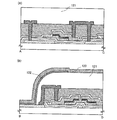
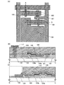
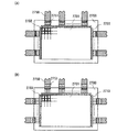
図28(A)は本発明に係る表示パネルの構成を示す上面図であり、絶縁表面を有する基板2700上に画素2702をマトリクス上に配列させた画素部2701、走査線側入力端子2703、信号線側入力端子2704が形成されている。画素数は種々の規格に従って設ければ良く、XGAであれば1024×768×3(RGB)、UXGAであれば1600×1200×3(RGB)、フルスペックハイビジョンに対応させるのであれば1920×1080×3(RGB)とすれば良い。
FIG. 28A is a top view illustrating a structure of a display panel according to the present invention. A
画素2702は、走査線側入力端子2703から延在する走査線と、信号線側入力端子2704から延在する信号線とが交差することで、マトリクス状に配設される。画素2702のそれぞれには、スイッチング素子とそれに接続する画素電極が備えられている。スイッチング素子の代表的な一例はTFTであり、TFTのゲート電極側が走査線と、ソース若しくはドレイン側が信号線と接続されることにより、個々の画素を外部から入力する信号によって独立して制御可能としている。
The
図28(A)は、走査線及び信号線へ入力する信号を、外付けの駆動回路により制御する表示パネルの構成を示しているが、図29(A)に示すように、COG(Chip on Glass)方式によりドライバIC2751を基板2700上に実装しても良い。また他の実装形態として、図29(B)に示すようなTAB(Tape Automated Bonding)方式を用いてもよい。ドライバICは単結晶半導体基板に形成されたものでも良いし、ガラス基板上にTFTで回路を形成したものであっても良い。図29において、ドライバIC2751は、FPC2750と接続している。
FIG. 28A shows a structure of a display panel in which signals input to the scanning lines and signal lines are controlled by an external driver circuit. As shown in FIG. 29A, a COG (Chip on The
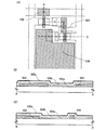
また、画素に設けるTFTをSASで形成する場合には、図28(B)に示すように走査線側駆動回路3702を基板3700上に形成し一体化することもできる。図29(B)において、3701は画素部であり、信号線側駆動回路は、図28(A)と同様に外付けの駆動回路により制御する。画素に設けるTFTを移動度の高い、多結晶(微結晶)半導体、単結晶半導体などで形成する場合は、図28(C)は、走査線駆動回路4702と、信号線駆動回路4704をガラス基板4700上に一体形成することもできる。
In the case where a TFT provided for a pixel is formed using SAS, a scan
本発明は、配線層若しくは電極を形成する導電層や、所定のパターンに形成するためのマスク層など表示パネルを作製するために必要な物体(その目的や機能に応じて膜や層などあらゆる形態で存在する)のうち、少なくとも一つ若しくはそれ以上を、選択的に所望な形状にを形成可能な方法により形成して、表示装置を作製することを特徴とするものである。本発明は、薄膜トランジスタや表示装置を構成する、ゲート電極層、ソース電極層、ドレイン電極層などの導電層、半導体層、マスク層、絶縁膜など、所定の形状を有して形成される全ての構成要素に対して適用できる。 The present invention relates to an object necessary for manufacturing a display panel such as a conductive layer for forming a wiring layer or an electrode or a mask layer for forming a predetermined pattern (all forms such as a film and a layer depending on its purpose and function). The display device is manufactured by forming at least one or more of them in a method that can be selectively formed into a desired shape. The present invention includes all conductive layers such as a gate electrode layer, a source electrode layer, and a drain electrode layer, a semiconductor layer, a mask layer, an insulating film, and the like that constitute a thin film transistor and a display device. Applicable to components.
本実施の形態は、レジストを基板全面に塗布形成しプリベークを行なった後、マスクパターンを介して紫外線等を照射し、現像によってレジストパターンを形成するというフォトリソ工程によりマスクを形成する方法を用いている。該レジストパターンをマスクパターンとしてパターンを形成するべき部分に存在する膜をエッチング除去することにより、所望のパターンを形成する。 This embodiment uses a method of forming a mask by a photolithographic process in which a resist is applied and formed on the entire surface of a substrate and pre-baked, and then ultraviolet rays are irradiated through the mask pattern and a resist pattern is formed by development. Yes. Using the resist pattern as a mask pattern, a film existing in a portion where a pattern is to be formed is removed by etching, thereby forming a desired pattern.
本発明では、形成物のパターニング工程において感光性のレジストや感光性物質を含む材料に光を照射し、露光する工程を行う。露光に用いる光は、特に限定されず、赤外光、可視光、または紫外光のいずれか一またはそれらの組み合わせを用いることが可能である。例えば、紫外線ランプ、ブラックライト、ハロゲンランプ、メタルハライドランプ、キセノンアークランプ、カーボンアークランプ、高圧ナトリウムランプ、または高圧水銀ランプから射出された光を用いてもよい。その場合、ランプ光源は、必要な時間点灯させて照射してもよいし、複数回照射してもよい。 In the present invention, in the patterning step of the formed product, a step of exposing the photosensitive resist or the material containing the photosensitive substance to light is performed. The light used for exposure is not particularly limited, and any one of infrared light, visible light, ultraviolet light, or a combination thereof can be used. For example, light emitted from an ultraviolet lamp, black light, halogen lamp, metal halide lamp, xenon arc lamp, carbon arc lamp, high pressure sodium lamp, or high pressure mercury lamp may be used. In that case, the lamp light source may be lit and irradiated for a necessary time, or may be irradiated multiple times.
露光に用いる光源にレーザ発振器を用いてもよい。レーザ発振器としては、紫外光、可視光、又は赤外光を発振することが可能なレーザ発振器を用いることができる。レーザー発振器としては、KrF、ArF、KrF、XeCl、Xe等のエキシマレーザ発振器、He、He−Cd、Ar、He−Ne、HF等の気体レーザ発振器、YAG、GdVO4、YVO4、YLF、YAlO3などの結晶にCr、Nd、Er、Ho、Ce、Co、Ti又はTmをドープした結晶を使った固体レーザー発振器、GaN、GaAs、GaAlAs、InGaAsP等の半導体レーザ発振器を用いることができる。なお、固体レーザ発振器においては、基本波の第1高調波〜第5高調波を適用するのが好ましい。 A laser oscillator may be used as a light source used for exposure. As the laser oscillator, a laser oscillator that can oscillate ultraviolet light, visible light, or infrared light can be used. As the laser oscillator, excimer laser oscillators such as KrF, ArF, KrF, XeCl, and Xe, gas laser oscillators such as He, He—Cd, Ar, He—Ne, and HF, YAG, GdVO 4 , YVO 4 , YLF, and YAlO Cr crystal such as 3, Nd, Er, Ho, Ce, Co, solid-state laser oscillator using a crystal doped with Ti or Tm, can be used GaN, GaAs, GaAlAs, a semiconductor laser oscillator of InGaAsP or the like. In the solid-state laser oscillator, it is preferable to apply the first to fifth harmonics of the fundamental wave.
感光性物質には大きくわけてネガ型とポジ型がある。ネガ型の場合は、露光された部分で化学反応が生じ、現像液によって化学反応が生じた部分のみが残されてパターンが形成される。また、ポジ型の場合は、露光された部分で化学反応が生じ、現像液によって化学反応が生じた部分が溶解され、露光されなかった部分のみが残されてパターンが形成される。必要に応じてネガ型とポジ型を使い分けるとよい。 Photosensitive materials are roughly divided into negative types and positive types. In the case of the negative type, a chemical reaction occurs in the exposed part, and only the part in which the chemical reaction is caused by the developer is left to form a pattern. In the case of the positive type, a chemical reaction occurs in the exposed portion, the portion in which the chemical reaction has occurred is dissolved by the developing solution, and only the unexposed portion is left to form a pattern. It is good to use a negative type and a positive type as needed.
本実施の形態では、露光は基板表面から行っているが、必要に応じて基板裏面から露光を行ってもよい。 In this embodiment, the exposure is performed from the front surface of the substrate, but the exposure may be performed from the back surface of the substrate as necessary.
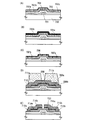
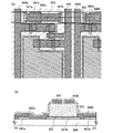
本発明の実施の形態について、図1乃至図6、図8を用いて説明する。より詳しくは、本発明を適用した表示装置の作製方法について説明する。まず、本発明を適用した、チャネルエッチ型の薄膜トランジスタを有する表示装置の作製方法について説明する。図2〜図6(A)は表示装置画素部の上面図であり、図2〜図6の(B)は、図2〜図6(A)における線A―Cによる断面図、図2〜図6の(C)は、図2〜図6(A)における線B−Dによる断面図である。 An embodiment of the present invention will be described with reference to FIGS. 1 to 6 and FIG. More specifically, a method for manufacturing a display device to which the present invention is applied will be described. First, a method for manufacturing a display device having a channel-etched thin film transistor to which the present invention is applied will be described. 2 to 6A are top views of the pixel portion of the display device, and FIG. 2B to FIG. 6B are cross-sectional views taken along line A—C in FIG. 2 to FIG. FIG. 6C is a cross-sectional view taken along line B-D in FIGS.
基板100は、バリウムホウケイ酸ガラス、アルミノホウケイ酸ガラス等からなるガラス基板、石英基板、シリコン基板、金属基板、ステンレス基板又は本作製工程の処理温度に耐えうる耐熱性を有するプラスチック基板を用いる。また、基板100の表面が平坦化されるようにCMP法などによって、研磨しても良い。なお、基板100上に、絶縁層を形成してもよい。絶縁層は、CVD法、プラズマCVD法、スパッタリング法、スピンコート法等の公知の方法により、珪素を含む酸化物材料、窒化物材料を用いて、単層又は積層して形成される。この絶縁層は、形成しなくても良いが、基板100からの汚染物質などを遮断する効果がある。基板100として、320mm×400mm、370mm×470mm、550mm×650mm、600mm×720mm、680mm×880mm、1000mm×1200mm、1100mm×1250mm、1150mm×1300mmのような大面積基板を用いることができる。
As the
基板100上に導電膜101を形成する。導電膜101は、パターニングされゲート電極層と画素電極層となる。導電膜101は、印刷法、電界メッキ法、PVD法(Physical Vapor Deposition)、CVD法(Chemical Vapor Deposition)、蒸着法等の公知の手法により高融点材料を用いて形成することが好ましい。高融点材料を用いることにより、後の加熱工程が可能となる。高融点材料としては、タングステン(W)、モリブデン(Mo)、ジルコニウム(Zr)、ハフニウム(Hf)、バナジウム(V)、ニオブ(Nb)、タンタル(Ta)、クロム(Cr)、コバルト(Co)、ニッケル(Ni)、白金(Pt)等の金属又はその合金、若しくはその金属窒化物を適宜用いることができる。また、これら複数の層を積層して形成しても良い。代表的には、基板表面に窒化タンタル膜、その上にタングステン膜を積層してもよい。このような反射性を有する金属は、反射型の表示パネルを作製する場合には好ましい。また、珪素に一導電型を付与する不純物元素を添加した材料を用いても良い。例えば、非晶質珪素膜にリン(P)などのn型を付与する不純物元素が含まれたn型を有する珪素膜などを用いることができる。
A
導電膜101は、画素電極層としても機能するので、透明導電性材料を用いて形成することもできる。画素電極層は、透過型の表示パネルを作製する場合には、インジウム錫酸化物(ITO)、酸化珪素を含むインジウム錫酸化物(ITSO)、酸化亜鉛(ZnO)、酸化スズ(SnO2)などにより形成してもよい。好ましくは、スパッタリング法によりインジウム錫酸化物(ITO)、酸化珪素を含むインジウム錫酸化物(ITSO)、酸化亜鉛(ZnO)などで形成する。より好ましくは、ITOに酸化珪素が2〜10重量%含まれたターゲットを用いてスパッタリング法で酸化珪素を含む酸化インジウムスズを用いる。この他、酸化珪素を含み酸化インジウムに2〜20%の酸化亜鉛(ZnO)を混合した酸化インジウム酸化亜鉛合金などの導電性材料を用いても良い。
Since the
本実施の形態では、導電膜101は、導電性材料としてインジウム錫酸化物(ITO)をスパッタリング法により形成し、550℃で焼成して導電膜101を形成する。また、電極層となる導電膜101は、複数の導電性材料を積層しても良い。
In this embodiment, the
導電膜101上にフォトリソ工程を用いてレジストからなるマスク102a、マスク102bを形成する。(図2参照。)。
A
マスクは、感光剤を含む市販のレジスト材料を用いてもよく、例えば、代表的なポジ型レジストである、ノボラック樹脂と感光剤であるナフトキノンジアジド化合物、ネガ型レジストであるベース樹脂、ジフェニルシランジオール及び酸発生剤などを用いてもよい。いずれの材料を用いるとしても、その表面張力と粘度は、溶媒の濃度を調整したり、界面活性剤等を加えたりして適宜調整する。また導電膜101に感光性を有する感光性物質を含む導電性材料を用いると、レジストからなるマスクを形成しなくても導電膜101に直接レーザ光を照射し、露光、エッチャントによる除去を行うことで、所望のパターンにパターニングすることができる。この場合、マスクを形成せずともよいので工程が簡略化する利点がある。感光性物質を含む導電性材料は、Ag、Au、Cu、Ni、Al、Ptなどの金属或いは合金と、有機高分子樹脂、光重合開始剤、光重合単量体、または溶剤などからなる感光性樹脂とを含んだものを用いればよい。有機高分子樹脂としては、ノボラック樹脂、アクリル系コポリマー、メタクリル系コポリマー、セルローズ誘導体、環化ゴム系樹脂などを用いる。
For the mask, a commercially available resist material containing a photosensitizer may be used. For example, a novolak resin that is a typical positive resist and a naphthoquinonediazide compound that is a photosensitizer, a base resin that is a negative resist, diphenylsilanediol In addition, an acid generator or the like may be used. Whichever material is used, the surface tension and viscosity are appropriately adjusted by adjusting the concentration of the solvent or adding a surfactant or the like. Further, when a conductive material containing a photosensitive material having photosensitivity is used for the
このように微細に加工されたマスク102a、マスク102bを用いて導電膜101をパターニングし、ゲート電極層103、ゲート電極層104、及び画素電極層となる第1の電極層120を形成する(図3参照。)。
The
次に、ゲート電極層103、ゲート電極層104、画素電極層120の上にゲート絶縁膜105a、ゲート絶縁膜105b、ゲート絶縁膜105cを形成し3層の積層構造とする。半導体層に接するゲート絶縁膜105cの膜厚は、0.1nm以上10nm以下(好ましくは1nm以上3nm以下)とすることが望ましい。このような構造であると、半導体層中の金属元素のゲッタリング効率も上がり、かつ半導体層への窒化珪素膜の悪影響も軽減できる。また積層される絶縁膜は、同チャンバー内で真空を破らずに同一温度下で、反応ガスを切り変えながら連続的に形成するとよい。真空を破らずに連続的に形成すると、積層する膜同士の界面が汚染されるのを防ぐことができる。
Next, a
ゲート絶縁膜105a、ゲート絶縁膜105b、ゲート絶縁膜105cは、酸化珪素(SiOx)、窒化珪素(SiNx)、酸化窒化珪素(SiOxNy)(x>y)、窒化酸化珪素(SiNxOy)(x>y)などを適宜用いることができる。更には、ゲート電極層103を陽極酸化して、ゲート絶縁膜105aの代わりに、陽極酸化膜を形成しても良い。なお、基板側から不純物などの拡散を防止するため、ゲート絶縁膜105aとしては、窒化珪素(SiNx)、窒化酸化珪素(SiNxOy)(x>y)などを用いて形成することが好ましい。また、ゲート絶縁膜105bとしては、酸化珪素(SiOx)、酸化窒化珪素(SiOxNy)(x>y)を用いて形成することが望ましい。なお、ゲート絶縁膜105bには、水素が含まれている。また、ゲート絶縁膜105cとしては窒化珪素膜(SiNx)、あるいは窒化酸化珪素膜(SiNxOy)(x>y)などを用いて形成することが好ましい。なお、低い成膜温度でゲートリーク電流に少ない緻密な絶縁膜を形成するには、アルゴンなどの希ガス元素を反応ガスに含ませ、形成される絶縁膜中に混入させると良い。本実施の形態では、SiH4、NH3を反応ガスとして窒化珪素膜を膜厚50nm〜140nmでゲート絶縁膜105aを形成し、SiH4及びN2Oを反応ガスとして酸化珪素膜を膜厚100nmでゲート絶縁膜105bを積層した後、SiH4、NH3を反応ガスとして窒化珪素膜を膜厚1nm〜3nmでゲート絶縁膜105cを形成する。なお、ゲート絶縁膜105a及びゲート絶縁膜105bの膜厚をそれぞれ50nm〜100nmとすると好ましい。また、ゲート絶縁膜105cはその形成条件によっては膜厚は極薄であり、膜として形態を保っていなくてもよい。
The
次に半導体膜を形成する。半導体層の詳細な作製方法を図8を用いて説明する。半導体膜は25〜200nm(好ましくは30〜150nm)の厚さで公知の手段(スパッタ法、LPCVD法、またはプラズマCVD法等)により成膜すればよい。本実施の形態では、非晶質半導体膜を結晶化し、結晶性半導体膜とするものを用いるのが好ましい。 Next, a semiconductor film is formed. A detailed method for manufacturing the semiconductor layer will be described with reference to FIGS. The semiconductor film may be formed by a known means (a sputtering method, an LPCVD method, a plasma CVD method, or the like) with a thickness of 25 to 200 nm (preferably 30 to 150 nm). In this embodiment mode, it is preferable to use a crystallized semiconductor film obtained by crystallizing an amorphous semiconductor film.
半導体膜を形成する材料は、シランやゲルマンに代表される半導体材料ガスを用いて気相成長法やスパッタリング法で作製される非晶質半導体(以下「アモルファス半導体:AS」ともいう。)、該非晶質半導体を熱エネルギーを利用して結晶化させた多結晶半導体、或いはセミアモルファス(微結晶若しくはマイクロクリスタルとも呼ばれる。以下「SAS」ともいう。)半導体などを用いることができる。 As a material for forming the semiconductor film, an amorphous semiconductor (hereinafter also referred to as “amorphous semiconductor: AS”) manufactured by a vapor deposition method or a sputtering method using a semiconductor material gas typified by silane or germane is used. A polycrystalline semiconductor obtained by crystallizing a crystalline semiconductor using thermal energy, a semi-amorphous (also referred to as microcrystal or microcrystal, hereinafter, also referred to as “SAS”) semiconductor, or the like can be used.
SASは、非晶質と結晶構造(単結晶、多結晶を含む)の中間的な構造を有し、自由エネルギー的に安定な第3の状態を有する半導体であって、短距離秩序を持ち格子歪みを有する結晶質な領域を含んでいる。少なくとも膜中の一部の領域には、0.5〜20nmの結晶領域を観測することが出来、珪素を主成分とする場合にはラマンスペクトルが520cm-1よりも低波数側にシフトしている。X線回折では珪素結晶格子に由来するとされる(111)、(220)の回折ピークが観測される。未結合手(ダングリングボンド)の中和剤として水素またはハロゲンを少なくとも1原子%またはそれ以上含ませている。SASは、珪化物気体をグロー放電分解(プラズマCVD)して形成する。珪化物気体としては、SiH4、その他にもSi2H6、SiH2Cl2、SiHCl3、SiCl4、SiF4などを用いることが可能である。またF2、GeF4を混合させても良い。この珪化物気体をH2、又は、H2とHe、Ar、Kr、Neから選ばれた一種または複数種の希ガス元素で希釈しても良い。希釈率は2〜1000倍の範囲、圧力は概略0.1Pa〜133Paの範囲、電源周波数は1MHz〜120MHz、好ましくは13MHz〜60MHzである。基板加熱温度は300℃以下が好ましく、100〜200℃の基板加熱温度でも形成可能である。ここで、主に成膜時に取り込まれる不純物元素として、酸素、窒素、炭素などの大気成分に由来する不純物は1×1020cm-3以下とすることが望ましく、特に、酸素濃度は5×1019cm-3以下、好ましくは1×1019cm-3以下となるようにすることが好ましい。また、ヘリウム、アルゴン、クリプトン、ネオンなどの希ガス元素を含ませて格子歪みをさらに助長させることで安定性が増し良好なSASが得られる。また半導体膜としてフッ素系ガスより形成されるSAS層に水素系ガスより形成されるSAS層を積層してもよい。 SAS is a semiconductor having an intermediate structure between amorphous and crystalline structures (including single crystal and polycrystal) and having a third state that is stable in terms of free energy and has a short-range order and a lattice. It includes a crystalline region with strain. A crystal region of 0.5 to 20 nm can be observed in at least a part of the film, and when silicon is the main component, the Raman spectrum shifts to a lower wave number side than 520 cm −1. Yes. In X-ray diffraction, diffraction peaks of (111) and (220) that are derived from the silicon crystal lattice are observed. At least 1 atomic% or more of hydrogen or halogen is contained as a neutralizing agent for dangling bonds. The SAS is formed by glow discharge decomposition (plasma CVD) of a silicide gas. As the silicide gas, SiH 4 , Si 2 H 6 , SiH 2 Cl 2 , SiHCl 3 , SiCl 4 , SiF 4, and the like can be used. Further, F 2 and GeF 4 may be mixed. This silicide gas may be diluted with H 2 , or H 2 and one or more kinds of rare gas elements selected from He, Ar, Kr, and Ne. The dilution rate is in the range of 2 to 1000 times, the pressure is in the range of approximately 0.1 Pa to 133 Pa, and the power supply frequency is 1 MHz to 120 MHz, preferably 13 MHz to 60 MHz. The substrate heating temperature is preferably 300 ° C. or lower, and can be formed even at a substrate heating temperature of 100 to 200 ° C. Here, as an impurity element mainly taken in at the time of film formation, it is desirable that impurities derived from atmospheric components such as oxygen, nitrogen, and carbon be 1 × 10 20 cm −3 or less. It is preferable to be 19 cm −3 or less, preferably 1 × 10 19 cm −3 or less. Further, by adding a rare gas element such as helium, argon, krypton, or neon to further promote lattice distortion, stability is improved and a favorable SAS can be obtained. In addition, a SAS layer formed of a hydrogen-based gas may be stacked on a SAS layer formed of a fluorine-based gas as a semiconductor film.
なお、後の結晶化で良質な結晶構造を有する半導体膜を得るためには、図8に示す非晶質半導体膜404膜中に含まれる酸素、窒素などの不純物濃度を5×10¹⁸/cm3(以下、濃度はすべて二次イオン質量分析法(SIMS)にて測定した原子濃度として示す。)以下に低減させておくと良い。これらの不純物は、触媒元素と反応しやすく、後の結晶化を妨害する要因となり、また、結晶化後においても捕獲中心や再結合中心の密度を増加させる要因となる。
In order to obtain a semiconductor film having a good crystal structure by subsequent crystallization, the concentration of impurities such as oxygen and nitrogen contained in the
本実施の形態では、非晶質半導体膜、又はSAS膜に結晶化を助長する元素を用いた熱結晶化法を用いる。加熱方法としてGRTA(Gas Rapid Thermal Anneal)法、LRTA(Lamp Rapid Thermal Anneal)法等のRTA法がある。 In this embodiment mode, a thermal crystallization method using an element that promotes crystallization is used for an amorphous semiconductor film or a SAS film. As a heating method, there are RTA methods such as a GRTA (Gas Rapid Thermal Anneal) method and an LRTA (Lamp Rapid Thermal Anneal) method.
非晶質半導体膜への金属元素の導入の仕方としては、当該金属元素を非晶質半導体膜の表面又はその内部に存在させ得る手法であれば特に限定はなく、例えばスパッタ法、CVD法、プラズマ処理法(プラズマCVD法も含む)、吸着法、金属塩の溶液を塗布する方法、イオン注入法、イオンドーピング法を使用することができる。このうち溶液を用いる方法は簡便であり、金属元素の濃度調整が容易であるという点で有用である。また、このとき金属元素膜を形成する下地膜の表面のぬれ性を改善し、下地膜の表面全体に水溶液を行き渡らせるため、酸素雰囲気中でのUV光の照射、熱酸化法、ヒドロキシラジカルを含むオゾン水又は過酸化水素による処理等により、酸化膜を成膜することが望ましい。 The method of introducing the metal element into the amorphous semiconductor film is not particularly limited as long as the metal element can be present on the surface of the amorphous semiconductor film or inside the amorphous semiconductor film. For example, sputtering, CVD, Plasma treatment methods (including plasma CVD methods), adsorption methods, metal salt solution coating methods, ion implantation methods, and ion doping methods can be used. Among these, the method using a solution is simple and useful in that the concentration of the metal element can be easily adjusted. At this time, in order to improve the wettability of the surface of the base film on which the metal element film is formed and to spread the aqueous solution over the entire surface of the base film, irradiation with UV light in an oxygen atmosphere, thermal oxidation method, hydroxy radical It is desirable to form an oxide film by treatment with ozone water or hydrogen peroxide.
本実施の形態では、ゲート絶縁膜105c上に、結晶化を助長する元素としてNiを用い、Ni元素を重量換算で10ppmを含有した水溶液をスピンコーティング法により塗布し、金属膜403を形成する(図8(A)参照。)。結晶化を助長する元素としては、この珪素の結晶化を助長する金属元素としては鉄(Fe)、ニッケル(Ni)、チタン(Ti)コバルト(Co)、ルテニウム(Ru)、ロジウム(Rh)、パラジウム(Pd)、オスニウム(Os)、イリジウム(Ir)、白金(Pt)、銅(Cu)及び金(Au)から選ばれた一種又は複数種類を用いて、金属膜403を形成することができる。金属膜403はその形成条件によっては膜厚が極薄であり、膜として形態を保っていなくてもよい。結晶化を助長させる効果が得られるように、後の工程で形成する非晶質半導体膜404に接して形成されればよい。
In this embodiment mode, a
金属膜403上に非晶質半導体膜404を形成する。非晶質半導体膜404としては、SiH4、H2の反応ガスにより形成する非晶質珪素を用いる。本実施の形態では、非晶質半導体膜404中の酸素濃度を5×10¹⁹atom/cm3以下、好ましくは2×1019atom/cm3以下で形成することにより、金属元素として添加したNiがゲッタリングしやすくなる。非晶質半導体膜404の膜厚は30nm〜150nmが好ましい。本実施の形態では、非晶質半導体膜404を150nm形成する。
An
金属元素を用いた結晶化を行った場合、金属元素を低減、又は除去するためにゲッタリング工程を施す。金属膜403の金属元素が非晶質半導体膜404中に拡散し結晶化に寄与した後、金属元素を吸い込み自らに取り込む層として半導体膜を、非晶質半導体膜404に接して形成する。本実施の形態では、不純物を有する非晶質半導体膜をゲッタリングシンクとして金属元素を捕獲する。
When crystallization using a metal element is performed, a gettering step is performed in order to reduce or remove the metal element. After the metal element of the
非晶質半導体膜404上にプラズマCVD法を用いて、半導体膜405a、半導体膜405bを形成する。半導体膜405a、半導体膜405bは不純物元素を有しており、不純物元素としてはn型を付与する不純物元素や希ガス元素などを用いることができ、例えばリン(P)、窒素(N)、ヒ素(As)、アンチモン(Sb)、ビスマス(Bi)、ヘリウム(He)、ネオン(Ne)、アルゴン(Ar)、Kr(クリプトン)、Xe(キセノン)から選ばれた一種または複数種を用いることができる。n型を付与する不純物元素を含むn型を有する半導体膜に、アルゴンなどの希ガス元素が含まれるように形成することもできる。本実施の形態では、半導体膜405aを半導体膜405bには、n型を付与する不純物元素(本実施の形態ではリンを用いる)が含まれており、半導体膜405aの不純物元素の濃度は、半導体膜405bより低くなるように形成されている。前記不純物元素は、CVD法などによって、不純物元素を含むように半導体膜を形成しても良いし、半導体膜を形成後に、イオンドーピング法などによって添加してもよい。また、本実施の形態において、非晶質半導体膜404、半導体膜405a、半導体膜405bは、同チャンバー内で真空を破らずに同一温度(本実施の形態では330℃)下で、反応ガスを切り変えながら連続的に形成する。非晶質半導体膜404を成膜後、半導体膜405a、半導体膜405bを形成する。
A
このときのn型を付与する不純物元素が含まれる半導体膜の不純物のプロファイルを図37に示す。図37(A)は、結晶性半導体膜903上に、プラズマCVD法によりn型を付与する不純物元素が含まれる半導体膜901a、901bを形成した時のn型を付与する不純物元素のプロファイル900aを示す。半導体膜901a、半導体膜901bは、半導体膜405a、半導体膜405bと対応しており、半導体膜901aはn型の低濃度不純物領域(n−領域ともいう)として形成され、半導体膜901bはn型の高濃度不純物領域(n+領域ともいう)として形成されている。よって半導体膜901a、半導体膜901bのそれぞれの膜において深さ方向に対して一定の濃度のn型を付与する不純物元素が分布しており、半導体膜901aの方が、半導体膜901bより低い濃度でn型を付与する不純物元素が分布している。n+領域である半導体膜901bは後にソース領域及びドレイン領域として機能し、n−領域である半導体膜901aはLDD(LightlyDoped Drain)領域として機能する。なお、n+領域とn−領域はそれぞれ作り分けているので界面が存在する。n+領域とn−領域の膜厚制御は、それぞれ各濃度の半導体膜の膜厚を制御することによって達成できる。
FIG. 37 shows the impurity profile of the semiconductor film containing the impurity element imparting n-type conductivity at this time. FIG. 37A shows a
図37(A)で形成した半導体膜901a及び半導体膜901bにp型を付与する不純物元素としてボロンをイオンドープ法又はイオン注入法によって添加して半導体膜911を形成した時のp型を付与する不純物元素のプロファイル913を図38(A)に示す。p型を付与する不純物元素の濃度の方が、n型を付与する不純物元素の濃度より高く、半導体膜911はp型のを有する半導体膜となっているのがわかる。また、p型を付与する不純物元素は、チャネルドープされるため、結晶性半導体膜903にも添加されている。図38(A)に示すように、半導体膜911の表面付近は、p型を付与する不純物元素濃度が比較的が高いp型の不純物領域(p+領域ともいう)912bとなっており、一方、結晶性半導体膜903に近づくにつれ、p型を付与する不純物元素濃度が比較的減少しておりp型の低濃度不純物領域(p−領域ともいう)912aとなっている。
As the impurity element imparting p-type conductivity to the
一方、図37(B)は、結晶性半導体膜903上に、非晶質半導体、SAS、微結晶半導体、及び結晶性半導体から選ばれたいずれかの状態を有する膜の半導体膜を形成し、イオンドープ法又はイオン注入法により該半導体膜にn型を付与する不純物元素を添加して半導体膜902を形成した時のn型を付与する不純物元素のプロファイル900bを示す。図37(B)に示すように、半導体膜902の表面付近は、n型を付与する不純物元素濃度が比較的が高い。n型を付与する不純物元素濃度が1×10¹⁹/cm3以上の領域をn型の高濃度不純物領域(n+領域ともいう)904bと示す。一方、結晶性半導体膜903に近づくにつれ、n型を付与する不純物元素濃度が比較的減少している。n型を付与する不純物元素濃度が5×1017〜1×1019/cm3の領域をn型の低濃度不純物領域(n−領域ともいう)904aと示す。n+領域904bは後にソース領域及びドレイン領域として機能し、n−領域904aはLDD領域として機能する。なお、n+領域とn−領域それぞれの界面は存在せず、相対的なn型を付与する不純物元素濃度の濃度の大小によって変化する。このようにイオンドープ法又はイオン注入法により形成されたn型を付与する不純物元素が含まれる半導体膜902は、添加条件によって濃度プロファイルを制御することが可能であり、n+領域とn−領域の膜厚を適宜制御することが可能である。n+領域とn−領域を有することにより電界の緩和効果が大きくなり、ホットキャリア耐性を高めた薄膜トランジスタを形成することが可能となる。
On the other hand, in FIG. 37B, a semiconductor film having a state selected from an amorphous semiconductor, a SAS, a microcrystalline semiconductor, and a crystalline semiconductor is formed over the
図37(B)で形成した半導体膜902にp型を付与する不純物元素としてボロンをイオンドープ法又はイオン注入法によって添加して半導体膜921を形成した時のp型を付与する不純物元素のプロファイル923を図38(B)に示す。p型を付与する不純物元素の濃度の方が、n型を付与する不純物元素の濃度より高く、半導体膜921はp型を有する半導体膜(p型の不純物領域を有する半導体膜ともいえる)となっているのがわかる。また、p型を付与する不純物元素は、チャネルドープされるため、結晶性半導体膜903にも添加されている。図38(B)に示すように、半導体膜921の表面付近は、p型を付与する不純物元素濃度が比較的が高いp型の不純物領域(p+領域ともいう)922bとなっており、一方、結晶性半導体膜903に近づくにつれ、p型を付与する不純物元素濃度が比較的減少しておりp型の低濃度不純物領域(p−領域ともいう)922aとなっている。また、n型を付与する不純物元素の添加工程で、その添加条件によって、膜表面の不純物元素濃度が高くなっている場合がある。このような場合は、膜表面を薄くエッチングし、高不純物元素濃度領域の膜を除去してから、p型を付与する不純物元素を添加する工程を行えばよい。
Profile of the impurity element imparting p-type when boron is added to the
本実施の形態では、半導体膜405a、半導体膜405bとして、n型を付与する不純物元素(ドナー型元素)であるリンを含むn型を有する半導体膜をプラズマCVD法によって形成する。また、半導体膜405a、半導体膜405bに含まれるn型を付与する不純物元素の濃度を異ならせているので、半導体膜405aはn型の低濃度不純物領域となり、半導体膜405bはn型の高濃度不純物領域となっている。n型の低濃度不純物領域の不純物濃度は、1×10¹⁷〜3×10¹⁹/cm3、好ましくは1×1018〜1×1019/cm3、n型の高濃度不純物領域の不純物濃度は、その10倍から100倍が好ましく、1×1019〜3×1021/cm3とすることができる。またn型の低濃度不純物領域である半導体膜405aの膜厚は20〜200nm、代表的には50〜150nmであり、本実施の形態では、膜厚50nmで形成する。n型の高濃度不純物領域である半導体膜405bの膜厚は30〜100nm、代表的には40〜60nmであり、本実施の形態では、膜厚50nmで形成する。
In this embodiment, as the
その後、熱処理を行い、非晶質半導体膜を結晶化して結晶性半導体膜406の形成と、結晶性半導体膜406中の金属元素を低減、又は除去するためにゲッタリング工程を同時に行なう。この場合、結晶化は半導体の結晶化を助長する金属元素が接した半導体膜の部分でシリサイドが形成され、それを核として結晶化が進行する。ここでは、脱水素化のための熱処理の後、結晶化とゲッタリング工程のための熱処理(550℃〜650℃で5分〜24時間)を行う。また、RTA、GRTAにより結晶化とゲッタリング工程を行っても良い。ここで、加熱にレーザ光照射を行わず結晶化することで、結晶性のばらつきを低減することが可能であり、後に形成されるTFTのばらつきを抑制することが可能である。又、本実施の形態では、不純物を有する非晶質半導体膜をゲッタリングシンクとして結晶性半導体膜406に接して形成しているため、金属元素は、図8(C)に示すように、矢印の方向へ加熱処理によって移動し、半導体膜405a、半導体膜405b中に捕獲される。半導体膜405a、半導体膜405bは金属元素を含む半導体膜408a、半導体膜408bとなる。本実施の形態では半導体膜408a、半導体膜408bにはn型を付与する不純物元素と、結晶化を助長する金属元素が含まれる。この工程により、結晶性半導体膜406中の結晶化を促進させる元素(本実施の形態ではニッケル元素)がデバイス特性に影響を与えない濃度、即ち膜中のニッケル濃度が1×1018/cm3以下、望ましくは1×1017/cm3以下とすることができる。また、ゲッタリング後の金属触媒が移動した半導体膜408a、半導体膜408bも加熱処理により結晶化される場合がある。なお、本実施の形態においては、ゲッタリング工程と共に、半導体膜408a、半導体膜408b中のn型を付与する不純物元素(ドナー型元素)の活性化を行っている。熱処理は窒素雰囲気下で行ってもよい。また、本実施の形態では、熱処理を550℃で4時間行うが、熱処理をRTA法により650℃で6分間で行ってもよい。
After that, heat treatment is performed, and the amorphous semiconductor film is crystallized to form the
このようにして得られた結晶性半導体膜406に対して、薄膜トランジスタのしきい値電圧を制御するために微量な不純物元素(ボロンまたはリン)のドーピングを行ってもよい。この不純物元素のドーピングは、結晶化工程の前の非晶質半導体膜に行ってもよいし、結晶性半導体膜406中の金属元素をゲッタリング工程によって軽減、除去した後行ってもよい。本実施の形態ではジボラン(B2H6)を質量分離しないでプラズマ励起したイオンドープ法でボロンを添加する。なお、質量分離を行うイオン注入法を用いてもよい。非晶質半導体膜の状態で不純物元素をドーピングすると、その後の結晶化のための加熱処理によって、不純物の活性化も行うことができる。また、ドーピングの際に生じる欠陥等も改善することができる。
The
次に結晶性半導体膜406、半導体膜408a、半導体膜408b上にフォトリソ工程を用いてレジストからなるマスクを形成し、微細に加工されたマスクを用いて結晶性半導体膜406、半導体膜408a、半導体膜408bをパターニングし、結晶性半導体層106、半導体層108、半導体層110、を形成する(図4参照。)。同様に、結晶性半導体層107、半導体層109、半導体層111を形成する。フォトマスクはマスク102aを形成したときと同様にフォトリソ工程よって微細なパターンのマスクを形成すればよい。微細なパターンのマスクによって半導体膜は微細かつ精巧に所望な形状にパターニングすることができる。
Next, a resist mask is formed over the
パターニングの際のエッチング加工は、プラズマエッチング(ドライエッチング)又はウエットエッチングのどちらを採用しても良いが、大面積基板を処理するにはプラズマエッチングが適している。エッチングガスとしては、CF4、NF3、SF6、CHF3などのフッ素系又はCl2、BCl3、SiCl4もしくはCCl4などを代表とする塩素系ガス、あるいはO2のガスを用い、HeやArなどの不活性ガスを適宜加えても良い。また、大気圧放電のエッチング加工を適用すれば、局所的な放電加工も可能であり、基板の全面にマスク層を形成する必要はない。 As the etching process at the time of patterning, either plasma etching (dry etching) or wet etching may be employed, but plasma etching is suitable for processing a large area substrate. As an etching gas, a fluorine-based gas such as CF 4 , NF 3 , SF 6 , or CHF 3 , a chlorine-based gas typified by Cl 2 , BCl 3 , SiCl 4, CCl 4, or the like, or an O 2 gas is used. An inert gas such as Ar or Ar may be added as appropriate. Further, if an atmospheric pressure discharge etching process is applied, a local electric discharge process is also possible, and it is not necessary to form a mask layer on the entire surface of the substrate.
なお、以下の実施形態及び実施例のフォトリソグラフィ工程において、レジストを塗布する前に、半導体膜表面に、膜厚が数nm程度の絶縁膜を形成することが好ましい。この工程により半導体膜とレジストとが直接接触すること回避することが可能であり、不純物が半導体膜中に侵入するのを防止できる。なお、絶縁膜の形成方法としては、オゾン水等の酸化力のある溶液を塗布する方法、酸素プラズマ、オゾンプラズマを照射する方法等が挙げられる。 In the photolithography processes of the following embodiments and examples, it is preferable to form an insulating film having a thickness of several nanometers on the surface of the semiconductor film before applying the resist. By this step, it is possible to avoid direct contact between the semiconductor film and the resist, and impurities can be prevented from entering the semiconductor film. Note that examples of a method for forming the insulating film include a method of applying an oxidizing solution such as ozone water, a method of irradiating oxygen plasma, ozone plasma, and the like.
次に導電膜をスパッタリング法により形成し、導電膜上にフォトリソ工程を用いてレジストからなるマスクを形成する。マスクを用いて、ソース電極層又はドレイン電極層112、ソース電極層又はドレイン電極層113、ソース電極層又はドレイン電極層114、ソース電極層又はドレイン電極層115を形成し、該ソース電極層又はドレイン電極層112、ソース電極層又はドレイン電極層113、ソース電極層又はドレイン電極層114、ソース電極層又はドレイン電極層115をマスクとして、半導体層106、n型を有する半導体層108及びn型を有する半導体層110、半導体層107、n型を有する半導体層109及びn型を有する半導体層111をパターン加工して、半導体層146、n型を有する半導体層148b及びn型を有する半導体層150b、半導体層147、n型を有する半導体層149a、n型を有する半導体層149b、n型を有する半導体層151a、n型を有する半導体層151bを形成する(図5参照。)。ソース電極層又はドレイン電極層112、ソース電極層又はドレイン電極層113、ソース電極層又はドレイン電極層114、ソース電極層又はドレイン電極層115を形成する工程も、前述したゲート電極層103とを形成したときと同様に形成することができる。ソース電極層又はドレイン電極層112、ソース電極層又はドレイン電極層114は配線層としても機能する。
Next, a conductive film is formed by a sputtering method, and a resist mask is formed over the conductive film using a photolithography process. A source or drain
ソース電極層又はドレイン電極層を形成する導電性材料としては、Ag(銀)、Au(金)、Cu(銅)、W(タングステン)、Al(アルミニウム)等を主成分とした金属を用いることができる。また、透光性を有するインジウム錫酸化物(ITO)、インジウム錫酸化物と酸化珪素からなるITSO、有機インジウム、有機スズ、酸化亜鉛、窒化チタンなどを組み合わせても良い。 As a conductive material for forming the source electrode layer or the drain electrode layer, a metal whose main component is Ag (silver), Au (gold), Cu (copper), W (tungsten), Al (aluminum), or the like is used. Can do. Further, light-transmitting indium tin oxide (ITO), ITSO made of indium tin oxide and silicon oxide, organic indium, organic tin, zinc oxide, titanium nitride, or the like may be combined.
ソース電極層又はドレイン電極層112、ソース電極層又はドレイン電極層113、ソース電極層又はドレイン電極層114、ソース電極層又はドレイン電極層115は、微細なパターンで形成されており、制御性よく形成しなければ形成不良によるショート等の不良を引き起こす。よって、本実施の形態では、半導体層上の微細なパターニングはフォトマスクを作製し、フォトリソグラフィ法を用いたパターニング処理により行う。図4で示すように、基板上にゲート電極層、ゲート絶縁膜、半導体層、n型を有する半導体層が形成されており、これらを覆うように導電膜を全面に形成する。導電膜は蒸着法、CVD法、スパッタ法などによって形成することができる。その後、レジストからなるマスクを形成する。レジストからなるマスクに、光を照射し、露光することによってを感光を行なう。本実施の形態ではポジ型の感光性のレジストを用いるため、露光された領域はエッチャントによって除去され、開口部が形成される。開口部を有するマスクを用いて導電膜をエッチングによりパターニングすることによって、ソース電極層又はドレイン電極層112、ソース電極層又はドレイン電極層113、ソース電極層又はドレイン電極層114、ソース電極層又はドレイン電極層115が形成される。
The source or drain
ソース電極層又はドレイン電極層、半導体層、ゲート電極層、ゲート絶縁膜を覆うようにパッシベーション膜となる絶縁膜140を成膜することが好ましい。絶縁膜140は、プラズマCVD法又はスパッタリング法などの薄膜形成法を用い、窒化珪素、酸化珪素、窒化酸化珪素、酸化窒化珪素、酸化窒化アルミニウム、または酸化アルミニウム、ダイアモンドライクカーボン(DLC)、窒素含有炭素(CN)、その他の絶縁性材料を用いて形成することができる。なお、パッシベーション膜は単層でも積層構造でもよい。ここでは、半導体層146、半導体層147の界面特性から酸化珪素、又は酸化窒化珪素を形成したのち、外部からの不純物が半導体素子内に侵入するのを防ぐため窒化珪素、又は窒化酸化珪素を形成する積層構造が好ましい。本実施の形態では、半導体層146、半導体層147に接して、酸化珪素膜を膜厚150nm形成した後、同チャンバー内でガス切り替えを行い連続的に窒化珪素膜を膜厚200nm形成する積層構造で絶縁膜140を形成する。
An insulating
この後半導体層146、半導体層147を水素雰囲気又は窒素雰囲気で加熱して水素化することが好ましい。なお、窒素雰囲気で加熱する場合は、絶縁膜140として水素を含む絶縁膜を形成することが好ましい。
Thereafter, the
次に、絶縁膜116を形成する。本実施の形態では、絶縁膜110を全面に形成し、レジスト等のマスクによって、エッチングしパターニングする。
Next, the insulating
絶縁膜110は、酸化珪素、窒化珪素、酸化窒化珪素、酸化アルミニウム、窒化アルミニウム、酸化窒化アルミニウム、ダイアモンドライクカーボン(DLC)、窒素含有炭素膜(CN)その他の無機絶縁性材料、又はアクリル酸、メタクリル酸及びこれらの誘導体、又はポリイミド(polyimide)、芳香族ポリアミド、ポリベンゾイミダゾール(polybenzimidazole)、ベンゾシクロブテン、ポリシラザンなどの有機絶縁性材料、又はシロキサン系材料を出発材料として形成された珪素、酸素、水素からなる化合物のうちSi−O−Si結合を含む無機シロキサン、珪素上の水素がメチルやフェニルのような有機基によって置換された有機シロキサン系の絶縁材料で形成することができる。アクリル、ポリイミド等の感光性、非感光性の材料を用いて形成してもよい。
The insulating
本実施の形態では、絶縁膜116の材料としては、シリコン(Si)と酸素(O)との結合で骨格構造が構成され、置換基に水素、フッ素、アルキル基、または芳香族炭化水素のうち少なくとも1種を有する材料を用いた塗布膜を用いる。焼成した後の膜は、アルキル基を含む酸化珪素膜(SiOx)とも呼べる。
In this embodiment, as a material of the insulating
絶縁膜140及び絶縁膜116にソース電極層又はドレイン電極層113に達する開口部136と、ソース電極層又はドレイン電極層115に達する開口部138、ゲート絶縁膜105a、ゲート絶縁膜105b、ゲート絶縁膜105c、絶縁膜140、絶縁膜116、だ第1の電極層120に達する開口部139、ゲート電極層103に達する開口部135、ゲート電極層104に達する開口部137を形成する。この開口部もレジストからなるマスクを用いてエッチングし形成する。パターニングに用いるマスクは、フォトリソ工程を用いて形成する。このようにして形成した開口部138及び開口部139に配線層119を形成し、ソース電極層又はドレイン電極層115と第1の電極層120とを電気的に接続する。また、開口部136及び開口部137に配線層118を形成し、ソース電極層又はドレイン電極層113とゲート電極層104とを電気的に接続する。また、開口部135にもゲート電極層103と電気的に接続するようにゲート配線層117を形成する。ゲート配線層117を低抵抗な材料によって形成することで、ゲート電極層103が多少高抵抗の材料であっても、高速動作が可能となり、大きな電流も流すことができる。
An
以上の工程により、基板100上にボトムゲート型(逆スタガ型ともいう。)の薄膜トランジスタと画素電極が接続された表示パネル用のTFT基板が完成する。また本実施の形態の薄膜トランジスタはチャネルエッチ型である。
Through the above steps, a TFT substrate for a display panel in which a bottom gate type (also referred to as an inverted staggered type) thin film transistor and a pixel electrode are connected to the
次に、絶縁層121(隔壁、土手とも呼ばれる)を選択的に形成する。絶縁層121は、第1の電極層120上に開口部を有するように形成し、配線層119を覆って形成する。本実施の形態では、絶縁層121を全面に形成し、レジスト等のマスクによって、エッチングしパターニングする。
Next, an insulating layer 121 (also referred to as a partition wall or a bank) is selectively formed. The insulating
絶縁層121は、酸化珪素、窒化珪素、酸化窒化珪素、酸化アルミニウム、窒化アルミニウム、酸窒化アルミニウムその他の無機絶縁性材料、又はアクリル酸、メタクリル酸及びこれらの誘導体、又はポリイミド(polyimide)、芳香族ポリアミド、ポリベンゾイミダゾール(polybenzimidazole)などの耐熱性高分子、又はシロキサン系材料を出発材料として形成された珪素、酸素、水素からなる化合物のうちSi−O−Si結合を含む無機シロキサン、珪素上の水素がメチルやフェニルのような有機基によって置換された有機シロキサン系の絶縁材料で形成することができる。アクリル、ポリイミド等の感光性、非感光性の材料を用いて形成してもよい。絶縁層121は曲率半径が連続的に変化する形状が好ましく、上に形成される電界発光層122、第2の電極層123の被覆性が向上する。
The insulating
薄膜トランジスタに電気的に接続するように、発光素子を形成する(図1参照。)。 A light-emitting element is formed so as to be electrically connected to the thin film transistor (see FIG. 1).
電界発光層122を形成する前に、大気圧中で200℃の熱処理を行い第1の電極層120、絶縁層121中若しくはその表面に吸着している水分を除去する。また、減圧下で200〜400℃、好ましくは250〜350℃に熱処理を行い、そのまま大気に晒さずに電界発光層122を真空蒸着法や、減圧下の液滴吐出法で形成することが好ましい。
Before forming the
電界発光層122として、赤色(R)、緑色(G)、青色(B)の発光を示す材料を、それぞれ蒸着マスクを用いた蒸着法等によって選択的に形成する。赤色(R)、緑色(G)、青色(B)の発光を示す材料はカラーフィルタ同様、液滴吐出法により形成することもでき(低分子または高分子材料など)、この場合マスクを用いずとも、RGBの塗り分けを行うことができるため好ましい。電界発光層122上に第2の電極層123を積層形成して、発光素子を用いた表示機能を有する表示装置が完成する。
As the
図示しないが、第2の電極層123を覆うようにしてパッシベーション膜を設けることは有効である。表示装置を構成する際に設ける保護膜は、単層構造でも多層構造でもよい。パッシベーション膜としては、窒化珪素(SiN)、酸化珪素(SiO2)、酸化窒化珪素(SiON)、窒化酸化珪素(SiNO)、窒化アルミニウム(AlN)、酸化窒化アルミニウム(AlON)、窒素含有量が酸素含有量よりも多い窒化酸化アルミニウム(AlNO)または酸化アルミニウム、ダイアモンドライクカーボン(DLC)、窒素含有炭素膜(CNX)を含む絶縁膜からなり、絶縁膜を単層もしくは組み合わせた積層を用いることができる。例えば窒素含有炭素膜(CNX)\窒化珪素(SiN)のような積層、また有機材料を用いることも出来、スチレンポリマーなど高分子の積層でもよい。また、シリコン(Si)と酸素(O)との結合で骨格構造が構成され、置換基に少なくとも水素を含む材料、もしくは置換基にフッ素、アルキル基、または芳香族炭化水素のうち少なくとも1種を有する材料を用いてもよい。
Although not shown, it is effective to provide a passivation film so as to cover the
この際、カバレッジの良い膜をパッシベーション膜として用いることが好ましく、炭素膜、特にDLC膜を用いることは有効である。DLC膜は室温から100℃以下の温度範囲で成膜可能であるため、耐熱性の低い電界発光層の上方にも容易に成膜することができる。DLC膜は、プラズマCVD法(代表的には、RFプラズマCVD法、マイクロ波CVD法、電子サイクロトロン共鳴(ECR)CVD法、熱フィラメントCVD法など)、燃焼炎法、スパッタ法、イオンビーム蒸着法、レーザ蒸着法などで形成することができる。成膜に用いる反応ガスは、水素ガスと、炭化水素系のガス(例えばCH4、C2H2、C6H6など)とを用い、グロー放電によりイオン化し、負の自己バイアスがかかったカソードにイオンを加速衝突させて成膜する。また、CN膜は反応ガスとしてC2H4ガスとN2ガスとを用いて形成すればよい。DLC膜は酸素に対するブロッキング効果が高く、電界発光層の酸化を抑制することが可能である。そのため、この後に続く封止工程を行う間に電界発光層が酸化するといった問題を防止できる。 At this time, it is preferable to use a film with good coverage as the passivation film, and it is effective to use a carbon film, particularly a DLC film. Since the DLC film can be formed in a temperature range from room temperature to 100 ° C., it can be easily formed over the electroluminescent layer having low heat resistance. The DLC film is formed by a plasma CVD method (typically, an RF plasma CVD method, a microwave CVD method, an electron cyclotron resonance (ECR) CVD method, a hot filament CVD method, etc.), a combustion flame method, a sputtering method, or an ion beam evaporation method. It can be formed by laser vapor deposition. The reaction gas used for film formation was hydrogen gas and a hydrocarbon gas (for example, CH 4 , C 2 H 2 , C 6 H 6, etc.), ionized by glow discharge, and negative self-bias was applied. Films are formed by accelerated collision of ions with the cathode. The CN film may be formed using C 2 H 4 gas and N 2 gas as the reaction gas. The DLC film has a high blocking effect against oxygen and can suppress oxidation of the electroluminescent layer. Therefore, the problem that the electroluminescent layer is oxidized during the subsequent sealing process can be prevented.
続いて、シール材を形成し、封止基板を用いて封止する。その後、ゲート電極層103と電気的に接続して形成されるゲート配線層に、フレキシブル配線基板を接続し、外部との電気的な接続をしても良い。これは、ソース配線層でもあるソース電極層又はドレイン電極層112、ソース電極層又はドレイン電極層114と電気的に接続して形成されるソース配線層も同様である。
Subsequently, a sealing material is formed and sealed using a sealing substrate. After that, a flexible wiring board may be connected to a gate wiring layer formed by being electrically connected to the
続いて、異方性導電体層を介して、表示装置内の配線層が電気的に接続するように、接続用の配線基板を設ける。配線基板は、外部からの信号や電位を伝達する役目を担い、FPC(Flexible printed circuit)などを用いることができる。上記工程を経て、チャネルエッチ型のスイッチング用TFT、駆動TFTと容量素子を含む表示パネルが完成する。容量素子は、ソース電極層又はドレイン電極層114ととゲート絶縁層105a、ゲート絶縁層105bとゲート電極層104とで形成される。
Subsequently, a wiring board for connection is provided so that the wiring layer in the display device is electrically connected via the anisotropic conductor layer. The wiring board plays a role of transmitting signals and potentials from the outside, and FPC (Flexible printed circuit) or the like can be used. Through the above process, a display panel including a channel etch type switching TFT, a driving TFT, and a capacitor is completed. The capacitor is formed of the source or drain
表示装置内の配線層とFPCは端子電極層を用いて接続され、端子電極層はゲート電極層と同材料及び同工程、ソース電極層及びドレイン電極層を兼ねるソース配線層と同材料及び同工程、ゲート配線層と同材料同工程で、それぞれ作製することができる。FPCと表示装置内の配線層との接続例を図42を用いて説明する。 The wiring layer in the display device and the FPC are connected using a terminal electrode layer. The terminal electrode layer is the same material and process as the gate electrode layer, and the same material and process as the source wiring layer that also serves as the source electrode layer and the drain electrode layer. The gate wiring layer and the same material can be manufactured in the same process. A connection example between the FPC and a wiring layer in the display device will be described with reference to FIG.
図42において、基板1上に薄膜トランジスタ9及び発光素子が設けられた第1の電極層6が形成され、シール材3で対向基板8と張り合わされている。表示装置内から延長してシール材外部に形成される配線層とFPC2b及びFPC2aは異方性導電膜7a、異方性導電膜7bによって接着されている。
In FIG. 42, a
図42(A1)、(B1)、(C1)は表示装置の上面図であり、図42(A2)、(B2)、(C2)は図42(A1)、(B1)、(C1)における線O−P、線R−Qの断面図である。図42(A1)、(A2)において、端子電極層5a及び端子電極層5bはゲート電極層と同材料同工程で形成されている。端子電極層5aにシール材外部に延長して形成されたソース配線層4aが接続され、端子電極層5aとFPC2aとが異方性導電膜7aを介して接続されている。一方端子電極層5bにシール材外部に延長して形成されたゲート配線層4bが接続され、端子電極層5bとFPC2bとが異方性導電膜7bを介して接続されている。
42 (A1), (B1), and (C1) are top views of the display device, and FIGS. 42 (A2), (B2), and (C2) are in FIGS. 42 (A1), (B1), and (C1). It is sectional drawing of line OP and line RQ. 42A1 and 42A2, the
図42(B1)、(B2)において、端子電極層55a及び端子電極層55bはソース配線層と同材料同工程で形成されている。端子電極層55aはシール材外部に延長して形成されたソース配線層で形成され、端子電極層55aとFPC2aとが異方性導電膜7aを介して接続されている。一方、端子電極層55bにシール材外部に延長して形成されたゲート配線層54bが接続され、端子電極層55bとFPC2bとが異方性導電膜7bを介して接続されている。
42B and 42B, the
図42(C1)、(C2)において、端子電極層64a及び端子電極層64bはゲート配線層と同材料同工程で形成されている。シール材外部に延長して形成されたソース配線層65aに端子電極層64aが接続され、端子電極層64aとFPC2aとが異方性導電膜7aを介して接続されている。一方、端子電極層64bはシール材外部に延長して形成されたゲート配線層で形成され、端子電極層64bとFPC2bとが異方性導電膜7bを介して接続されている。
42 (C1) and 42 (C2), the
本実施の形態では、スイッチングTFTはシングルゲート構造を示したが、ダブルゲート構造などのマルチゲート構造でもよい。 In this embodiment mode, the switching TFT has a single gate structure, but a multi-gate structure such as a double gate structure may be used.
以上の工程により、結晶性半導体膜を有する逆スタガ型薄膜トランジスタを形成することができる。本実施の形態で形成される薄膜トランジスタは、結晶性半導体膜で形成されるため非晶質半導体膜で形成される薄膜トランジスタと比較して移動度(2〜50cm2/Vsec程度)が高い。また、ソース領域及びドレイン領域には、一導電型を付与する不純物元素に加え、結晶化を促進する機能を有する金属元素をも含む。このため、抵抗率の低いソース領域及びドレイン領域が形成できる。この結果、高速動作が必要な表示装置を作製することが可能である。 Through the above steps, an inverted staggered thin film transistor having a crystalline semiconductor film can be formed. Since the thin film transistor formed in this embodiment is formed using a crystalline semiconductor film, it has higher mobility (about 2 to 50 cm 2 / Vsec) than a thin film transistor formed using an amorphous semiconductor film. In addition to the impurity element imparting one conductivity type, the source region and the drain region also include a metal element having a function of promoting crystallization. For this reason, a source region and a drain region with low resistivity can be formed. As a result, a display device that requires high-speed operation can be manufactured.
また、非晶質半導体膜で形成される薄膜トランジスタと比較して、しきい値のずれが生じにくく、薄膜トランジスタ特性のバラツキを低減することが可能である。 Further, compared with a thin film transistor formed using an amorphous semiconductor film, a threshold shift is less likely to occur, and variations in thin film transistor characteristics can be reduced.
更には、ゲッタリング工程により、成膜段階で半導体膜中に混入する金属元素をもゲッタリングするため、オフ電流を低減することが可能である。このため、このようなTFTを表示装置のスイッチング素子に設けることにより、コントラストを向上させることが可能である。 Further, since the metal element mixed in the semiconductor film in the film formation stage is also gettered by the gettering step, off current can be reduced. For this reason, it is possible to improve contrast by providing such a TFT in a switching element of a display device.
また、非晶質半導体膜の結晶化とゲッタリング工程を同時に行うことにより、工程の短縮化が可能である。 Further, by simultaneously performing the crystallization of the amorphous semiconductor film and the gettering process, the process can be shortened.
(実施の形態2)
本発明の実施の形態について、図9を用いて説明する。本実施の形態は、実施の形態1において、金属膜の形成箇所が異なる例である。よって、同一部分又は同様な機能を有する部分の繰り返しの説明は省略する。
(Embodiment 2)
An embodiment of the present invention will be described with reference to FIG. This embodiment is an example in which the formation position of the metal film is different from that in the first embodiment. Therefore, repetitive description of the same portion or a portion having a similar function is omitted.
基板700上にゲート電極層701を形成し、ゲート電極層701を覆うようにゲート絶縁膜702a、ゲート絶縁膜702b及び、ゲート絶縁膜702cを形成する。ゲート絶縁膜702c上に非晶質半導体膜703を形成し、結晶化を助長する元素を有する金属膜704を形成する(図9(A)参照。)。次に、金属膜704上に不純物を有する半導体膜705a、半導体膜705bを形成する(図9(B)参照)。本実施の形態では、半導体膜705a、半導体膜705bとして、n型を付与する不純物元素(ドナー型元素)であるリンを含むn型を有する半導体膜をプラズマCVD法によって形成する。また、半導体膜705aは低濃度不純物を付与しており後にLDD領域として機能し、半導体膜705bは高濃度不純物を付与しおり後にソース領域及びドレイン領域として機能する。
A
その後、熱処理により、非晶質半導体膜703を結晶化して結晶性半導体膜706の形成と、結晶性半導体膜706中の金属元素を低減、又は除去するためにゲッタリング工程を同時に行なう。本実施の形態では、不純物を有する非晶質半導体膜をゲッタリングシンクとして結晶性半導体膜706に接して形成しているため、加熱処理により金属元素は、図9(C)に示すように、矢印の方向へ加熱処理によって移動し、半導体膜705a、半導体膜705b中に捕獲される。半導体膜705a、半導体膜705bは金属元素を含む半導体膜707a、半導体膜707bとなる。本実施の形態では半導体膜707a、半導体膜707bにはn型を付与する不純物元素と、結晶化を助長する金属元素が含まれる。
After that, by heat treatment, the
次に、結晶性半導体膜706、半導体膜707a、半導体膜707bをフォトリソ工程を用いてパターニングし、結晶性半導体層708、半導体層709a、半導体層709bを形成する。その後、半導体層709b上に導電膜710を形成し、フォトリソ工程を用いてレジストによるマスク711a、マスク711bを形成する(図9(D)参照)。マスク711a、マスク711bを介して導電膜710をパターニングし、ソース電極層又はドレイン電極層712a、ソース電極層又はドレイン電極層712bを形成する。
Next, the
ソース電極層又はドレイン電極層712a、ソース電極層又はドレイン電極層712bをマスクとしてn型を有する半導体膜及び結晶性半導体膜をエッチングし、半導体層713、ソース領域またはドレイン領域として機能するn型を有する半導体層714b、半導体層715b、LDDとして機能するn型を有する半導体層714a、半導体層715aが形成される(図9(E)参照。)。
The n-type semiconductor film and the crystalline semiconductor film are etched using the source or drain
以上の工程で、金属元素により結晶化した結晶性半導体膜のゲッタリングを同時に行うことが出来、金属元素の軽減された半導体層を有する薄膜トランジスタを形成することができる。 Through the above steps, gettering of a crystalline semiconductor film crystallized with a metal element can be performed at the same time, and a thin film transistor having a semiconductor layer with reduced metal elements can be formed.
本実施の形態は、実施の形態1と組み合わせて用いることが可能である。
This embodiment can be used in combination with
(実施の形態3)
本発明の実施の形態について、図10を用いて説明する。本実施の形態は、実施の形態1において、チャネル保護型の薄膜トランジスタを有する表示装置の例である。よって、同一部分又は同様な機能を有する部分の繰り返しの説明は省略する。
(Embodiment 3)
An embodiment of the present invention will be described with reference to FIG. This embodiment is an example of the display device including the channel protective thin film transistor in
基板720上にゲート電極層721を形成し、ゲート電極層721を覆うようにゲート絶縁膜722a、ゲート絶縁膜722b及び、ゲート絶縁膜722cを形成する。ゲート絶縁膜722c上に結晶化を助長する元素を有する金属膜723を形成し、非晶質半導体膜724を形成する(図10(A)参照)。非晶質半導体膜724上にチャネル保護膜を形成し、フォトリソ工程を用いてチャネル保護膜のパターニングを行い、チャネル保護膜層725を形成する。チャネル保護膜には、酸化珪素(SiOx)、窒化珪素(SiNx)、酸化窒化珪素(SiOxNy)(x>y)、窒化酸化珪素(SiNxOy)(x>y)などを適宜用いることができる。チャネル保護層725を形成することにより、ソース電極層、ドレイン電極層を形成する際にチャネル部の半導体層のエッチングを防ぐことが出来る。本実施例では、チャネル保護膜に窒化珪素を成膜して、チャネル保護層725を形成する(図10(B)参照)。
A
次に、不純物を有する半導体膜726a、半導体膜726bを形成する(図10(C)参照)。本実施の形態では、半導体膜726a、半導体膜726bとして、n型を付与する不純物元素(ドナー型元素)であるリンを含むn型を有する半導体膜をプラズマCVD法によって形成する。また、半導体膜726aは低濃度不純物を付与しており、後にLDD領域として機能し、半導体膜726bは高濃度不純物を付与しおり、後にソース領域及びドレイン領域として機能する。
Next, a
その後、熱処理により、非晶質半導体膜を結晶化して結晶性半導体膜727の形成と、結晶性半導体膜727中の金属元素を低減、又は除去するためのゲッタリング工程を同時に行なう。本実施の形態では、不純物を有する非晶質半導体膜をゲッタリングシンクとして結晶性半導体膜727に接して形成しているため、加熱処理により金属元素は、図10(D)に示すように、矢印の方向へ加熱処理によって移動し、半導体膜726a、半導体膜726b中に捕獲される。半導体膜726a、半導体膜726bは金属元素を含む半導体膜728a、半導体膜728bとなる。本実施の形態では半導体膜728a、半導体膜728bにはn型を付与する不純物元素と、結晶化を助長する金属元素が含まれる。
After that, by heat treatment, the amorphous semiconductor film is crystallized to form the
次に、結晶性半導体膜727、半導体膜728a、半導体膜728bをフォトリソ工程を用いてレジストによるマスクを作製し、マスクを用いてパターニングし、結晶性半導体層729、半導体層730a、半導体層730bを形成する。その後、半導体層730b上に導電膜731を形成し、フォトリソ工程を用いてレジストによるマスク732a、マスク732bを形成する(図10(E)参照)。マスク732a、マスク732bを介して導電膜731をパターニングし、ソース電極層又はドレイン電極層733a、ソース電極層又はドレイン電極層733bを形成する。
Next, the
ソース電極層又はドレイン電極層733a、ソース電極層又はドレイン電極層733bをマスクとしてn型を有する半導体膜をエッチングし、ソース領域またはドレイン領域として機能するn型を有する半導体層735b、半導体層736b、LDDとして機能するn型を有する半導体層735a、半導体層736aが形成される(図10(F)参照。)。
An n-type semiconductor film is etched using the source or drain
以上の工程で、チャネル部の半導体層がエッチングされない薄膜トランジスタを作製することが出来る。又、金属元素により結晶化した結晶性半導体膜のゲッタリングを同時に行うことにより、工程を短縮して、金属元素の軽減された半導体層を有する薄膜トランジスタを形成することができる。 Through the above process, a thin film transistor in which the semiconductor layer in the channel portion is not etched can be manufactured. In addition, by performing gettering of a crystalline semiconductor film crystallized with a metal element at the same time, a process can be shortened and a thin film transistor having a semiconductor layer with reduced metal element can be formed.
この後、実施の形態1と同様の工程により、基板720上にボトムゲート型(逆スタガ型ともいう。)の薄膜トランジスタと画素電極が接続された表示装置用のTFT基板が完成する(図7参照)。なお、本実施の形態の薄膜トランジスタはチャネル保護型である。
Thereafter, a TFT substrate for a display device in which a bottom gate type (also referred to as an inverted staggered type) thin film transistor and a pixel electrode are connected to a
(実施の形態4)
本発明の実施の形態について、図11を用いて説明する。本実施の形態は、実施の形態2において、チャネル保護型の薄膜トランジスタを有する表示装置の例である。よって、同一部分又は同様な機能を有する部分の繰り返しの説明は省略する。
(Embodiment 4)
An embodiment of the present invention will be described with reference to FIG. This embodiment is an example of a display device including a channel protective thin film transistor in Embodiment 2. Therefore, repetitive description of the same portion or a portion having a similar function is omitted.
基板740上にゲート電極層741を形成し、ゲート電極層741を覆うようにゲート絶縁膜742a、ゲート絶縁膜742b及び、ゲート絶縁膜742cを形成する。ゲート絶縁膜742c上に非晶質半導体膜743を形成し、結晶化を助長する元素を有する金属膜744を形成する(図11(A)参照)。非晶質半導体膜743上にチャネル保護膜を形成し、フォトリソ工程を用いてチャネル保護膜のパターニングを行い、チャネル保護膜層745を形成する。チャネル保護膜には、酸化珪素(SiOx)、窒化珪素(SiNx)、酸化窒化珪素(SiOxNy)(x>y)、窒化酸化珪素(SiNxOy)(x>y)などを適宜用いることができる。チャネル保護層745を形成することにより、ソース電極層、ドレイン電極層を形成する際にチャネル部の半導体層のエッチングを防ぐことが出来る。本実施例では、チャネル保護膜に窒化珪素を成膜して、チャネル保護層745を形成する(図11(B)参照)。
A
次に、不純物を有する半導体膜746a、半導体膜746bを形成する(図11(C)参照)。本実施の形態では、半導体膜746a、半導体膜746bとして、n型を付与する不純物元素(ドナー型元素)であるリンを含むn型を有する半導体膜をプラズマCVD法によって形成する。また、半導体膜746aは低濃度不純物を付与しており、後にLDD領域として機能し、半導体膜746bは高濃度不純物を付与しおり、後にソース領域及びドレイン領域として機能する。
Next, a
その後、熱処理により、非晶質半導体膜を結晶化して結晶性半導体膜747の形成と、結晶性半導体膜747中の金属元素を低減、又は除去するためのゲッタリング工程を同時に行なう。本実施の形態では、不純物を有する非晶質半導体膜をゲッタリングシンクとして結晶性半導体膜747に接して形成しているため、加熱処理により金属元素は、図11(D)に示すように、矢印の方向へ加熱処理によって移動し、半導体膜746a、半導体膜746b中に捕獲される。半導体膜746a、半導体膜746bは金属元素を含む半導体膜748a、半導体膜748bとなる。本実施の形態では半導体膜748a、半導体膜748bにはn型を付与する不純物元素と、結晶化を助長する金属元素が含まれる。
After that, by heat treatment, the amorphous semiconductor film is crystallized to form the
次に、結晶性半導体膜747、半導体膜748a、半導体膜748bをフォトリソ工程を用いてレジストによるマスクを作製し、マスクを用いてパターニングし、結晶性半導体層749、半導体層750a、半導体層750bを形成する。その後、半導体層750b上に導電膜751を形成し、フォトリソ工程を用いてレジストによるマスク752a、マスク752bを形成する(図11(E)参照)。マスク752a、マスク752bを介して導電膜751をパターニングし、ソース電極層又はドレイン電極層753a、ソース電極層又はドレイン電極層753bを形成する。
Next, the
ソース電極層又はドレイン電極層753a、ソース電極層又はドレイン電極層753bをマスクとしてn型を有する半導体膜をエッチングし、ソース領域またはドレイン領域として機能するn型を有する半導体層755b、半導体層756b、LDDとして機能するn型を有する半導体層755a、半導体層756aが形成される(図11(F)参照。)。
An n-type semiconductor film is etched using the source or drain
以上の工程で、チャネル部がエッチングされない薄膜トランジスタを作製することが出来る。又、金属元素により結晶化した結晶性半導体膜のゲッタリングを同時に行うことにより、金属元素の軽減された半導体層を有する薄膜トランジスタを形成することができる。 Through the above process, a thin film transistor in which a channel portion is not etched can be manufactured. In addition, by performing gettering of a crystalline semiconductor film crystallized with a metal element at the same time, a thin film transistor having a semiconductor layer with reduced metal element can be formed.
この後、実施の形態1と同様の工程により、基板740上にボトムゲート型(逆スタガ型ともいう。)の薄膜トランジスタと画素電極が接続された表示装置用のTFT基板が完成する(図7参照)。また本実施の形態の薄膜トランジスタはチャネル保護型である。
Thereafter, a TFT substrate for a display device in which a bottom gate type (also referred to as an inverted staggered type) thin film transistor and a pixel electrode are connected to a
(実施の形態5)
本発明の実施の形態について、図12を用いて説明する。本実施の形態は、実施の形態1において、結晶性半導体膜のゲッタリング工程が異なる例である。よって、同一部分又は同様な機能を有する部分の繰り返しの説明は省略する。
(Embodiment 5)
An embodiment of the present invention will be described with reference to FIG. This embodiment is an example in which the gettering process of the crystalline semiconductor film is different from that in
基板760上にゲート電極層761を形成し、ゲート電極層761を覆うようにゲート絶縁膜762a及びゲート絶縁膜762bを形成する。なお、図12に示すように、ゲート絶縁膜762b上に膜厚の薄いゲート絶縁膜を形成し、ゲート絶縁層を3層構造とする。ゲート絶縁膜762b上に金属膜763を形成し、非晶質半導体膜764を形成する(図12(A)参照。)。結晶化を助長するための金属元素をゲッタリンするゲッタリング層として、希ガス元素を不純物元素として含む半導体層765を形成する(図12(B)参照。)。希ガス元素は、ヘリウム、アルゴン、キセノン、クリプトンなどを用いることができ、本実施の形態ではアルゴンを不純物元素として含んだ半導体膜を形成する。
A
その後加熱処理により非晶質半導体膜764を結晶化し、結晶性半導体膜766を形成すると同時に、結晶性半導体膜766中に含まれる金属元素は図12(C)の矢印の方向に移動し、半導体膜764中に捕獲され、半導体膜764は金属元素を有する半導体膜775となる。よって膜中に含まれる金属元素が軽減された結晶性半導体膜766が形成される。そして、ゲッタリングシンクとなっていた半導体膜775、及び半導体膜775上に形成された酸化膜をフッ酸等により除去し、金属元素が低減、又は除去された結晶性半導体膜766を得ることができる。本実施の形態では、ゲッタリングシンクとなった半導体膜775の除去をTMAH(Tetramethyl ammonium hydroxide)を用いて行う。結晶性半導体膜766上に、図12(D)に示すように一導電型を有する半導体膜767を形成し、結晶性半導体膜766、半導体膜767をフォトリソ工程を用いてレジストによるマスクを作製し、マスクを用いてパターニングし、結晶性半導体層768、半導体層769を形成する。なお、本実施の形態では、一導電型を有する半導体膜767としてn型を有する半導体膜を形成する。その後、半導体層769上に導電膜770を形成し、フォトリソ工程を用いてレジストによるマスク771a、マスク771bを用いてパターニングした後、ソース電極層又はドレイン電極層772a、ソース電極層又はドレイン電極層772bを形成する(図12(E)参照。)。
After that, the
ソース電極層又はドレイン電極層772a、ソース電極層又はドレイン電極層772bをマスクとしてn型を有する半導体膜及び結晶性半導体膜をエッチングし、半導体層773及びソース領域またはドレイン領域として機能するn型を有する半導体層774a、n型を有する半導体層774bが形成される(図12(F)参照。)。
The n-type semiconductor film and the crystalline semiconductor film are etched using the source or drain electrode layer 772a and the source or drain electrode layer 772b as masks, and the n-type functioning as the
以上の工程で、金属元素により結晶化した結晶性半導体膜のゲッタリングを同時に行うことにより、金属元素の軽減された半導体層を有し、かつソース領域またはドレイン領域として機能する一導電型を有する半導体層中に金属元素の含まれない薄膜トランジスタを形成することができる。 Through the above steps, a crystalline semiconductor film crystallized with a metal element is simultaneously gettered to have a semiconductor layer with reduced metal elements and one conductivity type that functions as a source region or a drain region. A thin film transistor containing no metal element can be formed in the semiconductor layer.
実施の形態1において図8、実施の形態2において図9、実施の形態3において図10、実施の形態において図11及び本実施の形態において図12を用いて示した薄膜トランジスタは、一つの一導電型を有する薄膜トランジスタであるが、同工程で2つ以上の複数の薄膜トランジスタを作製することがもできる。例えば、nチャネル型薄膜トランジスタを複数形成し、電気的に接続することよって、NMOSで回路を構成することができ、pチャネル型薄膜トランジスタを複数形成し、同様に電気的に接続することによって、PMOSで回路を構成することができる。また、nチャネル型薄膜トランジスタとpチャネル型薄膜トランジスタを電気的に接続したCMOS構造も形成することができ、このようなNMOS、PMOS、CMOSを画素領域や駆動領域に組み込んで、表示装置を作製することができる。
The thin film transistor shown in FIG. 8 in
本実施の形態は、実施の形態1と組み合わせて用いることが可能である。
This embodiment can be used in combination with
(実施の形態6)
本発明の実施の形態として、図13を用いて説明する。本実施の形態は、nチャネル型薄膜トランジスタ及びpチャネル型薄膜トランジスタの2種類の薄膜トランジスタを作製する例である。よって、同一部分又は同様な機能を有する部分の繰り返しの説明は省略する。
(Embodiment 6)
An embodiment of the present invention will be described with reference to FIG. This embodiment is an example of manufacturing two types of thin film transistors: an n-channel thin film transistor and a p-channel thin film transistor. Therefore, repetitive description of the same portion or a portion having a similar function is omitted.
基板430上にゲート電極層431a、ゲート電極層431bを形成しゲート絶縁膜432a、ゲート絶縁膜432bを形成する。なお、図13に示すように、ゲート絶縁膜432b上に膜厚の薄いゲート絶縁膜を形成し、ゲート絶縁層を3層構造とする。ゲート絶縁膜432b上に金属膜433を形成する。金属膜433上に非晶質半導体膜434を形成し、n型を有する半導体膜435を形成した後、加熱処理を行う。(図13(A)参照。)。
A
加熱処理により、非晶質半導体膜は結晶化され結晶性半導体膜が形成されると同時に、結晶性半導体膜中に含まれる金属元素はゲッタリングされ、矢印の方向に移動しn型を有する半導体膜437中に捕獲され、結晶性半導体膜436が形成される。(図13(B)参照。)。結晶性半導体膜436及びn型を有する半導体膜437をパターニングし、結晶性半導体層438a、結晶性半導体層438bを形成する。その後、結晶性半導体層438a及びn型を有する半導体層439aを覆うマスク440a、結晶性半導体層438b中のチャネル形成領域上のn型を有する半導体層446を覆うマスク440bを形成し、p型を付与する不純物元素441をn型を有する半導体層に添加する。n型を有する半導体層は、n型を付与する不純物元素の濃度の2〜10倍の濃度となるようにp型を付与する不純物元素を添加することによって、p型を有する半導体層にその導電型が反転し、p型の不純物領域447a、p型の不純物領域447bを形成することができる(図13(C)参照。)。
By the heat treatment, the amorphous semiconductor film is crystallized to form the crystalline semiconductor film, and at the same time, the metal element contained in the crystalline semiconductor film is gettered and moves in the direction of the arrow to have the n-type semiconductor. A
ソース電極層又はドレイン電極層442a、ソース電極層又はドレイン電極層442b、ソース電極層又はドレイン電極層442c、ソース電極層又はドレイン電極層442dをフォトリソ工程によって形成する(図13(D)参照。)。ソース電極層又はドレイン電極層442a、ソース電極層又はドレイン電極層442b、ソース電極層又はドレイン電極層442c、ソース電極層又はドレイン電極層442dをマスクとして、半導体層438a、半導体層438b、n型を有する半導体層439、n型を有する半導体層446をエッチングし、半導体層444a、半導体層444b、n型を有する半導体層445a、n型を有する半導体層445b、p型を有する半導体層445c、p型を有する半導体層445dを形成することができる(図13(E)参照。)。また、エッチングはドライエッチングでもウェットエッチングで行っても良く、ソース電極層又はドレイン電極層のエッチングをエッチャントによるウェットエッチングで行い、半導体層のエッチングをドライエッチングで行っても良い。また、ソース電極層及びドレイン電極層のHNO3溶液を用いたウェットエッチングを行い、その後O2アッシングを行ってもよい。
The source or drain electrode layer 442a, the source or drain electrode layer 442b, the source or drain electrode layer 442c, and the source or drain electrode layer 442d are formed by a photolithography process (see FIG. 13D). . With the source or drain electrode layer 442a, the source or drain electrode layer 442b, the source or drain electrode layer 442c, and the source or drain electrode layer 442d as masks, the
以上の工程で同一基板上に、nチャネル型薄膜トランジスタ及びpチャネル型薄膜トランジスタを形成することができる。 Through the above steps, an n-channel thin film transistor and a p-channel thin film transistor can be formed over the same substrate.
本実施の形態は、実施の形態1、実施の形態2、実施の形態3、実施の形態4及び実施の形態5それぞれと組み合わせて用いることが可能である。
This embodiment mode can be used in combination with each of
(実施の形態7)
本発明の実施の形態として、図14を用いて説明する。本実施の形態は、nチャネル型薄膜トランジスタ及びpチャネル型薄膜トランジスタの2種類の薄膜トランジスタを作製する例である。よって、同一部分又は同様な機能を有する部分の繰り返しの説明は省略する。
(Embodiment 7)
An embodiment of the present invention will be described with reference to FIG. This embodiment is an example of manufacturing two types of thin film transistors: an n-channel thin film transistor and a p-channel thin film transistor. Therefore, repetitive description of the same portion or a portion having a similar function is omitted.
基板450上にゲート電極層451a、ゲート電極層451bを形成しゲート絶縁膜452a、ゲート絶縁膜452bを形成する。なお、図14に示すように、ゲート絶縁膜752b上に膜厚の薄いゲート絶縁膜を形成し、ゲート絶縁層を3層構造とする。ゲート絶縁膜452b上に金属元素453を添加し、非晶質半導体膜454を形成し、希ガス元素を不純物元素として含む半導体膜465を形成する(図14(A)参照。)。次に、加熱処理を行い、非晶質半導体膜454を結晶化させ結晶性半導体膜455を形成すると同時に、結晶性半導体膜455中に含まれる金属元素のゲッタリングを行なう。加熱処理により、結晶性半導体膜455中に含まれる金属元素はゲッタリングされ、矢印の方向に希ガス元素を有する半導体膜456中に移動し捕獲され、結晶性半導体膜455が形成される。(図14(B)参照。)。
A
ゲッタリングシンクとして用いた半導体膜456をエッチングによって除去する。結晶性半導体膜455をパターニングし、チャネル形成領域457aを覆うマスク458a、半導体層457bを覆うマスク458bを形成し、n型を付与する不純物元素460を添加し、n型の不純物領域459a、n型の不純物領域459bを形成する(図14(C)参照。)。
The
マスク458a、及びマスク458bを除去し、新たにn型の不純物領域459a、チャネル形成領域457a、n型の不純物領域459bを覆うマスク461a、チャネル形成領域465を覆うマスク461bを形成し、p型を付与する不純物元素463を添加する。p型を付与する不純物元素によってp型の不純物領域462a、p型の不純物領域462bを形成する(図14(D)参照。)。n型の不純物領域459a、n型の不純物領域459b、p型の不純物領域462a、p型の不純物領域462bはソース領域またはドレイン領域として機能する。ソース領域又はドレイン領域に接してソース電極層又はドレイン電極層464a、ソース電極層又はドレイン電極層464b、ソース電極層又はドレイン電極層464c、ソース電極層又はドレイン電極層464dが形成される(図14(E)参照。)。
The
以上の工程で同一基板上に、nチャネル型薄膜トランジスタ及びpチャネル型薄膜トランジスタを形成することができる。実施の形態6と比べ成膜工程が削減できるため、スループットを向上させることが可能である。
Through the above steps, an n-channel thin film transistor and a p-channel thin film transistor can be formed over the same substrate. Since the number of deposition steps can be reduced as compared with
(実施の形態8)
本発明の実施の形態として、図15を用いて説明する。本実施の形態は、nチャネル型薄膜トランジスタ及びpチャネル型薄膜トランジスタの2種類の薄膜トランジスタを作製する例であり、ゲッタリングの工程が異なる例である。よって、同一部分又は同様な機能を有する部分の繰り返しの説明は省略する。
(Embodiment 8)
An embodiment of the present invention will be described with reference to FIG. This embodiment is an example in which two types of thin film transistors, an n-channel thin film transistor and a p-channel thin film transistor, are manufactured, and the gettering process is different. Therefore, repetitive description of the same portion or a portion having a similar function is omitted.
基板470上にゲート電極層471a、ゲート電極層471bを形成しゲート絶縁膜472a、ゲート絶縁膜472bを形成する。なお、図15に示すように、ゲート絶縁膜472b上に膜厚の薄いゲート絶縁膜を形成し、ゲート絶縁層を3層構造とする。ゲート絶縁膜472b上に結晶を助長させる金属元素を有する金属膜を形成し、非晶質半導体膜を形成する。金属膜、非晶質半導体膜をパターニングし、金属層484a、金属層484b、非晶質半導体層473a、非晶質半導体層473bを形成する(図15(A)参照。)。
A
チャネル形成領域の非晶質半導体層483aを覆うマスク474a、チャネル形成領域の非晶質半導体層483bを覆うマスク474bを形成し、n型を付与する不純物元素476を添加し、n型の不純物領域475a、n型の不純物領域475b、n型の不純物領域475c、n型の不純物領域475dを形成する(図15(B)参照。)。その後加熱処理を行い、チャネル形成領域の非晶質半導体層483a、チャネル形成領域の非晶質半導体層483bを結晶化させ結晶性半導体層478a、結晶性半導体層478bを形成すると同時に、チャネル形成領域である結晶性半導体層478a、チャネル形成領域である結晶性半導体層478bに含まれる金属元素はゲッタリングされ、それぞれ矢印の方向にn型の不純物領域477a、n型の不純物領域477b、n型の不純物領域477c、n型の不純物領域477dに移動し捕獲され、金属元素が除去、軽減されたチャネル形成領域である結晶性半導体層478a、チャネル形成領域である結晶性半導体層478bが形成される(図15(C)参照。)。また、この熱処理によって、添加されたn型を付与する不純物元素の活性化も行うことができる。
A
n型の不純物領域477a、チャネル形成領域478a、n型の不純物領域477bを覆うマスク479a、チャネル形成領域478bを覆うマスク479bを形成し、p型を付与する不純物元素481を添加する。p型を付与する不純物元素によってp型の不純物領域480a、p型の不純物領域480bを形成する(図15(D)参照。)。n型の不純物領域477a、n型の不純物領域477b、p型の不純物領域480a、p型の不純物領域480bはソース領域またはドレイン領域として機能する。ソース領域又はドレイン領域に接してソース電極層又はドレイン電極層482a、ソース電極層又はドレイン電極層482b、ソース電極層又はドレイン電極層482c、ソース電極層又はドレイン電極層482dが形成される(図15(E)参照。)。
A
以上の工程で同一基板上に、nチャネル型薄膜トランジスタ及びpチャネル型薄膜トランジスタを形成することができる。実施の形態7と比べ成膜工程が削減できるため、スループットを向上させることが可能である。 Through the above steps, an n-channel thin film transistor and a p-channel thin film transistor can be formed over the same substrate. Since the number of film formation steps can be reduced as compared with Embodiment Mode 7, throughput can be improved.
(実施の形態9)
本実施の形態を、図16乃至図21を用いて説明する。本実施の形態は、画素領域を実施の形態1で作製した画素領域で、周辺駆動回路領域も本発明を用いた薄膜トランジスタにより作製され、実施の形態6で作製されるnチャネル型薄膜トランジスタ及びpチャネル型薄膜トランジスタからなるCMOSを適用している。よって、同一部分又は同様な機能を有する部分の繰り返しの説明は省略する。
(Embodiment 9)
This embodiment will be described with reference to FIGS. In this embodiment mode, the pixel region is the pixel region manufactured in
図21は本実施の形態で作製する表示装置の画素領域の上面図であり、図16乃至図19、図20(B)は、各工程の図6におけるの線A−C、B−Dの断面図である。また、図16乃至図19におけるI−Jの領域は、図20(A)の表示装置の周辺駆動回路領域である線I−Jに対応する断面図である。 FIG. 21 is a top view of a pixel region of a display device manufactured in this embodiment mode. FIGS. 16 to 19 and FIG. 20B are lines A-C and B-D in FIG. It is sectional drawing. 16 to 19 is a cross-sectional view corresponding to a line IJ which is a peripheral driver circuit region of the display device in FIG.
基板300上に導電膜を形成し、レジストからなるマスクによってパターニングを行い、ゲート電極層301、ゲート電極層302、ゲート電極層303、ゲート電極層360a、ゲート電極層360b、画素電極層304を形成する。本実施の形態では、ゲート電極層を透明導電膜の単層で形成するが、積層構造としてもよい。積層構造としては、Ta、Ti、W、Mo、Cr、前記元素の窒化膜などの積層を用いることはでき、具体的にはTaN\W、TaN\Mo、TaN\Cr、TiN\W、TiN\Mo、TiN\Crなどを用いることができる。本実施の形態では、スパッタリング法によって酸化珪素を含むインジウム錫酸化物(ITSO)を形成し、焼成してゲート電極層形成領域を含む近傍に導電膜を形成する。この導電膜をフォトリソ工程によって微細に加工されたマスクを用いて、精密にパターニングし、ゲート電極層301、ゲート電極層302、ゲート電極層303、ゲート電極層360a、ゲート電極層360b、画素電極層304を形成する。
A conductive film is formed over the
ゲート電極層301、ゲート電極層302、ゲート電極層303、ゲート電極層360a、ゲート電極層360b、画素電極層304上にゲート絶縁膜を形成し、ゲート絶縁膜上に結晶化を促進、助長する元素として、金属膜307を形成する。金属膜307は非常に膜厚が薄いため膜としての形状を保っていない場合がある。本実施の形態では、Niを100ppmを含有した水溶液をスピンコーティング法により塗布し、金属膜307を形成する。金属膜307上に非晶質半導体膜306を形成する(図16(A)参照。)。本実施の形態では、ゲート絶縁膜として、窒化珪素からなるゲート絶縁膜305aと酸化珪素からなるゲート絶縁膜305bを積層する。非晶質半導体膜306は非晶質珪素膜を用いる。なお、図16に示すように、ゲート絶縁膜305b上に膜厚の薄いゲート絶縁膜を形成し、ゲート絶縁層を3層構造とする。
A gate insulating film is formed over the
非晶質半導体膜306上に、n型を有する半導体膜308を形成する。本実施の形態では、n型を有する半導体膜308として、n型を付与する不純物元素としてリン(P)を含む非晶質珪素膜をプラズマCVD法により100nm形成する(図16(B))。次に、非晶質半導体膜306を加熱し、結晶化させると同時に、n型を有する半導体膜308をゲッタリングシンクとして金属元素をゲッタリングする(図16(C)参照。)。加熱処理により、結晶性半導体膜中の金属元素は加熱処理により矢印の方向へ移動し、n型を有する半導体膜308中に捕獲される。よって、非晶質半導体膜306は、膜中の金属元素が軽減された結晶性半導体膜310となり、n型を有する半導体膜308は、n型を付与する不純物元素(本実施の形態ではP)と金属元素(本実施の形態ではNi)を含むn型を有する半導体膜311となる。本実施の形態では、550℃で4時間加熱処理を行い、結晶性半導体膜310の形成とゲッタリングを行なう。
An n-
結晶性半導体膜310及びn型を有する半導体膜311をパターニングし、半導体層312、半導体層313、半導体層314、半導体層361、n型を有する半導体層315、n型を有する半導体層316、n型を有する半導体層317、及びn型を有する半導体層362を形成することができる(図17(A)参照。)。これらの半導体層のパターニングも、フォトリソ工程を用いて形成されたレジストマスクを用いて、精密にパターニングすることができる。
The
次に、半導体層312、n型を有する半導体層315を覆うマスク318a、半導体層313のチャネル形成領域及びn型を有する半導体層316のチャネル形成領域を覆うマスク318b、半導体層314及びn型を有する半導体層317を覆うマスク318c、半導体層361及びn型を有する半導体層362を覆うマスク318dを形成する。p型を付与する不純物元素319を添加し、n型を有する半導体層316中に、p型の不純物領域320a、p型の不純物領域320bを形成する(図17(B)参照。)。本実施の形態では、イオンドーピング法を用いてp型を付与する不純物元素(本実施の形態ではボロン(B))を添加する。その後、550℃で4時間加熱処理を行い、不純物元素の添加領域を活性化する。
Next, the
本実施の形態では、駆動回路領域において、CMOS構成を用いてインバーターとして機能させている。PMOSのみ、NMOSのみの構成の場合においては、一部のTFTのゲート電極層とソース電極層又はドレイン電極層とを接続させる。このような例を図39に示す。フォトマスクを用いてゲート絶縁層305a、ゲート絶縁層305bの一部をエッチングして、図39に示すようなコンタクトホール890を形成する。本実施の形態では、画素電極層となる第1の電極層とソース電極層又はドレイン電極層との接続を、絶縁層に形成するコンタクトホールを介して行うが、ソース電極層又はドレイン電極層と第1の電極層を絶縁層を介さないで接続してもよい。この場合、第1の電極層に達する開口部を、コンタクトホール890と同時に形成することができる。その後、これらのコンタクトホールにソース電極層又はドレイン電極層を形成し、それぞれゲート電極層、又は第1の電極層と電気的に接続する。ソース電極層又はドレイン電極層327bとゲート電極層302を接続することによって、後に形成する薄膜トランジスタ335と薄膜トランジスタ336とがNMOS同士、PMOS同士であってもインバーターとして機能させることができる。前述したように本実施の形態では、薄膜トランジスタ335と薄膜トランジスタ336とはCMOS構成となっているので、図39で示す構造としなくてもインバーターとして機能させることができる。
In this embodiment mode, a CMOS structure is used in the drive circuit area to function as an inverter. In the case of only PMOS and NMOS only, the gate electrode layer of some TFTs and the source electrode layer or drain electrode layer are connected. Such an example is shown in FIG. A part of the
マスク318a、マスク318b及びマスク318cを除去した後、半導体層312、半導体層313、半導体層314、及び半導体層362上に、導電膜を形成し、フォトリソ工程を用いて形成されたマスクを用い、パターニングしてソース電極層又はドレイン電極層327a、ソース電極層又はドレイン電極層327b、ソース電極層又はドレイン電極層327c、ソース電極層又はドレイン電極層328、ソース電極層又はドレイン電極層366a、ソース電極層又はドレイン電極層366b、ソース電極層又はドレイン電極層366cを形成する(図17(C)参照。)。また、同工程で、容量素子も形成するソース電極層又はドレイン電極層366cも、ゲート電極層360a上のゲート絶縁層305b上に形成する。
After removing the
ソース電極層又はドレイン電極層327a、ソース電極層又はドレイン電極層327b、ソース電極層又はドレイン電極層327c、ソース電極層又はドレイン電極層328、ソース電極層又はドレイン電極層366a、ソース電極層又はドレイン電極層366bをマスクとして、半導体層312、半導体層313、半導体層314、半導体層361、n型を有する半導体層315、n型を有する半導体層316、n型を有する半導体層317、n型を有する半導体層362をエッチングし、半導体層371、半導体層372、半導体層373、半導体層375、n型を有する半導体層324a、n型を有する半導体層324b、p型を有する半導体層325a、p型を有する半導体層325b、n型を有する半導体層326a、n型を有する半導体層326b、n型を有する半導体層365a、n型を有する半導体層365bを形成する。エッチングはドライエッチング又はウェットエッチングを用いることができる。本実施の形態では、ドライエッチング法を用いる。
Source or
以上の工程で、CMOSを構成するnチャネル型薄膜トランジスタ335及びpチャネル型薄膜トランジスタ336、nチャネル型薄膜トランジスタ337、nチャネル型薄膜トランジスタ364、容量素子338を形成することができる(図18(A)参照。)。本実施の形態ではCMOSの構成としたが、本発明はそれに限定されず、PMOSの構成でもNMOSの構成としてもよい。
Through the above steps, an n-channel
パッシベーション膜となる絶縁膜330を形成する。本実施の形態では、絶縁膜330を、半導体層に接する側から、膜厚150nmの酸化珪素膜と膜厚200nmの窒化珪素膜との積層膜で形成する。絶縁膜330は、他の珪素を含む膜で形成しても良く、酸化珪素膜の代わりに酸化窒化珪素膜を用い、酸化窒化珪素膜と窒化珪素膜の積層としてもよい。
An insulating
絶縁膜330には水素を含ませるように形成し、温度300〜500℃窒素雰囲気下で加熱処理を行い、半導体層の水素化を行う。
The insulating
絶縁膜330上に絶縁層339を形成する。本実施の形態では、スリッドコーターを用いて、アルキル基を含む酸化珪素膜を形成する。絶縁層339、絶縁膜330にソース電極層又はドレイン電極層328に達する開口部340b、及びソース電極層又はドレイン電極層366bに達する開口部340dを、絶縁層339、絶縁膜330、ゲート絶縁層305a、ゲート絶縁層305bに、ゲート電極層303に達する開口部340a、ゲート電極層360aに達する開口部340c、及び第1の電極層304に達する開口部340eを形成する(図18(B)参照。)。開口部を形成するパターニングには、本発明のレーザ光による微細加工を用いることができる。また、本実施の形態では、ドライエッチングにより開口部を形成する。
An insulating
次に配線層341、ゲート配線層342、ゲート配線層367を形成する。本実施の形態では、ゲート配線層、または配線層を、Agを用い、液滴吐出法によって形成する。導電性材料としてAgを含む組成物を開口部340a、開口部340b、開口部340c、開口部340d、開口部340eに吐出し、300℃で焼成する。以上の工程より、ソース電極層又はドレイン電極層328とゲート電極層360aとを電気的に接続するゲート配線層367と、ソース電極層又はドレイン電極層366bと第1の電極層304とを電気的に接続する配線層341と、ゲート電極層303と電気的に接続するゲート配線層342を形成する(図18(C)参照。)。
Next, a
続いて、土手(隔壁ともよばれる)となる絶縁層343を形成する。絶縁層343は、スピンコート法やディップ法により全面に絶縁層を形成した後、エッチング加工によって図19に示すように開孔を形成する。
Subsequently, an insulating
絶縁層343は、第1の電極層304に対応して画素が形成される位置に合わせて貫通孔の開口部を備えて形成される。
The insulating
第1の電極層304上に、電界発光層344、第2の電極層345を積層形成する。その後、封止基板347によって充填剤346を封入して封止する。充填剤346の代わりに、窒素などの不活性ガスを充填してもよい。また、乾燥剤を表示装置内に設置することによって、発光素子の水分による劣化を防止することができる。乾燥剤の設置場所は、封止基板347側でも、素子が形成さえている基板300側でもよく、シール材348が形成される領域に基板に凹部を形成して設置してもよい。また、封止基板347の駆動回路領域や配線領域など表示に寄与しない領域に対応する場所に設置すると、乾燥剤が不透明な物質であっても開口率を低下させることがない。充填剤346に吸湿性の材料を含むように形成し、乾燥剤の機能を持たせても良い。以上により、発光素子を用いた表示機能を有する表示装置が完成する(図19参照)。
An
また、表示装置内部と外部を電気的に接続するための端子電極層352に、異方性導電膜353によってFPC354が接着され、端子電極層352と電気的に接続する。
In addition, an
図20(A)に、表示装置の上面図を示す。図20(A)で示すように、画素領域390、走査線駆動領域391a、走査線駆動領域391b、接続領域393が、シール材348によって、基板300と封止基板347との間に封止され、基板300上にICドライバによって形成された信号線駆動回路392が設けられている。
FIG. 20A is a top view of the display device. As shown in FIG. 20A, the
本実施の形態で示す図20の表示装置は、ゲート電極層301、ゲート電極層302、ゲート電極層303、ゲート電極層360a、ゲート電極層360b、第1の電極層304を単層構造で示しているが、前述したように、ゲート電極層を2層以上の複数層積層してもよい。ゲート電極層及び第1の電極層を積層構造にした例を図43に示す。
In the display device in FIG. 20 described in this embodiment, the
積層構造としては、Ta、Ti、W、Mo、Cr、前記元素の窒化膜などの積層を用いることはでき、具体的にはTaN\W、TaN\Mo、TaN\Cr、TiN\W、TiN\Mo、TiN\Crなどを用いることができる。本実施の形態では第1のゲート電極層301a、第1のゲート電極層302a、第1のゲート電極層303a、第1のゲート電極層360a1、第1のゲート電極層360b1としてTaNを用い、第2のゲート電極層301b、第2のゲート電極層302b、第2のゲート電極層303b、第2のゲート電極層360a2、第2のゲート電極層360b2としてWを用いる。同工程で形成される画素電極層においても、第1の電極層304aとしてTaN膜を、第1の電極層304bとしてW膜を形成する。このようにゲート電極層及び画素電極層を積層構造とすることができる。また、画素電極層を単層構造で形成し、ゲート電極層を積層構造としてもよく、反対に、画素電極層を積層構造としゲート電極層を単層構造としてもよい。表示装置に要求される機能に応じて適宜設定すればよい。
As the stacked structure, Ta, Ti, W, Mo, Cr, and a nitride film of the above elements can be used. Specifically, TaN \ W, TaN \ Mo, TaN \ Cr, TiN \ W, TiN \ Mo, TiN \ Cr, etc. can be used. In this embodiment, TaN is used as the first
以上の工程により、結晶性半導体膜を有する逆スタガ型薄膜トランジスタを形成することができる。本実施の形態で形成される薄膜トランジスタは、結晶性半導体膜で形成されるため非晶質半導体膜で形成される薄膜トランジスタと比較して移動度が高い。また、ソース領域及びドレイン領域には、一導電型を付与する不純物元素に加え、金属元素をも含む。このため、抵抗率の低いソース領域及びドレイン領域が形成できる。この結果、高速動作が必要な表示装置を作製することが可能である。 Through the above steps, an inverted staggered thin film transistor having a crystalline semiconductor film can be formed. Since the thin film transistor formed in this embodiment is formed using a crystalline semiconductor film, it has higher mobility than a thin film transistor formed using an amorphous semiconductor film. In addition, the source region and the drain region include a metal element in addition to the impurity element imparting one conductivity type. For this reason, a source region and a drain region with low resistivity can be formed. As a result, a display device that requires high-speed operation can be manufactured.
また、非晶質半導体膜で形成される薄膜トランジスタと比較して、しきい値のずれが生じにくく、薄膜トランジスタ特性のバラツキを低減することが可能である。 Further, compared with a thin film transistor formed using an amorphous semiconductor film, a threshold shift is less likely to occur, and variations in thin film transistor characteristics can be reduced.
更には、ゲッタリング工程により、成膜段階で半導体膜中に混入する金属元素をもゲッタリングするため、オフ電流を低減することが可能である。このため、このような薄膜トランジスタを表示装置のスイッチング素子に設けることにより、コントラストを向上させることが可能である。 Further, since the metal element mixed in the semiconductor film in the film formation stage is also gettered by the gettering step, off current can be reduced. Therefore, the contrast can be improved by providing such a thin film transistor in the switching element of the display device.
(実施の形態10) (Embodiment 10)
本実施の形態では、実施の形態9における表示装置において、配線間の接続構造が異なる例を図21を用いて説明する。よって、同一部分又は同様な機能を有する部分の繰り返しの説明は省略する。
In this embodiment, an example in which a connection structure between wirings is different in the display device in
実施の形態9では、ソース電極層又はドレイン電極層と、ゲート電極層または第1の電極層とを電気的に接続する際、ゲート電極層と層間絶縁層である絶縁膜140及び絶縁層116をパターニングして、形成された開口部を形成している。この方法であると開口部を一回の工程ですべて作製することができるので、工程は簡略化する利点がある。形成する開口部と配線間の接続構造が異なる例を図21に示す。
In
図21に本実施の形態で作製する表示装置の画素領域の上面図及び断面図を示す。図21(A)は本実施の形態における表示素装置の上面図であり、図21(B)は、図21(A)における線A−Cの断面図、図21(C)は、図21(A)における線B−Dの断面図である。 21A and 21B are a top view and a cross-sectional view of a pixel region of a display device manufactured in this embodiment mode. 21A is a top view of the display element device in this embodiment mode, FIG. 21B is a cross-sectional view taken along line A-C in FIG. 21A, and FIG. 21C is FIG. It is sectional drawing of line BD in (A).
ソース電極層193とゲート電極層104とは、配線層を介しないで、直接ゲート絶縁層に形成された開口部197にて接続している。また、ソース電極層又はドレイン電極層195と第1の電極層120も配線層を介しないで、直接接続する構造となっている。このように、ゲート絶縁層を形成した後、ソース電極層又はドレイン電極層を形成する前に、ゲート絶縁層にゲート電極層、又は第1の電極層に達する開口部を形成しておけば、その開口部にソース電極層又はドレイン電極層を形成することによって、間に配線層を設けなくても良い。その後、絶縁膜140、絶縁層116を形成し、開口部135、開口部139を形成する。開口部135にゲート配線層117を形成し、ゲート電極層103と電気的に接続する。このように開口部を形成する工程を分けると、配線間を接続する配線層を形成しなくても良い構造とすることができる。また上面放射型表示装置ならば、反射性を有する材料をソース電極層又はドレイン電極層195に用い、第1の電極層120と積層するような構造であってもよい。
The
本実施の形態は、実施の形態1乃至9とそれぞれ組み合わせて用いることが可能である。
This embodiment mode can be used in combination with each of
(実施の形態11)
実施の形態1では、ゲート電極層と、ソース電極層又はドレイン電極層(ソース配線層も含む)及び容量配線層とがゲート絶縁層を介して積層し、ソース電極層又はドレイン電極層(ソース配線層も含む)とゲート配線層とが層間絶縁層を介して積層している多層構造を用いている。本実施の形態では、これらの積層構造が異なる例を図30乃至図35、及び図40を用いて説明する。図30(A)乃至図35(A)は、表示装置の上面図であり、図30(B)乃至図32(B)は、図30(A)乃至図32(A)において線X1−V1による断面図である。図30(A)乃至図32(A)は、表示装置の上面図であり、図30(B)乃至図35(B)は、図30(A)乃至図35(A)において線X1−V1による断面図である。
(Embodiment 11)
In
図30(A)は、表示装置の上面図であり、図30(B)は、図30(A)における線X1−V1による断面図である。 FIG. 30A is a top view of the display device, and FIG. 30B is a cross-sectional view taken along line X1-V1 in FIG.
図30において、表示装置の画素領域内には、基板600上にゲート電極層601a、ゲート電極層601b、画素電極層611、ゲート絶縁層602a、ゲート絶縁層602b、容量配線層604、ソース電極層又はドレイン電極層603a、ソース電極層又はドレイン電極層603b、ゲート配線層607、半導体層608、n型を有する半導体層609a、n型を有する半導体層609b、パッシベーション膜である絶縁膜605、絶縁層606が形成されている。
In FIG. 30, in the pixel region of the display device, a
絶縁膜605は必ずしも必要ではないが、絶縁膜605を形成すると、パッシベーション膜として機能するので、より表示装置の信頼性が向上する。また、絶縁膜605を形成し、熱処理を行うと、絶縁膜605中に含まれる水素によって半導体層の水素化を行うことができる。
Although the insulating
図30(B)で示すようにソース電極層又はドレイン電極層603bは、層間絶縁層である絶縁層606を介して、ゲート配線層607と積層しており、ゲート配線層607は、ゲート電極層601a、ゲート電極層601bと絶縁層606、絶縁膜605、ゲート絶縁層602a、ゲート絶縁層602bに形成されたコンタクトホールで接続されている。よってゲート配線層607と、ソース電極層又はドレイン電極層603b及び容量配線層604とはショートしない構造となっている。
As shown in FIG. 30B, the source or drain
図31(A)は、表示装置の上面図であり、図31(B)は、図31(A)における線X2−V2による断面図である。図31において、表示装置の画素領域内には、基板620上にゲート電極層621a、ゲート電極層621b、ゲート絶縁層622a、ゲート絶縁層622b、容量配線層624、ソース電極層又はドレイン電極層623a、ソース電極層又はドレイン電極層623b、ゲート配線層627a、ゲート配線層627b、パッシベーション膜である絶縁膜625、絶縁層626が形成されている。
FIG. 31A is a top view of the display device, and FIG. 31B is a cross-sectional view taken along line X2-V2 in FIG. In FIG. 31, in a pixel region of the display device, a
図31(B)で示すようにソース電極層又はドレイン電極層623bは、層間絶縁層である絶縁層626を介して、ゲート配線層627bと積層しており、ゲート配線層627bは、ゲート電極層621a、ゲート電極層621bと絶縁層626、絶縁膜625、ゲート絶縁層622a、ゲート絶縁層622bに形成されたコンタクトホールで接続されている。よってゲート配線層627bと、ソース電極層又はドレイン電極層623b及び容量配線層624とはショートしない構造となっている。また、図31で示す表示装置は、ゲート配線層とゲート電極層は連続的ではなく断続的に形成され、お互いにコンタクトホールを介して電気的な接続を取りながら形成されている構造となっている。よって、ソース電極層又はドレイン電極層623b、容量配線層624が形成されている領域では、ゲート電極層621aとゲート電極層621bとは、絶縁膜660上に形成するゲート配線層627bとコンタクトホールにおいて接続することで電気的に接続されている。
As shown in FIG. 31B, the source or drain
図32(A)は、表示装置の上面図であり、図32(B)は、図32(A)における線X3−V3による断面図である。図32において、表示装置の画素領域内には、基板630上にゲート電極層631a、ゲート電極層631b、ゲート絶縁層632a、ゲート絶縁層632b、容量配線層634、ソース電極層又はドレイン電極層633a、ソース電極層又はドレイン電極層633b、ゲート配線層637a、ゲート配線層637b、配線層638a、配線層638b、パッシベーション膜である絶縁膜635、絶縁層636が形成されている。
FIG. 32A is a top view of the display device, and FIG. 32B is a cross-sectional view taken along line X3-V3 in FIG. 32, in the pixel region of the display device, a
図32(B)で示すようにソース電極層又はドレイン電極層633bは、層間絶縁層である絶縁層636を介して、ゲート配線層637bと積層している。図31で示す表示装置において、ゲート電極層621aとゲート配線層627a及びゲート配線層627bとは直接接続している。しかし図32で示す表示装置では、ゲート電極層631aと、ゲート配線層637a及びゲート配線層637bとは、ソース電極層と同材料、同工程で形成される配線層638aを介して電気的に接続される。よって、ゲート電極層631aはゲート絶縁層632a、ゲート絶縁層632b上に形成される配線層638aとコンタクトホールで接続し、配線層638aは、ゲート配線層637a及びゲート配線層637bとコンタクトホールを介して接続する。よって、ゲート電極層631a、ゲート配線層637a、及びゲート配線層637bは電気的に接続する。ソース電極層又はドレイン電極層633b、容量配線層634は層間絶縁層である絶縁層636を介してゲート配線層637bと積層されるので、ソース電極層又はドレイン電極層633b及び容量配線層634とゲート配線層637bとはショートしない構造となっている。
As shown in FIG. 32B, the source or drain
図30、図31及び図32は層間絶縁層として絶縁層を、広範囲にわたって覆うように形成した場合を示した。図33、図34及び図35は配線層間を隔てる層間絶縁層を、フォトリソ工程を用いて必要な個所のみに選択的に形成する例を示す。 30, 31 and 32 show the case where an insulating layer is formed as an interlayer insulating layer so as to cover a wide range. FIG. 33, FIG. 34 and FIG. 35 show an example in which an interlayer insulating layer separating wiring layers is selectively formed only at necessary portions by using a photolithography process.
図33は図30に、図34は図31に、図35は図32の表示装置にそれぞれ対応しており、層間絶縁層の構造が異なる構造となっている。図33(A)は、表示装置の上面図であり、図33(B)は、図33(A)における線Y1−Z1による断面図である。図33において、ソース電極層又はドレイン電極層603b及び容量配線層604を覆うように絶縁層650がフォトリソ工程により形成されている。その絶縁層650上を跨ぐようにゲート配線層607が形成されている。ゲート配線層607上には、パッシベーション膜として絶縁膜660が形成されている。絶縁膜660は必ずしも必要ではないが、形成することで信頼性を向上させることができる。また本実施の形態では、絶縁層650単層で形成するが、絶縁層650の上、または下に絶縁膜を形成して積層構造としてもよい。
33 corresponds to the display device of FIG. 30, FIG. 34 corresponds to the display device of FIG. 31, and FIG. 35 corresponds to the display device of FIG. FIG. 33A is a top view of the display device, and FIG. 33B is a cross-sectional view taken along line Y1-Z1 in FIG. In FIG. 33, an insulating
図34(A)は、表示装置の上面図であり、図34(B)は、図34(A)における線Y2−Z2による断面図である。図34においても図33と同様に、ソース電極層又はドレイン電極層623b及び容量配線層624を覆うように絶縁層651が、フォトリソ工程により選択的に形成されている。その絶縁層651上を跨ぐようにゲート配線層627bが形成され、ゲート電極層621aとコンタクトホールにより接続されている。ゲート配線層627a上には、パッシベーション膜として絶縁膜661が形成されている。
34A is a top view of the display device, and FIG. 34B is a cross-sectional view taken along line Y2-Z2 in FIG. 34, as in FIG. 33, an insulating
図35(A)は、表示装置の上面図であり、図35(B)は、図35(A)における線Y3−Z3による断面図である。図35においても図33と同様に、ソース電極層又はドレイン電極層633b及び容量配線層634を覆うように絶縁層652が、フォトリソ工程により選択的に形成されている。その絶縁層652上を跨ぐようにゲート配線層637bが形成され、配線層638aを介してゲート配線層637a及びゲート電極層631aと電気的に接続している。
FIG. 35A is a top view of the display device, and FIG. 35B is a cross-sectional view taken along line Y3-Z3 in FIG. 35, as in FIG. 33, the insulating
絶縁層650、絶縁層651、絶縁層652のように配線層間のショートを防くための絶縁層を、フォトリソ工程を用いて選択的に形成すると、材料のロスが軽減する。また、直接配線間が接するように形成することができるので、絶縁層にコンタクトホールを形成する工程が減る。よって、工程が簡略化し低いコスト、高い生産性を得ることができる。
When an insulating layer for preventing a short circuit between wiring layers such as the insulating
図40の表示装置もソース電極層又はドレイン電極層643b及び容量配線層644と配線層647bを物理的に隔てるために設ける絶縁層653をフォトリソ工程を用いて選択的に形成する例である。図33乃至図35における表示装置では、絶縁層上にゲート配線層を跨ぐように形成することで、ソース電極層又はドレイン電極層とゲート配線層とのショートを防いでいた。図41の表示装置では、ゲート電極層641a、ゲート電極層641bを形成する工程で、配線層647a、配線層647bを形成する。その後ソース電極層又はドレイン電極層643a、容量配線層644を形成する前に、配線層647a、配線層647bを覆うゲート絶縁層642の一部をエッチングによって除去する。図40(A)の表示装置上面図に示すように、ゲート絶縁層642は、半導体層上、ゲート電極層とソース電極層又はドレイン電極層が積層する領域、容量素子を形成する領域上に存在するが、配線層647a、配線層647b、配線層648a、配線層648bが形成される領域は除去されている。よって、コンタクトホールを形成することなく、配線層同士は直接接続することができる。配線層647b上の一部に絶縁層653を液滴吐出法によって選択的に形成し、絶縁層653上にソース電極層又はドレイン電極層643a、容量配線層644を形成する。ソース電極層又はドレイン電極層643b及び容量配線層644を形成するのと同工程で、配線層648a、配線層648bをゲート電極層641a、ゲート電極層641bとそれぞれ接するように形成する。配線層648aと配線層648bとは、絶縁層653の下で配線層647bによって電気的に接続されている。このように、絶縁層653の下層でゲート配線層とゲート電極層を電気的に接続することができる。
The display device in FIG. 40 is also an example in which the insulating
以上の工程で示すように、信頼性の高い表示装置を低コストで生産性よく作製することができる。 As shown in the above steps, a highly reliable display device can be manufactured with low cost and high productivity.
なお、本実施形態において図30乃至図35は実施の形態1で示したように、ゲート絶縁膜を3層構造としている。
Note that in this embodiment mode, as shown in
本実施の形態は、実施の形態1乃至10とそれぞれ組み合わせて用いることが可能である。
This embodiment mode can be used in combination with each of
(実施の形態12)
次に、実施の形態1乃至10によって作製される表示パネルに駆動用のドライバ回路を実装する態様について説明する。
(Embodiment 12)
Next, a mode in which a driver circuit for driving is mounted on the display panel manufactured according to
まず、COG方式を採用した表示装置について、図29(A)を用いて説明する。基板2700上には、文字や画像などの情報を表示する画素部2701が設けられる。複数の駆動回路が設けられた基板を、矩形状に分断し、分断後の駆動回路(以下ドライバICと表記)2751は、基板2700上に実装される。図29(A)は複数のドライバIC2751、ドライバIC2751の先にFPC2750を実装する形態を示す。また、分割する大きさを画素部の信号線側の辺の長さとほぼ同じにし、単数のドライバICに、該ドライバICの先にテープを実装してもよい。
First, a display device employing a COG method is described with reference to FIG. A
また、TAB方式を採用してもよく、その場合は、図29(B)で示すように複数のテープを貼り付けて、該テープにドライバICを実装すればよい。COG方式の場合と同様に、単数のテープに単数のドライバICを実装してもよく、この場合には、強度の問題から、ドライバICを固定する金属片等を一緒に貼り付けるとよい。 Alternatively, a TAB method may be employed. In that case, a plurality of tapes may be attached and driver ICs may be mounted on the tapes as shown in FIG. As in the case of the COG method, a single driver IC may be mounted on a single tape. In this case, a metal piece or the like for fixing the driver IC may be attached together due to strength problems.
これらの表示パネルに実装されるドライバICは、生産性を向上させる観点から、一辺が300mmから1000mm以上の矩形状の基板上に複数個作り込むとよい。 A plurality of driver ICs mounted on these display panels may be formed on a rectangular substrate having a side of 300 mm to 1000 mm or more from the viewpoint of improving productivity.
つまり、基板上に駆動回路部と入出力端子を一つのユニットとする回路パターンを複数個形成し、最後に分割して取り出せばよい。ドライバICの長辺の長さは、画素部の一辺の長さや画素ピッチを考慮して、長辺が15〜80mm、短辺が1〜6mmの矩形状に形成してもよいし、画素領域の一辺、又は画素部の一辺と各駆動回路の一辺とを足した長さに形成してもよい。 That is, a plurality of circuit patterns having a drive circuit portion and an input / output terminal as one unit may be formed on the substrate, and finally divided and taken out. The long side of the driver IC may be formed in a rectangular shape having a long side of 15 to 80 mm and a short side of 1 to 6 mm in consideration of the length of one side of the pixel portion and the pixel pitch. Or a length obtained by adding one side of the pixel portion and one side of each driver circuit.
ドライバICのICチップに対する外形寸法の優位性は長辺の長さにあり、長辺が15〜80mmで形成されたドライバICを用いると、画素部に対応して実装するのに必要な数がICチップを用いる場合よりも少なくて済み、製造上の歩留まりを向上させることができる。また、ガラス基板上にドライバICを形成すると、母体として用いる基板の形状に限定されないので生産性を損なうことがない。これは、円形のシリコンウエハからICチップを取り出す場合と比較すると、大きな優位点である。 The advantage of the external dimensions of the driver IC over the IC chip lies in the length of the long side. When a driver IC formed with a long side of 15 to 80 mm is used, the number required for mounting corresponding to the pixel portion is as follows. This is less than when an IC chip is used, and the manufacturing yield can be improved. Further, when a driver IC is formed over a glass substrate, the shape of the substrate used as a base is not limited, and thus productivity is not impaired. This is a great advantage compared with the case where the IC chip is taken out from the circular silicon wafer.
また、図28(B)のように走査線側の駆動回路3704は基板上に一体形成される場合、画素領域3701の外側の領域には、信号線側の駆動回路駆動回路が形成されたドライバICが実装される。これらのドライバICは、信号線側の駆動回路である。RGBフルカラーに対応した画素領域を形成するためには、XGAクラスで信号線の本数が3072本必要であり、UXGAクラスでは4800本が必要となる。このような本数で形成された信号線は、画素領域3701の端部で数ブロック毎に区分して引出線を形成し、ドライバICの出力端子のピッチに合わせて集められる。
In the case where the
ドライバICは、基板上に形成された結晶質半導体により形成されることが好適であり、本発明を用いた薄膜トランジスタを用いることができる。また移動度や応答速度が良好なために高速駆動が可能で、従来よりも素子の動作周波数を向上させることができ、特性バラツキが少ないために高い信頼性を得ることができる。 The driver IC is preferably formed of a crystalline semiconductor formed over a substrate, and a thin film transistor using the present invention can be used. In addition, since the mobility and response speed are good, high-speed driving is possible, the operating frequency of the element can be improved as compared with the prior art, and there is less variation in characteristics, so that high reliability can be obtained.
画素領域は、信号線と走査線が交差してマトリクスを形成し、各交差部に対応してトランジスタが配置される。画素領域に配置されるトランジスタとしても、本発明を用いた薄膜トランジスタを適用することができる。本発明を適用して作製される薄膜トランジスタは、簡略化した工程で比較的高移動度が得られるため、大画面の表示装置を作製する上で有効である。従って、この薄膜トランジスタを画素のスイッチング用素子や、走査線側の駆動回路を構成する素子として用いることができる。従って、システムオンパネル化を実現した表示パネルを作製することができる。 In the pixel region, signal lines and scanning lines intersect to form a matrix, and transistors are arranged corresponding to the respective intersections. A thin film transistor using the present invention can also be applied to a transistor arranged in a pixel region. A thin film transistor manufactured by applying the present invention is effective in manufacturing a large-screen display device because relatively high mobility can be obtained by a simplified process. Therefore, this thin film transistor can be used as a switching element of a pixel or an element constituting a driving circuit on the scanning line side. Therefore, a display panel that realizes system-on-panel can be manufactured.
図29(A)、(B)のように走査線駆動回路及び信号線駆動回路の両方として、ドライバICを実装してもよい。その場合には、走査線側と信号線側で用いるドライバICの仕様を異なるものにするとよい。 As shown in FIGS. 29A and 29B, driver ICs may be mounted as both the scanning line driver circuit and the signal line driver circuit. In that case, the specifications of the driver ICs used on the scanning line side and the signal line side may be different.
その場合には、走査線側と信号線側で用いるドライバICの仕様を異なるものにすることが好適である。例えば、走査線側のドライバICを構成するトランジスタには30V程度の耐圧が要求されるものの、駆動周波数は100kHz以下であり、比較的高速動作は要求されない。従って、走査線側のドライバを構成するトランジスタのチャネル長(L)は十分大きく設定することが好適である。一方、信号線側のドライバICのトランジスタには、12V程度の耐圧があれば十分であるが、駆動周波数は3Vにて65MHz程度であり、高速動作が要求される。そのため、ドライバを構成するトランジスタのチャネル長などはミクロンルールで設定することが好適である。なおチャネル長方向とは、チャネル形成領域において、電流が流れる方向、換言すると電荷が移動する方向と一致する。 In that case, it is preferable that the specifications of the driver ICs used on the scanning line side and the signal line side are different. For example, although a transistor constituting the driver IC on the scanning line side is required to have a withstand voltage of about 30 V, the driving frequency is 100 kHz or less, and a relatively high speed operation is not required. Therefore, it is preferable to set the channel length (L) of the transistors forming the driver on the scanning line side to be sufficiently large. On the other hand, it is sufficient for the transistor of the driver IC on the signal line side to have a withstand voltage of about 12V, but the drive frequency is about 65 MHz at 3V, and high speed operation is required. Therefore, it is preferable to set the channel length and the like of the transistors constituting the driver on the micron rule. Note that the channel length direction corresponds to the direction in which current flows in the channel formation region, in other words, the direction in which charges move.
ドライバICの実装方法は、特に限定されるものではなく、公知のCOG方法やワイヤボンディング方法、或いはTAB方法を用いることができる。 The method for mounting the driver IC is not particularly limited, and a known COG method, wire bonding method, or TAB method can be used.
ドライバICの厚さは、対向基板と同じ厚さとすることで、両者の間の高さはほぼ同じものとなり、表示装置全体としての薄型化に寄与する。また、それぞれの基板を同じ材質のもので作製することにより、この表示装置に温度変化が生じても熱応力が発生することなく、TFTで作製された回路の特性を損なうことはない。その他にも、本実施の形態で示すようにICチップよりも長尺のドライバICで駆動回路を実装することにより、1つの画素領域に対して、実装されるドライバICの個数を減らすことができる。 By setting the thickness of the driver IC to be the same as that of the counter substrate, the height between the two becomes substantially the same, which contributes to the reduction in thickness of the entire display device. In addition, since each substrate is made of the same material, thermal stress is not generated even when a temperature change occurs in the display device, and the characteristics of a circuit made of TFTs are not impaired. In addition, the number of driver ICs to be mounted in one pixel region can be reduced by mounting the driver circuit with a driver IC longer than the IC chip as shown in this embodiment mode. .
以上のようにして、発光(EL)表示パネルに駆動回路を組み入れることができる。 As described above, a driver circuit can be incorporated in a light-emitting (EL) display panel.
本実施の形態は、実施の形態1乃至10とそれぞれ組み合わせて用いることが可能である。
This embodiment mode can be used in combination with each of
(実施の形態13)
本実施の形態では、上記実施の形態において、ゲート電極層とソース電極層及びドレイン電極層との端部の位置関係、即ちゲート電極層の幅とチャネル長の大きさの関係について、図26を用いて説明する。
(Embodiment 13)
In this embodiment mode, FIG. 26 shows the positional relationship between the end portions of the gate electrode layer, the source electrode layer, and the drain electrode layer, that is, the relationship between the width of the gate electrode layer and the channel length in the above embodiment mode. It explains using.
図26(A)は基板540上に形成された、ゲート電極層541、ゲート絶縁層542a、ゲート絶縁層542b、半導体層543、一導電型を有する半導体層544a、一導電型を有する半導体層544b、ソース電極層又はドレイン電極層545a、ソース電極層又はドレイン電極層545bからなる薄膜トランジスタである。
FIG. 26A illustrates a
図26(A)は、ゲート電極層541上をソース電極層及びドレイン電極層545a、ソース電極層及びドレイン電極層545bの端部がc1だけ重なっている。ここでは、ソース電極層及びドレイン電極層545a、ソース電極層及びドレイン電極層545bとが重なっている領域をオーバーラップ領域と呼ぶ。即ち、ゲート電極層の幅b1がチャネル長a1よりも大きい。オーバーラップ領域の幅c1は、(b1-a1)/2で表される。このようなオーバーラップ領域を有するnチャネルTFTは、ソース電極層及びドレイン電極層と、半導体領域との間に、n+領域とn-領域とを有することが好ましい。この構造により、電界の緩和効果が大きくなり、ホットキャリア耐性を高めることが可能となる。
In FIG. 26A, end portions of the source and drain
図26(B)は基板550上に形成された、ゲート電極層551、ゲート絶縁層552a、ゲート絶縁層552b、半導体層553、一導電型を有する半導体層554a、一導電型を有する半導体層554b、ソース電極層又はドレイン電極層555a、ソース電極層又はドレイン電極層555bからなる薄膜トランジスタである。
FIG. 26B illustrates a
図26(B)は、ゲート電極層551の端部と、ソース電極層及びドレイン電極層555a、ソース電極層及びドレイン電極層555bの端部が一致している。即ち、ゲート電極層の幅b2とチャネル長a2とが等しい。
In FIG. 26B, the end portion of the
図26(C)は基板560上に形成された、ゲート電極層561、ゲート絶縁層562a、ゲート絶縁層562b、半導体層563、一導電型を有する半導体層564a、一導電型を有する半導体層564b、ソース電極層又はドレイン電極層565a、ソース電極層又はドレイン電極層565bからなる薄膜トランジスタである。
FIG. 26C illustrates a
図26(C)は、ゲート電極層561とソース電極層及びドレイン電極層565a、ソース電極層及びドレイン電極層565aの端部とがc3だけ離れている。ここでは、ここでは、ゲート電極層561と、ソース電極層及びドレイン電極層565a、ソース電極層及びドレイン電極層565aとが離れている領域をオフセット領域と呼ぶ。即ち、ゲート電極層の幅b3がチャネル長a3よりも小さい。オフセット領域の幅c3は、(a3-b3)/2で表される。このような構造のTFTは、オフ電流を低減することができるため、該TFTを表示装置のスイッチング素子として用いた場合、コントラストを向上させることができる。
In FIG. 26C, the
さらには、半導体領域が複数のゲート電極を覆ういわゆるマルチゲート構造のTFTとしても良い。この様な構造のTFTも、オフ電流を低減することができる。 Further, a TFT having a so-called multi-gate structure in which the semiconductor region covers a plurality of gate electrodes may be used. A TFT having such a structure can also reduce off-state current.
なお、本実施の形態では、実施の形態1で示したように、ゲート絶縁膜を3層構造としている。
Note that in this embodiment mode, as shown in
本実施の形態は、実施の形態1乃至12とそれぞれ組み合わせて用いることが可能である。
This embodiment mode can be used in combination with each of
(実施の形態14)
上記実施の形態において、チャネル形成領域表面に対して垂直な端部を有するソース電極層及びドレイン電極層を示したが、この構造に限定されない。本実施の形態では、一導電型を有する半導体層の形状が異なる例を図25を用いて説明する。
(Embodiment 14)
In the above embodiment mode, the source electrode layer and the drain electrode layer having end portions perpendicular to the surface of the channel formation region are shown; however, the present invention is not limited to this structure. In this embodiment, an example in which the shape of a semiconductor layer having one conductivity type is different will be described with reference to FIGS.
図25は基板520上に形成された、ゲート電極層521、ゲート絶縁層522a、ゲート絶縁層522b、半導体層523、一導電型を有する半導体層524a、一導電型を有する半導体層524b、ソース電極層又はドレイン電極層525a、ソース電極層又はドレイン電極層525bからなる薄膜トランジスタである。
25 shows a
図25に示すように、一導電型を有する半導体層524a、及び一導電型を有する半導体層524bは、チャネル形成領域表面に対して90度より大きく、180度未満、好ましくは95〜140度、さらに好ましくは135度〜140度を有する端部であってもよい。また、ソース電極層とチャネル形成領域表面との角度をθ1、ドレイン電極層とチャネル形成領域表面との角度をθ2とすると、θ1とθ2が等しくてもよい。また、異なっていてもよい。このような形状のソース電極及びドレイン電極は、ドライエッチング法により形成することが可能である。
As shown in FIG. 25, the
本実施の形態は、実施の形態1乃至13とそれぞれ組み合わせて用いることが可能である。
This embodiment mode can be used in combination with each of
(実施の形態15)
本実施の形態では、上記実施の形態に適応可能な半導体膜の結晶化工程を図24を用いて説明する。図24(B)は、図24(A)の上面図である。また、図24(D)は、図24(C)の上面図である。
(Embodiment 15)
In this embodiment mode, a crystallization process of a semiconductor film which can be applied to the above embodiment mode will be described with reference to FIGS. FIG. 24B is a top view of FIG. FIG. 24D is a top view of FIG.
図24において、基板500上に、ゲート電極層501、ゲート絶縁膜502a、ゲート絶縁膜502bが形成され、次に、金属膜を形成後、フォトリソ工程を用いて金属膜をパターニングして選択的に金属層503形成した後、非晶質半導体膜504が形成されている。半導体膜504上に不純物を含む半導体膜505を形成する(図24(A))。本実施例では、不純物を含む半導体膜505には、n型を付与する不純物元素(本実施の形態ではリンを用いる)が含まれている。なお、本実施の形態では、実施の形態1で示したように、ゲート絶縁膜を3層構造としている。
In FIG. 24, a
次に、加熱処理により、非晶質半導体膜504の結晶化とゲッタリングを同時に行なう。非晶質半導体膜を加熱すると、図24(C)及び図24(D)の矢印で示すように、金属層503と半導体膜との接触部分から、基板の表面に平行な方向へ結晶成長が発生し、結晶性半導体膜506が形成する。また、不純物を含む半導体膜505は、金属元素を有した不純物を含む半導体膜507が形成される。なお、金属層503から、かなり離れた部分では結晶化は行われず、非晶質部分が残存する。
Next, the
このように、基板に平行な方向への結晶成長を横成長またはラテラル成長と称する。横成長により大粒径の結晶粒を形成することができるため、より高い移動度を有する薄膜トランジスタを形成することができる。 Thus, crystal growth in a direction parallel to the substrate is referred to as lateral growth or lateral growth. Since crystal grains having a large grain size can be formed by lateral growth, a thin film transistor having higher mobility can be formed.
本実施の形態は、実施の形態1乃至14とそれぞれ組み合わせて用いることが可能である。
This embodiment mode can be used in combination with each of
(実施の形態16)
本発明の半導体装置に具備される保護回路の一例について説明する。
(Embodiment 16)
An example of a protection circuit included in the semiconductor device of the present invention will be described.
図29で示すように、外部回路と内部回路の間に保護回路2713を形成することができる。保護回路は、TFT、ダイオード、抵抗素子及び容量素子等から選択された1つ又は複数の素子によって構成されるものであり、以下にはいくつかの保護回路の構成とその動作について説明する。まず、外部回路と内部回路の間に配置される保護回路であって、1つの入力端子に対応した保護回路の等価回路図の構成について、図41を用いて説明する。図41(A)に示す保護回路は、pチャネル型薄膜トランジスタ7220、7230、容量素子7210、7240、抵抗素子7250を有する。抵抗素子7250は2端子の抵抗であり、一端には入力電圧Vin(以下、Vinと表記)が、他端には低電位電圧VSS(以下、VSSと表記)が与えられる。
As shown in FIG. 29, a
図41(B)に示す保護回路は、pチャネル型薄膜トランジスタ7220、7230を、整流性を有するダイオード7260、7270で代用した等価回路図である。図41(C)に示す保護回路は、pチャネル型薄膜トランジスタ7220、7230を、TFT7350、7360、7370、7380で代用した等価回路図である。また、上記とは別の構成の保護回路として、図41(D)に示す保護回路は、抵抗7280、7290と、nチャネル型薄膜トランジスタ7300を有する。図41(E)に示す保護回路は、抵抗7280、7290、pチャネル型薄膜トランジスタ7310及びnチャネル型薄膜トランジスタ7320を有する。保護回路を設けることで電位の急激な変動を防いで、素子の破壊又は損傷を防ぐことができ、信頼性が向上する。なお、上記保護回路を構成する素子は、耐圧に優れた非晶質半導体により構成することが好ましい。本実施の形態は 、上記の実施の形態と自由に組み合わせることが可能である。
The protection circuit illustrated in FIG. 41B is an equivalent circuit diagram in which the p-channel
本実施の形態は、実施の形態1乃至15とそれぞれ組み合わせて用いることが可能である。
This embodiment mode can be used in combination with each of
(実施の形態17)
本発明を適用して薄膜トランジスタを形成し、該薄膜トランジスタを用いて表示装置を形成することができるが、発光素子を用いて、なおかつ、該発光素子を駆動するトランジスタとしてN型トランジスタを用いた場合、該発光素子から発せられる光は、下面放射、上面放射、両面放射のいずれかを行う。ここでは、いずれの場合に応じた発光素子の積層構造について、図45を用いて説明する。
(Embodiment 17)
A thin film transistor is formed by applying the present invention, and a display device can be formed using the thin film transistor. When a light emitting element is used and an N-type transistor is used as a transistor for driving the light emitting element, The light emitted from the light emitting element performs any one of bottom emission, top emission, and dual emission. Here, a stacked structure of light-emitting elements corresponding to any case will be described with reference to FIG.
また、本実施の形態では、本発明を適用したチャネルエッチ型の薄膜トランジスタ671、681及び691を用いる。本実施の形態では、半導体層として結晶性の構造を有する珪素膜を用い、一導電型の半導体層としてN型の半導体層を用いる。N型半導体層を形成するかわりに、PH3ガスによるプラズマ処理を行うことによって、半導体層に導電型を付与してもよい。半導体層は本実施の形態に限定されず、一導電型の半導体層を形成せず、結晶性半導体層に不純物を導入(添加)して一導電型を有する不純物領域を形成してもよい。
In this embodiment mode, channel-etched
また、薄膜トランジスタはチャネル保護層を有するチャネル保護型の薄膜トランジスタでもよく、スピンコート法、ディップ法やスリッドコータ法等を用いてポリイミド又はポリビニルアルコール等を全面に塗布した後、フォトリソ工程を用いてパターンを形成しチャネル保護層を形成する。チャネル保護層としては、無機材料(酸化珪素、窒化珪素、酸化窒化珪素、窒化酸化珪素など)、感光性または非感光性の有機材料(有機樹脂材料)(ポリイミド、アクリル、ポリアミド、ポリイミドアミド、レジスト、ベンゾシクロブテンなど)、低誘電率であるLow k材料などの一種、もしくは複数種からなる膜、またはこれらの膜の積層などを用いることができる。また、シリコン(Si)と酸素(O)との結合で骨格構造が構成され、置換基に少なくとも水素を含む材料、もしくは置換基にフッ素、アルキル基、または芳香族炭化水素のうち少なくとも1種を有する材料を用いてもよい。作製法としては、プラズマCVD法や熱CVD法などの気相成長法やスパッタリング法を用いることができる。塗布法で得られるTOF膜やSOG膜なども用いることができる。 In addition, the thin film transistor may be a channel protective thin film transistor having a channel protective layer, and after applying polyimide or polyvinyl alcohol or the like on the entire surface using a spin coat method, a dip method, or a slide coater method, a pattern is formed using a photolithography process. Forming a channel protective layer. As the channel protective layer, inorganic materials (silicon oxide, silicon nitride, silicon oxynitride, silicon nitride oxide, etc.), photosensitive or non-photosensitive organic materials (organic resin materials) (polyimide, acrylic, polyamide, polyimide amide, resist) , Benzocyclobutene, etc.), a low-k material having a low dielectric constant, or a film made of a plurality of kinds, or a stack of these films. In addition, a skeleton structure is formed by a bond of silicon (Si) and oxygen (O), and at least one of a material containing at least hydrogen as a substituent, or fluorine, an alkyl group, or an aromatic hydrocarbon as a substituent. You may use the material which has. As a manufacturing method, a vapor deposition method such as a plasma CVD method or a thermal CVD method, or a sputtering method can be used. A TOF film or an SOG film obtained by a coating method can also be used.
まず、基板680側に放射する場合、つまり下面放射を行う場合について、図45(A)を用いて説明する。この場合、薄膜トランジスタ681に電気的に接続するように、ソース電極層又はドレイン電極層に接続する配線層682に接して、第1の電極層684、電界発光層685、第2の電極層686が順に積層される。光が透過する基板680は透光性を有する必要がある。次に、基板690と反対側に放射する場合、つまり上面放射を行う場合について、図45(B)を用いて説明する。薄膜トランジスタ691は、前述した薄膜トランジスタの同様に形成することができる。
First, the case of emitting to the
薄膜トランジスタ691に電気的に接続するソース電極層又はドレイン電極層に接続する配線層692が第1の電極層684と接し、電気的に接続する。薄膜トランジスタ691のゲート電極層は積層構造となっており、同工程同材料で形成される第1の電極層も第1の電極層693a、第1の電極層693bの積層構造となっている。第1の電極層693aは反射性を有する金属層であり、発光素子から放射される光を矢印の上面に反射する。よって、第1の電極層693bにおいて光が透過しても、該光は第1の電極層693aにおいて反射され、基板690と反対側に放射する。もちろん第1の電極層は反射性を有する金属層の単層構造でもよい。第1の電極層693a、第1の電極層693b、電界発光層694、第2の電極層695が順に積層される。最後に、光が基板670側とその反対側の両側に放射する場合、つまり両面放射を行う場合について、図45(C)を用いて説明する。薄膜トランジスタ671は、薄膜トランジスタ681と同様のチャネルエッチ型の薄膜トランジスタであり。薄膜トランジスタ681と同様に形成することができる。薄膜トランジスタ671に電気的に接続するソース電極層又はドレイン電極層と接続する配線層675に第1の電極層672が電気的に接続している。第1の電極層672、電界発光層673、第2の電極層674が順に積層される。このとき、第1の電極層672と第2の電極層674のどちらも透光性を有する材料、又は光を透過できる厚さで形成すると、両面放射が実現する。この場合、光が透過する絶縁層や基板670も透光性を有する必要がある。
A
本実施の形態において適用できる発光素子の形態を図44に示す。発光素子は、電界発光層860を第1の電極層870と第2の電極層850で挟んだ構成になっている。第1の電極層及び第2の電極層は仕事関数を考慮して材料を選択する必要があり、そして第1の電極層及び第2の電極層は、画素構成によりいずれも陽極、又は陰極となりうる。本実施の形態では、駆動用TFTの極性がNチャネル型であるため、第1の電極層を陰極、第2の電極層を陽極とすると好ましい。また駆動用TFTの極性がpチャネル型である場合、第1の電極層を陽極、第2の電極層を陰極とするとよい。
A mode of a light-emitting element which can be applied to this embodiment mode is shown in FIG. The light-emitting element has a structure in which an
図44(A)及び(B)は、第1の電極層870が陽極であり、第2の電極層850が陰極である場合であり、電界発光層860は、第1の電極層870側から、HIL(ホール注入層)/HTL(ホール輸送層)804、EML(発光層)803、ETL(電子輸送層)/EIL(電子注入層)802、第2の電極層850の順に積層するのが好ましい。図44(A)は第1の電極層870から光を放射する構成であり、第1の電極層870は透光性を有する酸化物導電性材料からなる電極層805で構成し、第2の電極層は電界発光層860側から、LiFやMgAgなどアルカリ金属又はアルカリ土類金属を含む電極層801とアルミニウムなどの金属材料で形成する電極層800より構成されている。図44(B)は第2の電極層850から光を放射する構成であり、第1の電極層は、アルミニウム、チタンなどの金属、又は該金属と化学量論的組成比以下の濃度で窒素を含む金属材料で形成する電極層807と、酸化珪素を1〜15原子%の濃度で含む酸化物導電性材料で形成する第2の電極層806より構成されている。第2の電極層は、第2の電極層は電界発光層860側から、LiFやMgAgなどアルカリ金属又はアルカリ土類金属を含む電極層801とアルミニウムなどの金属材料で形成する電極層800より構成されているがいずれの層も100nm以下の厚さとして光を透過可能な状態としておくことで、第2の電極層850から光を放射することが可能となる。
44A and 44B show the case where the
図44(C)及び(D)は、第1の電極層870が陰極であり、第2の電極層850が陽極である場合であり、電界発光層860は、陰極側からEIL(電子注入層)/ETL(電子輸送層)802、EML(発光層)803、HTL(ホール輸送層)/HIL(ホール注入層)804、陽極である第2の電極層850の順に積層するのが好ましい。図44(C)は第1の電極層870から光を放射する構成であり、第1の電極層870は電界発光層860側から、LiFやMgAgなどアルカリ金属又はアルカリ土類金属を含む電極層801とアルミニウムなどの金属材料で形成する電極層800より構成されているがいずれの層も100nm以下の厚さとして光を透過可能な状態としておくことで、第1の電極層870から光を放射することが可能となる。第2の電極層は、電界発光層860側から、酸化珪素を1〜15原子%の濃度で含む酸化物導電性材料で形成する第2の電極層806、アルミニウム、チタンなどの金属、又は該金属と化学量論的組成比以下の濃度で窒素を含む金属材料で形成する電極層807より構成されている。図44(D)は第2の電極層850から光を放射する構成であり、第1の電極層870は電界発光層860側から、LiFやMgAgなどアルカリ金属又はアルカリ土類金属を含む電極層801とアルミニウムなどの金属材料で形成する電極層800より構成されており、膜厚は電界発光層860で発光した光を反射可能な程度に厚く形成している。第2の電極層850は、透光性を有する酸化物導電性材料からなる電極層805で構成されている。なお電界発光層は、積層構造以外に単層構造、又は混合構造をとることがでる。
44C and 44D show the case where the
また、電界発光層として、赤色(R)、緑色(G)、青色(B)の発光を示す材料を、それぞれ蒸着マスクを用いた蒸着法等によって選択的に形成する。赤色(R)、緑色(G)、青色(B)の発光を示す材料はカラーフィルタ同様、液滴吐出法により形成することもでき(低分子または高分子材料など)、この場合マスクを用いずとも、RGBの塗り分けを行うことができるため好ましい。 In addition, as the electroluminescent layer, materials that emit red (R), green (G), and blue (B) light are selectively formed by an evaporation method using an evaporation mask, respectively. A material that emits red (R), green (G), and blue (B) light can be formed by a droplet discharge method (such as a low-molecular or high-molecular material) in the same manner as a color filter. In this case, a mask is not used. Both are preferable because RGB can be separately applied.
また上面放射型の場合で、第2の電極層に透光性を有するITOやITSOを用いる場合、ベンゾオキサゾール誘導体(BzOS)にLiを添加したBzOS−Liなどを用いることができる。また例えばEMLは、R、G、Bのそれぞれの発光色に対応したドーパント(Rの場合DCM等、Gの場合DMQD等)をドープしたAlq3を用いればよい。 In the case of a top emission type, when light-transmitting ITO or ITSO is used for the second electrode layer, BzOS-Li in which Li is added to a benzoxazole derivative (BzOS) or the like can be used. Further, for example, EML may be Alq 3 doped with a dopant corresponding to each emission color of R, G, and B (DCM in the case of R, DMQD in the case of G).
なお、電界発光層は上記材料に限定されない。例えば、CuPcやPEDOTの代わりに酸化モリブデン(MoOx:x=2〜3)等の酸化物とα−NPDやルブレンを共蒸着して形成し、ホール注入性を向上させることもできる。また電界発光層の材料は、有機材料(低分子又は高分子を含む)、又は有機材料と無機材料の複合材料として用いることができる。以下発光素子を形成する材料について詳細に述べる。 Note that the electroluminescent layer is not limited to the above materials. For example, instead of CuPc or PEDOT, an oxide such as molybdenum oxide (MoOx: x = 2 to 3) and α-NPD or rubrene can be co-evaporated to improve the hole injection property. The material of the electroluminescent layer can be used as an organic material (including a low molecule or a polymer), or a composite material of an organic material and an inorganic material. Hereinafter, materials for forming the light emitting element will be described in detail.
電荷注入輸送物質のうち、特に電子輸送性の高い物質としては、例えばトリス(8−キノリノラト)アルミニウム(略称:Alq3)、トリス(5−メチル−8−キノリノラト)アルミニウム(略称:Almq3)、ビス(10−ヒドロキシベンゾ[h]−キノリナト)ベリリウム(略称:BeBq2)、ビス(2−メチル−8−キノリノラト)−4−フェニルフェノラト−アルミニウム(略称:BAlq)など、キノリン骨格またはベンゾキノリン骨格を有する金属錯体等が挙げられる。また正孔輸送性の高い物質としては、例えば4,4'−ビス[N−(1−ナフチル)−N−フェニル−アミノ]−ビフェニル(略称:α−NPD)や4,4'−ビス[N−(3−メチルフェニル)−N−フェニル−アミノ]−ビフェニル(略称:TPD)や4,4',4''−トリス(N,N−ジフェニル−アミノ)−トリフェニルアミン(略称:TDATA)、4,4',4''−トリス[N−(3−メチルフェニル)−N−フェニル−アミノ]−トリフェニルアミン(略称:MTDATA)などの芳香族アミン系(即ち、ベンゼン環−窒素の結合を有する)の化合物が挙げられる。 Among the charge injecting and transporting materials, materials having a particularly high electron transporting property include, for example, tris (8-quinolinolato) aluminum (abbreviation: Alq 3 ), tris (5-methyl-8-quinolinolato) aluminum (abbreviation: Almq 3 ), Bis (10-hydroxybenzo [h] -quinolinato) beryllium (abbreviation: BeBq 2 ), bis (2-methyl-8-quinolinolato) -4-phenylphenolato-aluminum (abbreviation: BAlq), quinoline skeleton or benzoquinoline Examples thereof include metal complexes having a skeleton. As a substance having a high hole-transport property, for example, 4,4′-bis [N- (1-naphthyl) -N-phenyl-amino] -biphenyl (abbreviation: α-NPD), 4,4′-bis [ N- (3-methylphenyl) -N-phenyl-amino] -biphenyl (abbreviation: TPD) or 4,4 ′, 4 ″ -tris (N, N-diphenyl-amino) -triphenylamine (abbreviation: TDATA) ), 4,4 ′, 4 ″ -tris [N- (3-methylphenyl) -N-phenyl-amino] -triphenylamine (abbreviation: MTDATA) (ie, benzene ring-nitrogen) And a compound having a bond of
また、電荷注入輸送物質のうち、特に電子注入性の高い物質としては、フッ化リチウム(LiF)、フッ化セシウム(CsF)、フッ化カルシウム(CaF2)等のようなアルカリ金属又はアルカリ土類金属の化合物が挙げられる。また、この他、Alq3のような電子輸送性の高い物質とマグネシウム(Mg)のようなアルカリ土類金属との混合物であってもよい。 Among the charge injecting and transporting materials, materials having particularly high electron injecting properties include alkali metals or alkaline earths such as lithium fluoride (LiF), cesium fluoride (CsF), calcium fluoride (CaF 2 ) and the like. Metal compounds can be mentioned. In addition, a mixture of a substance having a high electron transport property such as Alq 3 and an alkaline earth metal such as magnesium (Mg) may be used.
電荷注入輸送物質のうち、正孔注入性の高い物質としては、例えば、モリブデン酸化物(MoOx)やバナジウム酸化物(VOx)、ルテニウム酸化物(RuOx)、タングステン酸化物(WOx)、マンガン酸化物(MnOx)等の金属酸化物が挙げられる。また、この他、フタロシアニン(略称:H2Pc)や銅フタロシアニン(CuPC)等のフタロシアニン系の化合物が挙げられる。 Among the charge injecting and transporting materials, examples of the material having a high hole injecting property include molybdenum oxide (MoOx), vanadium oxide (VOx), ruthenium oxide (RuOx), tungsten oxide (WOx), and manganese oxide. Examples thereof include metal oxides such as (MnOx). In addition, phthalocyanine compounds such as phthalocyanine (abbreviation: H 2 Pc) and copper phthalocyanine (CuPC) can be given.
発光層は、発光波長帯の異なる発光層を画素毎に形成して、カラー表示を行う構成としても良い。典型的には、R(赤)、G(緑)、B(青)の各色に対応した発光層を形成する。この場合にも、画素の光放射側にその発光波長帯の光を透過するフィルターを設けた構成とすることで、色純度の向上や、画素部の鏡面化(映り込み)の防止を図ることができる。フィルターを設けることで、従来必要であるとされていた円偏光版などを省略することが可能となり、発光層から放射される光の損失を無くすことができる。さらに、斜方から画素部(表示画面)を見た場合に起こる色調の変化を低減することができる。 The light emitting layer may be configured to perform color display by forming light emitting layers having different emission wavelength bands for each pixel. Typically, a light emitting layer corresponding to each color of R (red), G (green), and B (blue) is formed. In this case as well, it is possible to improve color purity and prevent mirror reflection (reflection) of the pixel portion by providing a filter that transmits light in the emission wavelength band on the light emission side of the pixel. Can do. By providing the filter, it is possible to omit a circularly polarized plate that has been conventionally required, and it is possible to eliminate the loss of light emitted from the light emitting layer. Furthermore, a change in color tone that occurs when the pixel portion (display screen) is viewed obliquely can be reduced.
発光材料には様々な材料がある。低分子系有機発光材料では、4−ジシアノメチレン−2−メチル−6−(1,1,7,7−テトラメチルジュロリジル−9−エニル) −4H−ピラン(略称:DCJT)、4−ジシアノメチレン−2−t−ブチル−6−(1,1,7,7−テトラメチルジュロリジル−9-エニル) −4H−ピラン(略称:DPA)、ペリフランテン、2,5−ジシアノ−1,4−ビス(10−メトキシ−1,1,7,7−テトラメチルジュロリジル−9−エニル)ベンゼン、N,N’−ジメチルキナクリドン(略称:DMQd)、クマリン6、クマリン545T、トリス(8−キノリノラト)アルミニウム(略称:Alq3)、9,9’−ビアントリル、9,10−ジフェニルアントラセン(略称:DPA)や9,10−ビス(2−ナフチル)アントラセン(略称:DNA)等を用いることができる。また、この他の物質でもよい。
There are various kinds of light emitting materials. In the low molecular weight organic light emitting material, 4-dicyanomethylene-2-methyl-6- (1,1,7,7-tetramethyljulolidyl-9-enyl) -4H-pyran (abbreviation: DCJT), 4- Dicyanomethylene-2-t-butyl-6- (1,1,7,7-tetramethyljulolidyl-9-enyl) -4H-pyran (abbreviation: DPA), periflanthene, 2,5-dicyano-1, 4-bis (10-methoxy-1,1,7,7-tetramethyljulolidyl-9-enyl) benzene, N, N′-dimethylquinacridone (abbreviation: DMQd),
一方、高分子系有機発光材料は低分子系に比べて物理的強度が高く、素子の耐久性が高い。また塗布により成膜することが可能であるので、素子の作製が比較的容易である。高分子系有機発光材料を用いた発光素子の構造は、低分子系有機発光材料を用いたときと基本的には同じであり、陰極/有機発光層/陽極となる。しかし、高分子系有機発光材料を用いた発光層を形成する際には、低分子系有機発光材料を用いたときのような積層構造を形成させることは難しく、多くの場合2層構造となる。具体的には、陰極/発光層/正孔輸送層/陽極という構造である。 On the other hand, the high molecular organic light emitting material has higher physical strength than the low molecular weight material, and the durability of the device is high. In addition, since the film can be formed by coating, the device can be manufactured relatively easily. The structure of the light emitting element using the high molecular weight organic light emitting material is basically the same as that when the low molecular weight organic light emitting material is used, and is cathode / organic light emitting layer / anode. However, when forming a light emitting layer using a high molecular weight organic light emitting material, it is difficult to form a laminated structure as in the case of using a low molecular weight organic light emitting material. . Specifically, the structure is cathode / light-emitting layer / hole transport layer / anode.
発光色は、発光層を形成する材料で決まるため、これらを選択することで所望の発光を示す発光素子を形成することができる。発光層の形成に用いることができる高分子系の電界発光材料は、ポリパラフェニレンビニレン系、ポリパラフェニレン系、ポリチオフェン系、ポリフルオレン系が挙げられる。 Since the light emission color is determined by the material for forming the light emitting layer, a light emitting element exhibiting desired light emission can be formed by selecting these materials. Examples of the polymer electroluminescent material that can be used for forming the light emitting layer include polyparaphenylene vinylene, polyparaphenylene, polythiophene, and polyfluorene.
ポリパラフェニレンビニレン系には、ポリ(パラフェニレンビニレン) [PPV] の誘導体、ポリ(2,5−ジアルコキシ−1,4−フェニレンビニレン) [RO−PPV]、ポリ(2−(2'−エチル−ヘキソキシ)−5−メトキシ−1,4−フェニレンビニレン)[MEH−PPV]、ポリ(2−(ジアルコキシフェニル)−1,4−フェニレンビニレン)[ROPh−PPV]等が挙げられる。ポリパラフェニレン系には、ポリパラフェニレン[PPP]の誘導体、ポリ(2,5−ジアルコキシ−1,4−フェニレン)[RO−PPP]、ポリ(2,5−ジヘキソキシ−1,4−フェニレン)等が挙げられる。ポリチオフェン系には、ポリチオフェン[PT]の誘導体、ポリ(3−アルキルチオフェン)[PAT]、ポリ(3−ヘキシルチオフェン)[PHT]、ポリ(3−シクロヘキシルチオフェン)[PCHT]、ポリ(3−シクロヘキシル−4−メチルチオフェン)[PCHMT]、ポリ(3,4−ジシクロヘキシルチオフェン)[PDCHT]、ポリ[3−(4−オクチルフェニル)−チオフェン][POPT]、ポリ[3−(4−オクチルフェニル)−2,2ビチオフェン][PTOPT]等が挙げられる。ポリフルオレン系には、ポリフルオレン[PF]の誘導体、ポリ(9,9−ジアルキルフルオレン)[PDAF]、ポリ(9,9−ジオクチルフルオレン)[PDOF]等が挙げられる。 The polyparaphenylene vinylene system includes derivatives of poly (paraphenylene vinylene) [PPV], poly (2,5-dialkoxy-1,4-phenylene vinylene) [RO-PPV], poly (2- (2′- Ethyl-hexoxy) -5-methoxy-1,4-phenylenevinylene) [MEH-PPV], poly (2- (dialkoxyphenyl) -1,4-phenylenevinylene) [ROPh-PPV] and the like. The polyparaphenylene series includes derivatives of polyparaphenylene [PPP], poly (2,5-dialkoxy-1,4-phenylene) [RO-PPP], poly (2,5-dihexoxy-1,4-phenylene). ) And the like. The polythiophene series includes polythiophene [PT] derivatives, poly (3-alkylthiophene) [PAT], poly (3-hexylthiophene) [PHT], poly (3-cyclohexylthiophene) [PCHT], poly (3-cyclohexyl). -4-methylthiophene) [PCHMT], poly (3,4-dicyclohexylthiophene) [PDCHT], poly [3- (4-octylphenyl) -thiophene] [POPT], poly [3- (4-octylphenyl) -2,2 bithiophene] [PTOPT] and the like. Examples of the polyfluorene series include polyfluorene [PF] derivatives, poly (9,9-dialkylfluorene) [PDAF], poly (9,9-dioctylfluorene) [PDOF], and the like.
なお、正孔輸送性の高分子系有機発光材料を、陽極と発光性の高分子系有機発光材料の間に挟んで形成すると、陽極からの正孔注入性を向上させることができる。一般にアクセプター材料と共に水に溶解させたものをスピンコート法などで塗布する。また、有機溶媒には不溶であるため、上述した発光性の有機発光材料との積層が可能である。正孔輸送性の高分子系有機発光材料としては、PEDOTとアクセプター材料としてのショウノウスルホン酸(CSA)の混合物、ポリアニリン[PANI]とアクセプター材料としてのポリスチレンスルホン酸[PSS]の混合物等が挙げられる。 Note that when a hole-transporting polymer-based organic light-emitting material is sandwiched between an anode and a light-emitting polymer-based organic light-emitting material, hole injection properties from the anode can be improved. In general, an acceptor material dissolved in water is applied by spin coating or the like. In addition, since it is insoluble in an organic solvent, it can be stacked with the above-described light-emitting organic light-emitting material. Examples of the hole-transporting polymer organic light emitting material include a mixture of PEDOT and camphor sulfonic acid (CSA) as an acceptor material, a mixture of polyaniline [PANI] and polystyrene sulfonic acid [PSS] as an acceptor material, and the like. .
また、発光層は単色又は白色の発光を呈する構成とすることができる。白色発光材料を用いる場合には、画素の光放射側に特定の波長の光を透過するフィルター(着色層)を設けた構成としてカラー表示を可能にすることができる。 The light emitting layer can be configured to emit monochromatic or white light. In the case of using a white light emitting material, color display can be made possible by providing a filter (colored layer) that transmits light of a specific wavelength on the light emission side of the pixel.
白色に発光する発光層を形成するには、例えば、Alq3、部分的に赤色発光色素であるナイルレッドをドープしたAlq3、Alq3、p−EtTAZ、TPD(芳香族ジアミン)を蒸着法により順次積層することで白色を得ることができる。また、スピンコートを用いた塗布法によりELを形成する場合には、塗布した後、真空加熱で焼成することが好ましい。例えば、正孔注入層として作用するポリ(エチレンジオキシチオフェン)/ポリ(スチレンスルホン酸)水溶液(PEDOT/PSS)を全面に塗布、焼成し、その後、発光層として作用する発光中心色素(1,1,4,4−テトラフェニル−1,3−ブタジエン(TPB)、4−ジシアノメチレン−2−メチル−6−(p−ジメチルアミノ−スチリル)−4H−ピラン(DCM1)、ナイルレッド、クマリン6など)ドープしたポリビニルカルバゾール(PVK)溶液を全面に塗布、焼成すればよい。
To form a light emitting layer that emits white light, for example, Alq 3, Alq 3, Alq 3 doped with Nile Red which is partly red light emitting pigment, p-EtTAZ, by TPD (aromatic diamine) evaporation A white color can be obtained by sequentially laminating. In the case where the EL is formed by a coating method using spin coating, it is preferable that baking is performed by vacuum heating after coating. For example, a poly (ethylenedioxythiophene) / poly (styrenesulfonic acid) aqueous solution (PEDOT / PSS) that acts as a hole injection layer is applied and baked on the entire surface, and then a luminescent center dye (1, 1,4,4-tetraphenyl-1,3-butadiene (TPB), 4-dicyanomethylene-2-methyl-6- (p-dimethylamino-styryl) -4H-pyran (DCM1), Nile Red,
発光層は単層で形成することもでき、ホール輸送性のポリビニルカルバゾール(PVK)に電子輸送性の1,3,4−オキサジアゾール誘導体(PBD)を分散させてもよい。また、30wt%のPBDを電子輸送剤として分散し、4種類の色素(TPB、クマリン6、DCM1、ナイルレッド)を適当量分散することで白色発光が得られる。ここで示した白色発光が得られる発光素子の他にも、発光層の材料を適宜選択することによって、赤色発光、緑色発光、または青色発光が得られる発光素子を作製することができる。
The light emitting layer can also be formed as a single layer, and an electron transporting 1,3,4-oxadiazole derivative (PBD) may be dispersed in hole transporting polyvinyl carbazole (PVK). Further, white light emission can be obtained by dispersing 30 wt% PBD as an electron transporting agent and dispersing an appropriate amount of four kinds of dyes (TPB,
なお、正孔輸送性の高分子系有機発光材料を、陽極と発光性の高分子系有機発光材料の間に挟んで形成すると、陽極からの正孔注入性を向上させることができる。一般にアクセプター材料と共に水に溶解させたものをスピンコート法などで塗布する。また、有機溶媒には不溶であるため、上述した発光性の有機発光材料との積層が可能である。正孔輸送性の高分子系有機発光材料としては、PEDOTとアクセプター材料としてのショウノウスルホン酸(CSA)の混合物、ポリアニリン[PANI]とアクセプター材料としてのポリスチレンスルホン酸[PSS]の混合物等が挙げられる。 Note that when a hole-transporting polymer-based organic light-emitting material is sandwiched between an anode and a light-emitting polymer-based organic light-emitting material, hole injection properties from the anode can be improved. In general, an acceptor material dissolved in water is applied by spin coating or the like. In addition, since it is insoluble in an organic solvent, it can be stacked with the above-described light-emitting organic light-emitting material. Examples of the hole-transporting polymer organic light emitting material include a mixture of PEDOT and camphor sulfonic acid (CSA) as an acceptor material, a mixture of polyaniline [PANI] and polystyrene sulfonic acid [PSS] as an acceptor material, and the like. .
さらに、発光層は、一重項励起発光材料の他、金属錯体などを含む三重項励起材料を用いても良い。例えば、赤色の発光性の画素、緑色の発光性の画素及び青色の発光性の画素のうち、輝度半減時間が比較的短い赤色の発光性の画素を三重項励起発光材料で形成し、他を一重項励起発光材料で形成する。三重項励起発光材料は発光効率が良いので、同じ輝度を得るのに消費電力が少なくて済むという特徴がある。すなわち、赤色画素に適用した場合、発光素子に流す電流量が少なくて済むので、信頼性を向上させることができる。低消費電力化として、赤色の発光性の画素と緑色の発光性の画素とを三重項励起発光材料で形成し、青色の発光性の画素を一重項励起発光材料で形成しても良い。人間の視感度が高い緑色の発光素子も三重項励起発光材料で形成することで、より低消費電力化を図ることができる。 Furthermore, a triplet excitation material containing a metal complex or the like may be used for the light emitting layer in addition to a singlet excitation light emitting material. For example, among red light emitting pixels, green light emitting pixels, and blue light emitting pixels, a red light emitting pixel having a relatively short luminance half time is formed of a triplet excitation light emitting material, and the other A singlet excited luminescent material is used. The triplet excited luminescent material has a feature that the light emission efficiency is good, so that less power is required to obtain the same luminance. That is, when applied to a red pixel, the amount of current flowing through the light emitting element can be reduced, so that reliability can be improved. As a reduction in power consumption, a red light-emitting pixel and a green light-emitting pixel may be formed using a triplet excitation light-emitting material, and a blue light-emitting pixel may be formed using a singlet excitation light-emitting material. By forming a green light-emitting element having high human visibility with a triplet excited light-emitting material, power consumption can be further reduced.
三重項励起発光材料の一例としては、金属錯体をドーパントとして用いたものがあり、第三遷移系列元素である白金を中心金属とする金属錯体、イリジウムを中心金属とする金属錯体などが知られている。三重項励起発光材料としては、これらの化合物に限られることはなく、上記構造を有し、且つ中心金属に周期表の8〜10属に属する元素を有する化合物を用いることも可能である。
Examples of triplet excited luminescent materials include those using a metal complex as a dopant, and metal complexes having a third transition series element platinum as the central metal and metal complexes having iridium as the central metal are known. Yes. The triplet excited light-emitting material is not limited to these compounds, and a compound having the above structure and having an element belonging to
以上に掲げる発光層を形成する物質は一例であり、正孔注入輸送層、正孔輸送層、電子注入輸送層、電子輸送層、発光層、電子ブロック層、正孔ブロック層などの機能性の各層を適宜積層することで発光素子を形成することができる。また、これらの各層を合わせた混合層又は混合接合を形成しても良い。発光層の層構造は変化しうるものであり、特定の電子注入領域や発光領域を備えていない代わりに、もっぱらこの目的用の電極層を備えたり、発光性の材料を分散させて備えたりする変形は、本発明の趣旨を逸脱しない範囲において許容されうるものである。 The substances forming the light-emitting layer listed above are examples, and functionalities such as a hole injection transport layer, a hole transport layer, an electron injection transport layer, an electron transport layer, a light emission layer, an electron block layer, and a hole block layer are included. A light emitting element can be formed by appropriately stacking each layer. Moreover, you may form the mixed layer or mixed junction which combined these each layer. The layer structure of the light-emitting layer can be changed, and instead of having a specific electron injection region or light-emitting region, an electrode layer for this purpose is provided, or a light-emitting material is dispersed. Modifications can be made without departing from the spirit of the present invention.
上記のような材料で形成した発光素子は、順方向にバイアスすることで発光する。発光素子を用いて形成する表示装置の画素は、単純マトリクス方式、若しくは実施例2で示すようなアクティブマトリクス方式で駆動することができる。いずれにしても、個々の画素は、ある特定のタイミングで順方向バイアスを印加して発光させることとなるが、ある一定期間は非発光状態となっている。この非発光時間に逆方向のバイアスを印加することで発光素子の信頼性を向上させることができる。発光素子では、一定駆動条件下で発光強度が低下する劣化や、画素内で非発光領域が拡大して見かけ上輝度が低下する劣化モードがあるが、順方向及び逆方向にバイアスを印加する交流的な駆動を行うことで、劣化の進行を遅くすることができ、発光装置の信頼性を向上させることができる。また、デジタル駆動、アナログ駆動どちらでも適用可能である。 A light-emitting element formed using the above materials emits light by being forward-biased. A pixel of a display device formed using a light-emitting element can be driven by a simple matrix method or an active matrix method as described in Embodiment 2. In any case, each pixel emits light by applying a forward bias at a specific timing, but is in a non-light emitting state for a certain period. By applying a reverse bias during this non-light emitting time, the reliability of the light emitting element can be improved. The light emitting element has a degradation mode in which the light emission intensity decreases under a constant driving condition and a degradation mode in which the non-light emitting area is enlarged in the pixel and the luminance is apparently decreased. However, alternating current that applies a bias in the forward and reverse directions. By performing a typical drive, the progress of deterioration can be slowed and the reliability of the light emitting device can be improved. Further, either digital driving or analog driving can be applied.
よって、図45には図示していないが、基板680の封止基板にカラーフィルタ(着色層)を形成してもよい。カラーフィルタ(着色層)は液滴吐出法によって形成することができ、その場合、前述の下地前処理として光照射処理などを適用することができる。本発明を用いると、所望なパターンに制御性よくカラーフィルタ(着色層)を形成することができる。カラーフィルタ(着色層)を用いると、高精細な表示を行うこともできる。カラーフィルタ(着色層)により、各RGBの発光スペクトルにおいてブロードなピークを鋭くなるように補正できるからである。
Therefore, although not illustrated in FIG. 45, a color filter (colored layer) may be formed over the sealing substrate of the
以上、各RGBの発光を示す材料を形成する場合を説明したが、単色の発光を示す材料を形成し、カラーフィルターや色変換層を組み合わせることによりフルカラー表示を行うことができる。カラーフィルタ(着色層)や色変換層は、例えば第2の基板(封止基板)に形成し、基板へ張り合わせればよい。また上述したように、単色の発光を示す材料、カラーフィルタ(着色層)、及び色変換層のいずれも液滴吐出法により形成することができる。 As described above, the case where a material that emits light of each RGB is formed has been described. However, full color display can be performed by forming a material that emits light of a single color and combining a color filter and a color conversion layer. The color filter (colored layer) and the color conversion layer may be formed, for example, on the second substrate (sealing substrate) and attached to the substrate. In addition, as described above, any of the material that emits monochromatic light, the color filter (colored layer), and the color conversion layer can be formed by a droplet discharge method.
もちろん単色発光の表示を行ってもよい。例えば、単色発光を用いてエリアカラータイプの表示装置を形成してもよい。エリアカラータイプは、パッシブマトリクス型の表示部が適しており、主に文字や記号を表示することができる。 Of course, monochromatic light emission may be displayed. For example, an area color type display device may be formed using monochromatic light emission. As the area color type, a passive matrix type display unit is suitable, and characters and symbols can be mainly displayed.
上記構成において、陰極としては、仕事関数が小さい材料を用いることが可能で、例えば、Ca、Al、CaF、MgAg、AlLi等が望ましい。電界発光層は、単層型、積層型、また層の界面がない混合型のいずれでもよい。またシングレット材料、トリプレット材料、又はそれらを組み合わせた材料や、有機化合物又は無機化合物を含む電荷注入輸送物質及び発光材料で形成し、その分子数から低分子系有機化合物、中分子系有機化合物(昇華性を有さず、且つ分子数が20以下、又は連鎖する分子の長さが10μm以下の有機化合物を指していう)、高分子系有機化合物から選ばれた一種又は複数種の層を含み、電子注入輸送性又は正孔注入輸送性の無機化合物と組み合わせてもよい。第1の電極層684、第1の電極層693a、第1の電極層672は光を透過する透明導電膜を用いて形成し、例えばITO、ITSOの他、酸化インジウムに2〜20%の酸化亜鉛(ZnO)を混合した透明導電膜を用いる。なお、第1の電極層684、第1の電極層693a、第1の電極層693b、第1の電極層672形成前に、酸素雰囲気中でのプラズマ処理や真空雰囲気下での加熱処理を行うとよい。隔壁(土手ともいう)は、珪素を含む材料、有機材料及び化合物材料を用いて形成する。また、多孔質膜を用いても良い。但し、アクリル、ポリイミド等の感光性、非感光性の材料を用いて形成すると、その側面は曲率半径が連続的に変化する形状となり、上層の薄膜が段切れせずに形成されるため好ましい。本実施の形態は、実施の形態1乃至16とそれぞれ組み合わせて用いることが可能である。
(実施の形態18)
本実施の形態で示す表示パネルの画素の構成について、図46に示す等価回路図を参照して説明する。
In the above configuration, a material having a small work function can be used as the cathode, and for example, Ca, Al, CaF, MgAg, AlLi, or the like is desirable. The electroluminescent layer may be any of a single layer type, a laminated type, and a mixed type having no layer interface. It is also formed from singlet materials, triplet materials, or combinations thereof, charge injection / transport materials containing organic compounds or inorganic compounds, and light-emitting materials, and low molecular organic compounds and medium molecular organic compounds (sublimation) based on the number of molecules. And an organic compound having a molecular number of 20 or less, or a chained molecule having a length of 10 μm or less), including one or more layers selected from macromolecular organic compounds, You may combine with the injection | pouring transport property or the hole injection transport property inorganic compound. The
(Embodiment 18)
A structure of a pixel of the display panel described in this embodiment will be described with reference to an equivalent circuit diagram shown in FIG.
図46(A)に示す画素は、列方向に信号線710及び電源線711、電源線712、電源線713、行方向に走査線714が配置される。また、TFT701は、スイッチング用TFT、TFT703は駆動用TFT、TFT704は電流制御用TFTであり、他に容量素子702及び発光素子705を有する。
In the pixel shown in FIG. 46A, a
図46(C)に示す画素は、TFT703のゲート電極が、行方向に配置された電源線715に接続される点が異なっており、それ以外は図46(A)に示す画素と同じ構成である。つまり、図46(A)(C)に示す両画素は、同じ等価回路図を示す。しかしながら、行方向に電源線712が配置される場合(図46(A))と、列方向に電源線715が配置される場合(図46(C))では、各電源線は異なるレイヤーの導電体層で形成される。ここでは、TFT703のゲート電極が接続される配線に注目し、これらを作製するレイヤーが異なることを表すために、図46(A)(C)として分けて記載する。
The pixel shown in FIG. 46C is different from the pixel shown in FIG. 46A except that the gate electrode of the
図46(A)(C)に示す画素の特徴として、画素内にTFT703、TFT704が直列に接続されており、TFT703のチャネル長L3、チャネル幅W3、TFT704のチャネル長L4、チャネル幅W4は、L3/W3:L4/W4=5〜6000:1を満たすように設定される点が挙げられる。6000:1を満たす場合の一例としては、L3が500μm、W3が3μm、L4が3μm、W4が100μmの場合がある。また本発明を用いると、微細なパターニングができるので、このようなチャネル幅が短い微細な配線も、ショート等の不良が生じることなく安定的に形成することができる。よって、図47(A)(C)のような画素を十分機能させるのに必要な電気特性を有するTFTを形成でき、表示能力の優れた信頼性の高い表示パネルを作製することが可能となる。
46A and 46C, the
なお、TFT703は、飽和領域で動作し発光素子705に流れる電流値を制御する役目を有し、TFT704は線形領域で動作し発光素子705に対する電流の供給を制御する役目を有する。両TFTは同じ導電型を有していると作製工程上好ましい。またTFT703には、エンハンスメント型だけでなく、ディプリーション型のTFTを用いてもよい。上記構成を有する本発明は、TFT704が線形領域で動作するために、TFT704のVGSの僅かな変動は発光素子705の電流値に影響を及ぼさない。つまり、発光素子705の電流値は、飽和領域で動作するTFT703により決定される。上記構成を有する本発明は、TFTの特性バラツキに起因した発光素子の輝度ムラを改善して画質を向上させた表示装置を提供することができる。
Note that the
図46(A)〜(D)に示す画素において、TFT701は、画素に対するビデオ信号の入力を制御するものであり、TFT701がオンして、画素内にビデオ信号が入力されると、容量素子702にそのビデオ信号が保持される。なお図46(A)(C)には、容量素子702を設けた構成を示したが、本発明はこれに限定されず、ビデオ信号を保持する容量がゲート容量などでまかなうことが可能な場合には、明示的に容量素子702を設けなくてもよい。
In the pixel shown in FIGS. 46A to 46D, the
発光素子705は、2つの電極間に電界発光層が挟まれた構造を有し、順バイアス方向の電圧が印加されるように、画素電極と対向電極の間(陽極と陰極の間)に電位差が設けられる。電界発光層は有機材料や無機材料等の広汎に渡る材料により構成され、この電界発光層におけるルミネッセンスには、一重項励起状態から基底状態に戻る際の発光(蛍光)と、三重項励起状態から基底状態に戻る際の発光(リン光)とが含まれる。
The light-emitting
図46(B)に示す画素は、TFT706と走査線716を追加している以外は、図46(A)に示す画素構成と同じである。同様に、図46(D)に示す画素は、TFT706と走査線716を追加している以外は、図46(C)に示す画素構成と同じである。
The pixel shown in FIG. 46B has the same pixel structure as that shown in FIG. 46A except that a
TFT706は、新たに配置された走査線716によりオン又はオフが制御される。TFT706がオンになると、容量素子702に保持された電荷は放電し、TFT706がオフする。つまり、TFT706の配置により、強制的に発光素子705に電流が流れない状態を作ることができる。従って、図46(B)(D)の構成は、全ての画素に対する信号の書き込みを待つことなく、書き込み期間の開始と同時又は直後に点灯期間を開始することができるため、デューティ比を向上することが可能となる。
The
図46(E)に示す画素は、列方向に信号線750、電源線751、電源線752、行方向に走査線753が配置される。また、TFT741はスイッチング用TFT、TFT743は駆動用TFTであり、他に容量素子742及び発光素子744を有する。図46(F)に示す画素は、TFT745と走査線754を追加している以外は、図46(E)に示す画素構成と同じである。なお、図46(F)の構成も、TFT745の配置により、デューティ比を向上することが可能となる。
In the pixel shown in FIG. 46E, a
以上のように、本発明を用いると、配線等のパターンを形成不良を生じることなくっ精密に安定して形成することが出来るので、TFTに高い電気的特性や信頼性をも付与することができ、使用目的に合わせて画素の表示能力を向上するための応用技術にも十分対応できる。 As described above, when the present invention is used, a pattern such as a wiring can be formed accurately and stably without causing defective formation, so that high electrical characteristics and reliability can be imparted to the TFT. Therefore, it can sufficiently cope with applied technology for improving the display capability of the pixel in accordance with the purpose of use.
本実施の形態は、実施の形態1乃至17とそれぞれ組み合わせて用いることが可能である。
This embodiment mode can be used in combination with each of
(実施の形態19)
図22は、本発明を適用して作製されるTFT基板2800を用いてEL表示モジュールを構成する一例を示している。図22において、TFT基板2800上には、画素により構成された画素部が形成されている。
(Embodiment 19)
FIG. 22 shows an example in which an EL display module is formed using a
図22では、画素部の外側であって、駆動回路と画素との間に、画素に形成されたものと同様なTFT又はそのTFTのゲートとソース若しくはドレインの一方とを接続してダイオードと同様に動作させた保護回路部2801が備えられている。駆動回路2809は、単結晶半導体で形成されたドライバIC、ガラス基板上に多結晶半導体膜で形成されたスティックドライバIC、若しくはSASで形成された駆動回路などが適用されている。
In FIG. 22, outside the pixel portion and between the driver circuit and the pixel, the same TFT as that formed in the pixel or the gate of the TFT and one of the source and the drain is connected to be the same as the diode. The
TFT基板2800は、液滴吐出法で形成されたスペーサ2806a、スペーサ2806bを介して封止基板2820と固着されている。スペーサは、基板の厚さが薄く、また画素部の面積が大型化した場合にも、2枚の基板の間隔を一定に保つために設けておくことが好ましい。TFT2802、TFT2803とそれぞれ接続する発光素子2804、発光素子2805上であって、TFT基板2800と封止基板2820との間にある空隙には透光性の樹脂材料を充填して固体化しても良いし、無水化した窒素若しくは不活性気体を充填させても良い。
The
図22では発光素子2804、発光素子2805、発光素子2815を上面放射型(トップエミッション型)の構成とした場合を示し、図中に示す矢印の方向に光を放射する構成としている。各画素は、画素を赤色、緑色、青色として発光色を異ならせておくことで、多色表示を行うことができる。また、このとき封止基板2820側に各色に対応した着色層2807a、着色層2807b、着色層2807cを形成しておくことで、外部に放射される発光の色純度を高めることができる。また、画素を白色発光素子として着色層2807a、着色層2807b、着色層2807cと組み合わせても良い。
FIG. 22 shows a case where the light-emitting
外部回路である駆動回路2809は、TFT基板2800の一端に設けられた走査線若しくは信号線接続端子と、配線基板2810で接続される。また、TFT基板2800に接して若しくは近接させて、ヒートパイプ2813と放熱板2812を設け、放熱効果を高める構成としても良い。
A
なお、図22では、トップエミッションのELモジュールとしたが、発光素子の構成や外部回路基板の配置を変えてボトムエミッション構造、もちろん上面、下面両方から光が放射する両面放射構造としても良い。トップエミッション型の構成の場合、隔壁となる絶縁層を着色しブラックマトリクスとして用いてもよい。この隔壁は液滴吐出法により形成することができ、ポリイミドなどの樹脂材料に、顔料系の黒色樹脂やカーボンブラック等を混合させて形成すればよく、その積層でもよい。 In FIG. 22, the top emission EL module is used. However, the configuration of the light emitting element and the arrangement of the external circuit board may be changed to have a bottom emission structure, of course, a dual emission structure in which light is emitted from both the upper and lower surfaces. In the case of a top emission type structure, an insulating layer serving as a partition wall may be colored and used as a black matrix. The partition walls can be formed by a droplet discharge method, and may be formed by mixing a resin material such as polyimide with a pigment-based black resin, carbon black, or the like, or may be a laminate thereof.
また、TFT基板2800において、画素部が形成された側にシール材や接着性の樹脂を用いて樹脂フィルムを貼り付けて封止構造を形成てもよい。本実施の形態では、ガラス基板を用いるガラス封止を示したが、樹脂による樹脂封止、プラスチックによるプラスチック封止、フィルムによるフィルム封止、など様々な封止方法を用いることができる。樹脂フィルムの表面には水蒸気の透過を防止するガスバリア膜を設けておくと良い。フィルム封止構造とすることで、さらなる薄型化及び軽量化を図ることができる。
Further, in the
本実施の形態は、実施の形態1乃至18とそれぞれ組み合わせて用いることが可能である。
This embodiment mode can be used in combination with each of
(実施の形態20)
上記実施の形態により作製されるEL表示パネルによって、ELテレビジョン装置を完成させることができる。EL表示パネルには、図28(A)で示すような構成として画素部のみが形成されて走査線側駆動回路と信号線側駆動回路とが、図29(B)のようなTAB方式により実装される場合と、図29(A)のようなCOG方式により実装される場合と、図28(B)に示すようにSASでTFTを形成し、画素部と走査線側駆動回路を基板上に一体形成し信号線側駆動回路を別途ドライバICとして実装する場合、また図28(C)のように画素部と信号線側駆動回路と走査線側駆動回路を基板上に一体形成する場合などがあるが、どのような形態としても良い。
(Embodiment 20)
An EL television device can be completed using the EL display panel manufactured according to the above embodiment mode. In the EL display panel, only the pixel portion is formed as shown in FIG. 28A, and the scanning line side driver circuit and the signal line side driver circuit are mounted by the TAB method as shown in FIG. In the case of being mounted by the COG method as shown in FIG. 29A, the TFT is formed by SAS as shown in FIG. 28B, and the pixel portion and the scanning line side driver circuit are formed on the substrate. In some cases, the signal line side driver circuit is formed as a separate driver IC, and the pixel portion, the signal line side driver circuit, and the scanning line side driver circuit are integrally formed on the substrate as shown in FIG. There are, but any form is acceptable.
その他の外部回路の構成として、映像信号の入力側では、チューナで受信した信号のうち、映像信号を増幅する映像信号増幅回路と、そこから出力される信号を赤、緑、青の各色に対応した色信号に変換する映像信号処理回路と、その映像信号をドライバICの入力仕様に変換するためのコントロール回路などからなっている。コントロール回路は、走査線側と信号線側にそれぞれ信号が出力する。デジタル駆動する場合には、信号線側に信号分割回路を設け、入力デジタル信号をm個に分割して供給する構成としても良い。 As other external circuit configurations, on the video signal input side, among the signals received by the tuner, the video signal amplification circuit that amplifies the video signal, and the signal output from it corresponds to each color of red, green, and blue And a control circuit for converting the video signal into the input specification of the driver IC. The control circuit outputs signals to the scanning line side and the signal line side, respectively. In the case of digital driving, a signal dividing circuit may be provided on the signal line side and an input digital signal may be divided into m pieces and supplied.
チューナで受信した信号のうち、音声信号は、音声信号増幅回路に送られ、その出力は音声信号処理回路を経てスピーカに供給される。制御回路は受信局(受信周波数)や音量の制御情報を入力部から受け、チューナや音声信号処理回路に信号を送出する。 Of the signals received by the tuner, the audio signal is sent to the audio signal amplifier circuit, and the output is supplied to the speaker via the audio signal processing circuit. The control circuit receives control information of the receiving station (reception frequency) and volume from the input unit, and sends a signal to the tuner and the audio signal processing circuit.
表示モジュールを、図36(A)、(B)に示すように、筐体に組みこんで、テレビジョン装置を完成させることができる。図22のようなEL表示モジュールを用いると、ELテレビジョン装置を完成することができる。表示モジュールにより主画面2003が形成され、その他付属設備としてスピーカ部2009、操作スイッチなどが備えられている。このように、本発明によりテレビジョン装置を完成させることができる。
As shown in FIGS. 36A and 36B, the display module can be incorporated into a housing to complete the television device. When an EL display module as shown in FIG. 22 is used, an EL television device can be completed. A main screen 2003 is formed by the display module, and a
また、EL表示モジュールは、図23に示すように、位相差板や偏光板を用いて、外部から入射する光の反射光を遮断する構成にしてもよい。図23はトップエミッション型の構成であり、隔壁となる絶縁層3605を着色しブラックマトリクスとして用いている。この隔壁は液滴吐出法により形成することができ、ポリイミドなどの樹脂材料に、カーボンブラック等を混合させてもよく、その積層でもよい。本実施の形態では、顔料系の黒色樹脂を用いる。位相差板3603、位相差板3604としてはλ/4 \λ/2を用い、光を制御できるように設計すればよい。構成としては、TFT基板2800\発光素子2804\封止基板(封止材)2820\位相差板3603、位相差板3604(λ/4 \λ/2)\偏光板3602となり、発光素子から放射された光は、これらを通過し偏光板側より外部に放射される。この位相差板や偏光板は光が放射される側に設置すればよく、両面放射される両面放射型の表示装置であれば両方に設置することもできる。また、偏光板の外側に反射防止膜3601を有していても良い。これにより、より高繊細で精密な画像を表示することができる。
Further, as shown in FIG. 23, the EL display module may be configured to block reflected light of light incident from the outside using a phase difference plate or a polarizing plate. FIG. 23 shows a top emission type structure in which an insulating
筐体2001に発光素子(EL素子)を利用した表示用パネル2002が組みこまれ、受信機2005により一般のテレビ放送の受信をはじめ、モデム2004を介して有線又は無線による通信ネットワークに接続することにより一方向(送信者から受信者)又は双方向(送信者と受信者間、又は受信者間同士)の情報通信をすることもできる。テレビジョン装置の操作は、筐体に組みこまれたスイッチ又は別体のリモコン装置2006により行うことが可能であり、このリモコン装置にも出力する情報を表示する表示部2007が設けられていても良い。
A display panel 2002 using a light emitting element (EL element) is incorporated in a housing 2001, and a
また、テレビジョン装置にも、主画面2003の他にサブ画面2008を第2の表示用パネルで形成し、チャネルや音量などを表示する構成が付加されていても良い。サブ画面2008も視野角の優れたEL表示用パネルで形成しても良い。本発明を用いると、このような大型基板を用いて、多くのTFTや電子部品を用いても、信頼性の高いEL表示装置とすることができる。 In addition, the television device may have a configuration in which a sub screen 2008 is formed using the second display panel in addition to the main screen 2003 to display channels, volume, and the like. The sub screen 2008 may also be formed of an EL display panel having an excellent viewing angle. By using the present invention, a highly reliable EL display device can be obtained even when such a large substrate is used and a large number of TFTs and electronic components are used.
図36(B)は例えば20〜80インチの大型の表示部を有するテレビジョン装置であり、筐体2010、表示部2011、操作部であるリモコン装置2012、スピーカー部2013等を含む。本発明は、表示部2011の作製に適用される。図36(B)のテレビジョン装置は、壁かけ型となっており、設置するスペースを広く必要としない。
FIG. 36B illustrates a television device having a large display portion of 20 to 80 inches, for example, which includes a
勿論、本発明はテレビジョン装置に限定されず、パーソナルコンピュータのモニタをはじめ、鉄道の駅や空港などにおける情報表示盤や、街頭における広告表示盤など特に大面積の表示媒体として様々な用途に適用することができる。 Of course, the present invention is not limited to a television device, but can be applied to various uses such as a monitor for a personal computer, an information display board in a railway station or airport, an advertisement display board in a street, etc. can do.
(実施の形態21)
本発明を適用して、様々な表示装置を作製することができる。即ち、それら表示装置を表示部に組み込んだ様々な電子機器に本発明を適用できる。
(Embodiment 21)
Various display devices can be manufactured by applying the present invention. That is, the present invention can be applied to various electronic devices in which these display devices are incorporated in a display portion.
その様な電子機器としては、ビデオカメラ、デジタルカメラ、プロジェクター、ヘッドマウントディスプレイ(ゴーグル型ディスプレイ)、カーナビゲーション、カーステレオ、パーソナルコンピュータ、ゲーム機器、携帯情報端末(モバイルコンピュータ、携帯電話または電子書籍等)、記録媒体を備えた画像再生装置(具体的にはDigital Versatile Disc(DVD)等の記録媒体を再生し、その画像を表示しうるディスプレイを備えた装置)などが挙げられる。それらの例を図27に示す。 Such electronic devices include video cameras, digital cameras, projectors, head mounted displays (goggles type displays), car navigation systems, car stereos, personal computers, game machines, personal digital assistants (mobile computers, mobile phones, electronic books, etc.) ), An image reproducing apparatus provided with a recording medium (specifically, an apparatus provided with a display capable of reproducing a recording medium such as a digital versatile disc (DVD) and displaying the image). Examples thereof are shown in FIG.
図27(A)は、ノート型パーソナルコンピュータであり、本体2101、筐体2102、表示部2103、キーボード2104、外部接続ポート2105、ポインティングマウス2106等を含む。本発明は、表示部2103の作製に適用される。本発明を用いると、小型化し、配線等が精密化しても、信頼性の高い高画質な画像を表示することができる。
FIG. 27A illustrates a laptop personal computer which includes a
図27(B)は記録媒体を備えた画像再生装置(具体的にはDVD再生装置)であり、本体2201、筐体2202、表示部A2203、表示部B2204、記録媒体(DVD等)読み込み部2205、操作キー2206、スピーカー部2207等を含む。表示部A2203は主として画像情報を表示し、表示部B2204は主として文字情報を表示するが、本発明は、これら表示部A、B2203、2204の作製に適用される。本発明を用いると、小型化し、配線等が精密化しても、信頼性の高い高画質な画像を表示することができる。
FIG. 27B shows an image reproduction device (specifically, a DVD reproduction device) provided with a recording medium, which includes a
図27(C)は携帯電話であり、本体2301、音声出力部2302、音声入力部2303、表示部2304、操作スイッチ2305、アンテナ2306等を含む。本発明により作製される表示装置を表示部2304に適用することで、小型化し、配線等が精密化する携帯電話であっても、信頼性の高い高画質な画像を表示できる。
FIG. 27C illustrates a mobile phone, which includes a main body 2301, an
図27(D)はビデオカメラであり、本体2401、表示部2402、筐体2403、外部接続ポート2404、リモコン受信部2405、受像部2406、バッテリー2407、音声入力部2408、操作キー2409等を含む。本発明は、表示部2402に適用することができる。本発明により作製される表示装置を表示部2304に適用することで、小型化し、配線等が精密化するビデオカメラであっても、信頼性の高い高画質な画像を表示できる。本実施の形態は、上記の実施の形態と自由に組み合わせることができる。
FIG. 27D shows a video camera, which includes a main body 2401, a
(実施の形態22)
本発明により無線チップ(無線プロセッサ、無線メモリ、無線タグともよぶ)として機能する半導体装置を形成することができる。無線チップの用途は広範にわたるが、例えば、紙幣、硬貨、有価証券類、無記名債券類、証書類(運転免許証や住民票等、図47(A)参照)、包装用容器類(包装紙やボトル等、図47(C)参照)、記録媒体(DVDソフトやビデオテープ等、図47(B)参照)、乗物類(自転車等、図47(D)参照)、身の回り品(鞄や眼鏡等)、食品類、植物類、動物類、人体、衣類、生活用品類、電子機器等の商品や荷物の荷札(図47(E)、図47(F)参照)等の物品に設けて使用することができる。電子機器とは、液晶表示装置、EL表示装置、テレビジョン装置(単にテレビ、テレビ受像機、テレビジョン受像機とも呼ぶ)及び携帯電話等を指す。
(Embodiment 22)
According to the present invention, a semiconductor device that functions as a wireless chip (also referred to as a wireless processor, a wireless memory, or a wireless tag) can be formed. Applications of wireless chips are wide-ranging. For example, banknotes, coins, securities, bearer bonds, certificates (driver's license, resident's card, etc., see FIG. 47 (A)), packaging containers (wrapping paper, etc. 47 (C)), recording medium (DVD software, video tape, etc., see FIG. 47 (B)), vehicles (bicycles, etc., see FIG. 47 (D)), personal items (bags, glasses, etc.) ), Used for goods such as foods, plants, animals, human bodies, clothing, daily necessities, electronic devices, etc. and goods such as luggage tags (see FIGS. 47E and 47F). be able to. Electronic devices refer to liquid crystal display devices, EL display devices, television devices (also simply referred to as televisions, television receivers, television receivers), mobile phones, and the like.
無線チップは、物品の表面に貼ったり、物品に埋め込んだりして、物品に固定される。例えば、本なら紙に埋め込んだり、有機樹脂からなるパッケージなら当該有機樹脂に埋め込んだりするとよい。紙幣、硬貨、有価証券類、無記名債券類、証書類等に無線チップを設けることにより、偽造を防止することができる。また、包装用容器類、記録媒体、身の回り品、食品類、衣類、生活用品類、電子機器等に無線チップを設けることにより、検品システムやレンタル店のシステムなどの効率化を図ることができる。本発明より形成することが可能な無線チップは、基板上に形成した薄膜集積回路を、公知の剥離工程により剥離した後、カバー材に設けるため、小型、薄型、軽量であり、物品に実装しても、デザイン性を損なうことがない。更には、可とう性を有するため、瓶やパイプなど曲面を有するものにも用いることが可能である。 The wireless chip is fixed to the article by being attached to the surface of the article or embedded in the article. For example, a book may be embedded in paper, and a package made of an organic resin may be embedded in the organic resin. Forgery can be prevented by providing wireless chips on banknotes, coins, securities, bearer bonds, certificates, etc. In addition, by providing wireless chips in packaging containers, recording media, personal items, foods, clothing, daily necessities, electronic devices, etc., it is possible to improve the efficiency of inspection systems and rental store systems. The wireless chip that can be formed according to the present invention is small, thin, and lightweight because it is provided on a cover material after a thin film integrated circuit formed over a substrate is peeled off by a known peeling process, and is mounted on an article. However, the design is not impaired. Furthermore, since it has flexibility, it can be used for a bottle or pipe having a curved surface.
また、本発明より形成することが可能な無線チップを、物の管理や流通のシステムに応用することで、システムの高機能化を図ることができる。例えば、荷札に設けられる無線チップに記録された情報を、ベルトコンベアの脇に設けられたリーダライタで読み取ることで、流通過程及び配達先等の情報が読み出され、商品の検品や荷物の分配を簡単に行うことができる。 Further, by applying a wireless chip that can be formed according to the present invention to an object management or distribution system, it is possible to increase the functionality of the system. For example, by reading the information recorded on the wireless chip provided on the tag with a reader / writer provided on the side of the belt conveyor, information such as the distribution process and delivery destination is read, and inspection of goods and distribution of goods Can be done easily.
本発明より形成することが可能な無線チップの構造について図48を用いて説明する。無線チップは、薄膜集積回路9303及びそれに接続されるアンテナ9304とで形成される。また、薄膜集積回路及びアンテナは、カバー材9301、9302により挟持される。薄膜集積回路9303は、接着剤を用いてカバー材に接着してもよい。図48においては、薄膜集積回路9303の一方が、接着剤9320を介してカバー材9301に接着されている。
A structure of a wireless chip that can be formed according to the present invention will be described with reference to FIGS. The wireless chip is formed with a thin film integrated
薄膜集積回路9303は、実施形態1〜15のいずれかで示されるTFTを用いて形成した後、公知の剥離工程により剥離してカバー材に設ける。また、薄膜集積回路9303に用いられる半導体素子はこれに限定されない。例えば、TFTの他に、記憶素子、ダイオード、光電変換素子、抵抗素子、コイル、容量素子、インダクタなどを用いることができる。
The thin film integrated
図48で示すように、薄膜集積回路9303のTFT上には層間絶縁膜9311が形成され、層間絶縁膜9311を介してTFTに接続するアンテナ9304が形成される。また、層間絶縁膜9311及びアンテナ9304上には、窒化珪素膜等からなるバリア膜9312が形成されている。
As shown in FIG. 48, an
アンテナ9304は、金、銀、銅等の導電体を有する液滴を液滴吐出法により吐出し、乾燥焼成して形成する。液滴吐出法によりアンテナを形成することで、工程数の削減が可能であり、それに伴うコスト削減が可能である。
The
カバー材9301、9302は、ラミネートフィルム(ポリプロピレン、ポリエステル、ビニル、ポリフッ化ビニル、塩化ビニルなどからなる)、繊維質な材料からなる紙、基材フィルム(ポリエステル、ポリアミド、無機蒸着フィルム、紙類等)と、接着性合成樹脂フィルム(アクリル系合成樹脂、エポキシ系合成樹脂等)との積層フィルムなどを用いることが好ましい。ラミネートフィルムは、熱圧着により、被処理体とラミネート処理が行われるものであり、ラミネート処理を行う際には、ラミネートフィルムの最表面に設けられた接着層か、又は最外層に設けられた層(接着層ではない)を加熱処理によって溶かし、加圧により接着する。
また、カバー材に紙、繊維、カーボングラファイト等の焼却無公害素材を用いることにより、使用済み無線チップの焼却、又は裁断することが可能である。また、これらの材料を用いた無線チップは、焼却しても有毒ガスを発生しないため、無公害である。 In addition, by using an incineration-free pollution material such as paper, fiber, and carbon graphite for the cover material, the used wireless chip can be incinerated or cut. Further, wireless chips using these materials are non-polluting because they do not generate toxic gas even when incinerated.
なお、図48では、接着剤9320を介してカバー材9301に無線チップを設けているが、該カバー材9301の代わりに、物品に無線チップを貼付けて、使用しても良い。
In FIG. 48, the wireless chip is provided on the
Claims (8)
前記導電層上にレジストを形成し、
前記レジストをレーザ光で露光してパターニングし、マスクを形成し、
前記マスクを用いて前記導電層をパターニングし、ゲート電極層及び第1の電極層を形成し、
前記ゲート電極層及び前記第1の電極層上にゲート絶縁層を形成し、
前記ゲート絶縁層上に金属元素を含む金属膜を形成し、
前記金属膜上に半導体層を形成し、
前記半導体層に接して一導電型を有する半導体層を形成し、
前記半導体層及び前記一導電型を有する半導体層を加熱することにより、前記半導体層を結晶化するとともに前記金属元素を前記一導電型を有する半導体層に移動させ、
前記一導電型を有する半導体層に接してソース電極層及びドレイン電極層を形成し、
前記一導電型を有する半導体層をパターニングし、ソース領域及びドレイン領域を形成し、
前記ソース電極層、前記ドレイン電極層及び前記ゲート絶縁層上に第1の絶縁層を形成し、
前記ソース電極層または前記ドレイン電極層に達する第1の開口部を前記第1の絶縁層に形成するとともに、前記第1の電極層に達する第2の開口部を前記第1の絶縁層及び前記ゲート絶縁層に形成し、
前記第1の開口部及び前記第2の開口部に、前記ソース電極層または前記ドレイン電極層と、前記第1の電極層とを電気的に接続する配線層を形成することを特徴とする表示装置の作製方法。 Forming a conductive layer on the insulating surface;
Forming a resist on the conductive layer;
The resist is exposed and patterned with a laser beam to form a mask,
Patterning the conductive layer using the mask to form a gate electrode layer and a first electrode layer;
Forming a gate insulating layer on the gate electrode layer and the first electrode layer;
Forming a metal film containing a metal element on the gate insulating layer;
Forming a semiconductor layer on the metal film;
Forming a semiconductor layer having one conductivity type in contact with the semiconductor layer;
By heating the semiconductor layer and the semiconductor layer having the one conductivity type, the semiconductor layer is crystallized and the metal element is moved to the semiconductor layer having the one conductivity type.
Forming a source electrode layer and a drain electrode layer in contact with the semiconductor layer having one conductivity type;
Patterning the semiconductor layer having the one conductivity type to form a source region and a drain region;
Forming a first insulating layer on the source electrode layer, the drain electrode layer, and the gate insulating layer;
A first opening reaching the source electrode layer or the drain electrode layer is formed in the first insulating layer, and a second opening reaching the first electrode layer is formed on the first insulating layer and the first electrode. Formed in the gate insulation layer,
A display layer characterized in that a wiring layer that electrically connects the source electrode layer or the drain electrode layer and the first electrode layer is formed in the first opening and the second opening. Device fabrication method.
前記導電層上にレジストを形成し、
前記レジストをレーザ光で露光してパターニングし、マスクを形成し、
前記マスクを用いて前記導電層をパターニングし、ゲート電極層及び第1の電極層を形成し、
前記ゲート電極層及び前記第1の電極層上にゲート絶縁層を形成し、
前記ゲート絶縁層上に半導体層を形成し、
前記半導体層に金属元素を添加し、
前記半導体層に接して一導電型を有する半導体層を形成し、
前記半導体層及び前記一導電型を有する半導体層を加熱することにより、前記半導体層を結晶化するとともに前記金属元素を前記一導電型を有する半導体層に移動させ、
前記一導電型を有する半導体層に接してソース電極層及びドレイン電極層を形成し、
前記一導電型を有する半導体層をパターニングし、ソース領域及びドレイン領域を形成し、
前記ソース電極層、前記ドレイン電極層及び前記ゲート絶縁層上に第1の絶縁層を形成し、
前記ソース電極層または前記ドレイン電極層に達する第1の開口部を前記第1の絶縁層に形成するとともに、前記第1の電極層に達する第2の開口部を前記第1の絶縁層及び前記ゲート絶縁層に形成し、
前記第1の開口部及び前記第2の開口部に、前記ソース電極層または前記ドレイン電極層と、前記第1の電極層とを電気的に接続する配線層を形成することを特徴とする表示装置の作製方法。 Forming a conductive layer on the insulating surface;
Forming a resist on the conductive layer;
The resist is exposed and patterned with a laser beam to form a mask,
Patterning the conductive layer using the mask to form a gate electrode layer and a first electrode layer;
Forming a gate insulating layer on the gate electrode layer and the first electrode layer;
Forming a semiconductor layer on the gate insulating layer;
Adding a metal element to the semiconductor layer;
Forming a semiconductor layer having one conductivity type in contact with the semiconductor layer;
By heating the semiconductor layer and the semiconductor layer having the one conductivity type, the semiconductor layer is crystallized and the metal element is moved to the semiconductor layer having the one conductivity type.
Forming a source electrode layer and a drain electrode layer in contact with the semiconductor layer having one conductivity type;
Patterning the semiconductor layer having the one conductivity type to form a source region and a drain region;
Forming a first insulating layer on the source electrode layer, the drain electrode layer, and the gate insulating layer;
A first opening reaching the source electrode layer or the drain electrode layer is formed in the first insulating layer, and a second opening reaching the first electrode layer is formed on the first insulating layer and the first electrode. Formed in the gate insulation layer,
A display layer characterized in that a wiring layer that electrically connects the source electrode layer or the drain electrode layer and the first electrode layer is formed in the first opening and the second opening. Device fabrication method.
前記導電層上にレジストを形成し、
前記レジストをレーザ光で露光してパターニングし、マスクを形成し、
前記マスクを用いて前記導電層をパターニングし、ゲート電極層及び第1の電極層を形成し、
前記ゲート電極層及び前記第1の電極層上にゲート絶縁層を形成し、
前記ゲート絶縁層上に金属元素を含む金属膜を形成し、
前記金属膜上に半導体層を形成し、
前記半導体層上に選択的にチャネル保護層を形成し、
前記半導体層及び前記チャネル保護層に接して一導電型を有する半導体層を形成し、
前記半導体層、前記チャネル保護層、及び前記一導電型を有する半導体層を加熱することにより、前記半導体層を結晶化するとともに前記金属元素を前記一導電型を有する半導体層に移動させ、
前記一導電型を有する半導体層に接してソース電極層及びドレイン電極層を形成し、
前記一導電型を有する半導体層をパターニングし、ソース領域及びドレイン領域を形成し、
前記ソース電極層、前記ドレイン電極層及び前記ゲート絶縁層上に第1の絶縁層を形成し、
前記ソース電極層または前記ドレイン電極層に達する第1の開口部を前記第1の絶縁層に形成するとともに、前記第1の電極層に達する第2の開口部を前記第1の絶縁層及び前記ゲート絶縁層に形成し、
前記第1の開口部及び前記第2の開口部に、前記ソース電極層または前記ドレイン電極層と、前記第1の電極層とを電気的に接続する配線層を形成することを特徴とする表示装置の作製方法。 Forming a conductive layer on the insulating surface;
Forming a resist on the conductive layer;
The resist is exposed and patterned with a laser beam to form a mask,
Patterning the conductive layer using the mask to form a gate electrode layer and a first electrode layer;
Forming a gate insulating layer on the gate electrode layer and the first electrode layer;
Forming a metal film containing a metal element on the gate insulating layer;
Forming a semiconductor layer on the metal film;
Forming a channel protective layer selectively on the semiconductor layer;
Forming a semiconductor layer having one conductivity type in contact with the semiconductor layer and the channel protective layer;
By heating the semiconductor layer, the channel protective layer, and the semiconductor layer having one conductivity type, the semiconductor layer is crystallized and the metal element is moved to the semiconductor layer having one conductivity type,
Forming a source electrode layer and a drain electrode layer in contact with the semiconductor layer having one conductivity type;
Patterning the semiconductor layer having the one conductivity type to form a source region and a drain region;
Forming a first insulating layer on the source electrode layer, the drain electrode layer, and the gate insulating layer;
A first opening reaching the source electrode layer or the drain electrode layer is formed in the first insulating layer, and a second opening reaching the first electrode layer is formed on the first insulating layer and the first electrode. Formed in the gate insulation layer,
A display layer characterized in that a wiring layer that electrically connects the source electrode layer or the drain electrode layer and the first electrode layer is formed in the first opening and the second opening. Device fabrication method.
前記導電層上にレジストを形成し、
前記レジストをレーザ光で露光してパターニングし、マスクを形成し、
前記マスクを用いて前記導電層をパターニングし、ゲート電極層及び第1の電極層を形成し、
前記ゲート電極層及び前記第1の電極層上にゲート絶縁層を形成し、
前記ゲート絶縁層上に半導体層を形成し、
前記半導体層上に選択的にチャネル保護層を形成し、
前記半導体層及び前記チャネル保護層に金属元素を添加し、
前記半導体層及び前記チャネル保護層に接して一導電型を有する半導体層を形成し、
前記半導体層、前記チャネル保護層、及び前記一導電型を有する半導体層を加熱することにより、前記半導体層を結晶化するとともに前記金属元素を前記一導電型を有する半導体層に移動させ、
前記一導電型を有する半導体層に接してソース電極層及びドレイン電極層を形成し、
前記一導電型を有する半導体層をパターニングし、ソース領域及びドレイン領域を形成し、
前記ソース電極層、前記ドレイン電極層及び前記ゲート絶縁層上に第1の絶縁層を形成し、
前記ソース電極層または前記ドレイン電極層に達する第1の開口部を前記第1の絶縁層に形成するとともに、前記第1の電極層に達する第2の開口部を前記第1の絶縁層及び前記ゲート絶縁層に形成し、
前記第1の開口部及び前記第2の開口部に、前記ソース電極層または前記ドレイン電極層と、前記第1の電極層とを電気的に接続する配線層を形成することを特徴とする表示装置の作製方法。 Forming a conductive layer on the insulating surface;
Forming a resist on the conductive layer;
The resist is exposed and patterned with a laser beam to form a mask,
Patterning the conductive layer using the mask to form a gate electrode layer and a first electrode layer;
Forming a gate insulating layer on the gate electrode layer and the first electrode layer;
Forming a semiconductor layer on the gate insulating layer;
Forming a channel protective layer selectively on the semiconductor layer;
Adding a metal element to the semiconductor layer and the channel protective layer;
Forming a semiconductor layer having one conductivity type in contact with the semiconductor layer and the channel protective layer;
By heating the semiconductor layer, the channel protective layer, and the semiconductor layer having one conductivity type, the semiconductor layer is crystallized and the metal element is moved to the semiconductor layer having one conductivity type,
Forming a source electrode layer and a drain electrode layer in contact with the semiconductor layer having one conductivity type;
Patterning the semiconductor layer having the one conductivity type to form a source region and a drain region;
Forming a first insulating layer on the source electrode layer, the drain electrode layer, and the gate insulating layer;
A first opening reaching the source electrode layer or the drain electrode layer is formed in the first insulating layer, and a second opening reaching the first electrode layer is formed on the first insulating layer and the first electrode. Formed in the gate insulation layer,
A display layer characterized in that a wiring layer that electrically connects the source electrode layer or the drain electrode layer and the first electrode layer is formed in the first opening and the second opening. Device fabrication method.
前記第1の電極層の一部、及び前記配線層を覆う第2の絶縁層を形成し、
前記第1の電極層上に電界発光層を形成し、
前記電界発光層上に第2の電極層を形成することを特徴とする表示装置の作製方法。 In any one of Claims 1 thru | or 4 ,
Forming a second insulating layer covering a part of the first electrode layer and the wiring layer;
Forming an electroluminescent layer on the first electrode layer;
A method for manufacturing a display device, comprising forming a second electrode layer over the electroluminescent layer.
前記金属元素として鉄、ニッケル、コバルト、ルテニウム、ロジウム、パラジウム、オスニウム、イリジウム、白金、チタン、銅及び金から選ばれた一つ又は複数を用いることを特徴とする表示装置の作製方法。 In any one of Claims 1 thru | or 5 ,
A method for manufacturing a display device, wherein one or a plurality selected from iron, nickel, cobalt, ruthenium, rhodium, palladium, osnium, iridium, platinum, titanium, copper, and gold is used as the metal element.
前記ゲート絶縁層として、前記ゲート電極層及び前記第1の電極層上に第1のゲート絶縁層を形成し、
前記第1のゲート絶縁層上に第2のゲート絶縁層を形成し、
前記第2のゲート絶縁層上に膜厚0.1nm以上10nm以下の第3のゲート絶縁層を形成することを特徴とする表示装置の作製方法。 In any one of Claims 1 thru | or 6 ,
Forming a first gate insulating layer on the gate electrode layer and the first electrode layer as the gate insulating layer;
Forming a second gate insulating layer on the first gate insulating layer;
A method for manufacturing a display device, wherein a third gate insulating layer having a thickness of 0.1 nm to 10 nm is formed over the second gate insulating layer.
前記第1のゲート絶縁層として窒化酸化珪素膜を形成し、
前記第2のゲート絶縁層として酸化窒化珪素膜を形成し、
前記第3のゲート絶縁層として窒化珪素膜を形成することを特徴とする表示装置の作製方法。 In claim 7 ,
Forming a silicon nitride oxide film as the first gate insulating layer;
Forming a silicon oxynitride film as the second gate insulating layer;
A method for manufacturing a display device, wherein a silicon nitride film is formed as the third gate insulating layer.
Priority Applications (1)
| Application Number | Priority Date | Filing Date | Title |
|---|---|---|---|
| JP2004289047A JP4700317B2 (en) | 2004-09-30 | 2004-09-30 | Method for manufacturing display device |
Applications Claiming Priority (1)
| Application Number | Priority Date | Filing Date | Title |
|---|---|---|---|
| JP2004289047A JP4700317B2 (en) | 2004-09-30 | 2004-09-30 | Method for manufacturing display device |
Publications (3)
| Publication Number | Publication Date |
|---|---|
| JP2006106110A JP2006106110A (en) | 2006-04-20 |
| JP2006106110A5 JP2006106110A5 (en) | 2007-11-08 |
| JP4700317B2 true JP4700317B2 (en) | 2011-06-15 |
Family
ID=36375958
Family Applications (1)
| Application Number | Title | Priority Date | Filing Date |
|---|---|---|---|
| JP2004289047A Expired - Fee Related JP4700317B2 (en) | 2004-09-30 | 2004-09-30 | Method for manufacturing display device |
Country Status (1)
| Country | Link |
|---|---|
| JP (1) | JP4700317B2 (en) |
Families Citing this family (10)
| Publication number | Priority date | Publication date | Assignee | Title |
|---|---|---|---|---|
| JP5216204B2 (en) | 2006-10-31 | 2013-06-19 | 株式会社半導体エネルギー研究所 | Liquid crystal display device and manufacturing method thereof |
| JP2008311545A (en) * | 2007-06-18 | 2008-12-25 | Hitachi Displays Ltd | Display device |
| US8101442B2 (en) * | 2008-03-05 | 2012-01-24 | Semiconductor Energy Laboratory Co., Ltd. | Method for manufacturing EL display device |
| JP2010056541A (en) * | 2008-07-31 | 2010-03-11 | Semiconductor Energy Lab Co Ltd | Semiconductor device and manufacturing method thereof |
| TWI478356B (en) * | 2008-10-31 | 2015-03-21 | Semiconductor Energy Lab | Semiconductor device and method for manufacturing the same |
| US8704216B2 (en) | 2009-02-27 | 2014-04-22 | Semiconductor Energy Laboratory Co., Ltd. | Semiconductor device and manufacturing method thereof |
| EP2284891B1 (en) * | 2009-08-07 | 2019-07-24 | Semiconductor Energy Laboratory Co, Ltd. | Semiconductor device and manufacturing method thereof |
| WO2011132376A1 (en) * | 2010-04-21 | 2011-10-27 | シャープ株式会社 | Thin-film transistor substrate |
| JP5724105B2 (en) | 2011-09-30 | 2015-05-27 | 株式会社Joled | Thin film transistor array device, EL display panel, EL display device, thin film transistor array device manufacturing method, and EL display panel manufacturing method |
| JP7159772B2 (en) * | 2018-10-11 | 2022-10-25 | 日本電信電話株式会社 | Wireless information gathering method and wireless information gathering system |
Citations (22)
| Publication number | Priority date | Publication date | Assignee | Title |
|---|---|---|---|---|
| JPH04253028A (en) * | 1991-01-30 | 1992-09-08 | Sharp Corp | Active matrix type liquid crystal display device |
| JPH0675248A (en) * | 1992-06-30 | 1994-03-18 | Sony Corp | Active matrix substrate |
| JPH06333825A (en) * | 1993-05-21 | 1994-12-02 | Semiconductor Energy Lab Co Ltd | Manufacture of semiconductor device |
| JPH07183274A (en) * | 1993-12-24 | 1995-07-21 | Sony Corp | Dry etching |
| JPH0936373A (en) * | 1995-07-18 | 1997-02-07 | Semiconductor Energy Lab Co Ltd | Method for manufacturing semiconductor device |
| JPH09246564A (en) * | 1996-03-10 | 1997-09-19 | Semiconductor Energy Lab Co Ltd | Thin-film semiconductor device and its manufacture |
| JPH11103068A (en) * | 1997-09-29 | 1999-04-13 | Semiconductor Energy Lab Co Ltd | Semiconductor device and manufacture thereof |
| JP2000172198A (en) * | 1998-12-01 | 2000-06-23 | Sanyo Electric Co Ltd | Electroluminescence display device |
| JP2000228526A (en) * | 1998-12-03 | 2000-08-15 | Semiconductor Energy Lab Co Ltd | Semiconductor device and manufacture thereof |
| JP2000269513A (en) * | 1999-01-14 | 2000-09-29 | Semiconductor Energy Lab Co Ltd | Semiconductor device and its forming method |
| JP2001125134A (en) * | 1999-10-26 | 2001-05-11 | Nec Corp | Active matrix substrate and method of producing the same |
| JP2001135573A (en) * | 1999-11-02 | 2001-05-18 | Sharp Corp | Method of fabrication for semiconductor device and semiconductor device |
| JP2001320056A (en) * | 2000-05-10 | 2001-11-16 | Sony Corp | Manufacturing method for thin-film transistor and thin- film semiconductor device |
| JP2002094066A (en) * | 2000-09-12 | 2002-03-29 | Sony Corp | Method for manufacturing thin-film transistor |
| JP2002246601A (en) * | 2001-02-16 | 2002-08-30 | Seiko Epson Corp | Semiconductor device and its manufacturing method |
| JP2002280301A (en) * | 2001-03-16 | 2002-09-27 | Semiconductor Energy Lab Co Ltd | Method of manufacturing semiconductor device |
| JP2002328617A (en) * | 2001-04-27 | 2002-11-15 | Semiconductor Energy Lab Co Ltd | Display device |
| JP2003186421A (en) * | 2001-09-10 | 2003-07-04 | Semiconductor Energy Lab Co Ltd | Light emission device and manufacturing method for semiconductor device |
| JP2003234291A (en) * | 2001-11-28 | 2003-08-22 | Semiconductor Energy Lab Co Ltd | Method for manufacturing semiconductor device |
| JP2004006728A (en) * | 2002-03-26 | 2004-01-08 | Semiconductor Energy Lab Co Ltd | Manufacturing method of semiconductor device |
| JP2004022900A (en) * | 2002-06-18 | 2004-01-22 | Semiconductor Energy Lab Co Ltd | Method for manufacturing semiconductor device |
| JP2004031543A (en) * | 2002-06-25 | 2004-01-29 | Semiconductor Energy Lab Co Ltd | Method for creating thin-film transistor |
-
2004
- 2004-09-30 JP JP2004289047A patent/JP4700317B2/en not_active Expired - Fee Related
Patent Citations (22)
| Publication number | Priority date | Publication date | Assignee | Title |
|---|---|---|---|---|
| JPH04253028A (en) * | 1991-01-30 | 1992-09-08 | Sharp Corp | Active matrix type liquid crystal display device |
| JPH0675248A (en) * | 1992-06-30 | 1994-03-18 | Sony Corp | Active matrix substrate |
| JPH06333825A (en) * | 1993-05-21 | 1994-12-02 | Semiconductor Energy Lab Co Ltd | Manufacture of semiconductor device |
| JPH07183274A (en) * | 1993-12-24 | 1995-07-21 | Sony Corp | Dry etching |
| JPH0936373A (en) * | 1995-07-18 | 1997-02-07 | Semiconductor Energy Lab Co Ltd | Method for manufacturing semiconductor device |
| JPH09246564A (en) * | 1996-03-10 | 1997-09-19 | Semiconductor Energy Lab Co Ltd | Thin-film semiconductor device and its manufacture |
| JPH11103068A (en) * | 1997-09-29 | 1999-04-13 | Semiconductor Energy Lab Co Ltd | Semiconductor device and manufacture thereof |
| JP2000172198A (en) * | 1998-12-01 | 2000-06-23 | Sanyo Electric Co Ltd | Electroluminescence display device |
| JP2000228526A (en) * | 1998-12-03 | 2000-08-15 | Semiconductor Energy Lab Co Ltd | Semiconductor device and manufacture thereof |
| JP2000269513A (en) * | 1999-01-14 | 2000-09-29 | Semiconductor Energy Lab Co Ltd | Semiconductor device and its forming method |
| JP2001125134A (en) * | 1999-10-26 | 2001-05-11 | Nec Corp | Active matrix substrate and method of producing the same |
| JP2001135573A (en) * | 1999-11-02 | 2001-05-18 | Sharp Corp | Method of fabrication for semiconductor device and semiconductor device |
| JP2001320056A (en) * | 2000-05-10 | 2001-11-16 | Sony Corp | Manufacturing method for thin-film transistor and thin- film semiconductor device |
| JP2002094066A (en) * | 2000-09-12 | 2002-03-29 | Sony Corp | Method for manufacturing thin-film transistor |
| JP2002246601A (en) * | 2001-02-16 | 2002-08-30 | Seiko Epson Corp | Semiconductor device and its manufacturing method |
| JP2002280301A (en) * | 2001-03-16 | 2002-09-27 | Semiconductor Energy Lab Co Ltd | Method of manufacturing semiconductor device |
| JP2002328617A (en) * | 2001-04-27 | 2002-11-15 | Semiconductor Energy Lab Co Ltd | Display device |
| JP2003186421A (en) * | 2001-09-10 | 2003-07-04 | Semiconductor Energy Lab Co Ltd | Light emission device and manufacturing method for semiconductor device |
| JP2003234291A (en) * | 2001-11-28 | 2003-08-22 | Semiconductor Energy Lab Co Ltd | Method for manufacturing semiconductor device |
| JP2004006728A (en) * | 2002-03-26 | 2004-01-08 | Semiconductor Energy Lab Co Ltd | Manufacturing method of semiconductor device |
| JP2004022900A (en) * | 2002-06-18 | 2004-01-22 | Semiconductor Energy Lab Co Ltd | Method for manufacturing semiconductor device |
| JP2004031543A (en) * | 2002-06-25 | 2004-01-29 | Semiconductor Energy Lab Co Ltd | Method for creating thin-film transistor |
Also Published As
| Publication number | Publication date |
|---|---|
| JP2006106110A (en) | 2006-04-20 |
Similar Documents
| Publication | Publication Date | Title |
|---|---|---|
| JP4877873B2 (en) | Display device and manufacturing method thereof | |
| EP1624333B1 (en) | Display device, manufacturing method thereof, and television set | |
| KR101266023B1 (en) | Display device and manufacturing method thereof | |
| US7491590B2 (en) | Method for manufacturing thin film transistor in display device | |
| US7247529B2 (en) | Method for manufacturing display device | |
| US8158517B2 (en) | Method for manufacturing wiring substrate, thin film transistor, display device and television device | |
| JP4777078B2 (en) | Method for manufacturing semiconductor device | |
| JP4536601B2 (en) | Method for manufacturing semiconductor device | |
| US7423373B2 (en) | Light emitting device and manufacturing method thereof | |
| JP5030406B2 (en) | Method for manufacturing display device | |
| JP5089027B2 (en) | Semiconductor device | |
| JP4754798B2 (en) | Method for manufacturing display device | |
| JP4906029B2 (en) | Method for manufacturing display device | |
| JP4700317B2 (en) | Method for manufacturing display device | |
| CN100533746C (en) | Display device, manufacturing method thereof, and television set | |
| JP4877865B2 (en) | Thin film transistor manufacturing method and display device manufacturing method | |
| JP4781066B2 (en) | Method for manufacturing display device | |
| JP2004152542A (en) | Light emitting device | |
| JP2004146198A (en) | Light emitting device | |
| JP2004127592A (en) | Manufacturing method of light-emitting device | |
| JP2004164853A (en) | Light emitting device |
Legal Events
| Date | Code | Title | Description |
|---|---|---|---|
| A521 | Request for written amendment filed |
Free format text: JAPANESE INTERMEDIATE CODE: A523 Effective date: 20070629 |
|
| A621 | Written request for application examination |
Free format text: JAPANESE INTERMEDIATE CODE: A621 Effective date: 20070629 |
|
| A521 | Request for written amendment filed |
Free format text: JAPANESE INTERMEDIATE CODE: A523 Effective date: 20070921 |
|
| A977 | Report on retrieval |
Free format text: JAPANESE INTERMEDIATE CODE: A971007 Effective date: 20101118 |
|
| A131 | Notification of reasons for refusal |
Free format text: JAPANESE INTERMEDIATE CODE: A131 Effective date: 20101124 |
|
| A521 | Request for written amendment filed |
Free format text: JAPANESE INTERMEDIATE CODE: A523 Effective date: 20101223 |
|
| A131 | Notification of reasons for refusal |
Free format text: JAPANESE INTERMEDIATE CODE: A131 Effective date: 20110125 |
|
| A521 | Request for written amendment filed |
Free format text: JAPANESE INTERMEDIATE CODE: A523 Effective date: 20110201 |
|
| A01 | Written decision to grant a patent or to grant a registration (utility model) |
Free format text: JAPANESE INTERMEDIATE CODE: A01 Effective date: 20110222 |
|
| A61 | First payment of annual fees (during grant procedure) |
Free format text: JAPANESE INTERMEDIATE CODE: A61 Effective date: 20110304 |
|
| FPAY | Renewal fee payment (event date is renewal date of database) |
Free format text: PAYMENT UNTIL: 20140311 Year of fee payment: 3 |
|
| R250 | Receipt of annual fees |
Free format text: JAPANESE INTERMEDIATE CODE: R250 |
|
| R250 | Receipt of annual fees |
Free format text: JAPANESE INTERMEDIATE CODE: R250 |
|
| R250 | Receipt of annual fees |
Free format text: JAPANESE INTERMEDIATE CODE: R250 |
|
| R250 | Receipt of annual fees |
Free format text: JAPANESE INTERMEDIATE CODE: R250 |
|
| LAPS | Cancellation because of no payment of annual fees |