JP4906029B2 - Method for manufacturing display device - Google Patents
Method for manufacturing display device Download PDFInfo
- Publication number
- JP4906029B2 JP4906029B2 JP2004241368A JP2004241368A JP4906029B2 JP 4906029 B2 JP4906029 B2 JP 4906029B2 JP 2004241368 A JP2004241368 A JP 2004241368A JP 2004241368 A JP2004241368 A JP 2004241368A JP 4906029 B2 JP4906029 B2 JP 4906029B2
- Authority
- JP
- Japan
- Prior art keywords
- layer
- electrode layer
- semiconductor layer
- type
- source
- Prior art date
- Legal status (The legal status is an assumption and is not a legal conclusion. Google has not performed a legal analysis and makes no representation as to the accuracy of the status listed.)
- Expired - Fee Related
Links
- 238000000034 method Methods 0.000 title claims description 229
- 238000004519 manufacturing process Methods 0.000 title claims description 59
- 239000004065 semiconductor Substances 0.000 claims description 705
- 239000012535 impurity Substances 0.000 claims description 205
- 229910052751 metal Inorganic materials 0.000 claims description 139
- 239000002184 metal Substances 0.000 claims description 134
- 238000010438 heat treatment Methods 0.000 claims description 69
- 238000002425 crystallisation Methods 0.000 claims description 65
- 230000008025 crystallization Effects 0.000 claims description 64
- 230000008569 process Effects 0.000 claims description 52
- 239000000203 mixture Substances 0.000 claims description 44
- 239000004020 conductor Substances 0.000 claims description 27
- 238000005530 etching Methods 0.000 claims description 21
- 238000000059 patterning Methods 0.000 claims description 21
- 238000002161 passivation Methods 0.000 claims description 16
- 238000007599 discharging Methods 0.000 claims description 13
- 239000011810 insulating material Substances 0.000 claims description 7
- 238000000206 photolithography Methods 0.000 claims description 2
- 239000010410 layer Substances 0.000 description 1530
- 239000010408 film Substances 0.000 description 481
- 239000000758 substrate Substances 0.000 description 165
- 239000000463 material Substances 0.000 description 138
- 239000010409 thin film Substances 0.000 description 130
- 239000004973 liquid crystal related substance Substances 0.000 description 56
- 230000002829 reductive effect Effects 0.000 description 56
- 230000015572 biosynthetic process Effects 0.000 description 50
- 230000006870 function Effects 0.000 description 48
- 239000007789 gas Substances 0.000 description 46
- PXHVJJICTQNCMI-UHFFFAOYSA-N Nickel Chemical compound [Ni] PXHVJJICTQNCMI-UHFFFAOYSA-N 0.000 description 44
- 238000005247 gettering Methods 0.000 description 40
- 229910052710 silicon Inorganic materials 0.000 description 33
- XUIMIQQOPSSXEZ-UHFFFAOYSA-N Silicon Chemical compound [Si] XUIMIQQOPSSXEZ-UHFFFAOYSA-N 0.000 description 31
- 239000010703 silicon Substances 0.000 description 31
- 229910052581 Si3N4 Inorganic materials 0.000 description 28
- HQVNEWCFYHHQES-UHFFFAOYSA-N silicon nitride Chemical compound N12[Si]34N5[Si]62N3[Si]51N64 HQVNEWCFYHHQES-UHFFFAOYSA-N 0.000 description 28
- VYPSYNLAJGMNEJ-UHFFFAOYSA-N silicon dioxide Inorganic materials O=[Si]=O VYPSYNLAJGMNEJ-UHFFFAOYSA-N 0.000 description 27
- 229910052814 silicon oxide Inorganic materials 0.000 description 26
- IJGRMHOSHXDMSA-UHFFFAOYSA-N Atomic nitrogen Chemical compound N#N IJGRMHOSHXDMSA-UHFFFAOYSA-N 0.000 description 25
- 238000012545 processing Methods 0.000 description 23
- XKRFYHLGVUSROY-UHFFFAOYSA-N Argon Chemical compound [Ar] XKRFYHLGVUSROY-UHFFFAOYSA-N 0.000 description 22
- 229910052760 oxygen Inorganic materials 0.000 description 20
- 238000007789 sealing Methods 0.000 description 20
- QVGXLLKOCUKJST-UHFFFAOYSA-N atomic oxygen Chemical compound [O] QVGXLLKOCUKJST-UHFFFAOYSA-N 0.000 description 19
- 239000001301 oxygen Substances 0.000 description 19
- 229910052782 aluminium Inorganic materials 0.000 description 17
- -1 and HF Inorganic materials 0.000 description 17
- 229910052786 argon Inorganic materials 0.000 description 17
- 230000001737 promoting effect Effects 0.000 description 17
- 229920005989 resin Polymers 0.000 description 17
- 239000011347 resin Substances 0.000 description 17
- OKTJSMMVPCPJKN-UHFFFAOYSA-N Carbon Chemical compound [C] OKTJSMMVPCPJKN-UHFFFAOYSA-N 0.000 description 16
- 229910052799 carbon Inorganic materials 0.000 description 16
- 229910052759 nickel Inorganic materials 0.000 description 16
- 229910052698 phosphorus Inorganic materials 0.000 description 16
- 239000002356 single layer Substances 0.000 description 16
- OAICVXFJPJFONN-UHFFFAOYSA-N Phosphorus Chemical compound [P] OAICVXFJPJFONN-UHFFFAOYSA-N 0.000 description 15
- 238000005401 electroluminescence Methods 0.000 description 15
- 238000002347 injection Methods 0.000 description 15
- 239000007924 injection Substances 0.000 description 15
- 239000011574 phosphorus Substances 0.000 description 15
- 239000003566 sealing material Substances 0.000 description 15
- 239000002904 solvent Substances 0.000 description 15
- 239000013078 crystal Substances 0.000 description 14
- 229910052739 hydrogen Inorganic materials 0.000 description 14
- 239000001257 hydrogen Substances 0.000 description 14
- 229910052757 nitrogen Inorganic materials 0.000 description 14
- 239000000126 substance Substances 0.000 description 14
- XAGFODPZIPBFFR-UHFFFAOYSA-N aluminium Chemical compound [Al] XAGFODPZIPBFFR-UHFFFAOYSA-N 0.000 description 13
- 239000010949 copper Substances 0.000 description 13
- 238000005268 plasma chemical vapour deposition Methods 0.000 description 13
- 229910052709 silver Inorganic materials 0.000 description 13
- 239000003990 capacitor Substances 0.000 description 12
- 229920000642 polymer Polymers 0.000 description 12
- WGTYBPLFGIVFAS-UHFFFAOYSA-M tetramethylammonium hydroxide Chemical compound [OH-].C[N+](C)(C)C WGTYBPLFGIVFAS-UHFFFAOYSA-M 0.000 description 12
- 229910052796 boron Inorganic materials 0.000 description 11
- AMGQUBHHOARCQH-UHFFFAOYSA-N indium;oxotin Chemical compound [In].[Sn]=O AMGQUBHHOARCQH-UHFFFAOYSA-N 0.000 description 11
- 239000011159 matrix material Substances 0.000 description 11
- 230000003287 optical effect Effects 0.000 description 11
- 238000005192 partition Methods 0.000 description 11
- 230000003252 repetitive effect Effects 0.000 description 11
- 239000004332 silver Substances 0.000 description 11
- 238000004528 spin coating Methods 0.000 description 11
- ZOXJGFHDIHLPTG-UHFFFAOYSA-N Boron Chemical compound [B] ZOXJGFHDIHLPTG-UHFFFAOYSA-N 0.000 description 10
- BQCADISMDOOEFD-UHFFFAOYSA-N Silver Chemical compound [Ag] BQCADISMDOOEFD-UHFFFAOYSA-N 0.000 description 10
- 239000002585 base Substances 0.000 description 10
- 239000011651 chromium Substances 0.000 description 10
- 229910052802 copper Inorganic materials 0.000 description 10
- 230000006378 damage Effects 0.000 description 10
- 239000011229 interlayer Substances 0.000 description 10
- BASFCYQUMIYNBI-UHFFFAOYSA-N platinum Chemical compound [Pt] BASFCYQUMIYNBI-UHFFFAOYSA-N 0.000 description 10
- 230000009467 reduction Effects 0.000 description 10
- UFHFLCQGNIYNRP-UHFFFAOYSA-N Hydrogen Chemical compound [H][H] UFHFLCQGNIYNRP-UHFFFAOYSA-N 0.000 description 9
- ATJFFYVFTNAWJD-UHFFFAOYSA-N Tin Chemical compound [Sn] ATJFFYVFTNAWJD-UHFFFAOYSA-N 0.000 description 9
- 238000006243 chemical reaction Methods 0.000 description 9
- 238000005229 chemical vapour deposition Methods 0.000 description 9
- 239000011521 glass Substances 0.000 description 9
- 239000010931 gold Substances 0.000 description 9
- PQXKHYXIUOZZFA-UHFFFAOYSA-M lithium fluoride Chemical compound [Li+].[F-] PQXKHYXIUOZZFA-UHFFFAOYSA-M 0.000 description 9
- 238000007639 printing Methods 0.000 description 9
- 238000004544 sputter deposition Methods 0.000 description 9
- 229910052718 tin Inorganic materials 0.000 description 9
- RYGMFSIKBFXOCR-UHFFFAOYSA-N Copper Chemical compound [Cu] RYGMFSIKBFXOCR-UHFFFAOYSA-N 0.000 description 8
- 239000004642 Polyimide Substances 0.000 description 8
- XLOMVQKBTHCTTD-UHFFFAOYSA-N Zinc monoxide Chemical compound [Zn]=O XLOMVQKBTHCTTD-UHFFFAOYSA-N 0.000 description 8
- 238000001035 drying Methods 0.000 description 8
- 238000001704 evaporation Methods 0.000 description 8
- 229920001721 polyimide Polymers 0.000 description 8
- 239000012298 atmosphere Substances 0.000 description 7
- 229910052737 gold Inorganic materials 0.000 description 7
- 229910052734 helium Inorganic materials 0.000 description 7
- 239000011368 organic material Substances 0.000 description 7
- 125000006850 spacer group Chemical group 0.000 description 7
- UHOVQNZJYSORNB-UHFFFAOYSA-N Benzene Chemical group C1=CC=CC=C1 UHOVQNZJYSORNB-UHFFFAOYSA-N 0.000 description 6
- KRHYYFGTRYWZRS-UHFFFAOYSA-N Fluorane Chemical compound F KRHYYFGTRYWZRS-UHFFFAOYSA-N 0.000 description 6
- 230000004888 barrier function Effects 0.000 description 6
- 230000008901 benefit Effects 0.000 description 6
- 239000011248 coating agent Substances 0.000 description 6
- 238000000576 coating method Methods 0.000 description 6
- 150000001875 compounds Chemical class 0.000 description 6
- 238000010586 diagram Methods 0.000 description 6
- 239000005262 ferroelectric liquid crystals (FLCs) Substances 0.000 description 6
- 239000000945 filler Substances 0.000 description 6
- 239000011261 inert gas Substances 0.000 description 6
- 238000005468 ion implantation Methods 0.000 description 6
- 150000002500 ions Chemical class 0.000 description 6
- 229910052743 krypton Inorganic materials 0.000 description 6
- 230000007246 mechanism Effects 0.000 description 6
- 239000007769 metal material Substances 0.000 description 6
- 239000002245 particle Substances 0.000 description 6
- 238000007747 plating Methods 0.000 description 6
- 229920000172 poly(styrenesulfonic acid) Polymers 0.000 description 6
- 239000000243 solution Substances 0.000 description 6
- 229910052719 titanium Inorganic materials 0.000 description 6
- 239000010936 titanium Substances 0.000 description 6
- 229910052721 tungsten Inorganic materials 0.000 description 6
- XLYOFNOQVPJJNP-UHFFFAOYSA-N water Chemical compound O XLYOFNOQVPJJNP-UHFFFAOYSA-N 0.000 description 6
- 229910052724 xenon Inorganic materials 0.000 description 6
- FHNFHKCVQCLJFQ-UHFFFAOYSA-N xenon atom Chemical compound [Xe] FHNFHKCVQCLJFQ-UHFFFAOYSA-N 0.000 description 6
- YCKRFDGAMUMZLT-UHFFFAOYSA-N Fluorine atom Chemical compound [F] YCKRFDGAMUMZLT-UHFFFAOYSA-N 0.000 description 5
- 229920001609 Poly(3,4-ethylenedioxythiophene) Polymers 0.000 description 5
- 229920000265 Polyparaphenylene Polymers 0.000 description 5
- 229910052783 alkali metal Inorganic materials 0.000 description 5
- 150000001340 alkali metals Chemical class 0.000 description 5
- 229910052784 alkaline earth metal Inorganic materials 0.000 description 5
- 150000001342 alkaline earth metals Chemical class 0.000 description 5
- 239000000460 chlorine Substances 0.000 description 5
- KPUWHANPEXNPJT-UHFFFAOYSA-N disiloxane Chemical class [SiH3]O[SiH3] KPUWHANPEXNPJT-UHFFFAOYSA-N 0.000 description 5
- 230000000694 effects Effects 0.000 description 5
- 230000005284 excitation Effects 0.000 description 5
- 238000010304 firing Methods 0.000 description 5
- 229910052731 fluorine Inorganic materials 0.000 description 5
- 239000011737 fluorine Substances 0.000 description 5
- PCHJSUWPFVWCPO-UHFFFAOYSA-N gold Chemical compound [Au] PCHJSUWPFVWCPO-UHFFFAOYSA-N 0.000 description 5
- 239000001307 helium Substances 0.000 description 5
- SWQJXJOGLNCZEY-UHFFFAOYSA-N helium atom Chemical compound [He] SWQJXJOGLNCZEY-UHFFFAOYSA-N 0.000 description 5
- 230000005525 hole transport Effects 0.000 description 5
- 229910010272 inorganic material Inorganic materials 0.000 description 5
- DNNSSWSSYDEUBZ-UHFFFAOYSA-N krypton atom Chemical compound [Kr] DNNSSWSSYDEUBZ-UHFFFAOYSA-N 0.000 description 5
- 150000004767 nitrides Chemical class 0.000 description 5
- 150000002894 organic compounds Chemical class 0.000 description 5
- 230000002093 peripheral effect Effects 0.000 description 5
- 229910052697 platinum Inorganic materials 0.000 description 5
- 229940005642 polystyrene sulfonic acid Drugs 0.000 description 5
- 238000003825 pressing Methods 0.000 description 5
- 230000004044 response Effects 0.000 description 5
- 239000000565 sealant Substances 0.000 description 5
- 229910021332 silicide Inorganic materials 0.000 description 5
- FVBUAEGBCNSCDD-UHFFFAOYSA-N silicide(4-) Chemical compound [Si-4] FVBUAEGBCNSCDD-UHFFFAOYSA-N 0.000 description 5
- MIOPJNTWMNEORI-GMSGAONNSA-N (S)-camphorsulfonic acid Chemical compound C1C[C@@]2(CS(O)(=O)=O)C(=O)C[C@@H]1C2(C)C MIOPJNTWMNEORI-GMSGAONNSA-N 0.000 description 4
- MHAJPDPJQMAIIY-UHFFFAOYSA-N Hydrogen peroxide Chemical compound OO MHAJPDPJQMAIIY-UHFFFAOYSA-N 0.000 description 4
- 125000000217 alkyl group Chemical group 0.000 description 4
- 229910021417 amorphous silicon Inorganic materials 0.000 description 4
- 239000007864 aqueous solution Substances 0.000 description 4
- XJHCXCQVJFPJIK-UHFFFAOYSA-M caesium fluoride Chemical compound [F-].[Cs+] XJHCXCQVJFPJIK-UHFFFAOYSA-M 0.000 description 4
- 229910052804 chromium Inorganic materials 0.000 description 4
- 230000007547 defect Effects 0.000 description 4
- 239000002274 desiccant Substances 0.000 description 4
- 238000001312 dry etching Methods 0.000 description 4
- 230000009977 dual effect Effects 0.000 description 4
- 229910052736 halogen Inorganic materials 0.000 description 4
- 150000002367 halogens Chemical class 0.000 description 4
- 150000002431 hydrogen Chemical class 0.000 description 4
- 230000001678 irradiating effect Effects 0.000 description 4
- 229910000476 molybdenum oxide Inorganic materials 0.000 description 4
- 229910052754 neon Inorganic materials 0.000 description 4
- 239000012299 nitrogen atmosphere Substances 0.000 description 4
- TWNQGVIAIRXVLR-UHFFFAOYSA-N oxo(oxoalumanyloxy)alumane Chemical compound O=[Al]O[Al]=O TWNQGVIAIRXVLR-UHFFFAOYSA-N 0.000 description 4
- KDLHZDBZIXYQEI-UHFFFAOYSA-N palladium Substances [Pd] KDLHZDBZIXYQEI-UHFFFAOYSA-N 0.000 description 4
- 238000005240 physical vapour deposition Methods 0.000 description 4
- 238000001020 plasma etching Methods 0.000 description 4
- 229920003023 plastic Polymers 0.000 description 4
- 239000004033 plastic Substances 0.000 description 4
- 229920003227 poly(N-vinyl carbazole) Polymers 0.000 description 4
- 229920000553 poly(phenylenevinylene) Polymers 0.000 description 4
- 229920000767 polyaniline Polymers 0.000 description 4
- 229920002098 polyfluorene Polymers 0.000 description 4
- 229920000123 polythiophene Polymers 0.000 description 4
- 230000005855 radiation Effects 0.000 description 4
- 239000012495 reaction gas Substances 0.000 description 4
- 230000005236 sound signal Effects 0.000 description 4
- ZWEHNKRNPOVVGH-UHFFFAOYSA-N 2-Butanone Chemical compound CCC(C)=O ZWEHNKRNPOVVGH-UHFFFAOYSA-N 0.000 description 3
- NIXOWILDQLNWCW-UHFFFAOYSA-N 2-Propenoic acid Natural products OC(=O)C=C NIXOWILDQLNWCW-UHFFFAOYSA-N 0.000 description 3
- YLYPIBBGWLKELC-UHFFFAOYSA-N 4-(dicyanomethylene)-2-methyl-6-(4-(dimethylamino)styryl)-4H-pyran Chemical compound C1=CC(N(C)C)=CC=C1C=CC1=CC(=C(C#N)C#N)C=C(C)O1 YLYPIBBGWLKELC-UHFFFAOYSA-N 0.000 description 3
- XEKOWRVHYACXOJ-UHFFFAOYSA-N Ethyl acetate Chemical compound CCOC(C)=O XEKOWRVHYACXOJ-UHFFFAOYSA-N 0.000 description 3
- KFZMGEQAYNKOFK-UHFFFAOYSA-N Isopropanol Chemical compound CC(C)O KFZMGEQAYNKOFK-UHFFFAOYSA-N 0.000 description 3
- 229910003902 SiCl 4 Inorganic materials 0.000 description 3
- 229910045601 alloy Inorganic materials 0.000 description 3
- 239000000956 alloy Substances 0.000 description 3
- 230000008859 change Effects 0.000 description 3
- PMHQVHHXPFUNSP-UHFFFAOYSA-M copper(1+);methylsulfanylmethane;bromide Chemical compound Br[Cu].CSC PMHQVHHXPFUNSP-UHFFFAOYSA-M 0.000 description 3
- VBVAVBCYMYWNOU-UHFFFAOYSA-N coumarin 6 Chemical compound C1=CC=C2SC(C3=CC4=CC=C(C=C4OC3=O)N(CC)CC)=NC2=C1 VBVAVBCYMYWNOU-UHFFFAOYSA-N 0.000 description 3
- 238000011161 development Methods 0.000 description 3
- 230000008020 evaporation Effects 0.000 description 3
- 238000003384 imaging method Methods 0.000 description 3
- 229910052738 indium Inorganic materials 0.000 description 3
- APFVFJFRJDLVQX-UHFFFAOYSA-N indium atom Chemical compound [In] APFVFJFRJDLVQX-UHFFFAOYSA-N 0.000 description 3
- 239000011147 inorganic material Substances 0.000 description 3
- 229910052741 iridium Inorganic materials 0.000 description 3
- 238000004518 low pressure chemical vapour deposition Methods 0.000 description 3
- 239000003550 marker Substances 0.000 description 3
- 238000002844 melting Methods 0.000 description 3
- 230000008018 melting Effects 0.000 description 3
- 229910052750 molybdenum Inorganic materials 0.000 description 3
- IBHBKWKFFTZAHE-UHFFFAOYSA-N n-[4-[4-(n-naphthalen-1-ylanilino)phenyl]phenyl]-n-phenylnaphthalen-1-amine Chemical compound C1=CC=CC=C1N(C=1C2=CC=CC=C2C=CC=1)C1=CC=C(C=2C=CC(=CC=2)N(C=2C=CC=CC=2)C=2C3=CC=CC=C3C=CC=2)C=C1 IBHBKWKFFTZAHE-UHFFFAOYSA-N 0.000 description 3
- 239000002105 nanoparticle Substances 0.000 description 3
- VOFUROIFQGPCGE-UHFFFAOYSA-N nile red Chemical compound C1=CC=C2C3=NC4=CC=C(N(CC)CC)C=C4OC3=CC(=O)C2=C1 VOFUROIFQGPCGE-UHFFFAOYSA-N 0.000 description 3
- QJGQUHMNIGDVPM-UHFFFAOYSA-N nitrogen group Chemical group [N] QJGQUHMNIGDVPM-UHFFFAOYSA-N 0.000 description 3
- 229920003986 novolac Polymers 0.000 description 3
- 239000003960 organic solvent Substances 0.000 description 3
- 230000003647 oxidation Effects 0.000 description 3
- 238000007254 oxidation reaction Methods 0.000 description 3
- 230000000737 periodic effect Effects 0.000 description 3
- 239000000049 pigment Substances 0.000 description 3
- 238000009832 plasma treatment Methods 0.000 description 3
- 238000005498 polishing Methods 0.000 description 3
- 239000010948 rhodium Substances 0.000 description 3
- 125000001424 substituent group Chemical group 0.000 description 3
- 229910052715 tantalum Inorganic materials 0.000 description 3
- WFKWXMTUELFFGS-UHFFFAOYSA-N tungsten Chemical compound [W] WFKWXMTUELFFGS-UHFFFAOYSA-N 0.000 description 3
- 239000010937 tungsten Substances 0.000 description 3
- 238000001039 wet etching Methods 0.000 description 3
- 150000005072 1,3,4-oxadiazoles Chemical class 0.000 description 2
- IYZMXHQDXZKNCY-UHFFFAOYSA-N 1-n,1-n-diphenyl-4-n,4-n-bis[4-(n-phenylanilino)phenyl]benzene-1,4-diamine Chemical compound C1=CC=CC=C1N(C=1C=CC(=CC=1)N(C=1C=CC(=CC=1)N(C=1C=CC=CC=1)C=1C=CC=CC=1)C=1C=CC(=CC=1)N(C=1C=CC=CC=1)C=1C=CC=CC=1)C1=CC=CC=C1 IYZMXHQDXZKNCY-UHFFFAOYSA-N 0.000 description 2
- SMZOUWXMTYCWNB-UHFFFAOYSA-N 2-(2-methoxy-5-methylphenyl)ethanamine Chemical compound COC1=CC=C(C)C=C1CCN SMZOUWXMTYCWNB-UHFFFAOYSA-N 0.000 description 2
- CSCPPACGZOOCGX-UHFFFAOYSA-N Acetone Chemical compound CC(C)=O CSCPPACGZOOCGX-UHFFFAOYSA-N 0.000 description 2
- 239000004925 Acrylic resin Substances 0.000 description 2
- 229920000178 Acrylic resin Polymers 0.000 description 2
- ZAMOUSCENKQFHK-UHFFFAOYSA-N Chlorine atom Chemical compound [Cl] ZAMOUSCENKQFHK-UHFFFAOYSA-N 0.000 description 2
- MYMOFIZGZYHOMD-UHFFFAOYSA-N Dioxygen Chemical compound O=O MYMOFIZGZYHOMD-UHFFFAOYSA-N 0.000 description 2
- LFQSCWFLJHTTHZ-UHFFFAOYSA-N Ethanol Chemical compound CCO LFQSCWFLJHTTHZ-UHFFFAOYSA-N 0.000 description 2
- DGAQECJNVWCQMB-PUAWFVPOSA-M Ilexoside XXIX Chemical compound C[C@@H]1CC[C@@]2(CC[C@@]3(C(=CC[C@H]4[C@]3(CC[C@@H]5[C@@]4(CC[C@@H](C5(C)C)OS(=O)(=O)[O-])C)C)[C@@H]2[C@]1(C)O)C)C(=O)O[C@H]6[C@@H]([C@H]([C@@H]([C@H](O6)CO)O)O)O.[Na+] DGAQECJNVWCQMB-PUAWFVPOSA-M 0.000 description 2
- CERQOIWHTDAKMF-UHFFFAOYSA-N Methacrylic acid Chemical compound CC(=C)C(O)=O CERQOIWHTDAKMF-UHFFFAOYSA-N 0.000 description 2
- 229910052779 Neodymium Inorganic materials 0.000 description 2
- CBENFWSGALASAD-UHFFFAOYSA-N Ozone Chemical compound [O-][O+]=O CBENFWSGALASAD-UHFFFAOYSA-N 0.000 description 2
- 229920000282 Poly(3-cyclohexylthiophene) Polymers 0.000 description 2
- 229920000291 Poly(9,9-dioctylfluorene) Polymers 0.000 description 2
- 239000004693 Polybenzimidazole Substances 0.000 description 2
- 229910002808 Si–O–Si Inorganic materials 0.000 description 2
- PPBRXRYQALVLMV-UHFFFAOYSA-N Styrene Chemical compound C=CC1=CC=CC=C1 PPBRXRYQALVLMV-UHFFFAOYSA-N 0.000 description 2
- RTAQQCXQSZGOHL-UHFFFAOYSA-N Titanium Chemical compound [Ti] RTAQQCXQSZGOHL-UHFFFAOYSA-N 0.000 description 2
- NRTOMJZYCJJWKI-UHFFFAOYSA-N Titanium nitride Chemical compound [Ti]#N NRTOMJZYCJJWKI-UHFFFAOYSA-N 0.000 description 2
- 239000007983 Tris buffer Substances 0.000 description 2
- MCMNRKCIXSYSNV-UHFFFAOYSA-N Zirconium dioxide Chemical compound O=[Zr]=O MCMNRKCIXSYSNV-UHFFFAOYSA-N 0.000 description 2
- 150000004945 aromatic hydrocarbons Chemical class 0.000 description 2
- 238000004380 ashing Methods 0.000 description 2
- 125000004429 atom Chemical group 0.000 description 2
- 229910052788 barium Inorganic materials 0.000 description 2
- WZJYKHNJTSNBHV-UHFFFAOYSA-N benzo[h]quinoline Chemical compound C1=CN=C2C3=CC=CC=C3C=CC2=C1 WZJYKHNJTSNBHV-UHFFFAOYSA-N 0.000 description 2
- UMIVXZPTRXBADB-UHFFFAOYSA-N benzocyclobutene Chemical compound C1=CC=C2CCC2=C1 UMIVXZPTRXBADB-UHFFFAOYSA-N 0.000 description 2
- 229910052797 bismuth Inorganic materials 0.000 description 2
- JCXGWMGPZLAOME-UHFFFAOYSA-N bismuth atom Chemical compound [Bi] JCXGWMGPZLAOME-UHFFFAOYSA-N 0.000 description 2
- 230000000903 blocking effect Effects 0.000 description 2
- QDWJUBJKEHXSMT-UHFFFAOYSA-N boranylidynenickel Chemical compound [Ni]#B QDWJUBJKEHXSMT-UHFFFAOYSA-N 0.000 description 2
- 229910052793 cadmium Inorganic materials 0.000 description 2
- 239000006229 carbon black Substances 0.000 description 2
- 230000015556 catabolic process Effects 0.000 description 2
- 230000003197 catalytic effect Effects 0.000 description 2
- 239000003795 chemical substances by application Substances 0.000 description 2
- 229910052801 chlorine Inorganic materials 0.000 description 2
- 229910017052 cobalt Inorganic materials 0.000 description 2
- 239000010941 cobalt Substances 0.000 description 2
- GUTLYIVDDKVIGB-UHFFFAOYSA-N cobalt atom Chemical compound [Co] GUTLYIVDDKVIGB-UHFFFAOYSA-N 0.000 description 2
- 239000003086 colorant Substances 0.000 description 2
- 239000002131 composite material Substances 0.000 description 2
- 150000004696 coordination complex Chemical class 0.000 description 2
- 229920001577 copolymer Polymers 0.000 description 2
- 238000006731 degradation reaction Methods 0.000 description 2
- 238000013461 design Methods 0.000 description 2
- 230000006866 deterioration Effects 0.000 description 2
- 229910001882 dioxygen Inorganic materials 0.000 description 2
- 239000002270 dispersing agent Substances 0.000 description 2
- 239000002019 doping agent Substances 0.000 description 2
- 239000000975 dye Substances 0.000 description 2
- 230000005684 electric field Effects 0.000 description 2
- 230000005611 electricity Effects 0.000 description 2
- 238000009713 electroplating Methods 0.000 description 2
- 235000019441 ethanol Nutrition 0.000 description 2
- 230000005281 excited state Effects 0.000 description 2
- 238000011049 filling Methods 0.000 description 2
- 230000004927 fusion Effects 0.000 description 2
- 230000005283 ground state Effects 0.000 description 2
- AMWRITDGCCNYAT-UHFFFAOYSA-L hydroxy(oxo)manganese;manganese Chemical compound [Mn].O[Mn]=O.O[Mn]=O AMWRITDGCCNYAT-UHFFFAOYSA-L 0.000 description 2
- 230000001771 impaired effect Effects 0.000 description 2
- 229910003437 indium oxide Inorganic materials 0.000 description 2
- PJXISJQVUVHSOJ-UHFFFAOYSA-N indium(iii) oxide Chemical compound [O-2].[O-2].[O-2].[In+3].[In+3] PJXISJQVUVHSOJ-UHFFFAOYSA-N 0.000 description 2
- 150000002484 inorganic compounds Chemical class 0.000 description 2
- 238000009434 installation Methods 0.000 description 2
- GKOZUEZYRPOHIO-UHFFFAOYSA-N iridium atom Chemical compound [Ir] GKOZUEZYRPOHIO-UHFFFAOYSA-N 0.000 description 2
- XEEYBQQBJWHFJM-UHFFFAOYSA-N iron Substances [Fe] XEEYBQQBJWHFJM-UHFFFAOYSA-N 0.000 description 2
- 239000011777 magnesium Substances 0.000 description 2
- QSHDDOUJBYECFT-UHFFFAOYSA-N mercury Chemical compound [Hg] QSHDDOUJBYECFT-UHFFFAOYSA-N 0.000 description 2
- 229910052753 mercury Inorganic materials 0.000 description 2
- 229910001507 metal halide Inorganic materials 0.000 description 2
- 150000005309 metal halides Chemical class 0.000 description 2
- 229910044991 metal oxide Inorganic materials 0.000 description 2
- 150000004706 metal oxides Chemical class 0.000 description 2
- 125000002496 methyl group Chemical group [H]C([H])([H])* 0.000 description 2
- 239000013081 microcrystal Substances 0.000 description 2
- GKAOGPIIYCISHV-UHFFFAOYSA-N neon atom Chemical compound [Ne] GKAOGPIIYCISHV-UHFFFAOYSA-N 0.000 description 2
- 239000010955 niobium Substances 0.000 description 2
- 125000000962 organic group Chemical group 0.000 description 2
- 229920000620 organic polymer Polymers 0.000 description 2
- 230000010355 oscillation Effects 0.000 description 2
- PQQKPALAQIIWST-UHFFFAOYSA-N oxomolybdenum Chemical compound [Mo]=O PQQKPALAQIIWST-UHFFFAOYSA-N 0.000 description 2
- 229910052763 palladium Inorganic materials 0.000 description 2
- 125000001997 phenyl group Chemical group [H]C1=C([H])C([H])=C(*)C([H])=C1[H] 0.000 description 2
- 239000003504 photosensitizing agent Substances 0.000 description 2
- IEQIEDJGQAUEQZ-UHFFFAOYSA-N phthalocyanine Chemical class N1C(N=C2C3=CC=CC=C3C(N=C3C4=CC=CC=C4C(=N4)N3)=N2)=C(C=CC=C2)C2=C1N=C1C2=CC=CC=C2C4=N1 IEQIEDJGQAUEQZ-UHFFFAOYSA-N 0.000 description 2
- 229920000301 poly(3-hexylthiophene-2,5-diyl) polymer Polymers 0.000 description 2
- 229920002480 polybenzimidazole Polymers 0.000 description 2
- 239000002952 polymeric resin Substances 0.000 description 2
- 230000001681 protective effect Effects 0.000 description 2
- 230000002040 relaxant effect Effects 0.000 description 2
- 230000002441 reversible effect Effects 0.000 description 2
- 229910052703 rhodium Inorganic materials 0.000 description 2
- 229910001925 ruthenium oxide Inorganic materials 0.000 description 2
- WOCIAKWEIIZHES-UHFFFAOYSA-N ruthenium(iv) oxide Chemical compound O=[Ru]=O WOCIAKWEIIZHES-UHFFFAOYSA-N 0.000 description 2
- 238000000926 separation method Methods 0.000 description 2
- 239000010944 silver (metal) Substances 0.000 description 2
- 229910052708 sodium Inorganic materials 0.000 description 2
- 239000011734 sodium Substances 0.000 description 2
- 230000003068 static effect Effects 0.000 description 2
- 239000004094 surface-active agent Substances 0.000 description 2
- 239000011135 tin Substances 0.000 description 2
- TVIVIEFSHFOWTE-UHFFFAOYSA-K tri(quinolin-8-yloxy)alumane Chemical compound [Al+3].C1=CN=C2C([O-])=CC=CC2=C1.C1=CN=C2C([O-])=CC=CC2=C1.C1=CN=C2C([O-])=CC=CC2=C1 TVIVIEFSHFOWTE-UHFFFAOYSA-K 0.000 description 2
- 229910001935 vanadium oxide Inorganic materials 0.000 description 2
- 238000007740 vapor deposition Methods 0.000 description 2
- 239000011787 zinc oxide Substances 0.000 description 2
- DTZWGKCFKSJGPK-VOTSOKGWSA-N (e)-2-(2-methyl-6-(2-(1,1,7,7-tetramethyl-1,2,3,5,6,7-hexahydropyrido[3,2,1-ij]quinolin-9-yl)vinyl)-4h-pyran-4-ylidene)malononitrile Chemical compound O1C(C)=CC(=C(C#N)C#N)C=C1\C=C\C1=CC(C(CCN2CCC3(C)C)(C)C)=C2C3=C1 DTZWGKCFKSJGPK-VOTSOKGWSA-N 0.000 description 1
- BCMCBBGGLRIHSE-UHFFFAOYSA-N 1,3-benzoxazole Chemical class C1=CC=C2OC=NC2=C1 BCMCBBGGLRIHSE-UHFFFAOYSA-N 0.000 description 1
- KLCLIOISYBHYDZ-UHFFFAOYSA-N 1,4,4-triphenylbuta-1,3-dienylbenzene Chemical compound C=1C=CC=CC=1C(C=1C=CC=CC=1)=CC=C(C=1C=CC=CC=1)C1=CC=CC=C1 KLCLIOISYBHYDZ-UHFFFAOYSA-N 0.000 description 1
- HONWGFNQCPRRFM-UHFFFAOYSA-N 2-n-(3-methylphenyl)-1-n,1-n,2-n-triphenylbenzene-1,2-diamine Chemical compound CC1=CC=CC(N(C=2C=CC=CC=2)C=2C(=CC=CC=2)N(C=2C=CC=CC=2)C=2C=CC=CC=2)=C1 HONWGFNQCPRRFM-UHFFFAOYSA-N 0.000 description 1
- LNILPZLJSRHNPD-UHFFFAOYSA-N 3,4-dicyclohexylthiophene Chemical compound C1CCCCC1C1=CSC=C1C1CCCCC1 LNILPZLJSRHNPD-UHFFFAOYSA-N 0.000 description 1
- YEWTUGLUENRXFN-UHFFFAOYSA-N 3-(4-octylphenyl)-2-thiophen-2-ylthiophene Chemical compound C1=CC(CCCCCCCC)=CC=C1C1=C(C=2SC=CC=2)SC=C1 YEWTUGLUENRXFN-UHFFFAOYSA-N 0.000 description 1
- CHMILGIDWWDNMF-UHFFFAOYSA-N 3-(4-octylphenyl)thiophene Chemical compound C1=CC(CCCCCCCC)=CC=C1C1=CSC=C1 CHMILGIDWWDNMF-UHFFFAOYSA-N 0.000 description 1
- OGGKVJMNFFSDEV-UHFFFAOYSA-N 3-methyl-n-[4-[4-(n-(3-methylphenyl)anilino)phenyl]phenyl]-n-phenylaniline Chemical group CC1=CC=CC(N(C=2C=CC=CC=2)C=2C=CC(=CC=2)C=2C=CC(=CC=2)N(C=2C=CC=CC=2)C=2C=C(C)C=CC=2)=C1 OGGKVJMNFFSDEV-UHFFFAOYSA-N 0.000 description 1
- SCZWJXTUYYSKGF-UHFFFAOYSA-N 5,12-dimethylquinolino[2,3-b]acridine-7,14-dione Chemical compound CN1C2=CC=CC=C2C(=O)C2=C1C=C1C(=O)C3=CC=CC=C3N(C)C1=C2 SCZWJXTUYYSKGF-UHFFFAOYSA-N 0.000 description 1
- VIZUPBYFLORCRA-UHFFFAOYSA-N 9,10-dinaphthalen-2-ylanthracene Chemical compound C12=CC=CC=C2C(C2=CC3=CC=CC=C3C=C2)=C(C=CC=C2)C2=C1C1=CC=C(C=CC=C2)C2=C1 VIZUPBYFLORCRA-UHFFFAOYSA-N 0.000 description 1
- FCNCGHJSNVOIKE-UHFFFAOYSA-N 9,10-diphenylanthracene Chemical compound C1=CC=CC=C1C(C1=CC=CC=C11)=C(C=CC=C2)C2=C1C1=CC=CC=C1 FCNCGHJSNVOIKE-UHFFFAOYSA-N 0.000 description 1
- SXGIRTCIFPJUEQ-UHFFFAOYSA-N 9-anthracen-9-ylanthracene Chemical group C1=CC=CC2=CC3=CC=CC=C3C(C=3C4=CC=CC=C4C=C4C=CC=CC4=3)=C21 SXGIRTCIFPJUEQ-UHFFFAOYSA-N 0.000 description 1
- 229910017073 AlLi Inorganic materials 0.000 description 1
- PIGFYZPCRLYGLF-UHFFFAOYSA-N Aluminum nitride Chemical compound [Al]#N PIGFYZPCRLYGLF-UHFFFAOYSA-N 0.000 description 1
- DKPFZGUDAPQIHT-UHFFFAOYSA-N Butyl acetate Natural products CCCCOC(C)=O DKPFZGUDAPQIHT-UHFFFAOYSA-N 0.000 description 1
- MSDMPJCOOXURQD-UHFFFAOYSA-N C545T Chemical compound C1=CC=C2SC(C3=CC=4C=C5C6=C(C=4OC3=O)C(C)(C)CCN6CCC5(C)C)=NC2=C1 MSDMPJCOOXURQD-UHFFFAOYSA-N 0.000 description 1
- 239000004215 Carbon black (E152) Substances 0.000 description 1
- 229910052684 Cerium Inorganic materials 0.000 description 1
- VYZAMTAEIAYCRO-UHFFFAOYSA-N Chromium Chemical compound [Cr] VYZAMTAEIAYCRO-UHFFFAOYSA-N 0.000 description 1
- 229910052691 Erbium Inorganic materials 0.000 description 1
- 229910001218 Gallium arsenide Inorganic materials 0.000 description 1
- 229910052689 Holmium Inorganic materials 0.000 description 1
- FYYHWMGAXLPEAU-UHFFFAOYSA-N Magnesium Chemical compound [Mg] FYYHWMGAXLPEAU-UHFFFAOYSA-N 0.000 description 1
- 239000004640 Melamine resin Substances 0.000 description 1
- 229920000877 Melamine resin Polymers 0.000 description 1
- 229910016978 MnOx Inorganic materials 0.000 description 1
- ZOKXTWBITQBERF-UHFFFAOYSA-N Molybdenum Chemical compound [Mo] ZOKXTWBITQBERF-UHFFFAOYSA-N 0.000 description 1
- 239000004988 Nematic liquid crystal Substances 0.000 description 1
- 206010034972 Photosensitivity reaction Diseases 0.000 description 1
- 239000004952 Polyamide Substances 0.000 description 1
- 238000001237 Raman spectrum Methods 0.000 description 1
- KJTLSVCANCCWHF-UHFFFAOYSA-N Ruthenium Chemical compound [Ru] KJTLSVCANCCWHF-UHFFFAOYSA-N 0.000 description 1
- 229910004298 SiO 2 Inorganic materials 0.000 description 1
- BLRPTPMANUNPDV-UHFFFAOYSA-N Silane Chemical compound [SiH4] BLRPTPMANUNPDV-UHFFFAOYSA-N 0.000 description 1
- 239000004990 Smectic liquid crystal Substances 0.000 description 1
- 229910006404 SnO 2 Inorganic materials 0.000 description 1
- 229910052775 Thulium Inorganic materials 0.000 description 1
- 238000003848 UV Light-Curing Methods 0.000 description 1
- 238000002441 X-ray diffraction Methods 0.000 description 1
- XHCLAFWTIXFWPH-UHFFFAOYSA-N [O-2].[O-2].[O-2].[O-2].[O-2].[V+5].[V+5] Chemical compound [O-2].[O-2].[O-2].[O-2].[O-2].[V+5].[V+5] XHCLAFWTIXFWPH-UHFFFAOYSA-N 0.000 description 1
- 238000010521 absorption reaction Methods 0.000 description 1
- 239000002253 acid Substances 0.000 description 1
- 229920006243 acrylic copolymer Polymers 0.000 description 1
- 239000004840 adhesive resin Substances 0.000 description 1
- 229920006223 adhesive resin Polymers 0.000 description 1
- 150000001298 alcohols Chemical class 0.000 description 1
- 229920000109 alkoxy-substituted poly(p-phenylene vinylene) Polymers 0.000 description 1
- 239000005407 aluminoborosilicate glass Substances 0.000 description 1
- 230000003321 amplification Effects 0.000 description 1
- 238000000137 annealing Methods 0.000 description 1
- 229910052787 antimony Inorganic materials 0.000 description 1
- WATWJIUSRGPENY-UHFFFAOYSA-N antimony atom Chemical compound [Sb] WATWJIUSRGPENY-UHFFFAOYSA-N 0.000 description 1
- 239000004760 aramid Substances 0.000 description 1
- 150000004984 aromatic diamines Chemical class 0.000 description 1
- 229920003235 aromatic polyamide Polymers 0.000 description 1
- 229910052785 arsenic Inorganic materials 0.000 description 1
- RQNWIZPPADIBDY-UHFFFAOYSA-N arsenic atom Chemical compound [As] RQNWIZPPADIBDY-UHFFFAOYSA-N 0.000 description 1
- 125000003118 aryl group Chemical group 0.000 description 1
- 230000002238 attenuated effect Effects 0.000 description 1
- DSAJWYNOEDNPEQ-UHFFFAOYSA-N barium atom Chemical compound [Ba] DSAJWYNOEDNPEQ-UHFFFAOYSA-N 0.000 description 1
- GQVWHWAWLPCBHB-UHFFFAOYSA-L beryllium;benzo[h]quinolin-10-olate Chemical compound [Be+2].C1=CC=NC2=C3C([O-])=CC=CC3=CC=C21.C1=CC=NC2=C3C([O-])=CC=CC3=CC=C21 GQVWHWAWLPCBHB-UHFFFAOYSA-L 0.000 description 1
- UFVXQDWNSAGPHN-UHFFFAOYSA-K bis[(2-methylquinolin-8-yl)oxy]-(4-phenylphenoxy)alumane Chemical compound [Al+3].C1=CC=C([O-])C2=NC(C)=CC=C21.C1=CC=C([O-])C2=NC(C)=CC=C21.C1=CC([O-])=CC=C1C1=CC=CC=C1 UFVXQDWNSAGPHN-UHFFFAOYSA-K 0.000 description 1
- 229910052795 boron group element Inorganic materials 0.000 description 1
- 239000005388 borosilicate glass Substances 0.000 description 1
- 229910052791 calcium Inorganic materials 0.000 description 1
- 239000011575 calcium Substances 0.000 description 1
- WUKWITHWXAAZEY-UHFFFAOYSA-L calcium difluoride Chemical compound [F-].[F-].[Ca+2] WUKWITHWXAAZEY-UHFFFAOYSA-L 0.000 description 1
- 239000003054 catalyst Substances 0.000 description 1
- 239000001913 cellulose Substances 0.000 description 1
- 229920002678 cellulose Polymers 0.000 description 1
- SLLGVCUQYRMELA-UHFFFAOYSA-N chlorosilicon Chemical compound Cl[Si] SLLGVCUQYRMELA-UHFFFAOYSA-N 0.000 description 1
- 238000002485 combustion reaction Methods 0.000 description 1
- 238000004891 communication Methods 0.000 description 1
- 230000000295 complement effect Effects 0.000 description 1
- 239000000356 contaminant Substances 0.000 description 1
- XCJYREBRNVKWGJ-UHFFFAOYSA-N copper(II) phthalocyanine Chemical compound [Cu+2].C12=CC=CC=C2C(N=C2[N-]C(C3=CC=CC=C32)=N2)=NC1=NC([C]1C=CC=CC1=1)=NC=1N=C1[C]3C=CC=CC3=C2[N-]1 XCJYREBRNVKWGJ-UHFFFAOYSA-N 0.000 description 1
- 238000000354 decomposition reaction Methods 0.000 description 1
- 230000007423 decrease Effects 0.000 description 1
- 230000003247 decreasing effect Effects 0.000 description 1
- 230000002950 deficient Effects 0.000 description 1
- 238000006356 dehydrogenation reaction Methods 0.000 description 1
- 238000000151 deposition Methods 0.000 description 1
- 230000008021 deposition Effects 0.000 description 1
- ZOCHARZZJNPSEU-UHFFFAOYSA-N diboron Chemical compound B#B ZOCHARZZJNPSEU-UHFFFAOYSA-N 0.000 description 1
- 238000009792 diffusion process Methods 0.000 description 1
- BKMIWBZIQAAZBD-UHFFFAOYSA-N diindenoperylene Chemical compound C12=C3C4=CC=C2C2=CC=CC=C2C1=CC=C3C1=CC=C2C3=CC=CC=C3C3=CC=C4C1=C32 BKMIWBZIQAAZBD-UHFFFAOYSA-N 0.000 description 1
- 238000010790 dilution Methods 0.000 description 1
- 239000012895 dilution Substances 0.000 description 1
- 150000002009 diols Chemical class 0.000 description 1
- VDCSGNNYCFPWFK-UHFFFAOYSA-N diphenylsilane Chemical compound C=1C=CC=CC=1[SiH2]C1=CC=CC=C1 VDCSGNNYCFPWFK-UHFFFAOYSA-N 0.000 description 1
- 238000009826 distribution Methods 0.000 description 1
- 229920001971 elastomer Polymers 0.000 description 1
- 238000000295 emission spectrum Methods 0.000 description 1
- 238000005516 engineering process Methods 0.000 description 1
- 239000003344 environmental pollutant Substances 0.000 description 1
- 239000003822 epoxy resin Substances 0.000 description 1
- 150000002148 esters Chemical class 0.000 description 1
- 230000001747 exhibiting effect Effects 0.000 description 1
- 230000002349 favourable effect Effects 0.000 description 1
- 239000010419 fine particle Substances 0.000 description 1
- 229910000078 germane Inorganic materials 0.000 description 1
- 229910052732 germanium Inorganic materials 0.000 description 1
- 229910052735 hafnium Inorganic materials 0.000 description 1
- VBJZVLUMGGDVMO-UHFFFAOYSA-N hafnium atom Chemical compound [Hf] VBJZVLUMGGDVMO-UHFFFAOYSA-N 0.000 description 1
- RBTKNAXYKSUFRK-UHFFFAOYSA-N heliogen blue Chemical compound [Cu].[N-]1C2=C(C=CC=C3)C3=C1N=C([N-]1)C3=CC=CC=C3C1=NC([N-]1)=C(C=CC=C3)C3=C1N=C([N-]1)C3=CC=CC=C3C1=N2 RBTKNAXYKSUFRK-UHFFFAOYSA-N 0.000 description 1
- FUZZWVXGSFPDMH-UHFFFAOYSA-M hexanoate Chemical compound CCCCCC([O-])=O FUZZWVXGSFPDMH-UHFFFAOYSA-M 0.000 description 1
- 229920001519 homopolymer Polymers 0.000 description 1
- 238000004050 hot filament vapor deposition Methods 0.000 description 1
- 229930195733 hydrocarbon Natural products 0.000 description 1
- 150000002430 hydrocarbons Chemical class 0.000 description 1
- 125000004435 hydrogen atom Chemical group [H]* 0.000 description 1
- 150000002483 hydrogen compounds Chemical class 0.000 description 1
- 239000003999 initiator Substances 0.000 description 1
- 238000009413 insulation Methods 0.000 description 1
- 239000012212 insulator Substances 0.000 description 1
- 238000010884 ion-beam technique Methods 0.000 description 1
- 229910052742 iron Inorganic materials 0.000 description 1
- 238000010030 laminating Methods 0.000 description 1
- 239000007788 liquid Substances 0.000 description 1
- 238000004020 luminiscence type Methods 0.000 description 1
- 229910052749 magnesium Inorganic materials 0.000 description 1
- 239000012528 membrane Substances 0.000 description 1
- 150000002736 metal compounds Chemical class 0.000 description 1
- 239000002923 metal particle Substances 0.000 description 1
- 229910052976 metal sulfide Inorganic materials 0.000 description 1
- 150000002739 metals Chemical class 0.000 description 1
- 238000002156 mixing Methods 0.000 description 1
- 238000012986 modification Methods 0.000 description 1
- 230000004048 modification Effects 0.000 description 1
- 239000011733 molybdenum Substances 0.000 description 1
- 239000000178 monomer Substances 0.000 description 1
- 230000003472 neutralizing effect Effects 0.000 description 1
- 229910052758 niobium Inorganic materials 0.000 description 1
- GUCVJGMIXFAOAE-UHFFFAOYSA-N niobium atom Chemical compound [Nb] GUCVJGMIXFAOAE-UHFFFAOYSA-N 0.000 description 1
- 150000002829 nitrogen Chemical class 0.000 description 1
- QGLKJKCYBOYXKC-UHFFFAOYSA-N nonaoxidotritungsten Chemical compound O=[W]1(=O)O[W](=O)(=O)O[W](=O)(=O)O1 QGLKJKCYBOYXKC-UHFFFAOYSA-N 0.000 description 1
- 238000003199 nucleic acid amplification method Methods 0.000 description 1
- 238000007645 offset printing Methods 0.000 description 1
- AHLBNYSZXLDEJQ-FWEHEUNISA-N orlistat Chemical compound CCCCCCCCCCC[C@H](OC(=O)[C@H](CC(C)C)NC=O)C[C@@H]1OC(=O)[C@H]1CCCCCC AHLBNYSZXLDEJQ-FWEHEUNISA-N 0.000 description 1
- 229910052762 osmium Inorganic materials 0.000 description 1
- SYQBFIAQOQZEGI-UHFFFAOYSA-N osmium atom Chemical compound [Os] SYQBFIAQOQZEGI-UHFFFAOYSA-N 0.000 description 1
- 239000005011 phenolic resin Substances 0.000 description 1
- 229920002120 photoresistant polymer Polymers 0.000 description 1
- 230000036211 photosensitivity Effects 0.000 description 1
- 229910052696 pnictogen Inorganic materials 0.000 description 1
- 231100000719 pollutant Toxicity 0.000 description 1
- 229920000052 poly(p-xylylene) Polymers 0.000 description 1
- 229920002647 polyamide Polymers 0.000 description 1
- 229920000647 polyepoxide Polymers 0.000 description 1
- 238000006116 polymerization reaction Methods 0.000 description 1
- 229920001709 polysilazane Polymers 0.000 description 1
- 238000005086 pumping Methods 0.000 description 1
- 239000010453 quartz Substances 0.000 description 1
- 125000002943 quinolinyl group Chemical group N1=C(C=CC2=CC=CC=C12)* 0.000 description 1
- 230000000191 radiation effect Effects 0.000 description 1
- 238000004151 rapid thermal annealing Methods 0.000 description 1
- 230000006798 recombination Effects 0.000 description 1
- 238000005215 recombination Methods 0.000 description 1
- 238000002310 reflectometry Methods 0.000 description 1
- MHOVAHRLVXNVSD-UHFFFAOYSA-N rhodium atom Chemical compound [Rh] MHOVAHRLVXNVSD-UHFFFAOYSA-N 0.000 description 1
- YYMBJDOZVAITBP-UHFFFAOYSA-N rubrene Chemical compound C1=CC=CC=C1C(C1=C(C=2C=CC=CC=2)C2=CC=CC=C2C(C=2C=CC=CC=2)=C11)=C(C=CC=C2)C2=C1C1=CC=CC=C1 YYMBJDOZVAITBP-UHFFFAOYSA-N 0.000 description 1
- 229910052707 ruthenium Inorganic materials 0.000 description 1
- 239000012266 salt solution Substances 0.000 description 1
- 238000007650 screen-printing Methods 0.000 description 1
- 238000001004 secondary ion mass spectrometry Methods 0.000 description 1
- 229910000077 silane Inorganic materials 0.000 description 1
- 238000001179 sorption measurement Methods 0.000 description 1
- 239000010935 stainless steel Substances 0.000 description 1
- 229910001220 stainless steel Inorganic materials 0.000 description 1
- 239000007858 starting material Substances 0.000 description 1
- 238000003860 storage Methods 0.000 description 1
- 238000000859 sublimation Methods 0.000 description 1
- 230000008022 sublimation Effects 0.000 description 1
- GUVRBAGPIYLISA-UHFFFAOYSA-N tantalum atom Chemical compound [Ta] GUVRBAGPIYLISA-UHFFFAOYSA-N 0.000 description 1
- MZLGASXMSKOWSE-UHFFFAOYSA-N tantalum nitride Chemical compound [Ta]#N MZLGASXMSKOWSE-UHFFFAOYSA-N 0.000 description 1
- 230000008646 thermal stress Effects 0.000 description 1
- 229920002803 thermoplastic polyurethane Polymers 0.000 description 1
- XOLBLPGZBRYERU-UHFFFAOYSA-N tin dioxide Chemical compound O=[Sn]=O XOLBLPGZBRYERU-UHFFFAOYSA-N 0.000 description 1
- 229910001887 tin oxide Inorganic materials 0.000 description 1
- 230000007704 transition Effects 0.000 description 1
- 229910001930 tungsten oxide Inorganic materials 0.000 description 1
- 238000001771 vacuum deposition Methods 0.000 description 1
- 229910052725 zinc Inorganic materials 0.000 description 1
- 239000011701 zinc Substances 0.000 description 1
- YVTHLONGBIQYBO-UHFFFAOYSA-N zinc indium(3+) oxygen(2-) Chemical compound [O--].[Zn++].[In+3] YVTHLONGBIQYBO-UHFFFAOYSA-N 0.000 description 1
- 229910052726 zirconium Inorganic materials 0.000 description 1
Images


Description
本発明は、表示装置及びその作製方法、それを用いたテレビジョン装置に関する。 The present invention relates to a display device, a manufacturing method thereof, and a television device using the display device.
近年、液晶ディスプレイ(LCD)やエレクトロルミネセンス(EL)ディスプレイに代表されるフラットパネルディスプレイ(FPD)は、これまでのCRTに替わる表示装置として注目を集めている。特にアクティブマトリクス駆動の大型液晶パネルを搭載した大画面液晶テレビジョン装置の開発は、液晶パネルメーカーにとって注力すべき重要な課題になっている。また、近年液晶テレビジョン装置に追随し、大画面ELテレビジョン装置の開発も行われている。 In recent years, a flat panel display (FPD) typified by a liquid crystal display (LCD) or an electroluminescence (EL) display has attracted attention as a display device that replaces a conventional CRT. In particular, the development of a large-screen liquid crystal television apparatus equipped with a large liquid crystal panel driven by an active matrix has become an important issue for LCD panel manufacturers to focus on. In recent years, a large screen EL television device has been developed following the liquid crystal television device.
従来の液晶表示装置、又はEL表示装置(以下、発光表示装置とも記す。)において、各画素を駆動する半導体素子としてはアモルファスシリコンを用いた薄膜トランジスタ(以下、TFTとも記す。)が用いられている。 In a conventional liquid crystal display device or EL display device (hereinafter also referred to as a light emitting display device), a thin film transistor (hereinafter also referred to as a TFT) using amorphous silicon is used as a semiconductor element for driving each pixel. .
一方、従来の液晶テレビジョン装置においては、視野角特性の限界、液晶材料等が原因の高速動作の限界による画像のぼやけが欠点であったが、近年それを解消する新たな表示モードとして、OCB(optically compensated bend)モードが提案されている(非特許文献1)。 On the other hand, in conventional liquid crystal television devices, image blurring due to the limitation of viewing angle characteristics and the limitation of high-speed operation due to liquid crystal materials and the like has been a drawback. In recent years, OCB has been developed as a new display mode that solves this problem. An (optically compensated bend) mode has been proposed (Non-Patent Document 1).
しかしながら、非晶質半導体膜を用いたTFTを直流駆動した場合は、しきい値がずれやすく、それに伴いTFTの特性バラツキが生じやすい。このため、非晶質半導体膜を用いたTFTを画素のスイッチングに用いた発光表示装置は、輝度ムラが発生する。このような現象は、対角30インチ以上(典型的には40インチ以上)の大画面テレビジョン装置であるほど顕著であり、画質の低下が深刻な問題である。 However, when a TFT using an amorphous semiconductor film is DC-driven, the threshold value tends to shift and TFT characteristic variation tends to occur accordingly. For this reason, luminance unevenness occurs in a light-emitting display device in which a TFT using an amorphous semiconductor film is used for pixel switching. Such a phenomenon becomes more conspicuous as a large-screen television apparatus having a diagonal of 30 inches or more (typically 40 inches or more), and deterioration in image quality is a serious problem.
また、OCBモードなどを適用した液晶表示装置において、LCDの画質を向上させるために高速動作が可能なスイッチング素子が必要とされている。しかしながら、非晶質半導体膜を用いたTFTでは、高速動作に限界がある。よって、高性能な液晶表示装置を実現することが困難となる。 Further, in a liquid crystal display device to which the OCB mode or the like is applied, a switching element capable of high-speed operation is required in order to improve the image quality of the LCD. However, a TFT using an amorphous semiconductor film has a limit in high-speed operation. Therefore, it becomes difficult to realize a high-performance liquid crystal display device.
本発明は、このような状況に鑑みなされたものであり、少ないフォトマスク数で、しきい値のずれが生じにくく、高速動作が可能なTFTを有する表示装置の作製方法を提供する。また、スイッチング特性が高く、コントラストがすぐれた表示が可能な表示装置の作製方法を提供する。 The present invention has been made in view of such a situation, and provides a method for manufacturing a display device having a TFT that can operate at high speed without causing a threshold shift with a small number of photomasks. In addition, a method for manufacturing a display device with high switching characteristics and capable of display with high contrast is provided.
上述した従来技術の課題を解決するために、本発明においては以下の手段を講じる。 In order to solve the above-described problems of the prior art, the following measures are taken in the present invention.
本発明は、非晶質半導体膜に触媒元素を添加し加熱して結晶性半導体膜を形成し、該結晶性半導体膜から触媒元素を除いた後、順スタガ型薄膜トランジスタを作製する。また本発明は、薄膜トランジスタのソース電極層又はドレイン電極層と画素電極層を同工程同材料を用いて形成し、工程の簡略化と、材料のロスの軽減を達成する。また、本発明の表示装置には、ELと呼ばれる発光を発現する有機物、若しくは有機物と無機物の混合物を含む媒体を、電極間に介在させた発光素子とTFTとが接続された発光表示装置や、液晶材料を有する液晶素子を表示素子として用いる液晶表示装置などがある。 In the present invention, a catalytic element is added to an amorphous semiconductor film and heated to form a crystalline semiconductor film. After removing the catalytic element from the crystalline semiconductor film, a forward staggered thin film transistor is manufactured. In the present invention, a source electrode layer or a drain electrode layer of a thin film transistor and a pixel electrode layer are formed using the same material in the same process, thereby achieving simplification of the process and reduction of material loss. In the display device of the present invention, a light emitting display device in which a light emitting element and a TFT in which a medium containing an organic substance that expresses light emission or a mixture of an organic substance and an inorganic substance called EL is interposed between electrodes is connected, There is a liquid crystal display device using a liquid crystal element including a liquid crystal material as a display element.
ソース領域及びドレイン領域として一導電型を有する半導体層を用いた場合、その一導電型を有する半導体層上に非晶質半導体膜を形成し、非晶質半導体膜に、結晶化を促進又は助長させる元素(以下、主に金属元素を指すことから金属元素、触媒元素ともいう)を添加する。その後の加熱工程で非晶質半導体膜の結晶化と、結晶化半導体膜からの金属元素の除去を同時に行う。加熱工程により結晶性半導体膜中の金属元素は、一導電型を有する半導体層に捕獲されるので、結晶性半導体膜はゲッタリングされるのである。一導電型を有する半導体層として周期律15族元素を有するn型を有する半導体層を用いると、nチャネル型の順スタガ型薄膜トランジスタが形成され、一導電型を有する半導体層として周期律13族元素を有するp型を有する半導体層を用いると、pチャネル型の順スタガ型薄膜トランジスタが形成される。 In the case where a semiconductor layer having one conductivity type is used as the source region and the drain region, an amorphous semiconductor film is formed over the semiconductor layer having the one conductivity type, and crystallization is promoted or promoted in the amorphous semiconductor film. An element to be made (hereinafter also referred to as a metal element or a catalyst element because it mainly refers to a metal element) is added. In the subsequent heating step, the amorphous semiconductor film is crystallized and the metal element is removed from the crystallized semiconductor film at the same time. Since the metal element in the crystalline semiconductor film is trapped in the semiconductor layer having one conductivity type by the heating process, the crystalline semiconductor film is gettered. When an n-type semiconductor layer having a periodic group 15 element is used as the semiconductor layer having one conductivity type, an n-channel forward staggered thin film transistor is formed, and the periodic group 13 element is formed as the semiconductor layer having one conductivity type. When a p-type semiconductor layer having p is used, a p-channel forward staggered thin film transistor is formed.
また、一導電型を有する半導体層を形成せず、結晶化を促進する金属元素を添加して結晶性半導体膜を形成した後、結晶性半導体膜上に希ガス元素を含む半導体膜をゲッタリングシンクとして形成し、加熱処理により結晶性半導体膜をゲッタリングする。希ガス元素を有する半導体膜を形成した場合、加熱の後に希ガス元素を有する半導体膜を除去し、ソース領域及びドレイン領域を形成して、nチャネル型薄膜トランジスタ又はpチャネル型薄膜トランジスタを形成する。 In addition, after forming a crystalline semiconductor film by adding a metal element that promotes crystallization without forming a semiconductor layer having one conductivity type, gettering a semiconductor film containing a rare gas element over the crystalline semiconductor film A crystalline semiconductor film is gettered by heat treatment. In the case of forming a semiconductor film containing a rare gas element, the semiconductor film containing a rare gas element is removed after heating, and a source region and a drain region are formed, so that an n-channel thin film transistor or a p-channel thin film transistor is formed.
本発明の表示装置の一は、絶縁表面上に設けられたソース電極層、ドレイン電極層及び画素電極層を有し、ソース電極層及びドレイン電極層上に一導電型を有する半導体層を有し、一導電型を有する半導体層上に結晶性半導体層を有し、結晶性半導体層に接してゲート絶縁層を有し、ゲート絶縁層に接してゲート電極層を有し、ゲート絶縁層、ゲート電極層、及び画素電極層上に絶縁層を有し、ゲート絶縁層及び絶縁層は、ソース電極層またはドレイン電極層に達する第1の開口部、及び画素電極層に達する第2の開口部を有し、第1の開口部及び第2の開口部に、ソース電極層またはドレイン電極層と画素電極層とが電気的に接続する配線層を有する。 One embodiment of the display device of the present invention includes a source electrode layer, a drain electrode layer, and a pixel electrode layer provided over an insulating surface, and a semiconductor layer having one conductivity type over the source electrode layer and the drain electrode layer. A semiconductor layer having a single conductivity type, a gate insulating layer in contact with the crystalline semiconductor layer, a gate electrode layer in contact with the gate insulating layer, a gate insulating layer, a gate; An insulating layer is provided over the electrode layer and the pixel electrode layer, and the gate insulating layer and the insulating layer include a first opening reaching the source electrode layer or the drain electrode layer and a second opening reaching the pixel electrode layer. And a wiring layer in which the source or drain electrode layer and the pixel electrode layer are electrically connected to each other in the first opening and the second opening.
本発明の表示装置の一は、絶縁表面上に設けられたソース電極層、ドレイン電極層及び画素電極層を有し、ソース電極層及びドレイン電極層上に不純物領域を含む結晶性半導体層を有し、ソース電極層及びドレイン電極層に不純物領域は接して設けられ、結晶性半導体層に接してゲート絶縁層を有し、ゲート絶縁層に接してゲート電極層を有し、ゲート絶縁層、ゲート電極層、及び画素電極層上に絶縁層を有し、ゲート絶縁層及び絶縁層は、ソース電極層またはドレイン電極層に達する第1の開口部、及び画素電極層に達する第2の開口部を有し、第1の開口部及び第2の開口部に、ソース電極層またはドレイン電極層と画素電極層とが電気的に接続する配線層を有する。 One embodiment of the display device of the present invention includes a source electrode layer, a drain electrode layer, and a pixel electrode layer provided over an insulating surface, and includes a crystalline semiconductor layer including an impurity region over the source electrode layer and the drain electrode layer. The impurity region is provided in contact with the source electrode layer and the drain electrode layer, the gate insulating layer is provided in contact with the crystalline semiconductor layer, the gate electrode layer is provided in contact with the gate insulating layer, the gate insulating layer, the gate An insulating layer is provided over the electrode layer and the pixel electrode layer, and the gate insulating layer and the insulating layer include a first opening reaching the source electrode layer or the drain electrode layer and a second opening reaching the pixel electrode layer. And a wiring layer in which the source or drain electrode layer and the pixel electrode layer are electrically connected to each other in the first opening and the second opening.
本発明の表示装置の一は、画素領域及び駆動回路領域を同一基板上に有し、駆動回路領域において基板上に第1のソース電極層、第1のドレイン電極層、第2のソース電極層、及び第2のドレイン電極層を有し、第1のソース電極層及び第1のドレイン電極層に接してn型を有する半導体層を有し、第2のソース電極層及び第2のドレイン電極層に接してp型を有する半導体層を有し、第1のソース電極層及び第1のドレイン電極層上に第1の結晶性半導体層を有し、第2のソース電極層及び第2のドレイン電極層上に第2の結晶性半導体層を有し、第1の結晶性半導体層及び第2の結晶性半導体層上にゲート絶縁層を有し、第1の結晶性半導体層上にゲート絶縁層を介して第1のゲート電極層を有し、第2の結晶性半導体層上にゲート絶縁層を介して第2のゲート電極層を有し、画素領域において基板上に画素電極層を有し、画素電極層の一部がゲート絶縁層で覆われている。 One display device of the present invention includes a pixel region and a driver circuit region over the same substrate, and the first source electrode layer, the first drain electrode layer, and the second source electrode layer are formed over the substrate in the driver circuit region. , And a second drain electrode layer, an n-type semiconductor layer in contact with the first source electrode layer and the first drain electrode layer, the second source electrode layer and the second drain electrode A p-type semiconductor layer is in contact with the layer; a first crystalline semiconductor layer is provided over the first source electrode layer and the first drain electrode layer; the second source electrode layer; The second crystalline semiconductor layer is provided on the drain electrode layer, the gate insulating layer is provided on the first crystalline semiconductor layer and the second crystalline semiconductor layer, and the gate is provided on the first crystalline semiconductor layer. The first gate electrode layer is interposed through the insulating layer, and the gate insulation is provided on the second crystalline semiconductor layer. The a second gate electrode layer through, a pixel electrode layer over the substrate in the pixel region, a portion of the pixel electrode layer is covered with the gate insulating layer.
本発明のテレビジョン装置の一は、絶縁表面上に設けられたソース電極層、ドレイン電極層及び画素電極層を有し、ソース電極層及びドレイン電極層上に一導電型を有する半導体層を有し、一導電型を有する半導体層上に結晶性半導体層を有し、結晶性半導体層に接してゲート絶縁層を有し、ゲート絶縁層に接してゲート電極層を有し、ゲート絶縁層、ゲート電極層、及び画素電極層上に絶縁層を有し、ゲート絶縁層及び絶縁層は、ソース電極層またはドレイン電極層に達する第1の開口部、及び画素電極層に達する第2の開口部を有し、第1の開口部及び第2の開口部に、ソース電極層またはドレイン電極層と画素電極層とが電気的に接続する配線層を有する表示装置によって表示画面を構成される。 One of the television devices of the present invention includes a source electrode layer, a drain electrode layer, and a pixel electrode layer provided over an insulating surface, and a semiconductor layer having one conductivity type over the source electrode layer and the drain electrode layer. A crystalline semiconductor layer over the semiconductor layer having one conductivity type, a gate insulating layer in contact with the crystalline semiconductor layer, a gate electrode layer in contact with the gate insulating layer, a gate insulating layer, The gate electrode layer and the pixel electrode layer have an insulating layer, and the gate insulating layer and the insulating layer have a first opening reaching the source electrode layer or the drain electrode layer and a second opening reaching the pixel electrode layer. The display screen is configured by a display device having a wiring layer in which the source electrode layer or the drain electrode layer and the pixel electrode layer are electrically connected to each other in the first opening and the second opening.
本発明のテレビジョン装置の一は、絶縁表面上に設けられたソース電極層、ドレイン電極層及び画素電極層を有し、ソース電極層及びドレイン電極層上に不純物領域を含む結晶性半導体層を有し、ソース電極層及びドレイン電極層に不純物領域は接して設けられ、結晶性半導体層に接してゲート絶縁層を有し、ゲート絶縁層に接してゲート電極層を有し、ゲート絶縁層、ゲート電極層、及び画素電極層上に絶縁層を有し、ゲート絶縁層及び絶縁層は、ソース電極層またはドレイン電極層に達する第1の開口部、及び画素電極層に達する第2の開口部を有し、第1の開口部及び第2の開口部に、ソース電極層またはドレイン電極層と画素電極層とが電気的に接続する配線層を有する表示装置によって表示画面を構成される。 According to one embodiment of the television device of the present invention, a crystalline semiconductor layer including a source electrode layer, a drain electrode layer, and a pixel electrode layer provided over an insulating surface and including an impurity region over the source electrode layer and the drain electrode layer is provided. And the impurity region is provided in contact with the source electrode layer and the drain electrode layer, the gate insulating layer is in contact with the crystalline semiconductor layer, the gate electrode layer is in contact with the gate insulating layer, the gate insulating layer, The gate electrode layer and the pixel electrode layer have an insulating layer, and the gate insulating layer and the insulating layer have a first opening reaching the source electrode layer or the drain electrode layer and a second opening reaching the pixel electrode layer. The display screen is configured by a display device having a wiring layer in which the source electrode layer or the drain electrode layer and the pixel electrode layer are electrically connected to each other in the first opening and the second opening.
本発明のテレビジョン装置の一は、画素領域及び駆動回路領域を同一基板上に有し、駆動回路領域において基板上に第1のソース電極層、第1のドレイン電極層、第2のソース電極層、及び第2のドレイン電極層を有し、第1のソース電極層及び第1のドレイン電極層に接してn型を有する半導体層を有し、第2のソース電極層及び第2のドレイン電極層に接してp型を有する半導体層を有し、第1のソース電極層及び第1のドレイン電極層上に第1の結晶性半導体層を有し、第2のソース電極層及び第2のドレイン電極層上に第2の結晶性半導体層を有し、第1の結晶性半導体層及び第2の結晶性半導体層上にゲート絶縁層を有し、第1の結晶性半導体層上にゲート絶縁層を介して第1のゲート電極層を有し、第2の結晶性半導体層上にゲート絶縁層を介して第2のゲート電極層を有し、画素領域において基板上に画素電極層を有し、画素電極層の一部がゲート絶縁層で覆われている表示装置によって表示画面を構成される。 One of the television devices of the present invention has a pixel region and a driver circuit region over the same substrate, and the first source electrode layer, the first drain electrode layer, and the second source electrode are formed over the substrate in the driver circuit region. And a second drain electrode layer, an n-type semiconductor layer in contact with the first source electrode layer and the first drain electrode layer, and the second source electrode layer and the second drain A p-type semiconductor layer is in contact with the electrode layer, a first crystalline semiconductor layer is provided over the first source electrode layer and the first drain electrode layer, and the second source electrode layer and the second source electrode layer are provided. A second crystalline semiconductor layer over the first drain electrode layer, a gate insulating layer over the first crystalline semiconductor layer and the second crystalline semiconductor layer, and over the first crystalline semiconductor layer. A first gate electrode layer is provided through a gate insulating layer, and a gate is formed on the second crystalline semiconductor layer. A display screen is provided by a display device having a second gate electrode layer through an insulating layer, a pixel electrode layer on the substrate in the pixel region, and a part of the pixel electrode layer covered with the gate insulating layer. Composed.
本発明の表示装置の作製方法の一は、絶縁表面上に導電層を形成し、導電層上に第1の一導電型を有する半導体層を形成し、第1の一導電型を有する半導体層上にレジストを形成し、レジストをレーザ光で露光してパターニングし、マスクを形成し、マスクを用いて導電層及び第1の一導電型を有する半導体層をパターニングし、ソース電極層、ドレイン電極層、画素電極層、第2の一導電型を有する半導体層を形成し、第2の一導電型を有する半導体層上に非晶質半導体層を形成し、非晶質半導体層に金属元素を添加して加熱し、非晶質半導体層を結晶化し、結晶性半導体層を形成し、結晶性半導体層上にゲート絶縁層を形成し、ゲート絶縁層上にゲート電極層を形成し、ゲート電極層及びゲート絶縁層上に絶縁層を形成し、絶縁層及びゲート絶縁層にソース電極層またはドレイン電極層に達する第1の開口部、及び画素電極層に達する第2の開口部を形成し、第1の開口部及び第2の開口部に、ソース電極層またはドレイン電極層及び画素電極層を電気的に接続する配線層を形成する。 According to one method for manufacturing a display device of the present invention, a conductive layer is formed over an insulating surface, a semiconductor layer having a first one conductivity type is formed over the conductive layer, and a semiconductor layer having a first one conductivity type A resist is formed thereon, the resist is exposed and patterned with laser light, a mask is formed, the conductive layer and the semiconductor layer having the first conductivity type are patterned using the mask, and the source electrode layer and the drain electrode Forming a layer, a pixel electrode layer, a semiconductor layer having a second conductivity type, forming an amorphous semiconductor layer on the semiconductor layer having a second conductivity type, and applying a metal element to the amorphous semiconductor layer Addition and heating, crystallizing the amorphous semiconductor layer, forming a crystalline semiconductor layer, forming a gate insulating layer on the crystalline semiconductor layer, forming a gate electrode layer on the gate insulating layer, and forming a gate electrode Forming an insulating layer over the gate insulating layer and the gate insulating layer; A first opening reaching the source electrode layer or the drain electrode layer and a second opening reaching the pixel electrode layer are formed in the insulating layer, and the source electrode layer is formed in the first opening and the second opening. Alternatively, a wiring layer that electrically connects the drain electrode layer and the pixel electrode layer is formed.
本発明の表示装置の作製方法の一は、絶縁表面上に導電層を形成し、導電層上にレジストを形成し、レジストをレーザ光で露光してパターニングし、マスクを形成し、マスクを用いて導電層をパターニングし、ソース電極層、ドレイン電極層及び画素電極層を形成し、ソース電極層、ドレイン電極層及び画素電極層上に第1の半導体層を形成し、第1の半導体層に金属元素を添加して加熱し、第1の半導体層に接して第1の不純物元素を有する第2の半導体層を形成し、第1の半導体層及び第1の不純物元素を有する第2の半導体層を加熱し、第1の不純物元素を有する第2の半導体層を除去し、第1の半導体層に第2の不純物元素を添加してソース領域及びドレイン領域を形成し、第1の半導体層上にゲート絶縁層を形成し、ゲート絶縁層上にゲート電極層を形成し、ソース電極層、ドレイン電極層及びゲート絶縁層上に絶縁層を形成し、絶縁層及びゲート絶縁層にソース電極層またはドレイン電極層に達する第1の開口部、及び画素電極層に達する第2の開口部を形成し、第1の開口部及び第2の開口部に、ソース電極層またはドレイン電極層及び画素電極層を電気的に接続する配線層を形成する。 According to one method for manufacturing a display device of the present invention, a conductive layer is formed over an insulating surface, a resist is formed over the conductive layer, the resist is exposed and patterned with laser light, a mask is formed, and the mask is used. The conductive layer is patterned to form a source electrode layer, a drain electrode layer, and a pixel electrode layer, a first semiconductor layer is formed on the source electrode layer, the drain electrode layer, and the pixel electrode layer, and the first semiconductor layer is formed on the first semiconductor layer. A metal element is added and heated to form a second semiconductor layer having the first impurity element in contact with the first semiconductor layer, and the first semiconductor layer and the second semiconductor having the first impurity element The layer is heated, the second semiconductor layer containing the first impurity element is removed, the second impurity element is added to the first semiconductor layer to form a source region and a drain region, and the first semiconductor layer A gate insulating layer is formed on the gate insulating layer. Forming a gate electrode layer, forming an insulating layer over the source electrode layer, the drain electrode layer, and the gate insulating layer, a first opening reaching the source electrode layer or the drain electrode layer in the insulating layer and the gate insulating layer, and A second opening reaching the pixel electrode layer is formed, and a wiring layer that electrically connects the source or drain electrode layer and the pixel electrode layer is formed in the first opening and the second opening.
本発明により、結晶性半導体膜を有する順スタガ型薄膜トランジスタを形成することができる。このため少ないマスク数でTFTを形成することができる。また、本発明で形成されるTFTは、結晶性半導体膜で形成されるため非晶質半導体膜で形成される順スタガ型TFTと比較して移動度が高い。また、ソース領域及びドレイン領域には、p型を付与する不純物元素(アクセプター型元素)又はn型を付与する不純物元素(ドナー型元素)に加え、結晶化を促進する元素である金属元素をも含む。このため、抵抗率の低いソース領域及びドレイン領域が形成できる。この結果、高速動作が必要な表示装置を作製することが可能である。 According to the present invention, a forward staggered thin film transistor having a crystalline semiconductor film can be formed. Therefore, a TFT can be formed with a small number of masks. In addition, since the TFT formed according to the present invention is formed using a crystalline semiconductor film, the mobility is higher than that of a forward stagger type TFT formed using an amorphous semiconductor film. In addition to the impurity element imparting p-type (acceptor-type element) or the impurity element imparting n-type (donor-type element), the source region and the drain region also include a metal element that is an element that promotes crystallization. Including. For this reason, a source region and a drain region with low resistivity can be formed. As a result, a display device that requires high-speed operation can be manufactured.
また、非晶質半導体膜で形成される薄膜トランジスタと比較して、しきい値のずれが生じにくく、TFT特性のバラツキを低減することが可能である。このため、表示ムラを低減することが可能であり、信頼性の高い表示装置を作製することが可能である。 Further, as compared with a thin film transistor formed using an amorphous semiconductor film, threshold shift is less likely to occur, and variation in TFT characteristics can be reduced. Therefore, display unevenness can be reduced and a highly reliable display device can be manufactured.
更には、ゲッタリング工程により、成膜段階で半導体膜中に混入する金属元素をゲッタリングするため、オフ電流を低減することが可能である。このため、このようなTFTを表示装置のスイッチング素子に設けることにより、コントラストを向上させることが可能である。 Further, since the metal element mixed in the semiconductor film in the film formation step is gettered by the gettering step, off current can be reduced. For this reason, it is possible to improve contrast by providing such a TFT in a switching element of a display device.
また本発明によると、材料のロスも少なく、コストダウンも達成できる。よって高性能、高信頼性の表示装置を歩留まりよく作製することができる。 Further, according to the present invention, material loss is small, and cost reduction can be achieved. Therefore, a high-performance and highly reliable display device can be manufactured with high yield.
(実施の形態1)
本発明の実施の形態について、図面を用いて詳細に説明する。但し、本発明は以下の説明に限定されず、本発明の趣旨及びその範囲から逸脱することなくその形態及び詳細を様々に変更し得ることは当業者であれば容易に理解される。従って、本発明は以下に示す実施の形態の記載内容に限定して解釈されるものではない。なお、以下に説明する本発明の構成において、同一部分又は同様な機能を有する部分には同一の符号を異なる図面間で共通して用い、その繰り返しの説明は省略する。
(Embodiment 1)
Embodiments of the present invention will be described in detail with reference to the drawings. However, the present invention is not limited to the following description, and it is easily understood by those skilled in the art that modes and details can be variously changed without departing from the spirit and scope of the present invention. Therefore, the present invention should not be construed as being limited to the description of the embodiments below. Note that in structures of the present invention described below, the same portions or portions having similar functions are denoted by the same reference numerals in different drawings, and description thereof is not repeated.
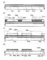
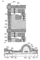
図29(A)は本発明に係る表示パネルの構成を示す上面図であり、絶縁表面を有する基板2700上に画素2702をマトリクス上に配列させた画素部2701、走査線側入力端子2703、信号線側入力端子2704が形成されている。画素数は種々の規格に従って設ければ良く、XGAであれば1024×768×3(RGB)、UXGAであれば1600×1200×3(RGB)、フルスペックハイビジョンに対応させるのであれば1920×1080×3(RGB)とすれば良い。
FIG. 29A is a top view illustrating a structure of a display panel according to the present invention. A
画素2702は、走査線側入力端子2703から延在する走査線と、信号線側入力端子2704から延在する信号線とが交差することで、マトリクス状に配設される。画素2702のそれぞれには、スイッチング素子とそれに接続する画素電極が備えられている。スイッチング素子の代表的な一例はTFTであり、TFTのゲート電極側が走査線と、ソース若しくはドレイン側が信号線と接続されることにより、個々の画素を外部から入力する信号によって独立して制御可能としている。
The
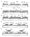
図33(A)は、走査線及び信号線へ入力する信号を、外付けの駆動回路により制御する表示パネルの構成を示しているが、図34(A)に示すように、COG(Chip on Glass)方式によりドライバIC2751を基板2700上に実装しても良い。また他の実装形態として、図34(B)に示すようなTAB(Tape Automated Bonding)方式を用いてもよい。ドライバICは単結晶半導体基板に形成されたものでも良いし、ガラス基板上にTFTで回路を形成したものであっても良い。図34において、ドライバIC2751は、FPC2750と接続している。
FIG. 33A shows a structure of a display panel in which signals input to the scanning lines and the signal lines are controlled by an external driver circuit. As shown in FIG. 34A, a COG (Chip on The
また、画素に設けるTFTをSASで形成する場合には、図33(B)に示すように走査線側駆動回路3702を基板3700上に形成し一体化することもできる。図34(B)において、3701は画素部であり、信号線側駆動回路は、図33(A)と同様に外付けの駆動回路により制御する。本発明で形成するTFTのように、画素に設けるTFTを移動度の高い、多結晶(微結晶)半導体、単結晶半導体などで形成する場合は、図33(C)は、走査線駆動回路4702と、信号線駆動回路4704をガラス基板4700上に一体形成することもできる。
In the case where a TFT provided for a pixel is formed using SAS, a scan
本発明は、配線層若しくは電極を形成する導電層や、所定のパターンに形成するためのマスク層など表示パネルを作製するために必要な物体(その目的や機能に応じて膜や層などあらゆる形態で存在する)のうち、少なくとも一つ若しくはそれ以上を、選択的に所望な形状にを形成可能な方法により形成して、表示装置を作製することを特徴とするものである。本発明は、薄膜トランジスタや表示装置を構成する、ゲート電極層、ソース電極層、ドレイン電極層などの導電層、半導体層、マスク層、絶縁層など、所定の形状を有して形成される全ての構成要素に対して適用できる。選択的に所望な形状に形成可能な方法として、導電層や絶縁層など形成し、特定の目的に調合された組成物の液滴を選択的に吐出(噴出)して所定のパターンに形成することが可能な、液滴吐出(噴出)法(その方式によっては、インクジェット法とも呼ばれる。)を用いる。また、物体が所望のパターンに転写、または描写できる方法、例えば各種印刷法(スクリーン(孔版)印刷、オフセット(平版)印刷、凸版印刷やグラビア(凹版)印刷など所望なパターンで形成される方法)なども用いることができる。 The present invention relates to an object necessary for manufacturing a display panel such as a conductive layer for forming a wiring layer or an electrode or a mask layer for forming a predetermined pattern (all forms such as a film and a layer depending on its purpose and function). The display device is manufactured by forming at least one or more of them in a method that can be selectively formed into a desired shape. The present invention includes all conductive layers such as a gate electrode layer, a source electrode layer, and a drain electrode layer, a semiconductor layer, a mask layer, an insulating layer, and the like that constitute a thin film transistor and a display device. Applicable to components. As a method that can be selectively formed into a desired shape, a conductive layer, an insulating layer, or the like is formed, and droplets of a composition prepared for a specific purpose are selectively ejected (ejected) to form a predetermined pattern. It is possible to use a droplet discharge (ejection) method (also called an ink jet method depending on the method). In addition, a method in which an object can be transferred or drawn in a desired pattern, for example, various printing methods (a method in which a desired pattern such as screen (stencil) printing, offset (flat plate) printing, relief printing or gravure (intaglio printing) is formed) Etc. can also be used.
本実施の形態は、流動性を有する形成する材料を含む組成物を、液滴として吐出(噴出)し、所望なパターンに形成する方法を用いている。形成物の被形成領域に、形成する材料を含む液滴を吐出し、焼成、乾燥等を行って固定化し所望なパターンで物体を形成する。 This embodiment mode uses a method in which a composition containing a material having fluidity is ejected (ejected) as droplets to form a desired pattern. A droplet containing a material to be formed is ejected onto a formation region of the formed product, and fixed by firing, drying, or the like to form an object with a desired pattern.
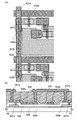
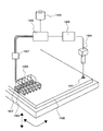
液滴吐出法に用いる液滴吐出装置の一態様を図31に示す。液滴吐出手段1403の個々のヘッド1405、ヘッド1412は制御手段1407に接続され、それがコンピュータ1410で制御することにより予めプログラミングされたパターンに描画することができる。描画するタイミングは、例えば、基板1400上に形成されたマーカー1411を基準に行えば良い。或いは、基板1400の縁を基準にして基準点を確定させても良い。これを撮像手段1404で検出し、画像処理手段1409にてデジタル信号に変換したものをコンピュータ1410で認識して制御信号を発生させて制御手段1407に送る。撮像手段1404としては、電荷結合素子(CCD)や相補型金属酸化物半導体(CMOS)を利用したイメージセンサなどを用いることができる。勿論、基板1400上に形成されるべきパターンの情報は記憶媒体1408に格納されたものであり、この情報を基にして制御手段1407に制御信号を送り、液滴吐出手段1403の個々のヘッド1405、ヘッド1412を個別に制御することができる。
One mode of a droplet discharge apparatus used for the droplet discharge method is shown in FIG. The individual heads 1405 and 1412 of the droplet discharge means 1403 are connected to the control means 1407, which can be drawn in a pre-programmed pattern under the control of the
ヘッド1405とヘッド1412のノズルのサイズは異なっており、異なる材料を異なる幅で同時に描画することができる。一つのヘッドで、導電性材料や有機、無機材料などをそれぞれ吐出し、描画することができ、層間膜のような広領域に描画する場合は、スループットを向上させるため複数のノズルより同材料を同時に吐出し、描画することができる。大型基板を用いる場合、ヘッド1405、ヘッド1412は基板上を、矢印の方向に自在に走査し、描画する領域を自由に設定することができ、同じパターンを一枚の基板に複数描画することができる。
The nozzle sizes of the
本発明では、形成物のパターニング工程においてを感光性のレジストや感光性物質を含む材料に光を照射し、露光する工程を行う。露光に用いる光は、特に限定されず、赤外光、可視光、または紫外光のいずれか一またはそれらの組み合わせを用いることが可能である。例えば、紫外線ランプ、ブラックライト、ハロゲンランプ、メタルハライドランプ、キセノンアークランプ、カーボンアークランプ、高圧ナトリウムランプ、または高圧水銀ランプから射出された光を用いてもよい。その場合、ランプ光源は、必要な時間点灯させて照射してもよいし、複数回照射してもよい。 In the present invention, in the patterning process of the formed product, a light exposure is performed by irradiating light to a photosensitive resist or a material containing a photosensitive substance. The light used for exposure is not particularly limited, and any one of infrared light, visible light, ultraviolet light, or a combination thereof can be used. For example, light emitted from an ultraviolet lamp, black light, halogen lamp, metal halide lamp, xenon arc lamp, carbon arc lamp, high pressure sodium lamp, or high pressure mercury lamp may be used. In that case, the lamp light source may be lit and irradiated for a necessary time, or may be irradiated multiple times.
レーザ光を用いてもよく、レーザ光を用いるとより精密なパターンで被形成領域を露光処理できるので、そこに形成される物体も高繊細化することができる。本発明で用いることのできるレーザ光(レーザビームともいう)を処理領域に描画する、レーザ光描画装置について、図50を用いて説明する。本実施の形態では、レーザ光を照射する領域をマスク等を介して選択するのではなく、処理領域を選択して直接照射して処理するため、レーザ光直接描装置を用いる。図50に示すようにレーザ光直接描画装置1001は、レーザ光を照射する際の各種制御を実行するパーソナルコンピュータ(以下、PCと示す。)1002と、レーザ光を出力するレーザ発振器1003と、レーザ発振器1003の電源1004と、レーザ光を減衰させるための光学系(NDフィルタ)1005と、レーザ光の強度を変調するための音響光学変調器(AOM)1006と、レーザ光の断面の拡大又は縮小をするためのレンズ、光路の変更するためのミラー等で構成される光学系1007、Xステージ及びYステージを有する基板移動機構1009と、PC1002から出力される制御データをデジタルーアナログ変換するD/A変換部1010と、D/A変換部から出力されるアナログ電圧に応じて音響光学変調器1006を制御するドライバ1011と、基板移動機構1009を駆動するための駆動信号を出力するドライバ1012とを備えている。
Laser light may be used, and when the laser light is used, the region to be formed can be exposed with a more precise pattern, so that an object formed there can also be highly fine. A laser beam drawing apparatus that draws laser light (also referred to as a laser beam) that can be used in the present invention in a processing region will be described with reference to FIG. In this embodiment, a laser beam direct drawing apparatus is used in order to select a processing region and directly irradiate and process it instead of selecting a region to be irradiated with laser light through a mask or the like. As shown in FIG. 50, a laser beam
レーザ発振器1003としては、紫外光、可視光、又は赤外光を発振することが可能なレーザ発振器を用いることができる。レーザー発振器としては、KrF、ArF、KrF、XeCl、Xe等のエキシマレーザ発振器、He、He−Cd、Ar、He−Ne、HF等の気体レーザ発振器、YAG、GdVO4、YVO4、YLF、YAlO3などの結晶にCr、Nd、Er、Ho、Ce、Co、Ti又はTmをドープした結晶を使った固体レーザー発振器、GaN、GaAs、GaAlAs、InGaAsP等の半導体レーザ発振器を用いることができる。なお、固体レーザ発振器においては、基本波の第1高調波〜第5高調波を適用するのが好ましい。
As the
次に、レーザ光直接描画装置を用いた物質(表面)の露光処理について述べる。基板1008が基板移動機構1009に装着されると、PC1002は図外のカメラによって、基板に付されているマーカの位置を検出する。次いで、PC1002は、検出したマーカの位置データと、予め入力されている描画パターンデータとに基づいて、基板移動機構1009を移動させるための移動データを生成する。この後、PC1002が、ドライバ1011を介して音響光学変調器1006の出力光量を制御することにより、レーザ発振器1003から出力されたレーザ光は、光学系1005によって減衰された後、音響光学変調器1006によって所定の光量になるように光量が制御される。一方、音響光学変調器1006から出力されたレーザ光は、光学系1007で光路及びレーザ光(ビームスポット)の形状を変化させ、レンズで集光した後、基板上に形成された被処理物に該レーザ光を照射して、被処理物を改質処理する。このとき、PC1002が生成した移動データに従い、基板移動機構1009をX方向及びY方向に移動制御する。この結果、所定の場所にレーザ光が照射され、被処理物の露光処理が行われる。
Next, a substance (surface) exposure process using a laser beam direct drawing apparatus will be described. When the
この結果、レーザ光が照射された領域で、被処理物は露光され、感光される。感光性物質には大きくわけてネガ型とポジ型がある。ネガ型の場合は、露光された部分で化学反応が生じ、現像液によって化学反応が生じた部分のみが残されてパターンが形成される。また、ポジ型の場合は、露光された部分で化学反応が生じ、現像液によって化学反応が生じた部分が溶解され、露光されなかった部分のみが残されてパターンが形成される。レーザ光のエネルギーの一部は被処理物材料で熱に変換され、被処理物の一部を反応させるため、処理された被処理物の領域の幅が、処理するレーザ光の幅より若干大きくなることもある。また、短波長のレーザ光ほど、レーザ光の径を短く集光することが可能であるため、微細な幅に処理領域を形成するためには、短波長のレーザ光を照射することが好ましい。 As a result, the workpiece is exposed and exposed in the region irradiated with the laser beam. Photosensitive materials are roughly divided into negative types and positive types. In the case of the negative type, a chemical reaction occurs in the exposed part, and only the part in which the chemical reaction is caused by the developer is left to form a pattern. In the case of the positive type, a chemical reaction occurs in the exposed portion, the portion in which the chemical reaction has occurred is dissolved by the developing solution, and only the unexposed portion is left to form a pattern. A part of the energy of the laser beam is converted into heat by the material to be processed, and a part of the object to be processed reacts. Therefore, the width of the processed object region is slightly larger than the width of the laser beam to be processed. Sometimes. Further, the shorter the wavelength of the laser light, the shorter the diameter of the laser light can be condensed. Therefore, it is preferable to irradiate the laser light with a short wavelength in order to form a processing region with a fine width.
また、レーザ光の膜表面でのスポット形状は、点状、円形、楕円形、矩形、または線状(厳密には細長い長方形状)となるように光学系で加工されている。 The spot shape on the film surface of the laser beam is processed by an optical system so as to be a dot, circle, ellipse, rectangle, or line (strictly, a long and narrow rectangle).
また、図50に示した装置は、基板の表面側からレーザー光を照射して露光する例を示したが、光学系や基板移動機構を適宜変更し、基板の裏面側からレーザー光を照射して露光するレーザビーム描画装置としてもよい。 50 shows an example in which exposure is performed by irradiating a laser beam from the front surface side of the substrate. However, the optical system and the substrate moving mechanism are appropriately changed to irradiate the laser beam from the back surface side of the substrate. Alternatively, a laser beam drawing apparatus that performs exposure may be used.
なお、ここでは、基板を移動して選択的にレーザ光を照射しているが、これに限定されず、レーザ光をX−Y軸方向に走査してレーザ光を照射することができる。この場合、光学系1007にポリゴンミラーやガルバノミラーを用いることが好ましい。
Note that here, the laser beam is selectively irradiated by moving the substrate, but the present invention is not limited to this, and the laser beam can be irradiated by scanning the laser beam in the X-Y axis direction. In this case, it is preferable to use a polygon mirror or a galvanometer mirror for the
また、光は、ランプ光源による光とレーザ光とを組み合わせて用いることもでき、比較的広範囲なパターニングを行う領域は、マスクを用いてランプによる照射処理を行い、高繊細なパターニングを行う領域のみレーザ光で照射処理を行うこともできる。このように光の照射処理を行うと、スループットも向上でき、かつ高繊細にパターニングされた配線基板などを得ることができる。 In addition, light can also be used in combination with light from a lamp light source and laser light, and the only area where patterning is relatively wide is to perform irradiation with a lamp using a mask to perform high-definition patterning. Irradiation treatment can also be performed with laser light. By performing the light irradiation treatment in this way, it is possible to improve the throughput and obtain a highly finely patterned wiring board or the like.
本発明の実施の形態について、図1乃至図8を用いて説明する。より詳しくは、本発明を適用した表示装置の作製方法について説明する。まず、本発明を適用した、チャネルエッチ型の薄膜トランジスタを有する表示装置の作製方法について説明する。図2〜図6(A)は表示装置画素部の上面図であり、図2〜図6の(B)は、図2〜図6(A)における線A―Cによる断面図、図2〜図6の(C)は、図2〜図6(A)における線B−Dによる断面図である。 Embodiment Modes of the present invention will be described with reference to FIGS. More specifically, a method for manufacturing a display device to which the present invention is applied will be described. First, a method for manufacturing a display device having a channel-etched thin film transistor to which the present invention is applied will be described. 2 to 6A are top views of the pixel portion of the display device, and FIG. 2B to FIG. 6B are cross-sectional views taken along line A—C in FIG. 2 to FIG. FIG. 6C is a cross-sectional view taken along line B-D in FIGS.
基板100は、バリウムホウケイ酸ガラス、アルミノホウケイ酸ガラス等からなるガラス基板、石英基板、シリコン基板、金属基板、ステンレス基板又は本作製工程の処理温度に耐えうる耐熱性を有するプラスチック基板を用いる。また、基板100の表面が平坦化されるようにCMP法などによって、研磨しても良い。なお、基板100上に、絶縁層を形成してもよい。絶縁層は、CVD法、プラズマCVD法、スパッタリング法、スピンコート法等の公知の方法により、珪素を含む酸化物材料、窒化物材料を用いて、単層又は積層して形成される。基板100として、320mm×400mm、370mm×470mm、550mm×650mm、600mm×720mm、680mm×880mm、1000mm×1200mm、1100mm×1250mm、1150mm×1300mmのような大面積基板を用いることができる。
As the
基板100上に、下地膜として絶縁層140を形成することが好ましい。この絶縁層140は、基板100からの汚染物質などを遮断する効果がある。基板100の上に下地膜として、絶縁層140をスパッタリング法、PVD法(Physical Vapor Deposition)、減圧CVD法(LPCVD法)、またはプラズマCVD法等のCVD法(Chemical Vapor Deposition)、スピンコート法等などにより珪素を含む酸化物材料、窒化物材料を用いて、単層又は積層して形成する。本実施の形態では、プラズマCVD法を用いて、窒化酸化珪素(SiNO)膜を10〜200nm(好ましくは50〜100nm)形成し、酸化窒化珪素(SiON)膜を50〜200nm(好ましくは100〜150nm)積層する。
An insulating
絶縁層としては、酸化珪素(SiOx)、窒化珪素(SiNx)、酸化窒化珪素(SiOxNy)(x>y)、窒化酸化珪素(SiNxOy)(x>y)などを用いることができ、単層でも2層、3層といった積層構造でもよい。なお本明細書中において酸化窒化珪素とは酸素の組成比が窒素の組成比より大きい物質(SiOxNy)(x>y)であり、窒素を含む酸化珪素とも言える。同様に、窒化酸化珪素とは、窒素の組成比が酸素の組成比より大きい物質(SiNxOy)(x>y)であり、酸素を含む窒化珪素とも言える。本実施の形態では、基板上にSiH4、NH3、N2O、N2及びH2を反応ガスとして窒化酸化珪素膜を膜厚50nm形成し、SiH4及びN2Oを反応ガスとして酸化窒化珪素膜を膜厚100nmで形成する。また窒化酸化珪素膜の膜厚を140nm、積層する酸化窒化珪素膜の膜厚を100nmとしてもよい。 As the insulating layer, silicon oxide (SiOx), silicon nitride (SiNx), silicon oxynitride (SiOxNy) (x> y), silicon nitride oxide (SiNxOy) (x> y), or the like can be used. A laminated structure of two layers or three layers may be used. Note that in this specification, silicon oxynitride is a substance (SiOxNy) (x> y) in which the composition ratio of oxygen is higher than the composition ratio of nitrogen, and can also be referred to as silicon oxide containing nitrogen. Similarly, silicon nitride oxide is a substance (SiNxOy) (x> y) in which the composition ratio of nitrogen is higher than the composition ratio of oxygen, and can be said to be silicon nitride containing oxygen. In this embodiment, a silicon nitride oxide film having a thickness of 50 nm is formed on a substrate using SiH 4 , NH 3 , N 2 O, N 2, and H 2 as reactive gases, and oxidized using SiH 4 and N 2 O as reactive gases. A silicon nitride film is formed with a thickness of 100 nm. The thickness of the silicon nitride oxide film may be 140 nm, and the thickness of the stacked silicon oxynitride film may be 100 nm.
絶縁層140上に導電膜101を形成する。導電膜101は、パターニングされソース電極層又はドレイン電極層と、画素電極層として機能する第1の電極層とになる。導電膜101は、印刷法、電界メッキ法、PVD法(Physical Vapor Deposition)、CVD法(Chemical Vapor Deposition)、蒸着法等の公知の手法により高融点材料を用いて形成することが好ましい。また形成方法としては、液滴吐出法によって所望のパターンに形成することもできる。高融点材料を用いることにより、後の加熱工程が可能となる。高融点材料としては、タングステン(W)、モリブデン(Mo)、ジルコニア(Zr)、ハフニウム(Hf)、ビスマス(V)、ニオブ(Nb)、タンタル(Ta)、クロム(Cr)、コバルト(Co)、ニッケル(Ni)、白金(Pt)等の金属又はその合金、若しくはその金属窒化物を適宜用いることができる。また、これら複数の層を積層して形成しても良い。代表的には、基板表面に窒化タンタル膜、その上にタングステン膜を積層してもよい。なお、後の加熱工程が、ハロゲンランプ、メタルハライドランプ、キセノンアークランプ、カーボンアークランプ、高圧ナトリウムランプ、高圧水銀ランプから選ばれた一種または複数種からの輻射により行うLRTA(Lamp Rapid Thermal Anneal)法、窒素やアルゴンなどの不活性気体を加熱媒質として用いるGRTA(Gas Rapid Thermal Anneal)法を用いる場合、短時間による熱処理のため比較的融点の低いアルミニウム(Al)、銀(Ag)、金(Cu)を用いて導電膜を形成しても良い。このような反射性を有する金属は、上面放射型の表示装置を作製する場合には好ましい。また、珪素に一導電型を付与する不純物元素を添加した材料を用いても良い。例えば、非晶質珪素膜にリン(P)などのn型を付与する不純物元素が含まれたn型を有する珪素膜などを用いることができる。
A
導電膜101は、画素電極層としても機能するので、透明導電性材料を用いて形成することもできる。画素電極層となる第1の電極層は、インジウム錫酸化物(ITO)、酸化珪素を含むインジウム錫酸化物(ITSO)、酸化亜鉛(ZnO)、酸化スズ(SnO2)などにより形成してもよい。好ましくは、スパッタリング法によりインジウム錫酸化物(ITO)、酸化珪素を含むインジウム錫酸化物(ITSO)、酸化亜鉛(ZnO)などで形成する。より好ましくは、ITOに酸化珪素が2〜10重量%含まれたターゲットを用いてスパッタリング法で酸化珪素を含む酸化インジウムスズを用いる。この他、酸化珪素を含み酸化インジウムに2〜20%の酸化亜鉛(ZnO)を混合した酸化インジウム酸化亜鉛合金などの導電性材料を用いても良い。
Since the
本実施の形態では、導電膜101は、導電性材料としてインジウム錫酸化物を含む組成物を吐出して、550℃で焼成し、導電膜101を形成する。液滴吐出手段とは、組成物の吐出口を有するノズルや、1つ又は複数のノズルを具備したヘッド等の液滴を吐出する手段を有するものの総称とする。液滴吐出手段が具備するノズルの径は、0.02〜100μm(好適には30μm以下)に設定し、該ノズルから吐出される組成物の吐出量は0.001pl〜100pl(好適には0.1pl以上40pl以下、より好ましくは10pl以下)に設定する。吐出量は、ノズルの径の大きさに比例して増加する。また、被処理物とノズルの吐出口との距離は、所望の箇所に滴下するために、出来る限り近づけておくことが好ましく、好適には0.1〜3mm(好適には1mm以下)程度に設定する。
In this embodiment, the
吐出口から吐出する組成物は、導電性材料を溶媒に溶解又は分散させたものを用いる。導電性材料とは、Ag、Au、Cu、Ni、Pt、Pd、Ir、Rh、W、Al等の金属、Cd、Znの金属硫化物、Fe、Ti、Si、Ge、Si、Zr、Baなどの酸化物、ハロゲン化銀の微粒子又は分散性ナノ粒子に相当する。また、透明導電膜として用いられるインジウム錫酸化物(ITO)、インジウム錫酸化物と酸化珪素からなるITSO、有機インジウム、有機スズ、酸化亜鉛、窒化チタン等に相当する。但し、吐出口から吐出する組成物は、比抵抗値を考慮して、金、銀、銅のいずれかの材料を溶媒に溶解又は分散させたものを用いることが好適であり、より好適には、低抵抗な銀、銅を用いるとよい。但し、銀、銅を用いる場合には、不純物対策のため、合わせてバリア膜を設けるとよい。バリア膜としては、窒化珪素膜やニッケルボロン(NiB)を用いるとことができる。 A composition in which a conductive material is dissolved or dispersed in a solvent is used as the composition discharged from the discharge port. Conductive materials include metals such as Ag, Au, Cu, Ni, Pt, Pd, Ir, Rh, W, and Al, metal sulfides of Cd, Zn, Fe, Ti, Si, Ge, Si, Zr, Ba It corresponds to oxides such as silver halide fine particles or dispersible nanoparticles. Further, it corresponds to indium tin oxide (ITO) used as a transparent conductive film, ITSO composed of indium tin oxide and silicon oxide, organic indium, organic tin, zinc oxide, titanium nitride, and the like. However, it is preferable to use a composition in which any of gold, silver and copper is dissolved or dispersed in a solvent in consideration of the specific resistance value, more preferably the composition discharged from the discharge port. It is preferable to use low resistance silver or copper. However, when silver or copper is used, a barrier film may be provided as a countermeasure against impurities. As the barrier film, a silicon nitride film or nickel boron (NiB) can be used.
また、導電性材料の周りに他の導電性材料がコーティングされ、複数の層になっている粒子でも良い。例えば、銅の周りにニッケルボロン(NiB)がコーティングされ、その周囲に銀がコーティングされている3層構造の粒子などを用いても良い。溶媒は、酢酸ブチル、酢酸エチル等のエステル類、イソプロピルアルコール、エチルアルコール等のアルコール類、メチルエチルケトン、アセトン等の有機溶剤等を用いる。組成物の粘度は20mPa・s(cps)以下が好適であり、これは、乾燥が起こることを防止したり、吐出口から組成物を円滑に吐出できるようにしたりするためである。また、組成物の表面張力は、40mN/m以下が好適である。但し、用いる溶媒や、用途に合わせて、組成物の粘度等は適宜調整するとよい。一例として、ITOや、有機インジウム、有機スズを溶媒に溶解又は分散させた組成物の粘度は5〜20mPa・s、銀を溶媒に溶解又は分散させた組成物の粘度は5〜20mPa・s、金を溶媒に溶解又は分散させた組成物の粘度は5〜20mPa・sに設定するとよい。 Alternatively, particles in which a conductive material is coated with another conductive material to form a plurality of layers may be used. For example, particles having a three-layer structure in which nickel boron (NiB) is coated around copper and silver is coated around it may be used. As the solvent, esters such as butyl acetate and ethyl acetate, alcohols such as isopropyl alcohol and ethyl alcohol, organic solvents such as methyl ethyl ketone and acetone are used. The composition preferably has a viscosity of 20 mPa · s (cps) or less, in order to prevent drying from occurring or to smoothly discharge the composition from the discharge port. The surface tension of the composition is preferably 40 mN / m or less. However, the viscosity and the like of the composition may be appropriately adjusted according to the solvent to be used and the application. As an example, the viscosity of a composition in which ITO, organic indium, or organic tin is dissolved or dispersed in a solvent is 5 to 20 mPa · s, the viscosity of a composition in which silver is dissolved or dispersed in a solvent is 5 to 20 mPa · s, The viscosity of the composition in which gold is dissolved or dispersed in a solvent is preferably set to 5 to 20 mPa · s.
また、電極層となる導電膜101は、複数の導電性材料を積層しても良い。また、始めに導電性材料として銀を用いて、液滴吐出法で導電層を形成した後、銅などでめっきを行ってもよい。めっきは電気めっきや化学(無電界)めっき法で行えばよい。めっきは、めっきの材料を有する溶液を満たした容器に基板表面を浸してもよいが、基板を斜め(または垂直)に立てて設置し、めっきする材料を有する溶液を、基板表面に流すように塗布してもよい。基板を立てて溶液を塗布するようにめっきを行うと、工程装置が小型化する利点がある。
Further, the
各ノズルの径や所望のパターン形状などに依存するが、ノズルの目詰まり防止や高精細なパターンの作製のため、導電体の粒子の径はなるべく小さい方が好ましく、好適には粒径0.1μm以下が好ましい。組成物は、電解法、アトマイズ法又は湿式還元法等の公知の方法で形成されるものであり、その粒子サイズは、一般的に約0.01〜10μmである。但し、ガス中蒸発法で形成すると、分散剤で保護されたナノ分子は約7nmと微細であり、またこのナノ粒子は、被覆剤を用いて各粒子の表面を覆うと、溶剤中に凝集がなく、室温で安定に分散し、液体とほぼ同じ挙動を示す。従って、被覆剤を用いることが好ましい。 Although depending on the diameter of each nozzle and the desired pattern shape, the diameter of the conductor particles is preferably as small as possible for preventing nozzle clogging and producing a high-definition pattern. 1 μm or less is preferable. The composition is formed by a known method such as an electrolytic method, an atomizing method, or a wet reduction method, and its particle size is generally about 0.01 to 10 μm. However, when formed in a gas evaporation method, the nanomolecules protected with the dispersant are as fine as about 7 nm. When the surface of each particle is covered with a coating agent, the nanoparticles are aggregated in the solvent. And stably disperse at room temperature and shows almost the same behavior as liquid. Therefore, it is preferable to use a coating agent.
組成物を吐出する工程は、減圧下で行うと、組成物を吐出して被処理物に着弾するまでの間に、該組成物の溶媒が揮発し、後の乾燥と焼成の工程を省略することができる。また、減圧下で行うと、導電体の表面に酸化膜などが形成されないため好ましい。また、組成物を吐出後、乾燥と焼成の一方又は両方の工程を行う。乾燥と焼成の工程は、両工程とも加熱処理の工程であるが、例えば、乾燥は100度で3分間程度の数分間、焼成は200〜350度で15分間〜60分間で行うもので、その目的、温度と時間が異なるものである。乾燥の工程、焼成の工程は、常圧下又は減圧下で、レーザ光の照射や瞬間熱アニール、加熱炉などにより行う。なお、この加熱処理を行うタイミングは特に限定されない。乾燥と焼成の工程を良好に行うためには、基板を加熱しておいてもよく、そのときの温度は、基板等の材質に依存するが、一般的には100〜800度(好ましくは200〜350度)とする。本工程により、組成物中の溶媒の揮発、又は化学的に分散剤を除去するとともに、周囲の樹脂が硬化収縮することで、ナノ粒子間を接触させ、融合と融着を加速する。 When the step of discharging the composition is performed under reduced pressure, the solvent of the composition is volatilized between the time of discharging the composition and landing on the object to be processed, and the subsequent drying and baking steps are omitted. be able to. Further, it is preferable to perform under reduced pressure because an oxide film or the like is not formed on the surface of the conductor. In addition, after discharging the composition, one or both steps of drying and baking are performed. The drying and firing steps are both heat treatment steps. For example, drying is performed at 100 degrees for about 3 minutes for several minutes, and firing is performed at 200 to 350 degrees for 15 minutes to 60 minutes. Purpose, temperature and time are different. The drying process and the firing process are performed under normal pressure or reduced pressure by laser light irradiation, rapid thermal annealing, a heating furnace, or the like. In addition, the timing which performs this heat processing is not specifically limited. In order to satisfactorily perform the drying and firing steps, the substrate may be heated, and the temperature at that time depends on the material of the substrate or the like, but is generally 100 to 800 degrees (preferably 200). ~ 350 degrees). By this step, the solvent in the composition is volatilized or the dispersant is chemically removed, and the surrounding resin is cured and contracted to bring the nanoparticles into contact with each other, thereby accelerating fusion and fusion.
レーザ光の照射は、連続発振またはパルス発振の気体レーザ又は固体レーザを用いれば良い。前者の気体レーザとしては、エキシマレーザ、YAGレーザ等が挙げられ、後者の固体レーザとしては、Cr、Nd等がドーピングされたYAG、YVO4、GdVO4等の結晶を使ったレーザ等が挙げられる。なお、レーザ光の吸収率の関係から、連続発振のレーザを用いることが好ましい。また、パルス発振と連続発振を組み合わせた所謂ハイブリッドのレーザ照射方法を用いてもよい。但し、基板100の耐熱性に依っては、レーザ光の照射による加熱処理は、該基板100が破壊しないように、数マイクロ秒から数十秒の間で瞬間的に行うとよい。瞬間熱アニール(RTA)は、不活性ガスの雰囲気下で、紫外光乃至赤外光を照射する赤外ランプやハロゲンランプなどを用いて、急激に温度を上昇させ、数分〜数マイクロ秒の間で瞬間的に熱を加えて行う。この処理は瞬間的に行うために、実質的に最表面の薄膜のみを加熱することができ、下層の膜には影響を与えない。つまり、プラスチック基板等の耐熱性が弱い基板にも影響を与えない。
For the laser light irradiation, a continuous wave or pulsed gas laser or solid-state laser may be used. Examples of the former gas laser include an excimer laser and a YAG laser, and examples of the latter solid-state laser include a laser using a crystal such as YAG, YVO 4 or GdVO 4 doped with Cr, Nd, or the like. . Note that it is preferable to use a continuous wave laser because of the absorption rate of the laser light. In addition, a so-called hybrid laser irradiation method combining pulse oscillation and continuous oscillation may be used. However, depending on the heat resistance of the
また、液滴吐出法により、導電膜101を組成物を吐出し形成した後、その平坦性を高めるために表面を圧力によってプレスして平坦化してもよい。プレスの方法としては、ローラー状のものを表面に走査することによって、凹凸をならすように軽減したり、平坦な板状な物で表面を垂直にプレスしてもよい。プレスする時に、加熱工程を行っても良い。また溶剤等によって表面を軟化、または融解させエアナイフで表面の凹凸部を除去しても良い。また、CMP法を用いて研磨しても良い。この工程は、液滴吐出法によって凹凸が生じる場合に、その表面の平坦化する場合適用することができる。また、平坦化の工程は、マスク102a、マスク102b、マスク102c、マスク102d、マスク102eによって導電膜101がパターニングされ、ソース電極層又はドレイン電極層103、ソース電極層又はドレイン電極層104、ソース電極層又はドレイン電極層105、ソース電極層又はドレイン電極層106、第1の電極層107が形成された後行っても良い。
Alternatively, after the
本実施の形態では、工程を簡略化するため、導電膜101上に、一導電型を有する半導体膜201a及び一導電型を有する半導体膜201bを積層した後、導電膜101、一導電型を有する半導体膜201a及び一導電型を有する半導体膜201bを同時にエッチングし、パターニングする。一導電型を有する半導体膜201a及び一導電型を有する半導体膜201bは、ソース領域又はドレイン領域として機能する。
In this embodiment, in order to simplify the process, after the
本実施の形態では、プラズマCVD法を用いて、一導電型を有する半導体層である一導電型を有する半導体膜201a、一導電型を有する半導体膜201bを形成する。一導電型を有する半導体膜201aの膜厚は、20〜200nm(代表的には50〜150nm)、一導電型を有する半導体膜201bの膜厚は、30〜100nm(代表的には40〜60nm)とする。一導電型を有する半導体膜201a、一導電型を有する半導体膜201bは不純物元素を有しており、不純物元素としてはn型を付与する不純物元素、p型を付与する不純物元素を用いることができ、例えばリン(P)、窒素(N)、ヒ素(As)、アンチモン(Sb)、ビスマス(Bi)、ボロン(B)から選ばれた一種または複数種を用いることができる。また一導電型を付与する不純物元素の他に希ガス元素を含むようにして形成しても良く、希ガス元素としてはヘリウム(He)、ネオン(Ne)、アルゴン(Ar)、Kr(クリプトン)、Xe(キセノン)から選ばれた一種または複数種を用いることができる。例えば、n型を付与する不純物元素としてリンを含むn型を有する半導体層に、アルゴンなどの希ガス元素が含まれるように形成することもできる。本実施の形態では、一導電型を有する半導体膜201aを一導電型を有する半導体膜201bには、n型を付与する不純物元素(本実施の形態ではリンを用いる)が含まれており、一導電型を有する半導体膜201bの不純物元素の濃度は、一導電型を有する半導体膜201aより低くなるように形成されている。前記不純物元素は、CVD法などによって、不純物元素を含むように半導体膜を形成しても良いし、半導体膜を形成後に、不純物元素をイオンドーピング法などによって添加してもよい。
In this embodiment, a
プラズマCVD法によりn型を付与する不純物元素が含まれる一導電型を有する半導体膜201aはn型の高濃度不純物領域(n+領域ともいう)として形成され、一導電型を有する半導体膜201bはn型の低濃度不純物領域(n−領域ともいう)として形成されている。よって一導電型を有する半導体膜201a、一導電型を有する半導体膜201bのそれぞれの膜において深さ方向に対して一定の濃度のn型を付与する不純物元素が分布しており、一導電型を有する半導体膜201aの方が、一導電型を有する半導体膜201bより高い濃度でn型を付与する不純物元素が分布している。n+領域である一導電型を有する半導体膜201aは後にソース領域及びドレイン領域として機能し、n−領域である一導電型を有する半導体膜201bはLDD(LightlyDoped Drain)領域として機能する。なお、n+領域とn−領域はそれぞれ作り分けているので界面が存在する。n+領域とn−領域の膜厚制御は、それぞれ各濃度の半導体膜の膜厚を制御することによって達成できる。
A
一方、半導体膜を形成し、イオンドープ法又はイオン注入法により該半導体膜にn型を付与する不純物元素を添加して一導電型を有する半導体膜を形成してもよい。この場合、そのドーピング条件によって一導電型を有する半導体膜中の不純物の濃度分布を制御すればよい。本実施の形態の一導電型を有する半導体膜201a及び一導電型を有する半導体膜201bのように、半導体膜の表面から膜厚方向に深い領域のn型を付与する不純物元素濃度が1×10¹⁹/cm3以上のn型の高濃度不純物領域(n+領域ともいう)とし、膜厚方向に浅い半導体膜の表面に近い領域をn型を付与する不純物元素濃度が5×1017〜1×1019/cm3のn型の低濃度不純物領域(n−領域ともいう)となるように形成する。n+領域は後にソース領域及びドレイン領域として機能し、n−領域はLDD領域として機能する。なお、n+領域とn−領域それぞれの界面は存在せず、相対的なn型を付与する不純物元素濃度の濃度の大小によって変化する。このようにイオンドープ法又はイオン注入法により形成されたn型を付与する不純物元素が含まれる一導電型を有する半導体膜の場合は、添加条件によって濃度プロファイルを制御し、n+領域とn−領域の膜厚を適宜制御することが可能である。n+領域とn−領域を有することにより電界の緩和効果が大きくなり、ホットキャリア耐性を高めた薄膜トランジスタを形成することが可能となる。
On the other hand, a semiconductor film may be formed, and an impurity element imparting n-type conductivity may be added to the semiconductor film by an ion doping method or an ion implantation method to form a semiconductor film having one conductivity type. In this case, the impurity concentration distribution in the semiconductor film having one conductivity type may be controlled according to the doping conditions. As in the
本実施の形態では、一導電型を有する半導体膜201a、一導電型を有する半導体膜201bとして、n型を付与する不純物元素(ドナー型元素)であるリンを含むn型を有する半導体膜をプラズマCVD法によって形成する。また、一導電型を有する半導体膜201a、一導電型を有する半導体膜201bに含まれるn型を付与する不純物元素の濃度を異ならせているので、一導電型を有する半導体膜201aはn型の高濃度不純物領域となり、一導電型を有する半導体膜201bはn型の低濃度不純物領域となっている。n型の低濃度不純物領域の不純物濃度は、1×10¹⁷〜3×10¹⁹/cm3、好ましくは1×1018〜1×1019/cm3、n型の高濃度不純物領域の不純物濃度は、その10倍から100倍が好ましく、1×1019〜3×1021/cm3とすることができる。n型の高濃度不純物領域である一導電型を有する半導体膜201aの膜厚は30〜100nm、代表的には40〜60nmであり、本実施の形態では、膜厚50nmで形成する。またn型の低濃度不純物領域である一導電型を有する半導体膜201bの膜厚は20〜200nm、代表的には50〜150nmであり、本実施の形態では、膜厚50nmで形成する。
In this embodiment, an n-type semiconductor film containing phosphorus which is an impurity element imparting n-type (donor-type element) is used as a plasma as the
導電膜101、一導電型を有する半導体膜201a、及び一導電型を有する半導体膜201bのパターニング工程を図7を用いて説明する。導電膜101をパターニングして形成するソース電極層又はドレイン電極層は、微細なパターンで設計されており、制御性よく形成しなければ形成不良によるショート等の不良を引き起こす。よって、導電膜及び一導電型を有する半導体層の微細なパターニングはレーザ光による微細な加工によって行う。図7(A)(B)で示すように、基板100上に絶縁層140、導電膜101、一導電型を有する半導体膜201a、一導電型を有する半導体膜201b上に、レジストからなるマスク230を形成する。マスク230も液滴吐出法を用いて形成することができる。液滴吐出法を組み合わせることで、スピンコート法などによる全面塗布形成に比べ、材料のロスが防げ、コストダウンが可能になる。
A patterning process of the
マスク230は、感光剤を含む市販のレジスト材料を用いてもよく、例えば、代表的なポジ型レジストである、ノボラック樹脂と感光剤であるナフトキノンジアジド化合物、ネガ型レジストであるベース樹脂、ジフェニルシランジオール及び酸発生剤などを用いてもよい。いずれの材料を用いるとしても、その表面張力と粘度は、溶媒の濃度を調整したり、界面活性剤等を加えたりして適宜調整する。
For the
レジストからなるマスク230に、レーザ光240a、レーザ光240b、レーザ光240cを照射し、露光することによって領域231a、領域231b、領域231cを感光する(図7(B)参照。)。レーザ光の照射は、複数のレーザ光を一度に照射して行っても良いし、レーザ光、または処理物を相対的に走査して照射を行っても良い。本実施の形態ではポジ型の感光性のレジストを用いるため、露光された領域231a、領域231b、領域231cはエッチャントによって除去され、開口部232a、開口部232b、開口部232cが形成される(図7(C)参照。)。マスク102a、マスク102b、マスク102cを用いて、導電膜101、一導電型を有する半導体膜201a、一導電型を有する半導体膜201bをエッチングによりパターニングすることによって、ソース電極層又はドレイン電極層103、ソース電極層又はドレイン電極層104、ソース電極層又はドレイン電極層105、一導電型を有する半導体層202a、一導電型を有する半導体層202b、一導電型を有する半導体層203a、一導電型を有する半導体層203b、一導電型を有する半導体層204a、一導電型を有する半導体層204bが形成される(図7(D)参照。)。
The resist
導電膜101、一導電型を有する半導体膜201a、一導電型を有する半導体膜201bのエッチング工程は、一回のエッチング工程で行っても良いし、複数のエッチング工程によって行っても良い。例えば、一導電型を有する半導体膜201a及び一導電型を有する半導体膜201bをエッチングした後、エッチングガスやエッチング条件を異ならせて導電膜101をエッチングしてもよい。この場合、一導電型を有する半導体膜201a及び一導電型を有する半導体膜201bと、導電膜101とのエッチングにおける選択比が大きければ、先にパターニングされた一導電型を有する半導体膜201a及び一導電型を有する半導体膜201bをマスクとして導電膜101をエッチングすることもできる。
The etching process of the
パターニングの際のエッチング加工は、プラズマエッチング(ドライエッチング)又はウエットエッチングのどちらを採用しても良い。大面積基板を処理するにはプラズマエッチングが適している。エッチングガスとしては、CF4、NF3、SF6、CHF3などのフッ素系又はCl2、BCl3、SiCl4もしくはCCl4などを代表とする塩素系ガス、あるいはO2のガスを用い、HeやArなどの不活性ガスを適宜加えても良い。また、大気圧放電のエッチング加工を適用すれば、局所的な放電加工も可能であり、基板の全面にマスク層を形成する必要はない。本実施の形態では、一導電型を有する半導体膜201a及び一導電型を有する半導体膜201bをドライエッチングによってエッチングし、導電膜101をエッチャントを用いるウエットエッチングによってエッチングする。
As the etching process at the time of patterning, either plasma etching (dry etching) or wet etching may be employed. Plasma etching is suitable for processing large area substrates. As an etching gas, a fluorine-based gas such as CF 4 , NF 3 , SF 6 , or CHF 3 , a chlorine-based gas typified by Cl 2 , BCl 3 , SiCl 4, CCl 4, or the like, or an O 2 gas is used. An inert gas such as Ar or Ar may be added as appropriate. Further, if an atmospheric pressure discharge etching process is applied, a local electric discharge process is also possible, and it is not necessary to form a mask layer on the entire surface of the substrate. In this embodiment, the
このようにレーザ光による微細な加工によりマスクを形成し、導電膜のパターニングを行うことで、制御性よく精密に導電膜をパターニングでき、所望な形状のソース電極層やドレイン電極層を形成することができる。よって形成不良が生じないために薄膜トランジスタの信頼性も向上する。また、導電膜101を基板全面に形成せず、液滴吐出法によって選択的に形成すれば、微細な加工のみをマスクを用いて行えばよいので、材料のロスも軽減し、工程も簡略化するため、コストが低く生産性が上がるという利点がある。
By forming a mask by fine processing with laser light and patterning the conductive film in this way, the conductive film can be patterned with high controllability and a desired shape of the source electrode layer and the drain electrode layer can be formed. Can do. Therefore, since the formation failure does not occur, the reliability of the thin film transistor is also improved. Further, if the
ソース電極層又はドレイン電極層、第1の電極層を形成するための導電膜101のパターニング工程を導電膜101の形成直後に行っても良い。この場合、導電膜101に感光性を有する感光性物質を含む導電性材料を用いると、レジストからなるマスクを形成しなくても導電膜101に直接レーザ光を照射し、露光、エッチャントによる除去を行うことで、所望のパターンにパターニングすることができる。この場合、マスクを形成せずともよいので工程が簡略化する利点がある。感光性物質を含む導電性材料は、Ag、Au、Cu、Ni、Al、Ptなどの金属或いは合金と、有機高分子樹脂、光重合開始剤、光重合単量体、または溶剤などからなる感光性樹脂とを含んだものを用いればよい。有機高分子樹脂としては、ノボラック樹脂、アクリル系コポリマー、メタクリル系コポリマー、セルローズ誘導体、環化ゴム系樹脂などを用いる。
The patterning step of the
このように微細に加工されたマスク102a、マスク102b、マスク102c、マスク102d、マスク102eを用いて導電膜101をパターニングし、ソース電極層又はドレイン電極層103、ソース電極層又はドレイン電極層104、ソース電極層又はドレイン電極層105、ソース電極層又はドレイン電極層106、及び画素電極層となる第1の電極層107、一導電型を有する半導体層202a、一導電型を有する半導体層202b、一導電型を有する半導体層203a、一導電型を有する半導体層203b、一導電型を有する半導体層204a、一導電型を有する半導体層204b、一導電型を有する半導体層205a、一導電型を有する半導体層205b、一導電型を有する半導体層206a、一導電型を有する半導体層206bを形成する(図3参照。)。
The
次に半導体膜を形成する。半導体層の詳細な作製方法を図8を用いて説明する。図8はソース電極層又はドレイン電極層103及びソース電極層又はドレイン電極層104上に形成される薄膜トランジスタの作製方法を示しているが、ソース電極層又はドレイン電極層105及びソース電極層又はドレイン電極層106上に形成される薄膜トランジスタも同様に作製することができる。半導体膜は25〜200nm(好ましくは30〜150nm)の厚さで公知の手段(スパッタ法、LPCVD法、またはプラズマCVD法等)により成膜すればよい。本実施の形態では、非晶質半導体膜を結晶化し、結晶性半導体膜とするものを用いるのが好ましい。
Next, a semiconductor film is formed. A detailed method for manufacturing the semiconductor layer will be described with reference to FIGS. FIG. 8 illustrates a method for manufacturing a thin film transistor formed over the source or drain
半導体膜を形成する材料は、シランやゲルマンに代表される半導体材料ガスを用いて気相成長法やスパッタリング法で作製される非晶質半導体(以下「アモルファス半導体:AS」ともいう。)、該非晶質半導体を熱エネルギーを利用して結晶化させた多結晶半導体、或いはセミアモルファス(微結晶若しくはマイクロクリスタルとも呼ばれる。以下「SAS」ともいう。)半導体などを用いることができる。 As a material for forming the semiconductor film, an amorphous semiconductor (hereinafter also referred to as “amorphous semiconductor: AS”) manufactured by a vapor deposition method or a sputtering method using a semiconductor material gas typified by silane or germane is used. A polycrystalline semiconductor obtained by crystallizing a crystalline semiconductor using thermal energy, a semi-amorphous (also referred to as microcrystal or microcrystal, hereinafter, also referred to as “SAS”) semiconductor, or the like can be used.
SASは、非晶質と結晶構造(単結晶、多結晶を含む)の中間的な構造を有し、自由エネルギー的に安定な第3の状態を有する半導体であって、短距離秩序を持ち格子歪みを有する結晶質な領域を含んでいる。少なくとも膜中の一部の領域には、0.5〜20nmの結晶領域を観測することが出来、珪素を主成分とする場合にはラマンスペクトルが520cm-1よりも低波数側にシフトしている。X線回折では珪素結晶格子に由来するとされる(111)、(220)の回折ピークが観測される。未結合手(ダングリングボンド)の中和剤として水素またはハロゲンを少なくとも1原子%またはそれ以上含ませている。SASは、珪化物気体をグロー放電分解(プラズマCVD)して形成する。珪化物気体としては、SiH4、その他にもSi2H6、SiH2Cl2、SiHCl3、SiCl4、SiF4などを用いることが可能である。またF2、GeF4を混合させても良い。この珪化物気体をH2、又は、H2とHe、Ar、Kr、Neから選ばれた一種または複数種の希ガス元素で希釈しても良い。希釈率は2〜1000倍の範囲、圧力は概略0.1Pa〜133Paの範囲、電源周波数は1MHz〜120MHz、好ましくは13MHz〜60MHzである。基板加熱温度は300℃以下が好ましく、100〜200℃の基板加熱温度でも形成可能である。ここで、主に成膜時に取り込まれる不純物元素として、酸素、窒素、炭素などの大気成分に由来する不純物は1×1020cm-3以下とすることが望ましく、特に、酸素濃度は5×1019cm-3以下、好ましくは1×1019cm-3以下となるようにすることが好ましい。また、ヘリウム、アルゴン、クリプトン、ネオンなどの希ガス元素を含ませて格子歪みをさらに助長させることで安定性が増し良好なSASが得られる。また半導体膜としてフッ素系ガスより形成されるSAS層に水素系ガスより形成されるSAS層を積層してもよい。 SAS is a semiconductor having an intermediate structure between amorphous and crystalline structures (including single crystal and polycrystal) and having a third state that is stable in terms of free energy and has a short-range order and a lattice. It includes a crystalline region with strain. A crystal region of 0.5 to 20 nm can be observed in at least a part of the film, and when silicon is the main component, the Raman spectrum shifts to a lower wave number side than 520 cm −1. Yes. In X-ray diffraction, diffraction peaks of (111) and (220) that are derived from the silicon crystal lattice are observed. At least 1 atomic% or more of hydrogen or halogen is contained as a neutralizing agent for dangling bonds. The SAS is formed by glow discharge decomposition (plasma CVD) of a silicide gas. As the silicide gas, SiH 4 , Si 2 H 6 , SiH 2 Cl 2 , SiHCl 3 , SiCl 4 , SiF 4, and the like can be used. Further, F 2 and GeF 4 may be mixed. This silicide gas may be diluted with H 2 , or H 2 and one or more kinds of rare gas elements selected from He, Ar, Kr, and Ne. The dilution rate is in the range of 2 to 1000 times, the pressure is in the range of approximately 0.1 Pa to 133 Pa, and the power supply frequency is 1 MHz to 120 MHz, preferably 13 MHz to 60 MHz. The substrate heating temperature is preferably 300 ° C. or lower, and can be formed even at a substrate heating temperature of 100 to 200 ° C. Here, as an impurity element mainly taken in at the time of film formation, it is desirable that impurities derived from atmospheric components such as oxygen, nitrogen, and carbon be 1 × 10 20 cm −3 or less, and in particular, the oxygen concentration is 5 × 10 5. It is preferable to be 19 cm −3 or less, preferably 1 × 10 19 cm −3 or less. Further, by adding a rare gas element such as helium, argon, krypton, or neon to further promote lattice distortion, stability is improved and a favorable SAS can be obtained. In addition, a SAS layer formed of a hydrogen-based gas may be stacked on a SAS layer formed of a fluorine-based gas as a semiconductor film.
なお、後の結晶化で良質な結晶構造を有する半導体膜を得るためには、図8に示す非晶質半導体膜436中に含まれる酸素、窒素などの不純物濃度を5×10¹⁸/cm3(以下、濃度はすべて二次イオン質量分析法(SIMS)にて測定した原子濃度として示す。)以下に低減させておくと良い。これらの不純物は、結晶化を促進させる金属元素と反応しやすく、後の結晶化を妨害する要因となり、また、結晶化後においても捕獲中心や再結合中心の密度を増加させる要因となる。
Note that in order to obtain a semiconductor film having a good crystal structure by subsequent crystallization, the concentration of impurities such as oxygen and nitrogen contained in the
本実施の形態では、非晶質半導体膜、又はSAS膜に結晶化を助長する元素を用いた熱結晶化法を用いる。加熱方法としてGRTA(Gas Rapid Thermal Anneal)法、LRTA(Lamp Rapid Thermal Anneal)法等のRTA法がある。 In this embodiment mode, a thermal crystallization method using an element that promotes crystallization is used for an amorphous semiconductor film or a SAS film. As a heating method, there are RTA methods such as a GRTA (Gas Rapid Thermal Anneal) method and an LRTA (Lamp Rapid Thermal Anneal) method.
非晶質半導体膜への金属元素の導入の仕方としては、当該金属元素を非晶質半導体膜の表面又はその内部に存在させ得る手法であれば特に限定はなく、例えばスパッタ法、CVD法、プラズマ処理法(プラズマCVD法も含む)、吸着法、金属塩の溶液を塗布する方法、イオン注入法、イオンドーピング法を使用することができる。このうち溶液を用いる方法は簡便であり、金属元素の濃度調整が容易であるという点で有用である。また、このとき非晶質半導体膜の表面のぬれ性を改善し、非晶質半導体膜の表面全体に水溶液を行き渡らせるため、酸素雰囲気中でのUV光の照射、熱酸化法、ヒドロキシラジカルを含むオゾン水又は過酸化水素による処理等により、酸化膜を成膜することが望ましい。 The method of introducing the metal element into the amorphous semiconductor film is not particularly limited as long as the metal element can be present on the surface of the amorphous semiconductor film or inside the amorphous semiconductor film. For example, sputtering, CVD, Plasma treatment methods (including plasma CVD methods), adsorption methods, metal salt solution coating methods, ion implantation methods, and ion doping methods can be used. Among these, the method using a solution is simple and useful in that the concentration of the metal element can be easily adjusted. At this time, in order to improve the wettability of the surface of the amorphous semiconductor film and to spread the aqueous solution over the entire surface of the amorphous semiconductor film, irradiation with UV light in an oxygen atmosphere, thermal oxidation method, hydroxy radical It is desirable to form an oxide film by treatment with ozone water or hydrogen peroxide.
図8(A)及び(B)で示すように、基板100上に形成されたソース電極層又はドレイン電極層103、ソース電極層又はドレイン電極層104、一導電型を有する半導体層202a、一導電型を有する半導体層202b、一導電型を有する半導体層203a、一導電型を有する半導体層203b上に、非晶質半導体膜436を形成する。非晶質半導体膜436としては、SiH4、H2の反応ガスにより形成する非晶質珪素を用いる。本実施の形態において、非晶質半導体膜436中の酸素濃度を5×10¹⁹atom/cm3以下、好ましくは2×1019atom/cm3以下にするように形成する。このように酸素濃度を低くすると、後に金属元素として添加したニッケルがゲッタリングしやすくなる。非晶質半導体膜436の膜厚は50nm〜300nmが好ましい。本実施の形態では、非晶質半導体膜436を150nm形成する。
As shown in FIGS. 8A and 8B, a source or drain
非晶質半導体膜436上に形成された酸化膜を除去した後、酸素雰囲気中でのUV光の照射、熱酸化法、ヒドロキシラジカルを含むオゾン水又は過酸化水素による処理等により、酸化膜を10〜50Å形成する。本実施の形態では、結晶化を助長する元素としてニッケル(Ni)を用いる。Ni元素を重量換算で10ppm〜100ppm(好ましくは10ppm〜50ppm)を含有した水溶液をスピンコーティング法により塗布し、金属膜437を形成する(図8(B)参照。)。結晶化を助長する元素としては、この珪素の結晶化を助長する金属元素としては鉄(Fe)、ニッケル(Ni)、コバルト(Co)、ルテニウム(Ru)、ロジウム(Rh)、パラジウム(Pd)、オスニウム(Os)、イリジウム(Ir)、白金(Pt)、銅(Cu)及び金(Au)から選ばれた一種又は複数種類を用いて、金属膜437を形成することができる。金属膜437はその形成条件によっては膜厚が極薄であり、膜として形態を保っていなくてもよい。結晶化を助長させる効果が得られるように、非晶質半導体膜436に接して形成されればよい。
After the oxide film formed on the
次に、非晶質半導体膜を加熱して、結晶性半導体膜を形成する。この場合、結晶化は半導体の結晶化を助長する金属元素が接した半導体膜の部分でシリサイドが形成され、それを核として結晶化が進行する。ここでは、脱水素化のための熱処理の後、結晶化のための熱処理(550℃〜650℃で5分〜24時間)を行う。また、RTA、GRTAにより結晶化を行っても良い。ここで、加熱にレーザ光照射を行わず結晶化することで、結晶性のばらつきを低減することが可能であり、後に形成されるTFTのばらつきを抑制することが可能である。 Next, the amorphous semiconductor film is heated to form a crystalline semiconductor film. In this case, in crystallization, silicide is formed in a portion of the semiconductor film in contact with a metal element that promotes crystallization of the semiconductor, and crystallization proceeds using the silicide as a nucleus. Here, after the heat treatment for dehydrogenation, heat treatment for crystallization (550 ° C. to 650 ° C. for 5 minutes to 24 hours) is performed. Further, crystallization may be performed by RTA or GRTA. Here, by performing crystallization without laser light irradiation for heating, variation in crystallinity can be reduced, and variation in TFTs to be formed later can be suppressed.
本実施の形態では、熱処理を550℃で4時間行うが、熱処理をRTA法により650℃で6分間行ってもよい。本実施の形態において、この熱処理によって結晶化とゲッタリング工程を同時に進行する。熱処理は窒素雰囲気下で行ってもよい。 In this embodiment mode, the heat treatment is performed at 550 ° C. for 4 hours, but the heat treatment may be performed at 650 ° C. for 6 minutes by the RTA method. In this embodiment mode, crystallization and gettering steps are simultaneously performed by this heat treatment. The heat treatment may be performed in a nitrogen atmosphere.
金属元素を用いた結晶化を行った場合、金属元素を低減、又は除去するためにゲッタリング工程を施す。結晶性半導体膜中の金属元素を捕獲し、自らに取り込むゲッタリングシンクとして、結晶性半導体膜に接して形成されている一導電型を有する半導体層202a、一導電型を有する半導体層202b、一導電型を有する半導体層203a、一導電型を有する半導体層203bを用いる。ゲッタリングシンクとして用いる半導体層は、一導電型を付与する元素や希ガス元素などの不純物元素を含む半導体層であればよい。本実施の形態は、一導電型を付与する不純物元素としてn型を付与する元素であるリンを含む、n型を有する半導体層を形成しているため、ゲッタリングシンクと、ソース領域又はドレイン領域を兼ねることができる。よって、ゲッタリングシンクとなる一導電型を有する半導体層を備えた状態で非晶質半導体膜を結晶化する熱処理を行うので、本実施の形態においては、一回の熱処理で結晶化とゲッタリングの工程を行うことができる。
When crystallization using a metal element is performed, a gettering step is performed in order to reduce or remove the metal element. The
熱処理によって、結晶化とともにゲッタリングが進み、結晶性半導体膜中の金属元素は、図8(C)に示すように、矢印の方向へ加熱処理によって移動し、一導電型を有する半導体層202a、一導電型を有する半導体層202b、一導電型を有する半導体層203a、一導電型を有する半導体層203b中に捕獲される。結晶性半導体膜は、膜中の金属元素を軽減又は除去され結晶性半導体膜499となり、一導電型を有する半導体層202a、一導電型を有する半導体層202b、一導電型を有する半導体層203a、一導電型を有する半導体層203bは結晶化を促進する金属元素を含む一導電型を有する半導体層438a、一導電型を有する半導体層438b、一導電型を有する半導体層439a、一導電型を有する半導体層439bとなる。本実施の形態では一導電型を有する半導体層438a、一導電型を有する半導体層438b、一導電型を有する半導体層439a、一導電型を有する半導体層439bにはn型を付与する不純物元素と、結晶化を助長する金属元素が含まれる。この工程により、結晶性半導体膜中の結晶化を促進させる元素(本実施の形態ではニッケル元素)がデバイス特性に影響を与えない濃度、即ち膜中のニッケル濃度が1×1018/cm3以下、望ましくは1×1017/cm3以下とすることができる。また、ゲッタリング後の金属元素が移動した一導電型を有する半導体層438a、一導電型を有する半導体層438b、一導電型を有する半導体層439a、一導電型を有する半導体層439bも加熱処理により結晶化される場合がある。なお、本実施の形態においては、結晶化工程、ゲッタリング工程を行う熱処理と共に、一導電型を有する半導体層438a、一導電型を有する半導体層438b、一導電型を有する半導体層439a、一導電型を有する半導体層439b中のn型を付与する不純物元素(ドナー型元素)の活性化を行っている。
By heat treatment, gettering progresses with crystallization, and the metal element in the crystalline semiconductor film moves by heat treatment in the direction of the arrow as illustrated in FIG. 8C, so that the
このようにして得られた結晶性半導体膜に対して、薄膜トランジスタのしきい値電圧を制御するために微量な不純物元素(ボロンまたはリン)のドーピングを行ってもよい。この不純物元素のドーピングは、結晶化工程の前の非晶質半導体膜に行ってもよい。本実施の形態ではジボラン(B2H6)を質量分離しないでプラズマ励起したイオンドープ法でボロンを添加する。なお、質量分離を行うイオン注入法を用いてもよい。非晶質半導体膜の状態で不純物元素をドーピングすると、その後の結晶化のための加熱処理によって、不純物の活性化も行うことができる。また、ドーピングの際に生じる欠陥等も改善することができる。 The crystalline semiconductor film thus obtained may be doped with a trace amount of an impurity element (boron or phosphorus) in order to control the threshold voltage of the thin film transistor. This doping of the impurity element may be performed on the amorphous semiconductor film before the crystallization step. In this embodiment mode, boron is added by an ion doping method in which diborane (B 2 H 6 ) is plasma-excited without mass separation. Note that an ion implantation method in which mass separation is performed may be used. When the impurity element is doped in the state of the amorphous semiconductor film, the impurity can be activated by heat treatment for subsequent crystallization. In addition, defects and the like generated during doping can be improved.
次に結晶性半導体膜499、一導電型を有する半導体層438a、一導電型を有する半導体層438b、一導電型を有する半導体層439a、一導電型を有する半導体層439bをマスクを用いてパターニングする。本実施の形態では、フォトマスクを作製し、フォトリソグラフィ法を用いたパターニング処理により、半導体層112、一導電型を有する半導体層108a、一導電型を有する半導体層108b、一導電型を有する半導体層110a、一導電型を有する半導体層110bを形成する(図8(D)参照。)。同様に半導体層113、一導電型を有する半導体層109a、一導電型を有する半導体層109b、一導電型を有する半導体層111a、一導電型を有する半導体層111bも形成する(図4参照。)。この一導電型を有する半導体層のエッチング工程で、第1の電極層107上などに形成されている不要な一導電型を有する半導体層を除去する。フォトマスクはマスク102aを形成したときと同様にレジストをスピンコート法などによる全面塗布、または液滴吐出法によって選択的に形成し、レーザ光照射による露光によって微細なパターンのマスクを形成すればよい。微細なパターンのマスクによって半導体膜は微細かつ精巧に所望な形状にパターニングすることができる。
Next, the
マスクを露光加工せずに組成物を選択的に吐出して形成する場合、エポキシ樹脂、アクリル樹脂、フェノール樹脂、ノボラック樹脂、アクリル樹脂、メラミン樹脂、ウレタン樹脂等の樹脂材料を用いることができる。また、ベンゾシクロブテン、パリレン、フレア、透過性を有するポリイミドなどの有機材料、シロキサン系ポリマー等の重合によってできた化合物材料、水溶性ホモポリマーと水溶性共重合体を含む組成物材料等を用いて液滴吐出法で形成する。いずれの材料を用いるとしても、その表面張力と粘度は、溶媒の濃度を調整したり、界面活性剤等を加えたりして適宜調整する。 When the mask is formed by selectively discharging the composition without performing exposure processing, a resin material such as an epoxy resin, an acrylic resin, a phenol resin, a novolac resin, an acrylic resin, a melamine resin, or a urethane resin can be used. Also, using organic materials such as benzocyclobutene, parylene, flare, permeable polyimide, compound materials made by polymerization of siloxane polymers, composition materials containing water-soluble homopolymers and water-soluble copolymers, etc. And formed by a droplet discharge method. Whichever material is used, the surface tension and viscosity are appropriately adjusted by adjusting the concentration of the solvent or adding a surfactant or the like.
パターニングの際のエッチング加工は、プラズマエッチング(ドライエッチング)又はウエットエッチングのどちらを採用しても良いが、大面積基板を処理するにはプラズマエッチングが適している。エッチングガスとしては、CF4、NF3、SF6、CHF3などのフッ素系又はCl2、BCl3、SiCl4もしくはCCl4などを代表とする塩素系ガス、あるいはO2のガスを用い、HeやArなどの不活性ガスを適宜加えても良い。また、大気圧放電のエッチング加工を適用すれば、局所的な放電加工も可能であり、基板の全面にマスク層を形成する必要はない。 As the etching process at the time of patterning, either plasma etching (dry etching) or wet etching may be employed, but plasma etching is suitable for processing a large area substrate. As an etching gas, a fluorine-based gas such as CF 4 , NF 3 , SF 6 , or CHF 3 , a chlorine-based gas typified by Cl 2 , BCl 3 , SiCl 4, CCl 4, or the like, or an O 2 gas is used. An inert gas such as Ar or Ar may be added as appropriate. Further, if an atmospheric pressure discharge etching process is applied, a local electric discharge process is also possible, and it is not necessary to form a mask layer on the entire surface of the substrate.
次に、半導体層112、半導体層113上にゲート絶縁層115を形成する。ゲート絶縁層115は、酸化珪素(SiOx)、窒化珪素(SiNx)、酸化窒化珪素(SiOxNy)(x>y)、窒化酸化珪素(SiNxOy)(x>y)などを適宜用いることができる。酸化珪素(SiOx)、窒化珪素(SiNx)、酸化窒化珪素(SiOxNy)(x>y)、窒化酸化珪素(SiNxOy)(x>y)等のいずれかで形成される単層、または組み合わせた積層で形成してもよい。なお、ゲート絶縁層115には、水素が含まれている。また、液滴吐出法で形成される導電層に銀や銅などを用いる場合、その上にバリア膜として窒化珪素膜やNiB膜を形成すると、不純物の拡散を防ぎ、表面を平坦化する効果がある。なお、低い成膜温度でゲートリーク電流に少ない緻密な絶縁膜を形成するには、アルゴンなどの希ガス元素を反応ガスに含ませ、形成される絶縁膜中に混入させると良い。本実施の形態では、SiH4及びN2Oを反応ガスとして酸化珪素膜を膜厚120nmで形成する。またゲート絶縁層115の膜厚を80nm〜200nmとすると好ましい。
Next, the
導電性材料を含む組成物を吐出して、ゲート絶縁層115上に、ゲート電極層116、ゲート電極層117を形成する(図5参照。)。ゲート絶縁層115上に、ゲート電極層116、ゲート電極層117を形成する工程も、前述したソース電極層又はドレイン電極層とを形成したときと同様に形成することができる。ゲート電極層116はゲート配線層としても機能する。
A composition containing a conductive material is discharged, so that the
ゲート電極層を形成する導電性材料としては、Ag(銀)、Au(金)、Cu(銅)、W(タングステン)、Al(アルミニウム)等の金属の粒子を主成分とした組成物を用いることができる。また、透光性を有するインジウム錫酸化物(ITO)、インジウム錫酸化物と酸化珪素からなるITSO、有機インジウム、有機スズ、酸化亜鉛、窒化チタンなどを組み合わせても良い。 As the conductive material for forming the gate electrode layer, a composition containing metal particles such as Ag (silver), Au (gold), Cu (copper), W (tungsten), Al (aluminum) as a main component is used. be able to. Further, light-transmitting indium tin oxide (ITO), ITSO made of indium tin oxide and silicon oxide, organic indium, organic tin, zinc oxide, titanium nitride, or the like may be combined.
ゲート電極層116、ゲート電極層117を形成後もソース電極層又はドレイン電極層の時と同様、プレス等による平坦化工程を行っても良い。また、ゲート電極層を液滴吐出法によって吐出し、仮焼成をしてから、本焼成の間にプレス工程を挟むことによって、電極層の平坦化の他に、電極層に含まれる酸素が放出され酸素濃度が低下するので、電気抵抗が下がるという効果もある。
Even after the
ソース電極層又はドレイン電極層、半導体層、ゲート絶縁層、ゲート電極層を覆うようにパッシベーション膜となる絶縁膜118を成膜することが好ましい。絶縁膜118は、プラズマCVD法又はスパッタリング法などの薄膜形成法を用い、窒化珪素、酸化珪素、窒化酸化珪素、酸化窒化珪素、酸化窒化アルミニウム、または酸化アルミニウム、ダイアモンドライクカーボン(DLC)、窒素含有炭素(CN)、その他の絶縁性材料を用いて形成することができる。なお、パッシベーション膜は単層でも積層構造でもよい。本実施の形態では、絶縁膜118を窒化珪素膜を膜厚100nmで形成する。
An insulating
この後、半導体層112、半導体層113を水素雰囲気又は窒素雰囲気で加熱して水素化することが好ましい。なお、窒素雰囲気で加熱する場合は、絶縁膜118として水素を含む絶縁膜を形成することが好ましい。
After that, the
次に、絶縁層119を形成する。本実施の形態では、絶縁層119を全面に形成し、レジスト等のマスクによって、エッチングしパターニングする。絶縁層119を、直接選択的に形成できる液滴吐出法や印刷法などを用いて形成する場合は、エッチングによるパターニングは必ずしも必要はない。本実施の形態において、層間絶縁層として絶縁層119を設けた上に、隔壁として機能する第2の絶縁層を設ける。この場合、絶縁層119は、第1の絶縁層とも言える。
Next, the insulating
絶縁層119は、酸化珪素、窒化珪素、酸化窒化珪素、酸化アルミニウム、窒化アルミニウム、酸化窒化アルミニウム、ダイアモンドライクカーボン(DLC)、窒素含有炭素膜(CN)その他の無機絶縁性材料、又はアクリル酸、メタクリル酸及びこれらの誘導体、又はポリイミド(polyimide)、芳香族ポリアミド、ポリベンゾイミダゾール(polybenzimidazole)、ベンゾシクロブテン、ポリシラザンなどの有機絶縁性材料、又はシロキサン系材料を出発材料として形成された珪素、酸素、水素からなる化合物のうちSi−O−Si結合を含む無機シロキサン、珪素上の水素がメチルやフェニルのような有機基によって置換された有機シロキサン系の絶縁材料で形成することができる。アクリル、ポリイミド等の感光性、非感光性の材料を用いて形成してもよい。
The insulating
本実施の形態では、絶縁層119の材料としては、シリコン(Si)と酸素(O)との結合で骨格構造が構成され、置換基に水素、フッ素、アルキル基、または芳香族炭化水素のうち少なくとも1種を有する材料を用いた塗布膜を用いる。焼成した後の膜は、アルキル基を含む酸化珪素膜(SiOx)とも呼べる。
In this embodiment, the material of the insulating
絶縁膜118及び絶縁層119にゲート電極層117に達する開口部133と、ゲート絶縁層115、絶縁膜118、絶縁層119に、第1の電極層107に達する開口部130、ソース電極層又はドレイン電極層103に達する開口部131、ソース電極層又はドレイン電極層104に達する開口部132、ソース電極層又はドレイン電極層105に達する開口部134、ソース電極層又はドレイン電極層106に達する開口部135を形成する。この開口部もレジストからなるマスクを用いてエッチングし形成する。パターニングに用いるマスクは、レーザ光の照射による露光を行うことで微細な形状を有するマスクとすることができる。このようにして形成した開口部130及び開口部135に配線層144を形成し、ソース電極層又はドレイン電極層106と第1の電極層107とを電気的に接続する。開口部132及び開口部133に配線層142を形成し、ソース電極層又はドレイン電極層104とゲート電極層117とを電気的に接続する。また、開口部131にもソース電極層又はドレイン電極層103と電気的に接するように、ソース配線層141を形成し、開口部134にもソース電極層又はドレイン電極層105と電気的に接続するように電源線143を形成する。ソース配線層141、電源線143を低抵抗な材料によって形成することで、ソース電極層又はドレイン電極層103、ソース電極層又はドレイン電極層105が多少高抵抗の材料であっても、高速動作が可能となり、大きな電流も流すことができる。
An
以上の工程により、基板100上にトップゲート型(順スタガ型ともいう。)の薄膜トランジスタと画素電極が接続された表示装置用のTFT基板が完成する。
Through the above steps, a TFT substrate for a display device in which a top gate type (also referred to as a forward stagger type) thin film transistor and a pixel electrode are connected to the
次に、絶縁層121(隔壁、土手とも呼ばれる)を選択的に形成する。絶縁層121は、第1の電極層107上に開口部を有するように形成し、配線層144を覆って形成する。本実施の形態では、絶縁層121を全面に形成し、レジスト等のマスクによって、エッチングしパターニングする。絶縁層121を、直接選択的に形成できる液滴吐出法や印刷法などを用いて形成する場合は、エッチングによるパターニングは必ずしも必要はない。また絶縁層121も本発明の前処理によって、所望の形状に形成できる。
Next, an insulating layer 121 (also referred to as a partition wall or a bank) is selectively formed. The insulating
絶縁層121は、酸化珪素、窒化珪素、酸化窒化珪素、酸化アルミニウム、窒化アルミニウム、酸窒化アルミニウムその他の無機絶縁性材料、又はアクリル酸、メタクリル酸及びこれらの誘導体、又はポリイミド(polyimide)、芳香族ポリアミド、ポリベンゾイミダゾール(polybenzimidazole)などの耐熱性高分子、又はシロキサン系材料を出発材料として形成された珪素、酸素、水素からなる化合物のうちSi−O−Si結合を含む無機シロキサン、珪素上の水素がメチルやフェニルのような有機基によって置換された有機シロキサン系の絶縁材料で形成することができる。アクリル、ポリイミド等の感光性、非感光性の材料を用いて形成してもよい。絶縁層121は曲率半径が連続的に変化する形状が好ましく、上に形成される電界発光層122、第2の電極層123の被覆性が向上する。
The insulating
また、液滴吐出法により、絶縁層121を組成物を吐出し形成した後、その平坦性を高めるために表面を圧力によってプレスして平坦化してもよい。プレスの方法としては、ローラー状のものを表面に走査することによって、凹凸をならすように軽減したり、平坦な板状な物で表面を垂直にプレスしてもよい。また溶剤等によって表面を軟化、または融解させエアナイフで表面の凹凸部を除去しても良い。また、CMP法を用いて研磨しても良い。この工程は、液滴吐出法によって凹凸が生じる場合に、その表面の平坦化する場合適用することができる。この工程により平坦性が向上すると、表示装置の表示ムラなどを防止することができ、高繊細な画像を表示することができる。
Alternatively, after the insulating
薄膜トランジスタに電気的に接続するように、発光素子を形成する(図1参照。)。 A light-emitting element is formed so as to be electrically connected to the thin film transistor (see FIG. 1).
電界発光層122を形成する前に、大気圧中で200℃の熱処理を行い第1の電極層107、絶縁層121中若しくはその表面に吸着している水分を除去する。また、減圧下で200〜400℃、好ましくは250〜350℃に熱処理を行い、そのまま大気に晒さずに電界発光層122を真空蒸着法や、減圧下の液滴吐出法で形成することが好ましい。
Before forming the
電界発光層122として、赤色(R)、緑色(G)、青色(B)の発光を示す材料を、それぞれ蒸着マスクを用いた蒸着法等によって選択的に形成する。赤色(R)、緑色(G)、青色(B)の発光を示す材料はカラーフィルタ同様、液滴吐出法により形成することもでき(低分子または高分子材料など)、この場合マスクを用いずとも、RGBの塗り分けを行うことができるため好ましい。電界発光層122上に第2の電極層123を積層形成して、発光素子を用いた表示機能を有する表示装置が完成する。
As the
図示しないが、第2の電極層123を覆うようにしてパッシベーション膜を設けることは有効である。表示装置を構成する際に設ける保護膜は、単層構造でも多層構造でもよい。パッシベーション膜としては、窒化珪素(SiN)、酸化珪素(SiO2)、酸化窒化珪素(SiON)、窒化酸化珪素(SiNO)、窒化アルミニウム(AlN)、酸化窒化アルミニウム(AlON)、窒素含有量が酸素含有量よりも多い窒化酸化アルミニウム(AlNO)または酸化アルミニウム、ダイアモンドライクカーボン(DLC)、窒素含有炭素膜(CNX)を含む絶縁膜からなり、絶縁膜を単層もしくは組み合わせた積層を用いることができる。例えば窒素含有炭素膜(CNX)\窒化珪素(SiN)のような積層、また有機材料を用いることも出来、スチレンポリマーなど高分子の積層でもよい。また、シリコン(Si)と酸素(O)との結合で骨格構造が構成され、置換基に少なくとも水素を含む材料、もしくは置換基にフッ素、アルキル基、または芳香族炭化水素のうち少なくとも1種を有する材料を用いてもよい。
Although not shown, it is effective to provide a passivation film so as to cover the
この際、カバレッジの良い膜をパッシベーション膜として用いることが好ましく、炭素膜、特にDLC膜を用いることは有効である。DLC膜は室温から100℃以下の温度範囲で成膜可能であるため、耐熱性の低い電界発光層の上方にも容易に成膜することができる。DLC膜は、プラズマCVD法(代表的には、RFプラズマCVD法、マイクロ波CVD法、電子サイクロトロン共鳴(ECR)CVD法、熱フィラメントCVD法など)、燃焼炎法、スパッタ法、イオンビーム蒸着法、レーザ蒸着法などで形成することができる。成膜に用いる反応ガスは、水素ガスと、炭化水素系のガス(例えばCH4、C2H2、C6H6など)とを用い、グロー放電によりイオン化し、負の自己バイアスがかかったカソードにイオンを加速衝突させて成膜する。また、CN膜は反応ガスとしてC2H4ガスとN2ガスとを用いて形成すればよい。DLC膜は酸素に対するブロッキング効果が高く、電界発光層の酸化を抑制することが可能である。そのため、この後に続く封止工程を行う間に電界発光層が酸化するといった問題を防止できる。 At this time, it is preferable to use a film with good coverage as the passivation film, and it is effective to use a carbon film, particularly a DLC film. Since the DLC film can be formed in a temperature range from room temperature to 100 ° C., it can be easily formed over the electroluminescent layer having low heat resistance. The DLC film is formed by a plasma CVD method (typically, an RF plasma CVD method, a microwave CVD method, an electron cyclotron resonance (ECR) CVD method, a hot filament CVD method, etc.), a combustion flame method, a sputtering method, or an ion beam evaporation method. It can be formed by laser vapor deposition. The reaction gas used for film formation was hydrogen gas and a hydrocarbon gas (for example, CH 4 , C 2 H 2 , C 6 H 6, etc.), ionized by glow discharge, and negative self-bias was applied. Films are formed by accelerated collision of ions with the cathode. The CN film may be formed using C 2 H 4 gas and N 2 gas as the reaction gas. The DLC film has a high blocking effect against oxygen and can suppress oxidation of the electroluminescent layer. Therefore, the problem that the electroluminescent layer is oxidized during the subsequent sealing process can be prevented.
続いて、シール材を形成し、封止基板を用いて封止する。その後、ゲート電極層116と電気的に接続して形成されるゲート配線層に、フレキシブル配線基板を接続し、外部との電気的な接続をしても良い。これは、ソース配線層141も同様である。
Subsequently, a sealing material is formed and sealed using a sealing substrate. After that, a flexible wiring board may be connected to the gate wiring layer formed by being electrically connected to the
続いて、異方性導電体層を介して、表示装置内の配線層が電気的に接続するように、接続用の配線基板を設ける。配線基板は、外部からの信号や電位を伝達する役目を担い、FPC(Flexible printed circuit)などを用いることができる。上記工程を経て、順スタガ型のスイッチング用TFT、駆動TFTと容量素子を含む表示装置(表示パネルとも示す)が完成する。容量素子は、ソース電極層又はドレイン電極層105、ゲート絶縁層115、及びゲート電極層117とで形成される。
Subsequently, a wiring board for connection is provided so that the wiring layer in the display device is electrically connected via the anisotropic conductor layer. The wiring board plays a role of transmitting signals and potentials from the outside, and FPC (Flexible printed circuit) or the like can be used. Through the above steps, a display device (also referred to as a display panel) including a forward stagger type switching TFT, a driving TFT, and a capacitor is completed. The capacitor is formed using the source or drain
表示装置内の配線層とFPCは端子電極層を用いて接続され、端子電極層はゲート電極層と同材料及び同工程、ソース電極層及びドレイン電極層を兼ねるソース配線層と同材料及び同工程、ゲート配線層と同材料同工程で、それぞれ作製することができる。FPCと表示装置内の配線層との接続例を図43を用いて説明する。 The wiring layer in the display device and the FPC are connected using a terminal electrode layer. The terminal electrode layer is the same material and process as the gate electrode layer, and the same material and process as the source wiring layer that also serves as the source electrode layer and the drain electrode layer. The gate wiring layer and the same material can be manufactured in the same process. A connection example between the FPC and a wiring layer in the display device will be described with reference to FIG.
図43において、基板1上に薄膜トランジスタ9及び発光素子が設けられた第1の電極層6が形成され、シール材3で対向基板8と張り合わされている。表示装置内から延長してシール材外部に形成される配線層とFPC2b及びFPC2aは異方性導電膜7a、異方性導電膜7bによって接着されている。
In FIG. 43, a
図43(A1)、(B1)、(C1)は表示装置の上面図であり、図43(A2)、(B2)、(C2)は図43(A1)、(B1)、(C1)における線G−H、線M−Nの断面図である。図43(A1)、(A2)において、端子電極層5a及び端子電極層5bはソース電極層又はドレイン電極層と同材料同工程で形成されている。端子電極層5aにシール材外部に延長して形成されたソース配線層4aが接続され、端子電極層5aとFPC2aとが異方性導電膜7aを介して接続されている。一方端子電極層5bにシール材外部に延長して形成されたゲート配線層4bが接続され、端子電極層5bとFPC2bとが異方性導電膜7bを介して接続されている。本実施の形態においてゲート配線層はゲート電極層と同材料、同工程でされている。
43 (A1), (B1), and (C1) are top views of the display device, and FIGS. 43 (A2), (B2), and (C2) are in FIGS. 43 (A1), (B1), and (C1). It is sectional drawing of line GH and line MN. 43A1 and 43A2, the
図43(B1)、(B2)において、端子電極層55a及び端子電極層55bはゲート配線層と同材料同工程で形成されている。端子電極層55bはシール材外部に延長して形成されたゲート配線層で形成され、端子電極層55bとFPC2bとが異方性導電膜7bを介して接続されている。一方、端子電極層55aにシール材外部に延長して形成されたソース配線層54aが接続され、端子電極層55aとFPC2aとが異方性導電膜7aを介して接続されている。
43B1 and 43B2, the
図43(C1)、(C2)において、端子電極層65a及び端子電極層65bはソース配線層と同材料同工程で形成されている。シール材外部に延長して形成されたゲート配線層64bに端子電極層65bが接続され、端子電極層65bとFPC2bとが異方性導電膜7bを介して接続されている。一方、端子電極層65aはシール材外部に延長して形成されたソース配線層で形成され、端子電極層65aとFPC2aとが異方性導電膜7aを介して接続されている。
43 (C1) and 43 (C2), the
本実施の形態では、スイッチングTFTはシングルゲート構造を示したが、ダブルゲート構造などのマルチゲート構造でもよい。 In this embodiment mode, the switching TFT has a single gate structure, but a multi-gate structure such as a double gate structure may be used.
以上の工程により、結晶性半導体膜を有する順スタガ型薄膜トランジスタを形成することができる。本実施の形態で形成される薄膜トランジスタは、結晶性半導体膜で形成されるため非晶質半導体膜で形成される薄膜トランジスタと比較して移動度(2〜50cm2/Vsec程度)が高い。また、ソース領域及びドレイン領域には、一導電型を付与する不純物元素に加え、結晶化を促進する機能を有する金属元素をも含む。このため、抵抗率の低いソース領域及びドレイン領域が形成できる。この結果、高速動作が必要な表示装置を作製することが可能である。 Through the above steps, a forward staggered thin film transistor having a crystalline semiconductor film can be formed. Since the thin film transistor formed in this embodiment is formed using a crystalline semiconductor film, it has higher mobility (about 2 to 50 cm 2 / Vsec) than a thin film transistor formed using an amorphous semiconductor film. In addition to the impurity element imparting one conductivity type, the source region and the drain region also include a metal element having a function of promoting crystallization. For this reason, a source region and a drain region with low resistivity can be formed. As a result, a display device that requires high-speed operation can be manufactured.
また、非晶質半導体膜で形成される薄膜トランジスタと比較して、しきい値のずれが生じにくく、薄膜トランジスタ特性のバラツキを低減することが可能である。 Further, compared with a thin film transistor formed using an amorphous semiconductor film, a threshold shift is less likely to occur, and variations in thin film transistor characteristics can be reduced.
更には、ゲッタリング工程により、成膜段階で半導体膜中に混入する金属元素をもゲッタリングするため、オフ電流を低減することが可能である。このため、このようなTFTを表示装置のスイッチング素子に設けることにより、コントラストを向上させることが可能である。 Further, since the metal element mixed in the semiconductor film in the film formation stage is also gettered by the gettering step, off current can be reduced. For this reason, it is possible to improve contrast by providing such a TFT in a switching element of a display device.
また、レーザ光照射の微細な加工により、配線等のの細線化も自由に設計できる。本発明により、所望なパターンを制御性よく形成でき、材料のロスも少なく、コストダウンも達成できる。よって高性能、高信頼性の表示装置を歩留まりよく作製することができる。 Further, it is possible to freely design thinning of wirings and the like by fine processing of laser light irradiation. According to the present invention, a desired pattern can be formed with good controllability, material loss is small, and cost reduction can be achieved. Therefore, a high-performance and highly reliable display device can be manufactured with high yield.
(実施の形態2)
本発明の実施の形態について、図9を用いて説明する。本実施の形態は、実施の形態1で作製した薄膜トランジスタと同様に、複数のnチャネル型薄膜トランジスタ(NMOS)からなる回路を作製する例である。よって、同一部分又は同様な機能を有する部分の繰り返しの説明は省略する。
(Embodiment 2)
An embodiment of the present invention will be described with reference to FIG. This embodiment is an example of manufacturing a circuit including a plurality of n-channel thin film transistors (NMOS), similarly to the thin film transistor manufactured in
基板400上に、絶縁層415を形成し、絶縁層415上にソース電極層又はドレイン電極層401a、ソース電極層又はドレイン電極層401b、ソース電極層又はドレイン電極層401c、n型を有する半導体層402a、n型を有する半導体層402b、n型を有する半導体層402c、n型を有する半導体層403a、n型を有する半導体層403b、n型を有する半導体層403cを形成する(図9(A)参照。)。非晶質半導体膜404を形成し、結晶化を促進する金属元素を含む金属膜405を形成する(図9(B)参照。)。
An insulating
その後加熱処理によって、非晶質半導体膜404の結晶化とゲッタリングを同時に行う。加熱処理によって、非晶質半導体膜404は結晶化し、結晶性半導体膜となる。同時に結晶性半導体膜中に含まれる金属元素は図9(C)の矢印の方向に移動し、ソース領域又はドレイン領域を兼ねて形成されたn型を有する半導体層402a、n型を有する半導体層402b、n型を有する半導体層402c、n型を有する半導体層403a、n型を有する半導体層403b、n型を有する半導体層403c中に捕獲される。よって膜中に含まれる金属元素が軽減、又は除去された結晶性半導体膜408が形成される。一方、ゲッタリングシンクとして機能した一導電型を有する半導体層は、n型を有する半導体層406a、n型を有する半導体層406b、n型を有する半導体層406c、n型を有する半導体層407a、n型を有する半導体層407b、n型を有する半導体層407cとなり、結晶化を促進する金属元素と、n型を付与する不純物元素(本実施の形態ではリン(P))とを含む半導体層となる。
Thereafter, the
結晶性半導体膜408、n型を有する半導体層406a、n型を有する半導体層406b、n型を有する半導体層406c、n型を有する半導体層407a、n型を有する半導体層407b、及びn型を有する半導体層407cをパターニングし、半導体層412a、半導体層412b、n型を有する半導体層410a、n型を有する半導体層410b、n型を有する半導体層410c、n型を有する半導体層410d、n型を有する半導体層411a、n型を有する半導体層411b、n型を有する半導体層411c、n型を有する半導体層411dを形成する(図9(D)参照。)。ゲート絶縁層413を形成し、ゲート絶縁層413上にゲート電極層414a及びゲート電極層414bを形成する(図9(E)参照。)。
A
このようにして、電気的に接続されたnチャネル型薄膜トランジスタが形成され、NMOSの回路を作製することができる。また、本実施の形態では、ソース領域及びドレイン領域には、n型を付与する不純物元素に加え、結晶化を促進する機能を有する金属元素をも含む。このため、抵抗率の低いソース領域及びドレイン領域が形成できる。この結果、高速動作が必要な回路を作製することが可能である。このような回路を画素領域や駆動領域に組み込んで、表示装置を作製することができる。 In this manner, an electrically connected n-channel thin film transistor is formed, and an NMOS circuit can be manufactured. In this embodiment, the source region and the drain region also include a metal element having a function of promoting crystallization in addition to the impurity element imparting n-type conductivity. For this reason, a source region and a drain region with low resistivity can be formed. As a result, a circuit that requires high-speed operation can be manufactured. A display device can be manufactured by incorporating such a circuit in a pixel region or a driving region.
本実施の形態は、実施の形態1と組み合わせて用いることが可能である。
This embodiment can be used in combination with
(実施の形態3)
本発明の実施の形態について、図10を用いて説明する。本実施の形態は、実施の形態1で作製した薄膜トランジスタにおいて、複数のpチャネル型薄膜トランジスタ(PMOS)からなる回路を作製する例である。よって、同一部分又は同様な機能を有する部分の繰り返しの説明は省略する。
(Embodiment 3)
An embodiment of the present invention will be described with reference to FIG. This embodiment is an example of manufacturing a circuit including a plurality of p-channel thin film transistors (PMOS) in the thin film transistor manufactured in
基板420上に、絶縁層416、導電膜421、n型を有する半導体層422を形成する(図10(A)参照。)。本実施の形態では、一導電型を有する半導体層として、n型を有する半導体層442を形成するので、p型を付与する不純物元素(本実施の形態においてはボロン(B))をドーピング法やイオン注入法によって、n型を有する半導体層422に添加する。n型を有する半導体層422に、p型を付与する不純物元素濃度がn型を付与する不純物元素の2〜10倍の濃度になるように添加し、p型に導電型を反転させ、p型を有する半導体層424を形成する(図10(B)参照。)。また、n型を付与する不純物元素の添加工程で、その添加条件によって、膜表面の不純物元素濃度が高くなっている場合がある。このような場合は、膜表面を薄くエッチングし、高不純物元素濃度領域の膜を除去してから、p型を付与する不純物元素を添加する工程を行えばよい。もちろん、一導電型を有する半導体層422としてp型を付与する不純物元素を含むp型を有する半導体層を形成すれば、p型を付与する不純物元素のドーピング工程は必要ない。
An insulating
導電膜421及びp型を有する半導体層424をパターニングして、ソース電極層又はドレイン電極層425a、ソース電極層又はドレイン電極層425b、ソース電極層又はドレイン電極層425c、p型を有する半導体層426a、p型を有する半導体層426b、p型を有する半導体層426cを形成する。非晶質半導体膜427を形成し、結晶化を促進する金属元素(本実施の形態ではニッケル(Ni))を含む金属膜434を形成する(図10(C)参照。)。
The
その後加熱処理によって、非晶質半導体膜427の結晶化とゲッタリングを同時に行う。加熱処理によって、非晶質半導体膜427は結晶化し、結晶性半導体膜となる。同時に結晶性半導体膜中に含まれる金属元素は図10(D)の矢印の方向に移動し、ソース領域又はドレイン領域を兼ねて形成されたp型を有する半導体層426a、p型を有する半導体層426b、p型を有する半導体層426c中に捕獲される。よって膜中に含まれる金属元素が軽減、又は除去された結晶性半導体膜429が形成される。一方、ゲッタリングシンクとして機能した一導電型を有する半導体層は、p型を有する半導体層428a、p型を有する半導体層428b、p型を有する半導体層428cとなり、結晶化を促進する金属元素と、p型を付与する不純物元素、p型を付与する不純物元素よりは低濃度なn型を付与する不純物元素(本実施の形態ではリン(P))とを含む半導体層となる。
Thereafter, the
結晶性半導体膜429、p型を有する半導体層428a、p型を有する半導体層428b、p型を有する半導体層428cをパターニングし、半導体層431a、半導体層431b、p型を有する半導体層430a、p型を有する半導体層430b、p型を有する半導体層430c、p型を有する半導体層430dを形成する(図10(E)参照。)。ゲート絶縁層432を形成し、ゲート絶縁層432上にゲート電極層433a及びゲート電極層433bを形成する(図10(F)参照。)。
The
このようにして、電気的に接続されたpチャネル型薄膜トランジスタが形成され、PMOSの回路を作製することができる。また、本実施の形態では、ソース領域及びドレイン領域には、n型を付与する不純物元素、p型を付与する不純物元素に加え、結晶化を促進する機能を有する金属元素をも含む。このため、抵抗率の低いソース領域及びドレイン領域が形成できる。この結果、高速動作が必要な回路を作製することが可能である。このような回路を画素領域や駆動領域に組み込んで、表示装置を作製することができる。 In this manner, an electrically connected p-channel thin film transistor is formed, and a PMOS circuit can be manufactured. In this embodiment, the source region and the drain region include a metal element having a function of promoting crystallization in addition to an impurity element imparting n-type conductivity and an impurity element imparting p-type conductivity. For this reason, a source region and a drain region with low resistivity can be formed. As a result, a circuit that requires high-speed operation can be manufactured. A display device can be manufactured by incorporating such a circuit in a pixel region or a driving region.
本実施の形態は、実施の形態1及び2とそれぞれ組み合わせて用いることが可能である。
This embodiment mode can be used in combination with each of
(実施の形態4)
本発明の実施の形態について、図11を用いて説明する。本実施の形態は、実施の形態1で作製した薄膜トランジスタにおいて、nチャネル型薄膜トランジスタとpチャネル型薄膜トランジスタの2種類の薄膜トランジスタからなる回路(CMOS)を作製する例である。よって、同一部分又は同様な機能を有する部分の繰り返しの説明は省略する。
(Embodiment 4)
An embodiment of the present invention will be described with reference to FIG. This embodiment is an example of manufacturing a circuit (CMOS) including two kinds of thin film transistors, an n-channel thin film transistor and a p-channel thin film transistor, in the thin film transistor manufactured in
基板440上に、絶縁層417、導電膜441、n型を有する半導体層442を形成する(図11(A)参照。)。本実施の形態では、一導電型を有する半導体層として、n型を有する半導体層442を形成するので、マスク444を形成し、p型を付与する不純物元素(本実施の形態においてはボロン(B))をドーピング法やイオン注入法によって、選択的にn型を有する半導体層442に添加する。n型を有する半導体層に、p型を付与する不純物元素濃度がn型を付与する不純物元素の2〜10倍の濃度になるように添加し、p型に導電型を反転させ、p型を有する半導体層445を形成する(図11(B)参照。)。一導電型を有する半導体層としてp型を付与する不純物元素を含むp型を有する半導体層を形成すれば、同様に選択的にn型を付与する不純物元素を添加すればよい。
An insulating
導電膜441、n型を有する半導体層442、p型を有する半導体層445をパターニングして、ソース電極層又はドレイン電極層446a、ソース電極層又はドレイン電極層446b、ソース電極層又はドレイン電極層446c、n型を有する半導体層447a、n型を有する半導体層447b、p型を有する半導体層448a、p型を有する半導体層448bを形成する。非晶質半導体膜449を形成し、結晶化を促進する金属元素(本実施の形態ではニッケル(Ni))を含む金属膜450を形成する(図11(C)参照。)。
The
その後加熱処理によって、非晶質半導体膜449の結晶化とゲッタリングを同時に行う。加熱処理によって、非晶質半導体膜449は結晶化し、結晶性半導体膜となる。同時に結晶性半導体膜中に含まれる結晶化を促進させる機能を有する金属元素は図11(D)の矢印の方向に移動し、ソース領域又はドレイン領域を兼ねて形成されたn型を有する半導体層447a、n型を有する半導体層447b、p型を有する半導体層448a、p型を有する半導体層448b中に捕獲される。よって膜中に含まれる金属元素が軽減、又は除去された結晶性半導体膜462が形成される。一方、ゲッタリングシンクとして機能した一導電型を有する半導体層は、n型を有する半導体層460a、n型を有する半導体層460b、p型を有する半導体層461a、p型を有する半導体層461bとなり、結晶化を促進する金属元素と、一導電型を付与する不純物元素とを含む半導体層となる。
Thereafter, the
結晶性半導体膜462、n型を有する半導体層460a、n型を有する半導体層460b、p型を有する半導体層461a、p型を有する半導体層461bをパターニングし、半導体層465a、半導体層465b、n型を有する半導体層463a、n型を有する半導体層463b、p型を有する半導体層464a、p型を有する半導体層464bを形成する(図11(E)参照。)。ゲート絶縁層466を形成し、ゲート絶縁層466上にゲート電極層467a及びゲート電極層467bを形成する(図11(F)参照。)。
The
このようにして、電気的に接続されたnチャネル型薄膜トランジスタ及びpチャネル型薄膜トランジスタが形成され、CMOSの回路を作製することができる。また、本実施の形態では、ソース領域及びドレイン領域には、一導電型を付与する不純物元素に加え、結晶化を促進する機能を有する金属元素をも含む。このため、抵抗率の低いソース領域及びドレイン領域が形成できる。この結果、高速動作が必要な回路を作製することが可能である。このような回路を画素領域や駆動領域に組み込んで、表示装置を作製することができる。 In this manner, an n-channel thin film transistor and a p-channel thin film transistor which are electrically connected are formed, and a CMOS circuit can be manufactured. In this embodiment, the source region and the drain region include a metal element having a function of promoting crystallization in addition to an impurity element imparting one conductivity type. For this reason, a source region and a drain region with low resistivity can be formed. As a result, a circuit that requires high-speed operation can be manufactured. A display device can be manufactured by incorporating such a circuit in a pixel region or a driving region.
本実施の形態は、実施の形態1乃至3とそれぞれ組み合わせて用いることが可能である。
This embodiment mode can be used in combination with each of
(実施の形態5)
本発明の実施の形態について、図12を用いて説明する。本実施の形態は、実施の形態1で作製した薄膜トランジスタと、異なるゲッタリング工程で、複数のnチャネル型薄膜トランジスタ(NMOS)からなる回路を作製する例である。よって、同一部分又は同様な機能を有する部分の繰り返しの説明は省略する。
(Embodiment 5)
An embodiment of the present invention will be described with reference to FIG. This embodiment is an example in which a circuit including a plurality of n-channel thin film transistors (NMOS) is manufactured through a different gettering process from the thin film transistor manufactured in
基板470上に、絶縁層418を形成し、絶縁層418上に、ソース電極層又はドレイン電極層471a、ソース電極層又はドレイン電極層471b、ソース電極層又はドレイン電極層471cを形成する。非晶質半導体膜472を形成し、結晶化を促進する金属元素(本実施の形態ではニッケル(Ni))を含む金属膜473を形成する(図12(A)参照。)。その後加熱処理により非晶質半導体膜472を結晶化し、結晶性半導体膜474を形成する。
An insulating
本実施の形態では、結晶性半導体膜474中に含まれる結晶化を助長するための金属元素をゲッタリンするゲッタリング層として、希ガス元素を不純物元素として含む半導体膜475を形成する(図12(B)参照。)。希ガス元素は、ヘリウム、アルゴン、キセノン、クリプトンなどを用いることができ、本実施の形態ではアルゴンを不純物元素として含んだ半導体膜475を形成する。その後加熱処理によって結晶性半導体膜474中に含まれる金属元素は図12(C)の矢印の方向に移動し、半導体膜475中に捕獲される。よって膜中に含まれる金属元素が軽減された結晶性半導体膜476が形成される。そして、ゲッタリングシンクでとなった結晶化を促進する金属元素を含む半導体膜477、及び結晶性半導体膜476上に形成された酸化膜をフッ酸等により除去し、金属元素が低減、又は除去された結晶性半導体膜476を得ることができる。本実施の形態では、ゲッタリングシンクとなった半導体膜477の除去をTMAH(Tetramethyl ammonium hydroxide)を用いて行う。
In this embodiment mode, a
結晶性半導体膜476をパターニングし、半導体層のチャネル形成領域を覆うマスク479a、マスク479bを形成し、n型を付与する不純物元素478(本実施の形態においてはリン(P))を添加し、n型の不純物領域480a、n型の不純物領域480b、n型の不純物領域480c、n型の不純物領域480dを形成する(図12(D)参照。)。半導体層を覆うゲート絶縁層481を形成し、ゲート絶縁層481上にゲート電極層482a及びゲート電極層482bを形成する(図12(E)参照。)。n型を付与する不純物元素の半導体層への添加は、ゲート絶縁層481を形成した後、ゲート絶縁層481を通過させて(スルードープとも言われる)半導体層へ添加、導入してもよい。ゲート絶縁層481を介して半導体層へ不純物元素が添加されるので、半導体層へのドーピング工程におけるダメージを軽減することができる。
The
以上の工程で、金属元素により結晶化した結晶性半導体膜にゲッタリングを行い、金属元素の軽減された半導体層を有し、かつソース領域またはドレイン領域として機能する一導電型を有する半導体層中に金属元素の含まれない薄膜トランジスタを形成することができる。このようにして、電気的に接続されたnチャネル型薄膜トランジスタが形成され、NMOSの回路を作製することができる。このような回路を画素領域や駆動領域に組み込んで、表示装置を作製することができる。 Through the above steps, a crystalline semiconductor film crystallized with a metal element is gettered, the semiconductor layer has a semiconductor layer with reduced metal element, and the semiconductor layer has one conductivity type that functions as a source region or a drain region. A thin film transistor containing no metal element can be formed. In this manner, an electrically connected n-channel thin film transistor is formed, and an NMOS circuit can be manufactured. A display device can be manufactured by incorporating such a circuit in a pixel region or a driving region.
本実施の形態は、実施の形態1乃至4とそれぞれ組み合わせて用いることが可能である。
This embodiment mode can be used in combination with each of
(実施の形態6)
本発明の実施の形態について、図13を用いて説明する。本実施の形態は、実施の形態1で作製した薄膜トランジスタと、異なるゲッタリング工程で、複数のpチャネル型薄膜トランジスタ(PMOS)からなる回路を作製する例である。よって、同一部分又は同様な機能を有する部分の繰り返しの説明は省略する。
(Embodiment 6)
An embodiment of the present invention will be described with reference to FIG. This embodiment is an example in which a circuit including a plurality of p-channel thin film transistors (PMOS) is manufactured through a gettering process different from that of the thin film transistor manufactured in
基板470上に、絶縁層418を形成し、絶縁層418上に、ソース電極層又はドレイン電極層471a、ソース電極層又はドレイン電極層471b、ソース電極層又はドレイン電極層471cを形成する。非晶質半導体膜472を形成し、結晶化を促進する金属元素(本実施の形態ではニッケル(Ni))を含む金属膜473を形成する(図13(A)参照。)。その後加熱処理により非晶質半導体膜472を結晶化し、結晶性半導体膜474を形成する。
An insulating
本実施の形態では、結晶性半導体膜474中に含まれる結晶化を助長するための金属元素をゲッタリンするゲッタリング層として、希ガス元素を不純物元素として含む半導体膜475を形成する(図13(B)参照。)。希ガス元素は、ヘリウム、アルゴン、キセノン、クリプトンなどを用いることができ、本実施の形態ではアルゴンを不純物元素として含んだ半導体膜475を形成する。その後加熱処理によって結晶性半導体膜474中に含まれる金属元素は図13(C)の矢印の方向に移動し、半導体膜475中に捕獲される。よって膜中に含まれる金属元素が軽減された結晶性半導体膜476が形成される。そして、ゲッタリングシンクでとなった結晶化を促進する金属元素を含む半導体膜477、及び結晶性半導体膜476上に形成された酸化膜をフッ酸等により除去し、金属元素が低減、又は除去された結晶性半導体膜476を得ることができる。本実施の形態では、ゲッタリングシンクとなった半導体膜477の除去をTMAH(Tetramethyl ammonium hydroxide)を用いて行う。
In this embodiment mode, a
結晶性半導体膜476をパターニングし、半導体層のチャネル形成領域を覆うマスク486a、マスク486bを形成し、p型を付与する不純物元素485(本実施の形態においてはボロン(B))を添加し、p型の不純物領域487a、p型の不純物領域487b、p型の不純物領域487c、p型の不純物領域487dを形成する(図13(D)参照。)。半導体層を覆うゲート絶縁層488を形成し、ゲート絶縁層488上にゲート電極層489a及びゲート電極層489bを形成する(図13(E)参照。)。p型を付与する不純物元素の半導体層への添加は、ゲート絶縁層488を形成した後、ゲート絶縁層488を通過させて(スルードープとも言われる)半導体層へ添加、導入してもよい。ゲート絶縁層488を介して半導体層へ不純物元素が添加されるので、半導体層へのドーピング工程におけるダメージを軽減することができる。
The
以上の工程で、金属元素により結晶化した結晶性半導体膜にゲッタリングを行い、金属元素の軽減された半導体層を有し、かつソース領域またはドレイン領域として機能する一導電型を有する半導体層中に金属元素の含まれない薄膜トランジスタを形成することができる。このようにして、電気的に接続されたpチャネル型薄膜トランジスタが形成され、PMOSの回路を作製することができる。このような回路を画素領域や駆動領域に組み込んで、表示装置を作製することができる。 Through the above steps, a crystalline semiconductor film crystallized with a metal element is gettered, the semiconductor layer has a semiconductor layer with reduced metal element, and the semiconductor layer has one conductivity type that functions as a source region or a drain region. A thin film transistor containing no metal element can be formed. In this manner, an electrically connected p-channel thin film transistor is formed, and a PMOS circuit can be manufactured. A display device can be manufactured by incorporating such a circuit in a pixel region or a driving region.
本実施の形態は、実施の形態1乃至5とそれぞれ組み合わせて用いることが可能である。
This embodiment mode can be used in combination with each of
(実施の形態7)
本発明の実施の形態について、図14を用いて説明する。本実施の形態は、実施の形態1で作製した薄膜トランジスタと、異なるゲッタリング工程で、nチャネル型薄膜トランジスタとpチャネル型薄膜トランジスタの2種類の薄膜トランジスタからなる回路(CMOS)を作製する例である。よって、同一部分又は同様な機能を有する部分の繰り返しの説明は省略する。
(Embodiment 7)
An embodiment of the present invention will be described with reference to FIG. This embodiment is an example in which a circuit (CMOS) including two types of thin film transistors, an n-channel thin film transistor and a p-channel thin film transistor, is manufactured by a different gettering process from the thin film transistor manufactured in
基板470上に、絶縁層418を形成し、絶縁層418上に、ソース電極層又はドレイン電極層471a、ソース電極層又はドレイン電極層471b、ソース電極層又はドレイン電極層471cを形成する。非晶質半導体膜472を形成し、結晶化を促進する金属元素(本実施の形態ではニッケル(Ni))を含む金属膜473を形成する(図14(A)参照。)。その後加熱処理により非晶質半導体膜472を結晶化し、結晶性半導体膜474を形成する。
An insulating
本実施の形態では、結晶性半導体膜474中に含まれる結晶化を助長するための金属元素をゲッタリンするゲッタリング層として、希ガス元素を不純物元素として含む半導体膜475を形成する(図14(B)参照。)。希ガス元素は、ヘリウム、アルゴン、キセノン、クリプトンなどを用いることができ、本実施の形態ではアルゴンを不純物元素として含んだ半導体膜475を形成する。その後加熱処理によって結晶性半導体膜474中に含まれる金属元素は図14(C)の矢印の方向に移動し、半導体膜475中に捕獲される。よって膜中に含まれる金属元素が軽減された結晶性半導体膜476が形成される。そして、ゲッタリングシンクでとなった結晶化を促進する金属元素を含む半導体膜477、及び結晶性半導体膜476上に形成された酸化膜をフッ酸等により除去し、金属元素が低減、又は除去された結晶性半導体膜476を得ることができる。本実施の形態では、ゲッタリングシンクとなった半導体膜477の除去をTMAH(Tetramethyl ammonium hydroxide)を用いて行う。
In this embodiment mode, a
結晶性半導体膜476をパターニングし、半導体層のチャネル形成領域498aを覆うマスク491a、pチャネル型薄膜トランジスタとなる半導体層を覆うマスク491bを形成し、n型を付与する不純物元素490(本実施の形態においてはリン(P))を添加し、n型の不純物領域492a、n型の不純物領域492bを形成する(図14(D)参照。)。
The
マスク491a、マスク491bを除去し、n型の不純物領域492a及びn型の不純物領域492bを有する半導体層を覆うマスク497a、半導体層のチャネル形成領域498bを覆うマスク497bを形成する。p型を付与する不純物元素494(本実施の形態においてはボロン(B))を添加し、p型の不純物領域493a、p型の不純物領域493bを形成する(図14(E)参照。)。本実施の形態では、n型の不純物領域を形成する際に、後にp型の不純物領域とする領域にマスクを形成し、n型を付与する不純物元素が添加されないようにするが、p型の不純物領域の領域にもn型を付与する不純物元素を添加し、さらに、n型の不純物元素濃度より高くなるようにp型を付与する不純物元素を添加し、導電型を反転させる方法を用いてもよい。
The
半導体層を覆うゲート絶縁層495を形成し、ゲート絶縁層495上にゲート電極層496a及びゲート電極層496bを形成する(図14(F)参照。)。一導電型を付与する不純物元素の半導体層への添加は、ゲート絶縁層495を形成した後、ゲート絶縁層495を通過させて(スルードープとも言われる)半導体層へ添加、導入してもよい。ゲート絶縁層495を介して半導体層へ不純物元素が添加されるので、半導体層へのドーピング工程におけるダメージを軽減することができる。
A
以上の工程で、金属元素により結晶化した結晶性半導体膜にゲッタリングを行い、金属元素の軽減された半導体層を有し、かつソース領域またはドレイン領域として機能する一導電型を有する半導体層中に金属元素の含まれない薄膜トランジスタを形成することができる。このようにして、電気的に接続されたnチャネル型薄膜トランジスタ及びpチャネル型薄膜トランジスタが形成され、CMOSの回路を作製することができる。このような回路を画素領域や駆動領域に組み込んで、表示装置を作製することができる。 Through the above steps, a crystalline semiconductor film crystallized with a metal element is gettered, the semiconductor layer has a semiconductor layer with reduced metal element, and the semiconductor layer has one conductivity type that functions as a source region or a drain region. A thin film transistor containing no metal element can be formed. In this manner, an n-channel thin film transistor and a p-channel thin film transistor which are electrically connected are formed, and a CMOS circuit can be manufactured. A display device can be manufactured by incorporating such a circuit in a pixel region or a driving region.
本実施の形態は、実施の形態1乃至6とそれぞれ組み合わせて用いることが可能である。
This embodiment mode can be used in combination with each of
(実施の形態8)
本発明の実施の形態について、図15を用いて説明する。本実施の形態は、実施の形態1で作製した薄膜トランジスタと、異なるゲッタリング工程で、複数のnチャネル型薄膜トランジスタ(NMOS)からなる回路を作製する例である。よって、同一部分又は同様な機能を有する部分の繰り返しの説明は省略する。
(Embodiment 8)
An embodiment of the present invention will be described with reference to FIG. This embodiment is an example in which a circuit including a plurality of n-channel thin film transistors (NMOS) is manufactured through a different gettering process from the thin film transistor manufactured in
基板150上に、絶縁層419を形成し、絶縁層419上に、ソース電極層又はドレイン電極層151a、ソース電極層又はドレイン電極層151b、ソース電極層又はドレイン電極層151cを形成する。非晶質半導体膜152を形成し、結晶化を促進する金属元素(本実施の形態ではニッケル(Ni))を含む金属膜153を形成する(図15(A)参照。)。その後加熱処理により非晶質半導体膜152を結晶化し、結晶性半導体膜154を形成する(図15(B)参照。)。
An insulating
チャネル形成領域166aを覆うマスク156a、チャネル形成領域166bを覆うマスク156bを形成し、n型を付与する不純物元素155(本実施の形態ではリン(P))を添加し、n型の不純物領域157a、n型の不純物領域157b、n型の不純物領域157c、n型の不純物領域157dを形成する(図15(C)参照。)。その後加熱処理を行う。
A
加熱処理により、半導体層中のチャネル形成領域166a、チャネル形成領域166bに含まれる結晶化を促進する機能を有する金属元素はゲッタリングされ、それぞれ矢印の方向にn型の不純物領域159a、n型の不純物領域159b、n型の不純物領域159c、n型の不純物領域159dに移動し捕獲され、金属元素が除去、軽減されたチャネル形成領域158a、チャネル形成領域158bが形成される(図15(D)参照。)。また、この熱処理によって、添加されたn型を付与する不純物元素の活性化も行うことができる。
By the heat treatment, the metal element having a function of promoting crystallization included in the
半導体層を覆うゲート絶縁層160を形成し、ゲート絶縁層160上にゲート電極層161a及びゲート電極層161bを形成する(図15(E)参照。)。一導電型を付与する不純物元素の半導体層への添加は、ゲート絶縁層160を形成した後、ゲート絶縁層160を通過させて(スルードープとも言われる)半導体層へ添加、導入してもよい。ゲート絶縁層160を介して半導体層へ不純物元素が添加されるので、半導体層へのドーピング工程におけるダメージを軽減することができる。
A
以上の工程で、金属元素により結晶化した結晶性半導体膜にゲッタリングを行い、金属元素の軽減された半導体層を有し、かつソース領域またはドレイン領域として機能する一導電型を有する半導体層中に金属元素の含まれない薄膜トランジスタを形成することができる。このようにして、電気的に接続されたnチャネル型薄膜トランジスタが形成され、NMOSの回路を作製することができる。このような回路を画素領域や駆動領域に組み込んで、表示装置を作製することができる。 Through the above steps, a crystalline semiconductor film crystallized with a metal element is gettered, the semiconductor layer has a semiconductor layer with reduced metal element, and the semiconductor layer has one conductivity type that functions as a source region or a drain region. A thin film transistor containing no metal element can be formed. In this manner, an electrically connected n-channel thin film transistor is formed, and an NMOS circuit can be manufactured. A display device can be manufactured by incorporating such a circuit in a pixel region or a driving region.
本実施の形態は、実施の形態1乃至7とそれぞれ組み合わせて用いることが可能である。
This embodiment mode can be used in combination with each of
(実施の形態9)
本発明の実施の形態について、図16を用いて説明する。本実施の形態は、実施の形態1で作製した薄膜トランジスタと、異なるゲッタリング工程で、複数のpチャネル型薄膜トランジスタ(PMOS)からなる回路を作製する例である。よって、同一部分又は同様な機能を有する部分の繰り返しの説明は省略する。
(Embodiment 9)
An embodiment of the present invention will be described with reference to FIG. This embodiment is an example in which a circuit including a plurality of p-channel thin film transistors (PMOS) is manufactured through a gettering process different from that of the thin film transistor manufactured in
基板150上に、絶縁層419を形成し、絶縁層419上に、ソース電極層又はドレイン電極層151a、ソース電極層又はドレイン電極層151b、ソース電極層又はドレイン電極層151cを形成する。非晶質半導体膜152を形成し、結晶化を促進する金属元素(本実施の形態ではニッケル(Ni))を含む金属膜153を形成する(図16(A)参照。)。その後加熱処理により非晶質半導体膜152を結晶化し、結晶性半導体膜154を形成する(図16(B)参照。)。
An insulating
チャネル形成領域166aを覆うマスク156a、チャネル形成領域166bを覆うマスク156bを形成し、n型を付与する不純物元素155(本実施の形態ではリン(P))を添加し、n型の不純物領域157a、n型の不純物領域157b、n型の不純物領域157c、n型の不純物領域157dを形成する(図16(C)参照。)。その後加熱処理を行う。
A
加熱処理により、半導体層中のチャネル形成領域166a、チャネル形成領域166bに含まれる結晶化を促進する機能を有する金属元素はゲッタリングされ、それぞれ矢印の方向にn型の不純物領域159a、n型の不純物領域159b、n型の不純物領域159c、n型の不純物領域159dに移動し捕獲され、金属元素が除去、軽減されたチャネル形成領域158a、チャネル形成領域158bが形成される(図16(D)参照。)。また、この熱処理によって、添加されたn型を付与する不純物元素の活性化も行うことができる。
By the heat treatment, the metal element having a function of promoting crystallization included in the
チャネル形成領域158aを覆うマスク163a、チャネル形成領域158bを覆うマスク163bを形成し、p型を付与する不純物元素162(本実施の形態ではボロン(B))を添加し、n型の不純物領域157a、n型の不純物領域157b、n型の不純物領域157c、n型の不純物領域157dを、p型の不純物領域164a、p型の不純物領域164b、p型の不純物領域164c、p型の不純物領域164dに導電型を反転させて形成する(図16(E)参照。)。n型を付与する不純物元素の濃度の2〜10倍の濃度となるようにp型を付与する不純物元素を添加することによって、p型を有する半導体層に導電型が反転し、p型の不純物領域164a、p型の不純物領域164b、p型の不純物領域164c、p型の不純物領域164dを形成することができる。その後加熱処理を行い、添加されたp型を付与する不純物元素の活性化を行う。
A
半導体層を覆うゲート絶縁層167を形成し、ゲート絶縁層167上にゲート電極層168a及びゲート電極層168bを形成する(図16(F)参照。)。一導電型を付与する不純物元素の半導体層への添加は、ゲート絶縁層167を形成した後、ゲート絶縁層167を通過させて(スルードープとも言われる)半導体層へ添加、導入してもよい。ゲート絶縁層167を介して半導体層へ不純物元素が添加されるので、半導体層へのドーピング工程におけるダメージを軽減することができる。
A
以上の工程で、金属元素により結晶化した結晶性半導体膜にゲッタリングを行い、金属元素の軽減された半導体層を有し、かつソース領域またはドレイン領域として機能する一導電型を有する半導体層中に金属元素の含まれない薄膜トランジスタを形成することができる。このようにして、電気的に接続されたpチャネル型薄膜トランジスタが形成され、PMOSの回路を作製することができる。このような回路を画素領域や駆動領域に組み込んで、表示装置を作製することができる。 Through the above steps, a crystalline semiconductor film crystallized with a metal element is gettered, the semiconductor layer has a semiconductor layer with reduced metal element, and the semiconductor layer has one conductivity type that functions as a source region or a drain region. A thin film transistor containing no metal element can be formed. In this manner, an electrically connected p-channel thin film transistor is formed, and a PMOS circuit can be manufactured. A display device can be manufactured by incorporating such a circuit in a pixel region or a driving region.
本実施の形態は、実施の形態1乃至8とそれぞれ組み合わせて用いることが可能である。
This embodiment mode can be used in combination with each of
(実施の形態10)
本発明の実施の形態について、図17を用いて説明する。本実施の形態は、実施の形態1で作製した薄膜トランジスタと、異なるゲッタリング工程で、nチャネル型薄膜トランジスタとpチャネル型薄膜トランジスタの2種類の薄膜トランジスタからなるCMOS回路を作製する例である。よって、同一部分又は同様な機能を有する部分の繰り返しの説明は省略する。
(Embodiment 10)
An embodiment of the present invention will be described with reference to FIG. This embodiment is an example in which a CMOS circuit including two types of thin film transistors, an n-channel thin film transistor and a p-channel thin film transistor, is manufactured by a different gettering process from the thin film transistor manufactured in
基板150上に、絶縁層419を形成し、絶縁層419上に、ソース電極層又はドレイン電極層151a、ソース電極層又はドレイン電極層151b、ソース電極層又はドレイン電極層151cを形成する。非晶質半導体膜152を形成し、結晶化を促進する金属元素(本実施の形態ではニッケル(Ni))を含む金属膜153を形成する(図17(A)参照。)。その後加熱処理により非晶質半導体膜152を結晶化し、結晶性半導体膜154を形成する(図17(B)参照。)。
An insulating
チャネル形成領域166aを覆うマスク156a、チャネル形成領域166bを覆うマスク156bを形成し、n型を付与する不純物元素155(本実施の形態ではリン(P))を添加し、n型の不純物領域157a、n型の不純物領域157b、n型の不純物領域157c、n型の不純物領域157dを形成する(図17(C)参照。)。その後加熱処理を行う。
A
加熱処理により、半導体層中のチャネル形成領域166a、チャネル形成領域166bに含まれる結晶化を促進する機能を有する金属元素はゲッタリングされ、それぞれ矢印の方向にn型の不純物領域159a、n型の不純物領域159b、n型の不純物領域159c、n型の不純物領域159dに移動し捕獲され、金属元素が除去、軽減されたチャネル形成領域158a、チャネル形成領域158bが形成される(図17(D)参照。)。また、この熱処理によって、添加されたn型を付与する不純物元素の活性化も行うことができる。
By the heat treatment, the metal element having a function of promoting crystallization included in the
n型の不純物領域159a、n型の不純物領域159b、及びチャネル形成領域158aを覆うマスク165a、チャネル形成領域158bを覆うマスク165bを形成し、p型を付与する不純物元素162(本実施の形態ではボロン(B))を添加し、n型の不純物領域157c、n型の不純物領域157dを、p型の不純物領域175a、p型の不純物領域175bに導電型を反転させて形成する(図17(E)参照。)。n型を付与する不純物元素の濃度の2〜10倍の濃度となるようにp型を付与する不純物元素を添加することによって、p型を有する半導体層にその導電型が反転し、p型の不純物領域175a、p型の不純物領域175bを形成することができる。その後加熱処理を行い、添加されたp型を付与する不純物元素の活性化を行う。
A
半導体層を覆うゲート絶縁層169を形成し、ゲート絶縁層169上にゲート電極層170a及びゲート電極層170bを形成する(図17(F)参照。)。一導電型を付与する不純物元素の半導体層への添加は、ゲート絶縁層169を形成した後、ゲート絶縁層169を通過させて(スルードープとも言われる)半導体層へ添加、導入してもよい。ゲート絶縁層169を介して半導体層へ不純物元素が添加されるので、半導体層へのドーピング工程におけるダメージを軽減することができる。
A
以上の工程で、金属元素により結晶化した結晶性半導体膜にゲッタリングを行い、金属元素の軽減された半導体層を有し、かつソース領域またはドレイン領域として機能する一導電型を有する半導体層中に金属元素の含まれない薄膜トランジスタを形成することができる。このようにして、電気的に接続されたpチャネル型薄膜トランジスタが形成され、CMOSの回路を作製することができる。このような回路を画素領域や駆動領域に組み込んで、表示装置を作製することができる。 Through the above steps, a crystalline semiconductor film crystallized with a metal element is gettered, the semiconductor layer has a semiconductor layer with reduced metal element, and the semiconductor layer has one conductivity type that functions as a source region or a drain region. A thin film transistor containing no metal element can be formed. In this manner, an electrically connected p-channel thin film transistor is formed, and a CMOS circuit can be manufactured. A display device can be manufactured by incorporating such a circuit in a pixel region or a driving region.
本実施の形態は、実施の形態1乃至8とそれぞれ組み合わせて用いることが可能である。
This embodiment mode can be used in combination with each of
(実施の形態11)
本実施の形態を、図18乃至21を用いて説明する。本実施の形態は、画素領域を実施の形態1で作製した画素領域で、周辺駆動回路領域も本発明を用いた薄膜トランジスタにより作製され、実施の形態4で作製されるnチャネル型薄膜トランジスタ及びpチャネル型薄膜トランジスタからなるCMOSを適用している。よって、同一部分又は同様な機能を有する部分の繰り返しの説明は省略する。
(Embodiment 11)
This embodiment will be described with reference to FIGS. In this embodiment mode, the pixel region is the pixel region manufactured in
図21は本実施の形態で作製する表示装置の画素領域の上面図であり、図18乃至図20、図21(B)は、各工程の図6におけるの線A−C、B−Dの断面図である。また、図18乃至図20におけるI−Jの領域は、図21(A)の表示装置の周辺駆動回路領域である線I−Jに対応する断面図である。 FIG. 21 is a top view of a pixel region of a display device manufactured in this embodiment mode, and FIGS. 18 to 20 and FIG. 21B are lines A-C and B-D in FIG. It is sectional drawing. 18 to 20 is a cross-sectional view corresponding to a line IJ which is a peripheral driver circuit region of the display device in FIG.
基板300上に、絶縁層395、導電膜及び一導電型を有する半導体膜としてn型を有する半導体膜を形成し、レジストからなるマスクによってパターニングを行い、ソース電極層又はドレイン電極層301a、ソース電極層又はドレイン電極層301b、ソース電極層又はドレイン電極層302a、ソース電極層又はドレイン電極層302b、ソース電極層又はドレイン電極層303a、ソース電極層又はドレイン電極層303b、ソース電極層又はドレイン電極層303c、第1の電極層304(画素電極層ともいう)、n型を有する半導体層305a、n型を有する半導体層305b、n型を有する半導体層307a、n型を有する半導体層307b、n型を有する半導体層308a、n型を有する半導体層308b、n型を有する半導体層308c、n型を有する半導体層309を形成する。n型を有する半導体層305a、一部のn型を有する半導体層305bを覆うマスク394a、及びn型を有する半導体層307a、n型を有する半導体層307b、n型を有する半導体層308a、n型を有する半導体層308b、n型を有する半導体層308c、n型を有する半導体層309を覆うマスク394bを形成し、p型を付与する不純物元素393(本実施の形態ではボロン(B))を添加する。n型を有する半導体層305bの一部を、n型を付与する不純物元素濃度の2〜10倍の濃度になるようにp型を付与する不純物元素393を添加することによって、p型を有する半導体層306a、p型を有する半導体層306bに導電型を反転させる(図18(A)参照。)。
An insulating
本実施の形態では、ガラスからなる基板300を用い、下地膜として機能する絶縁層395を、窒化酸化珪素膜(膜厚50nm)と酸化窒化珪素膜(膜厚100nm)積層して形成する。プラズマCVD法により、ガス種の切り替えのみで連続的に形成する。連続的に形成することで、工程が簡略化し、大気中の汚染物質が膜表面や界面に付着するのを防ぐことができる。またn型を有する半導体膜として、n型を付与する不純物元素としてリン(P)を含む非晶質珪素膜をプラズマCVD法により100nm形成する。
In this embodiment, a
本実施の形態では、ソース電極層又はドレイン電極層及び画素電極層として機能する第1の電極層を透明導電膜の単層で形成するが、積層構造としてもよい。積層構造としては、Ta、Ti、W、Mo、Cr、前記元素の窒化膜などの積層を用いることはでき、具体的にはTaN\W、TaN\Mo、TaN\Cr、TiN\W、TiN\Mo、TiN\Crなどを用いることができる。本実施の形態では、液滴吐出法によって酸化珪素を含むインジウム錫酸化物(ITSO)を含む組成物を吐出し、焼成してゲート電極層形成領域を含む近傍に導電膜を形成する。この導電膜をレーザ光による露光によって微細に加工されたマスクを用いて、精密にパターニングする。 In this embodiment mode, the first electrode layer functioning as the source or drain electrode layer and the pixel electrode layer is formed as a single layer of a transparent conductive film, but may have a stacked structure. As the stacked structure, Ta, Ti, W, Mo, Cr, and a nitride film of the above elements can be used. Specifically, TaN \ W, TaN \ Mo, TaN \ Cr, TiN \ W, TiN \ Mo, TiN \ Cr, etc. can be used. In this embodiment, a composition containing indium tin oxide containing silicon oxide (ITSO) is discharged by a droplet discharge method, and baked to form a conductive film in the vicinity including the gate electrode layer formation region. This conductive film is precisely patterned using a mask finely processed by exposure with laser light.
非晶質半導体膜310を形成し、非晶質半導体膜310上に、結晶化を促進、助長する元素として、金属膜311を形成する(図18(B)参照。)。金属膜311は非常に膜厚が薄いため膜としての形状を保っていない場合がある。本実施の形態では、Niを30ppmを含有した水溶液をスピンコーティング法により塗布し、金属膜311を形成する。金属膜311を塗布された非晶質半導体膜310を加熱し、結晶化工程と、結晶化を促進させる機能を有する金属元素のゲッタリング工程を同時に行う。また、先に添加されたp型を付与する不純物元素の活性化も行うことができる。本実施の形態では、550℃で8時間加熱処理を行う。
An
ゲッタリング工程は、n型を有する半導体層305a、n型を有する半導体層305b、n型を有する半導体層307a、n型を有する半導体層307b、n型を有する半導体層308a、n型を有する半導体層308b、n型を有する半導体層308c、n型を有する半導体層309、p型を有する半導体層306a、p型を有する半導体層306bをゲッタリングシンクとして、結晶性半導体膜中の金属元素をゲッタリングする。結晶性半導体膜中の金属元素は加熱処理により矢印の方向へ移動し、n型を有する半導体層305a、n型を有する半導体層305b、n型を有する半導体層307a、n型を有する半導体層307b、n型を有する半導体層308a、n型を有する半導体層308b、n型を有する半導体層308c、n型を有する半導体層309、p型を有する半導体層306a、p型を有する半導体層306b中に捕獲される。よって、結晶性半導体膜は、膜中の金属元素が軽減、又は除去された結晶性半導体膜312となり、n型を有する半導体層305a、n型を有する半導体層305b、n型を有する半導体層307a、n型を有する半導体層307b、n型を有する半導体層308a、n型を有する半導体層308b、n型を有する半導体層308c、n型を有する半導体層309、p型を有する半導体層306a、p型を有する半導体層306bは、一導電型を付与する不純物元素(本実施の形態ではP又はB)と金属元素(本実施の形態ではNi)を含むn型を有する半導体層313a、n型を有する半導体層313b、n型を有する半導体層397a、n型を有する半導体層397b、n型を有する半導体層314a、n型を有する半導体層314b、n型を有する半導体層314c、n型を有する半導体層315、p型を有する半導体層396a、p型を有する半導体層396bとなる(図18(C)参照。)。
The gettering step includes an n-
結晶性半導体膜312及びn型を有する半導体層313a、n型を有する半導体層313b、n型を有する半導体層397a、n型を有する半導体層397b、n型を有する半導体層314a、n型を有する半導体層314b、n型を有する半導体層314c、n型を有する半導体層315、p型を有する半導体層396a、p型を有する半導体層396bをパターニングし、半導体層316、半導体層317、半導体層318、半導体層319、n型を有する半導体層171a、n型を有する半導体層171b、n型を有する半導体層173a、n型を有する半導体層173b、n型を有する半導体層174a、n型を有する半導体層174b、p型を有する半導体層172a、p型を有する半導体層172bを形成することができる。これらの半導体層のパターニングも、本発明のレーザ光による露光によって微細に加工されたマスクを用いて、精密にパターニングすることができる。半導体層316、半導体層317、半導体層318、半導体層319を覆うようにゲート絶縁層320を形成する(図18(D)参照。)。本実施の形態では、ゲート絶縁層320として、酸化窒化珪素膜を膜厚120nm形成する。
A
半導体層316、半導体層317、半導体層318、半導体層319上に、ゲート絶縁層320を介して、ゲート電極層321、ゲート電極層322、ゲート電極層323、ゲート電極層324a、ゲート電極層324bを形成する。本実施の形態では、液滴吐出法を用いて、選択的にゲート電極層321、ゲート電極層322、ゲート電極層323、ゲート電極層324a、ゲート電極層324bを形成し、材料のロスを軽減する。導電性材料として銀(Ag)を用い、液滴吐出装置380a、液滴吐出装置380b、液滴吐出装置380c、液滴吐出装置380d、液滴吐出装置380aよりAgを含む組成物を吐出し、300℃で焼成して、ゲート電極層321、ゲート電極層322、ゲート電極層323、ゲート電極層324a、ゲート電極層324bを形成する(図19(A)参照。)。
The
パッシベーション膜となる絶縁膜325を形成する。本実施の形態では、絶縁膜325を、膜厚100nmの窒化珪素膜で形成する。絶縁膜325は、他の珪素を含む膜で形成しても良く、単層でも積層でもよい。酸化珪素膜、酸化窒化珪素膜、窒化珪素膜、窒化酸化珪素膜などをを用いることができる。
An insulating
絶縁膜325には水素を含ませるように形成し、温度300〜500℃窒素雰囲気下で加熱処理を行い、半導体層の水素化を行う。
The insulating
絶縁膜325上に絶縁層326を形成する。本実施の形態では、スリッドコーターを用いて、アルキル基を含む酸化珪素膜を形成する。ゲート絶縁層320、絶縁膜325、絶縁層326に、ソース電極層又はドレイン電極層302aに達する開口部327a、ソース電極層又はドレイン電極層302bに達する開口部327b、ソース電極層又はドレイン電極層303aに達する開口部327d、ソース電極層又はドレイン電極層303bに達する開口部327e、第1の電極層304に達する開口部327fを、絶縁膜325、絶縁層326に、ゲート電極層324bに達する開口部327cを形成する(図19(C)参照。)。開口部を形成するパターニングには、本発明のレーザ光による微細加工を用いることができる。また、本実施の形態では、ドライエッチングにより開口部を形成する。
An insulating
次にソース配線層330、配線層331、電源線332、配線層333を形成する。本実施の形態では、ソース配線層、配線層、電源線を、Agを用い、液滴吐出法によって形成する。導電性材料としてAgを含む組成物を開口部327a、開口部327b、開口部327c、開口部327d、開口部327e、開口部327fに吐出し、300℃で焼成する。以上の工程より、ソース電極層又はドレイン電極層302aと電気的に接続するソース配線層330、ソース電極層又はドレイン電極層302bとゲート電極層324bとを電気的に接続する配線層331、ソース電極層又はドレイン電極層303aと電気的に接続する電源線332、ソース電極層又はドレイン電極層303bと第1の電極層304とを電気的に接続する配線層333を形成する。
Next, a
以上の工程で、CMOSを構成するnチャネル型薄膜トランジスタ341及びpチャネル型薄膜トランジスタ342、nチャネル型薄膜トランジスタ343、nチャネル型薄膜トランジスタ345、容量素子344を形成することができる(図20(A)参照。)。本実施の形態ではCMOSの構成としたが、本発明はそれに限定されず、PMOSの構成でもNMOSの構成としてもよい。
Through the above steps, an n-channel
続いて、土手(隔壁ともよばれる)となる絶縁層334を形成する。絶縁層334は、スピンコート法やディップ法により全面に絶縁層を形成した後、エッチング加工によって図20に示すように開孔を形成する。また、液滴吐出法により絶縁層334を形成すれば、エッチング加工は必ずしも必要ない。絶縁層334は、第1の電極層304に対応して画素が形成される位置に合わせて貫通孔の開口部を備えて形成される。
Subsequently, an insulating
第1の電極層304上に、電界発光層335、第2の電極層336を積層して形成する。その後、封止基板340によって充填剤337を封入して封止する。充填剤の封入には、液晶材料と同様に図48のように滴下法を用いることもできる。充填剤337の代わりに、窒素などの不活性ガスを充填してもよい。また、乾燥剤を表示装置内に設置することによって、発光素子の水分による劣化を防止することができる。乾燥剤の設置場所は、封止基板340側でも、素子が形成さえている基板300側でもよく、シール材348が形成される領域に基板に凹部を形成して設置してもよい。また、封止基板340の駆動回路領域や配線領域など表示に寄与しない領域に対応する場所に設置すると、乾燥剤が不透明な物質であっても開口率を低下させることがない。充填剤337に吸湿性の材料を含むように形成し、乾燥剤の機能を持たせても良い。以上により、発光素子を用いた表示機能を有する表示装置が完成する(図21参照。)。
An
また、表示装置内部と外部を電気的に接続するための端子電極層346に、異方性導電膜347によってFPC349が接着され、端子電極層346と電気的に接続する。
In addition, an
図21(A)に、表示装置の上面図を示す。図21(A)で示すように、画素領域350、走査線駆動領域351a、走査線駆動領域351b、接続領域353が、シール材348によって、基板300と封止基板340との間に封止され、基板300上にICドライバによって形成された信号線駆動回路352が設けられている。
FIG. 21A shows a top view of a display device. As shown in FIG. 21A, the
本実施の形態で示す図21の表示装置は、ソース電極層又はドレイン電極層301a、ソース電極層又はドレイン電極層301b、ソース電極層又はドレイン電極層302a、ソース電極層又はドレイン電極層302b、ソース電極層又はドレイン電極層303a、ソース電極層又はドレイン電極層303b、ソース電極層又はドレイン電極層303c、第1の電極層304を単層構造で示しているが、前述したように、ソース電極層又はドレイン電極層を2層以上の複数層積層してもよい。ソース電極層又はドレイン電極層及び第1の電極層を積層構造にした例を図49に示す。
The display device in FIG. 21 described in this embodiment includes a source or drain
積層構造としては、Ta、Ti、W、Mo、Cr、前記元素の窒化膜などの積層を用いることはでき、具体的にはTaN\W、TaN\Mo、TaN\Cr、TiN\W、TiN\Mo、TiN\Crなどを用いることができる。本実施の形態では第1のソース電極層又はドレイン電極層301a1、第1のソース電極層又はドレイン電極層301b1、第1のソース電極層又はドレイン電極層302a1、第1のソース電極層又はドレイン電極層302b1、第1のソース電極層又はドレイン電極層303a1、第1のソース電極層又はドレイン電極層303b1、第1のソース電極層又はドレイン電極層303c1としてTaNを用い、第2のソース電極層又はドレイン電極層301a2、第2のソース電極層又はドレイン電極層301b2、第2のソース電極層又はドレイン電極層302a2、第2のソース電極層又はドレイン電極層302b2、第2のソース電極層又はドレイン電極層303a2、第2のソース電極層又はドレイン電極層303b2、第2のソース電極層又はドレイン電極層303c2としてWを用いる。同工程で形成される第1の電極層においても、第1の電極層304aとしてTaN膜を、第1の電極層304bとしてW膜を形成する。このようにソース電極層又はドレイン電極層及び第1の電極層を積層構造とすることができる。また、第1の電極層を単層構造で形成し、ソース電極層又はドレイン電極層を積層構造としてもよく、反対に、第1の電極層を積層構造としソース電極層又はドレイン電極層電極層を単層構造としてもよい。表示装置に要求される機能に応じて適宜設定すればよい。
As the stacked structure, Ta, Ti, W, Mo, Cr, and a nitride film of the above elements can be used. Specifically, TaN \ W, TaN \ Mo, TaN \ Cr, TiN \ W, TiN \ Mo, TiN \ Cr, etc. can be used. In this embodiment, the first source or drain electrode layer 301a1, the first source or drain electrode layer 301b1, the first source or drain electrode layer 302a1, the first source or drain electrode layer 301a1 The layer 302b1, the first source or drain electrode layer 303a1, the first source or drain electrode layer 303b1, the first source or drain electrode layer 303c1, TaN, and the second source or drain electrode layer 303c1
以上の工程により、結晶性半導体膜を有する順スタガ型薄膜トランジスタを形成することができる。本実施の形態で形成される薄膜トランジスタは、結晶性半導体膜で形成されるため非晶質半導体膜で形成される薄膜トランジスタと比較して移動度が高い。また、ソース領域及びドレイン領域には、一導電型を付与する不純物元素に加え、半導体膜の結晶化を促進させる機能を有する金属元素をも含む。このため、抵抗率の低いソース領域及びドレイン領域が形成できる。この結果、高速動作が必要な表示装置を作製することが可能である。 Through the above steps, a forward staggered thin film transistor having a crystalline semiconductor film can be formed. Since the thin film transistor formed in this embodiment is formed using a crystalline semiconductor film, it has higher mobility than a thin film transistor formed using an amorphous semiconductor film. In addition to the impurity element imparting one conductivity type, the source region and the drain region also include a metal element having a function of promoting crystallization of the semiconductor film. For this reason, a source region and a drain region with low resistivity can be formed. As a result, a display device that requires high-speed operation can be manufactured.
また、非晶質半導体膜で形成される薄膜トランジスタと比較して、しきい値のずれが生じにくく、薄膜トランジスタ特性のバラツキを低減することが可能である。 Further, compared with a thin film transistor formed using an amorphous semiconductor film, a threshold shift is less likely to occur, and variations in thin film transistor characteristics can be reduced.
更には、ゲッタリング工程により、成膜段階で半導体膜中に混入する金属元素をもゲッタリングするため、オフ電流を低減することが可能である。このため、このような薄膜トランジスタを表示装置のスイッチング素子に設けることにより、コントラストを向上させることが可能である。 Further, since the metal element mixed in the semiconductor film in the film formation stage is also gettered by the gettering step, off current can be reduced. Therefore, the contrast can be improved by providing such a thin film transistor in the switching element of the display device.
本実施の形態は、実施の形態1乃至10とそれぞれ組み合わせて用いることが可能である。
This embodiment mode can be used in combination with each of
(実施の形態12)
本実施の形態では、実施の形態1にて作製した表示装置において、表示素子として液晶表示素子を用いた液晶表示装置を作製する例を図22及び図23を用いて説明する。よって、同一部分又は同様な機能を有する部分の繰り返しの説明は省略する。
(Embodiment 12)
In this embodiment, an example of manufacturing a liquid crystal display device using a liquid crystal display element as a display element in the display device manufactured in
図22(A)は表示装置の画素領域の上面図であり、図22(B)は、図22(A)の線E−Fにおける断面図である。画素領域は、本発明の順スタガ型の薄膜トランジスタ360、ソース配線層361、容量配線層362、ゲート配線層も兼ねるゲート電極層363、配線層364、画素電極層365、絶縁膜388、絶縁層389が設けられている。薄膜トランジスタ360のソース電極層又はドレイン電極層と画素電極層365とは、基板355上の下地膜として設けられる絶縁層176上に、同材料を用いて同工程で形成される。薄膜トランジスタ360はマルチゲート構造であり、配線層364によって薄膜トランジスタ360のソース電極層又はドレイン電極層と画素電極層365は電気的に接続されている。また、ソース配線層361は薄膜トランジスタ360のソース電極層又はドレイン電極層と、ゲート絶縁層387、絶縁膜388、絶縁層389に設けられるコンタクトホールにおいて電気的に接続されている。
22A is a top view of a pixel region of the display device, and FIG. 22B is a cross-sectional view taken along line EF in FIG. 22A. The pixel region includes a forward staggered
本実施の形態における液晶表示装置は、駆動回路領域も画素領域と同一基板上に設けている。本実施の形態の液晶表示装置を図23に示す。図23(A)は液晶表示装置の上面図であり、図23(B)は、図23(A)における線O−Pの断面図であり、周辺駆動回路領域である線U−Wの断面図である。 In the liquid crystal display device in this embodiment, a driver circuit region is also provided over the same substrate as the pixel region. A liquid crystal display device of this embodiment mode is shown in FIG. 23A is a top view of the liquid crystal display device, and FIG. 23B is a cross-sectional view taken along a line OP in FIG. 23A, and a cross-section taken along a line UW that is a peripheral driver circuit region. FIG.
本実施の形態における周辺駆動回路はnチャネル型薄膜トランジスタ383a及びnチャネル型薄膜トランジスタ383bで構成されるNMOSの回路が設けられている。nチャネル型薄膜トランジスタ383a及びnチャネル型薄膜トランジスタ383bはソース電極層又はドレイン電極層251a、ソース電極層又はドレイン電極層251b、ソース電極層又はドレイン電極層251c、半導体層254、半導体層255、ゲート絶縁層250、ゲート電極層256、ゲート電極層257で構成されている。
The peripheral driver circuit in this embodiment is provided with an NMOS circuit including an n-channel
本実施の形態では、駆動回路領域において、NMOS構成を用いてインバーターとして機能させている。このようにPMOSのみ、NMOSの構成の場合においては、一部のTFTのゲート電極層とソース電極層又はドレイン電極層とを接続させる。このような例を図40に示す。フォトマスクを用いてゲート絶縁層250の一部をエッチングして、図40に示すようなコンタクトホール260を形成する。コンタクトホール260にゲート電極層257を形成し、ソース電極層又はドレイン電極層251cとゲート電極層257とを電気的に接続する。ソース電極層又はドレイン電極層251cとゲート電極層257とを電気的に接続することによって、nチャネル型薄膜トランジスタ383aとnチャネル型薄膜トランジスタ383bとがNMOSであってもインバーターとして機能させることができる。
In this embodiment mode, an NMOS configuration is used in the drive circuit region to function as an inverter. As described above, in the case of the configuration of only PMOS and NMOS, the gate electrode layer and the source electrode layer or the drain electrode layer of some TFTs are connected. Such an example is shown in FIG. A part of the
画素電極層365、配線層364、ソース配線層361、絶縁層389を覆うように、印刷法やスピンコート法により、配向膜と呼ばれる絶縁層367を形成する。絶縁層367は、スクリーン印刷法やオフセット印刷法を用いれば、選択的に形成することができる。その後、ラビングを行う。続いて、シール材378を液滴吐出法により画素を形成した周辺の領域に形成する。
An insulating
その後、配向膜として機能する絶縁層369、カラーフィルタとして機能する着色層370、対向電極として機能する導電体層371、偏光板373が設けられた対向基板372とTFTを有する基板355とをスペーサ374を介して貼り合わせ、その空隙に液晶層368を設けることにより液晶表示装置を作製することができる(図23参照。)。また基板355のTFTを有していない側にも偏光板382を形成する。シール材にはフィラーが混入されていても良く、さらに対向基板124には、遮蔽膜(ブラックマトリクス)などが形成されていても良い。なお、液晶層を形成する方法として、ディスペンサ式(滴下式)や、対向基板372を貼り合わせてから毛細管現象を用いて液晶を注入するディップ式(汲み上げ式)を用いることができる。
After that, an insulating
ディスペンサ方式を採用した液晶滴下注入法を図48を用いて説明する。図48において、40は制御装置、42は撮像手段、43はヘッド、33は液晶、35、41はマーカー、34はバリア層、32はシール材、30はTFT基板、20は対向基板である。シール材32で閉ループを形成し、その中にヘッド43より液晶33を1回若しくは複数回滴下する。ヘッド43は複数のノズルを備えており、一度に多量の液晶材料を滴下することができるためスループットが向上する。そのとき、シール材32と液晶33とが反応することを防ぐため、バリア層34を設ける。続いて、真空中で基板を貼り合わせ、その後紫外線硬化を行って、液晶が充填された状態とする。
A liquid crystal dropping injection method employing a dispenser method will be described with reference to FIG. In FIG. 48, 40 is a control device, 42 is an imaging means, 43 is a head, 33 is a liquid crystal, 35 and 41 are markers, 34 is a barrier layer, 32 is a sealing material, 30 is a TFT substrate, and 20 is a counter substrate. A closed loop is formed by the sealing
スペーサは、スペーサは数μmの粒子を散布して設ける方法でも良いが、本実施の形態では基板全面に樹脂膜を形成した後これをパターニングして形成する方法を採用した。このようなスペーサの材料を、スピナーで塗布した後、露光と現像処理によって所定のパターンに形成する。さらにクリーンオーブンなどで150〜200℃で加熱して硬化させる。このようにして作製されるスペーサは露光と現像処理の条件によって形状を異ならせることができるが、好ましくは、スペーサの形状は柱状で頂部が平坦な形状となるようにすると、対向側の基板を合わせたときに液晶表示装置としての機械的な強度を確保することができる。形状は円錐状、角錐状などを用いることができ、特別な限定はない。シール材にはフィラーが混入されていても良く、さらに対向基板372には、遮蔽膜(ブラックマトリクス)などが形成されていても良い。
The spacer may be provided by dispersing particles having a size of several μm, but in this embodiment, a method of forming a resin film on the entire surface of the substrate and then patterning it is employed. After applying such a spacer material with a spinner, it is formed into a predetermined pattern by exposure and development processing. Further, it is cured by heating at 150 to 200 ° C. in a clean oven or the like. The spacers produced in this way can have different shapes depending on the conditions of exposure and development processing, but preferably, the spacers are columnar and the top is flat, so that the opposite substrate is When combined, the mechanical strength of the liquid crystal display device can be ensured. The shape can be a conical shape, a pyramid shape or the like, and there is no particular limitation. A filler may be mixed in the sealing material, and a shielding film (black matrix) or the like may be formed on the
以上の工程で形成された画素部と外部の配線基板を接続するために接続部を形成する。大気圧又は大気圧近傍下で、酸素ガスを用いたアッシング処理により、接続部の絶縁体層を除去する。この処理は、酸素ガスと、水素、CF4、NF3、H2O、CHF3から選択された一つ又は複数とを用いて行う。本工程では、静電気による損傷や破壊を防止するために、対向基板を用いて封止した後に、アッシング処理を行っているが、静電気による影響が少ない場合には、どのタイミングで行っても構わない。 A connection portion is formed in order to connect the pixel portion formed in the above steps and an external wiring substrate. The insulator layer in the connection portion is removed by ashing using oxygen gas at or near atmospheric pressure. This treatment is performed using oxygen gas and one or more selected from hydrogen, CF 4 , NF 3 , H 2 O, and CHF 3 . In this step, in order to prevent damage and destruction due to static electricity, ashing is performed after sealing using the counter substrate. However, if there is little influence from static electricity, it may be performed at any timing. .
液晶表示装置内部と外部を電気的に接続するための端子電極層379に、異方性導電膜180によってFPC381が接着され、端子電極層379と電気的に接続する。
An
以上の工程により、本発明を用いた液晶表示装置(液晶表示パネル)が完成する。本実施の形態で形成される薄膜トランジスタは、結晶性半導体膜で形成されるため非晶質半導体膜で形成される薄膜トランジスタと比較して移動度が高い。また、ソース領域及びドレイン領域には、一導電型を付与する不純物元素に加え、金属元素をも含む。このため、抵抗率の低いソース領域及びドレイン領域が形成できる。この結果、高速動作が必要な液晶表示装置を作製することが可能である。よってOCBモードのような応答速度が速く且つ高視野角な表示が可能な液晶表示装置を製造することが可能である。 Through the above steps, a liquid crystal display device (liquid crystal display panel) using the present invention is completed. Since the thin film transistor formed in this embodiment is formed using a crystalline semiconductor film, it has higher mobility than a thin film transistor formed using an amorphous semiconductor film. In addition, the source region and the drain region include a metal element in addition to the impurity element imparting one conductivity type. For this reason, a source region and a drain region with low resistivity can be formed. As a result, a liquid crystal display device that requires high-speed operation can be manufactured. Therefore, it is possible to manufacture a liquid crystal display device that can display with a high response speed and a high viewing angle as in the OCB mode.
また、非晶質半導体膜で形成される薄膜トランジスタと比較して、しきい値のずれが生じにくく、薄膜トランジスタ特性のバラツキを低減することが可能である。 Further, compared with a thin film transistor formed using an amorphous semiconductor film, a threshold shift is less likely to occur, and variations in thin film transistor characteristics can be reduced.
更には、ゲッタリング工程により、成膜段階で半導体膜中に混入する金属元素をもゲッタリングするため、オフ電流を低減することが可能である。このため、このような薄膜トランジスタを液晶表示装置のスイッチング素子に設けることにより、コントラストを向上させることが可能である。 Further, since the metal element mixed in the semiconductor film in the film formation stage is also gettered by the gettering step, off current can be reduced. Therefore, the contrast can be improved by providing such a thin film transistor in the switching element of the liquid crystal display device.
また、レーザ光照射の微細な加工により、配線等のの細線化も自由に設計できる。本発明により、所望なパターンを制御性よく形成でき、材料のロスも少なく、コストダウンも達成できる。よって高性能、高信頼性の表示装置を歩留まりよく作製することができる。 Further, it is possible to freely design thinning of wirings and the like by fine processing of laser light irradiation. According to the present invention, a desired pattern can be formed with good controllability, material loss is small, and cost reduction can be achieved. Therefore, a high-performance and highly reliable display device can be manufactured with high yield.
本実施の形態は、実施の形態1乃至10とそれぞれ組み合わせて用いることが可能である。
This embodiment mode can be used in combination with each of
(実施の形態13)
実施の形態1では、ソース電極層及びドレイン電極層と、ゲート電極層(ゲート配線層も含む)とがゲート絶縁層を介して積層し、ゲート電極層(ゲート配線層も含む)とソース配線層とが層間絶縁層を介して積層している多層構造を用いている。本実施の形態では、これらの積層構造が異なる例を図24乃至図30を用いて説明する。
(Embodiment 13)
In
図24(A)は、表示装置の上面図であり、図24(B)は、図24(A)における線X1−V1による断面図である。 24A is a top view of the display device, and FIG. 24B is a cross-sectional view taken along line X1-V1 in FIG.
図24において、表示装置の画素領域内には、基板600上に、下地膜となる絶縁層609、ソース電極層又はドレイン電極層601a、ソース電極層又はドレイン電極層601b、ゲート絶縁層602、ゲート電極層603a、ゲート電極層603b、ソース配線層607、パッシベーション膜である絶縁膜605、絶縁層606が形成されている。
24, in a pixel region of the display device, an insulating
絶縁膜605は必ずしも必要ではないが、絶縁膜605を形成すると、パッシベーション膜として機能するので、より表示装置の信頼性が向上する。また、絶縁膜605を形成し、熱処理を行うと、絶縁膜605中に含まれる水素によって半導体層の水素化を行うことができる。
Although the insulating
図24(B)で示すようにゲート電極層603bは、層間絶縁層である絶縁層606を介して、ソース配線層607と積層しており、ソース配線層607は、ソース電極層又はドレイン電極層601a、ソース電極層又はドレイン電極層601bと絶縁層606、絶縁膜605、ゲート絶縁層602に形成されたコンタクトホールで接続されている。よってソース配線層607と、ゲート電極層603bとはショートしない構造となっている。
As shown in FIG. 24B, the
図25(A)は、表示装置の上面図であり、図25(B)は、図25(A)における線X2−V2による断面図である。図25において、表示装置の画素領域内には、基板620上に、下地膜となる絶縁層629、ソース電極層又はドレイン電極層621a、ソース電極層又はドレイン電極層621b、ゲート絶縁層622、ゲート電極層623a、ゲート電極層623b、ソース配線層627a、ソース配線層627b、パッシベーション膜である絶縁膜625、絶縁層626が形成されている。
FIG. 25A is a top view of the display device, and FIG. 25B is a cross-sectional view taken along line X2-V2 in FIG. In FIG. 25, in a pixel region of the display device, an insulating
図25(B)で示すようにゲート電極層623bは、層間絶縁層である絶縁層626を介して、ソース配線層627bと積層しており、ソース配線層627bは、ソース電極層又はドレイン電極層621a、ソース電極層又はドレイン電極層621bと絶縁層626、絶縁膜625、ゲート絶縁層622に形成されたコンタクトホールで接続されている。よってソース配線層627bと、ゲート電極層623bとはショートしない構造となっている。また、図25で示す表示装置は、ソース配線層は連続的ではなく断続的に形成され、ソース電極層又はドレイン電極層にコンタクトホールを介して電気的な接続を取りながら形成されている構造となっている。よって、ゲート電極層623bが形成されている領域では、ソース電極層又はドレイン電極層621aとソース電極層又はドレイン電極層621bとは、絶縁層626上に形成するソース配線層627bとコンタクトホールにおいて接続することで電気的に接続されている。
As shown in FIG. 25B, the
図26(A)は、表示装置の上面図であり、図26(B)は、図26(A)における線X3−V3による断面図である。図26において、表示装置の画素領域内には、基板630上に、下地膜となる絶縁層639、ソース電極層又はドレイン電極層631a、ソース電極層又はドレイン電極層631b、ゲート絶縁層632、ゲート電極層633a、ゲート電極層633b、ソース配線層637a、ソース配線層637b、配線層638a、配線層638b、パッシベーション膜である絶縁膜635、絶縁層636が形成されている。
26A is a top view of the display device, and FIG. 26B is a cross-sectional view taken along line X3-V3 in FIG. 26, in the pixel region of the display device, an insulating
図26(B)で示すようにゲート電極層633bは、層間絶縁層である絶縁層636を介して、ソース配線層637bと積層している。図25で示す表示装置において、ソース電極層又はドレイン電極層621aとソース配線層627a及びソース配線層627bとは直接接続している。しかし図26で示す表示装置では、ソース電極層又はドレイン電極層631aと、ソース配線層637a及びソース配線層637bとは、ゲート電極層と同材料、同工程で形成される配線層638aを介して電気的に接続される。よって、ソース電極層又はドレイン電極層631aはゲート絶縁層632上に形成される配線層638aとコンタクトホールで接続し、配線層638aは、ソース配線層637a及びソース配線層637bとコンタクトホールを介して接続する。よって、ソース電極層又はドレイン電極層631a、ソース配線層637a、及びソース配線層637bは電気的に接続する。ゲート電極層633bは層間絶縁層である絶縁層636を介してソース配線層637bと積層されるので、ゲート電極層633bとソース配線層637bとはショートしない構造となっている。
As shown in FIG. 26B, the
図24、図25及び図26は層間絶縁層として絶縁層を、広範囲にわたって覆うように形成した場合を示した。図27、図28及び図29、図30は配線層間を隔てる層間絶縁層を、液滴吐出法を用いて必要な個所のみに選択的に形成する例を示す。 24, 25 and 26 show the case where an insulating layer is formed as an interlayer insulating layer so as to cover a wide range. 27, 28, 29, and 30 show an example in which an interlayer insulating layer that separates wiring layers is selectively formed only at a necessary portion by using a droplet discharge method.
図27は図24に、図28は図25に、図29は図26の表示装置にそれぞれ対応しており、層間絶縁層の構造が異なる構造となっている。図27(A)は、表示装置の上面図であり、図27(B)は、図27(A)における線Y1−Z1による断面図である。図27において、ゲート電極層603bを覆うように絶縁層650が液滴吐出法により選択的に形成されている。その絶縁層650上を跨ぐようにソース配線層607が形成されている。ソース配線層607上には、パッシベーション膜として絶縁膜660が形成されている。絶縁膜660は必ずしも必要ではないが、形成することで信頼性を向上させることができる。また本実施の形態では、絶縁層650単層で形成するが、絶縁層650の上、または下に絶縁膜を形成して積層構造としてもよい。
27 corresponds to the display device of FIG. 24, FIG. 28 corresponds to the display device of FIG. 25, and FIG. 29 corresponds to the display device of FIG. FIG. 27A is a top view of the display device, and FIG. 27B is a cross-sectional view taken along line Y1-Z1 in FIG. In FIG. 27, an insulating
図28(A)は、表示装置の上面図であり、図28(B)は、図28(A)における線Y2−Z2による断面図である。図28においても図27と同様に、ゲート電極層623bを覆うように絶縁層651が、液滴吐出法により選択的に形成されている。その絶縁層651上を跨ぐようにソース配線層627bが形成されている。ソース配線層627bは、ソース電極層又はドレイン電極層621a及びソース電極層又はドレイン電極層621bとそれぞれコンタクトホールにより接続されているので、ソース配線層627bによって、ソース電極層又はドレイン電極層621aとソース電極層又はドレイン電極層621bとは電気的に接続されている。ソース配線層627b上には、パッシベーション膜として絶縁膜661が形成されている。
FIG. 28A is a top view of the display device, and FIG. 28B is a cross-sectional view taken along line Y2-Z2 in FIG. In FIG. 28, as in FIG. 27, an insulating
図29(A)は、表示装置の上面図であり、図29(B)は、図29(A)における線Y3−Z3による断面図である。図29においても図27と同様に、ゲート電極層633bを覆うように絶縁層652が、液滴吐出法により選択的に形成されている。その絶縁層652上を跨ぐようにソース配線層637bが形成され、配線層638aと配線層638bとに接続している。配線層638aはソース電極層又はドレイン電極層631aと、配線層638bはソース電極層又はドレイン電極層631bとにそれぞれコンタクトホールにおいて接続しているので、ソース電極層又はドレイン電極層631a、ソース電極層又はドレイン電極層631bとは電気的に接続している。
FIG. 29A is a top view of the display device, and FIG. 29B is a cross-sectional view taken along line Y3-Z3 in FIG. In FIG. 29, as in FIG. 27, an insulating
絶縁層650、絶縁層651、絶縁層652のように配線層間のショートを防くための絶縁層を、液滴吐出法を用いて選択的に形成すると、材料のロスが軽減する。また、直接配線間が接するように形成することができるので、絶縁層にコンタクトホールを形成する工程が減る。よって、工程が簡略化し低いコスト、高い生産性を得ることができる。
When an insulating layer for preventing a short circuit between wiring layers such as the insulating
図30の表示装置もゲート電極層643a及びゲート電極層643bと、ソース配線層648a及びソース配線層648bとを物理的に隔てるために設ける絶縁層653a及び絶縁層653bを液滴吐出法を用いて選択的に形成する例である。図27乃至図29における表示装置では、絶縁層上にソース配線層を跨ぐように形成することで、ゲート電極層とソース配線層とのショートを防いでいた。図30の表示装置では、ソース電極層又はドレイン電極層641a、ソース電極層又はドレイン電極層641a及びソース電極層又はドレイン電極層641bを、後にゲート配線層が形成される領域を横切るように、ソース配線層が形成される領域までわたって形成する。本実施の形態では、ソース電極層又はドレイン電極層641a及びソース電極層又はドレイン電極層641bそのものを広く形成し、ゲート電極層643a及びゲート電極層643bの形成領域を横切りソース配線層648a及びソース配線層648bの形成領域まで達するような形状とするが、ソース電極層又はドレイン電極層641a及びソース電極層又はドレイン電極層641bとは別に、ゲート電極層643a及びゲート電極層643bの形成領域を横切るようにそれぞれ配線層を形成してもよい。
30 also uses the droplet discharge method to form the insulating
その後ゲート電極層643a、ゲート電極層643bを形成する前に、ソース電極層又はドレイン電極層を覆うゲート絶縁層642の一部をエッチングによって除去する。図30(A)の表示装置上面図に示すように、ゲート絶縁層642は、半導体層770、半導体層775上、容量素子を形成する領域となる一部のソース電極層又はドレイン電極層773a上に存在するが、ソース配線層648a、ソース配線層648bが形成される領域、ソース電極層又はドレイン電極層772とゲート電極層774とが接続する領域、及び電極層777上の大部分は除去されている。よって、コンタクトホールを形成することなく、電極層同士は直接接続することができる。ソース電極層又はドレイン電極層641a及びソース電極層又はドレイン電極層641b上のゲート電極層643a、ゲート電極層643bの形成領域に、絶縁層653a及び絶縁層653bを液滴吐出法によって選択的に形成する。絶縁層653a及び絶縁層653b上にゲート電極層643a、ゲート電極層を形成する。ゲート電極層643a及びゲート電極層643bを形成するのと同工程で、ソース配線層648a、ソース配線層648bをソース電極層又はドレイン電極層641a、ソース電極層又はドレイン電極層641bとそれぞれ接するように形成する。ソース電極層又はドレイン電極層641aは、絶縁層653b下を連続的にくぐるように形成されているのでソース配線層648aとソース配線層648bとも電気的に接続することができる。このように、絶縁層653bの下層でソース配線層とソース電極層又はドレイン電極層を電気的に接続することができる。
After that, before forming the
図30の表示装置の線Q−Rにおける断面図を図51(A)に、線S−Tにおける断面図を図51(B)にそれぞれ示す。図30で示したように、図30の表示装置は、ゲート絶縁層が選択的に除去されており、画素内にコンタクトホールを形成しない構造となっている。よって、電極間は層間絶縁層を介さないで接続している。図30の表示装置は表示素子に発光素子を用いる発光表示装置の例を示している。 A cross-sectional view taken along line QR of the display device in FIG. 30 is shown in FIG. 51A, and a cross-sectional view taken along line ST is shown in FIG. As shown in FIG. 30, the display device of FIG. 30 has a structure in which the gate insulating layer is selectively removed and no contact hole is formed in the pixel. Therefore, the electrodes are connected without an interlayer insulating layer. The display device in FIG. 30 illustrates an example of a light-emitting display device using a light-emitting element as a display element.
図51(A)において、基板640上に、絶縁層649、ソース電極層又はドレイン電極層641a、ソース電極層又はドレイン電極層772、ソース電極層又はドレイン電極層773aが形成され、ソース電極層又はドレイン電極層641a、ソース電極層又はドレイン電極層772上に、一導電型を有する半導体層771a、一導電型を有する半導体層771b、半導体層770が形成されている。ゲート絶縁層642は、半導体層770、ソース電極層又はドレイン電極層773aを覆うようにのみ形成され、ソース電極層又はドレイン電極層641a、ソース電極層又はドレイン電極層772上の一部では除去されている。ゲート絶縁層642に覆われていない露出されたソース電極層又はドレイン電極層641aに接してソース配線層648aが形成され、ゲート絶縁層642に覆われていない露出されたソース電極層又はドレイン電極層772上にゲート電極層774が形成され、それぞれ電気的に接続している。半導体層770を覆うように設けられたゲート絶縁層642上にゲート電極層643aが形成され、絶縁膜663と隔壁として機能する絶縁層780が形成されている。
In FIG. 51A, an insulating
図51(B)も同様に、基板640上に、絶縁層649、電極層777と、ソース電極層又はドレイン電極層773bが形成され、電極層777及びソース電極層又はドレイン電極層773b上に一導電型を有する半導体層776a、一導電型を有する半導体層776b、ゲート絶縁層642が形成されている。ゲート絶縁層642上にはゲート電極層774が形成され、絶縁膜663、隔壁として機能する絶縁層780が形成されている。ゲート絶縁層642は選択的に形成されており、電極層777及びソース電極層又はドレイン電極層773bソース電極層又はドレイン電極層773bの一部では除去されている。ゲート絶縁層642に覆われていない露出されたソース電極層又はドレイン電極層773b上には電源線778が形成され電気的に接続している。図30及び図51で示されている表示装置において、電極層777は、ソース電極層又はドレイン電極層と画素電極層を兼ねて形成されている。本発明においては、ソース電極層又はドレイン電極層と画素電極層とは、同材料を用いて同工程で形成されるので、図30及び図51の表示装置のように一体化して形成することができる。このように一体化して形成すると、ソース電極層又はドレイン電極層と画素電極層とを接続する配線層を形成しなくともよいので、工程も簡略化し、生産コストも軽減する利点がある。画素電極層も兼ねる電極層777上に、電界発光層781、電界発光層781上に電極層782が積層され、発光素子を備えた表示装置が完成される。
Similarly, in FIG. 51B, an insulating
以上の工程で示すように、信頼性の高い表示装置を低コストで生産性よく作製することができる。 As shown in the above steps, a highly reliable display device can be manufactured with low cost and high productivity.
本実施の形態は、実施の形態1乃至12とそれぞれ組み合わせて用いることが可能である。
This embodiment mode can be used in combination with each of
(実施の形態14)
次に、実施の形態1乃至7によって作製される表示パネルに駆動用のドライバ回路を実装する態様について説明する。
(Embodiment 14)
Next, a mode in which a driver circuit for driving is mounted on the display panel manufactured according to
まず、COG方式を採用した表示装置について、図34(A)を用いて説明する。基板2700上には、文字や画像などの情報を表示する画素部2701が設けられる。複数の駆動回路が設けられた基板を、矩形状に分断し、分断後の駆動回路(以下ドライバICと表記)2751は、基板2700上に実装される。図34(A)は複数のドライバIC2751、ドライバIC2751の先にFPC2750を実装する形態を示す。また、分割する大きさを画素部の信号線側の辺の長さとほぼ同じにし、単数のドライバICに、該ドライバICの先にテープを実装してもよい。
First, a display device employing a COG method is described with reference to FIG. A
また、TAB方式を採用してもよく、その場合は、図34(B)で示すように複数のテープを貼り付けて、該テープにドライバICを実装すればよい。COG方式の場合と同様に、単数のテープに単数のドライバICを実装してもよく、この場合には、強度の問題から、ドライバICを固定する金属片等を一緒に貼り付けるとよい。 Alternatively, a TAB method may be employed. In that case, a plurality of tapes may be attached and driver ICs may be mounted on the tapes as shown in FIG. As in the case of the COG method, a single driver IC may be mounted on a single tape. In this case, a metal piece or the like for fixing the driver IC may be attached together due to strength problems.
これらの表示パネルに実装されるドライバICは、生産性を向上させる観点から、一辺が300mmから1000mm以上の矩形状の基板上に複数個作り込むとよい。 A plurality of driver ICs mounted on these display panels may be formed on a rectangular substrate having a side of 300 mm to 1000 mm or more from the viewpoint of improving productivity.
つまり、基板上に駆動回路部と入出力端子を一つのユニットとする回路パターンを複数個形成し、最後に分割して取り出せばよい。ドライバICの長辺の長さは、画素部の一辺の長さや画素ピッチを考慮して、長辺が15〜80mm、短辺が1〜6mmの矩形状に形成してもよいし、画素領域の一辺、又は画素部の一辺と各駆動回路の一辺とを足した長さに形成してもよい。 That is, a plurality of circuit patterns having a drive circuit portion and an input / output terminal as one unit may be formed on the substrate, and finally divided and taken out. The long side of the driver IC may be formed in a rectangular shape having a long side of 15 to 80 mm and a short side of 1 to 6 mm in consideration of the length of one side of the pixel portion and the pixel pitch. Or a length obtained by adding one side of the pixel portion and one side of each driver circuit.
ドライバICのICチップに対する外形寸法の優位性は長辺の長さにあり、長辺が15〜80mmで形成されたドライバICを用いると、画素部に対応して実装するのに必要な数がICチップを用いる場合よりも少なくて済み、製造上の歩留まりを向上させることができる。また、ガラス基板上にドライバICを形成すると、母体として用いる基板の形状に限定されないので生産性を損なうことがない。これは、円形のシリコンウエハからICチップを取り出す場合と比較すると、大きな優位点である。 The advantage of the external dimensions of the driver IC over the IC chip lies in the length of the long side. When a driver IC formed with a long side of 15 to 80 mm is used, the number required for mounting corresponding to the pixel portion is as follows. This is less than when an IC chip is used, and the manufacturing yield can be improved. Further, when a driver IC is formed over a glass substrate, the shape of the substrate used as a base is not limited, and thus productivity is not impaired. This is a great advantage compared with the case where the IC chip is taken out from the circular silicon wafer.
また、図33(B)のように走査線側の駆動回路3704は基板上に一体形成される場合、画素領域3701の外側の領域には、信号線側の駆動回路駆動回路が形成されたドライバICが実装される。これらのドライバICは、信号線側の駆動回路である。RGBフルカラーに対応した画素領域を形成するためには、XGAクラスで信号線の本数が3072本必要であり、UXGAクラスでは4800本が必要となる。このような本数で形成された信号線は、画素領域3701の端部で数ブロック毎に区分して引出線を形成し、ドライバICの出力端子のピッチに合わせて集められる。
In the case where the
ドライバICは、基板上に形成された結晶質半導体により形成されることが好適であり、本発明を用いた薄膜トランジスタを用いることができる。また移動度や応答速度が良好なために高速駆動が可能で、従来よりも素子の動作周波数を向上させることができ、特性バラツキが少ないために高い信頼性を得ることができる。 The driver IC is preferably formed of a crystalline semiconductor formed over a substrate, and a thin film transistor using the present invention can be used. In addition, since the mobility and response speed are good, high-speed driving is possible, the operating frequency of the element can be improved as compared with the prior art, and there is less variation in characteristics, so that high reliability can be obtained.
画素領域は、信号線と走査線が交差してマトリクスを形成し、各交差部に対応してトランジスタが配置される。画素領域に配置されるトランジスタとしても、本発明を用いた薄膜トランジスタを適用することができる。本発明を適用して作製される薄膜トランジスタは、簡略化した工程で比較的高移動度が得られるため、大画面の表示装置を作製する上で有効である。従って、この薄膜トランジスタを画素のスイッチング用素子や、走査線側の駆動回路を構成する素子として用いることができる。従って、システムオンパネル化を実現した表示パネルを作製することができる。 In the pixel region, signal lines and scanning lines intersect to form a matrix, and transistors are arranged corresponding to the respective intersections. A thin film transistor using the present invention can also be applied to a transistor arranged in a pixel region. A thin film transistor manufactured by applying the present invention is effective in manufacturing a large-screen display device because relatively high mobility can be obtained by a simplified process. Therefore, this thin film transistor can be used as a switching element of a pixel or an element constituting a driving circuit on the scanning line side. Therefore, a display panel that realizes system-on-panel can be manufactured.
図34(A)、(B)のように走査線駆動回路及び信号線駆動回路の両方として、ドライバICを実装してもよい。その場合には、走査線側と信号線側で用いるドライバICの仕様を異なるものにするとよい。 As shown in FIGS. 34A and 34B, driver ICs may be mounted as both the scanning line driver circuit and the signal line driver circuit. In that case, the specifications of the driver ICs used on the scanning line side and the signal line side may be different.
その場合には、走査線側と信号線側で用いるドライバICの仕様を異なるものにすることが好適である。例えば、走査線側のドライバICを構成するトランジスタには30V程度の耐圧が要求されるものの、駆動周波数は100kHz以下であり、比較的高速動作は要求されない。従って、走査線側のドライバを構成するトランジスタのチャネル長(L)は十分大きく設定することが好適である。一方、信号線側のドライバICのトランジスタには、12V程度の耐圧があれば十分であるが、駆動周波数は3Vにて65MHz程度であり、高速動作が要求される。そのため、ドライバを構成するトランジスタのチャネル長などはミクロンルールで設定することが好適である。なおチャネル長方向とは、チャネル形成領域において、電流が流れる方向、換言すると電荷が移動する方向と一致する。 In that case, it is preferable that the specifications of the driver ICs used on the scanning line side and the signal line side are different. For example, although a transistor constituting the driver IC on the scanning line side is required to have a withstand voltage of about 30 V, the driving frequency is 100 kHz or less, and a relatively high speed operation is not required. Therefore, it is preferable to set the channel length (L) of the transistors forming the driver on the scanning line side to be sufficiently large. On the other hand, it is sufficient for the transistor of the driver IC on the signal line side to have a withstand voltage of about 12V, but the drive frequency is about 65 MHz at 3V, and high speed operation is required. Therefore, it is preferable to set the channel length and the like of the transistors constituting the driver on the micron rule. Note that the channel length direction corresponds to the direction in which current flows in the channel formation region, in other words, the direction in which charges move.
ドライバICの実装方法は、特に限定されるものではなく、公知のCOG方法やワイヤボンディング方法、或いはTAB方法を用いることができる。 The method for mounting the driver IC is not particularly limited, and a known COG method, wire bonding method, or TAB method can be used.
ドライバICの厚さは、対向基板と同じ厚さとすることで、両者の間の高さはほぼ同じものとなり、表示装置全体としての薄型化に寄与する。また、それぞれの基板を同じ材質のもので作製することにより、この表示装置に温度変化が生じても熱応力が発生することなく、TFTで作製された回路の特性を損なうことはない。その他にも、本実施の形態で示すようにICチップよりも長尺のドライバICで駆動回路を実装することにより、1つの画素領域に対して、実装されるドライバICの個数を減らすことができる。 By setting the thickness of the driver IC to be the same as that of the counter substrate, the height between the two becomes substantially the same, which contributes to the reduction in thickness of the entire display device. In addition, since each substrate is made of the same material, thermal stress is not generated even when a temperature change occurs in the display device, and the characteristics of a circuit made of TFTs are not impaired. In addition, the number of driver ICs to be mounted in one pixel region can be reduced by mounting the driver circuit with a driver IC longer than the IC chip as shown in this embodiment mode. .
以上のようにして、表示パネルに駆動回路を組み入れることができる。本実施の形態は、実施の形態1乃至13とそれぞれ組み合わせて用いることが可能である。
As described above, a driver circuit can be incorporated in the display panel. This embodiment mode can be used in combination with each of
(実施の形態15)
本実施の形態では、上記実施の形態において、ゲート電極層とソース電極層及びドレイン電極層との端部の位置関係、即ちゲート電極層の幅とチャネル長の大きさの関係について、図41を用いて説明する。
(Embodiment 15)
In this embodiment mode, FIG. 41 shows the positional relationship between the end portions of the gate electrode layer, the source electrode layer, and the drain electrode layer, that is, the relationship between the width of the gate electrode layer and the channel length in the above embodiment mode. It explains using.
図41(A)は基板540上に形成された、絶縁層546、ソース電極層又はドレイン電極層541a、ソース電極層又はドレイン電極層541b、一導電型を有する半導体層542a、一導電型を有する半導体層542b、半導体層543、ゲート絶縁層544、ゲート電極層545からなる順スタガ型の薄膜トランジスタである。
FIG. 41A shows an insulating
図41(A)は、ソース電極層及びドレイン電極層541a、ソース電極層及びドレイン電極層541b上をゲート電極層545の端部がc1だけ重なっている。ここでは、半導体層543において、ソース電極層及びドレイン電極層とゲート電極層とが重なっている領域をオーバーラップ領域と呼ぶ。即ち、ゲート電極層の幅b1がチャネル長a1よりも大きい。オーバーラップ領域の幅c1は、(b1-a1)/2で表される。このようなオーバーラップ領域を有するnチャネルTFTは、ソース電極層及びドレイン電極層と、半導体領域との間に、n+領域とn-領域とを有することが好ましい。この構造により、電界の緩和効果が大きくなり、ホットキャリア耐性を高めることが可能となる。
In FIG. 41A, the end portion of the
図41(B)は基板550上に形成された、絶縁層556、ソース電極層又はドレイン電極層551a、ソース電極層又はドレイン電極層551b、一導電型を有する半導体層552a、一導電型を有する半導体層552b、半導体層553、ゲート絶縁層554、ゲート電極層555からなる順スタガ型の薄膜トランジスタである。
FIG. 41B illustrates an insulating
図41(B)は、ゲート電極層555の端部と、ソース電極層及びドレイン電極層551a、ソース電極層及びドレイン電極層551bの端部が一致している。即ち、ゲート電極層の幅b2とチャネル長a2とが等しい。
In FIG. 41B, the end portion of the
図41(C)は基板560上に形成された、絶縁層566、ソース電極層又はドレイン電極層561a、ソース電極層又はドレイン電極層561b、一導電型を有する半導体層562a、一導電型を有する半導体層562b、半導体層563、ゲート絶縁層564、ゲート電極層565からなる順スタガ型の薄膜トランジスタである。
FIG. 41C illustrates an insulating
図41(C)は、ゲート電極層565とソース電極層及びドレイン電極層561a、ソース電極層及びドレイン電極層561aの端部とがc3だけ離れている。ここでは、半導体層563において、ゲート電極層565と、ソース電極層及びドレイン電極層561a、ソース電極層及びドレイン電極層561aとが重なっておらず離れている領域をオフセット領域と呼ぶ。即ち、ゲート電極層の幅b3がチャネル長a3よりも小さい。オフセット領域の幅c3は、(a3-b3)/2で表される。このような構造のTFTは、オフ電流を低減することができるため、該TFTを表示装置のスイッチング素子として用いた場合、コントラストを向上させることができる。
In FIG. 41C, the
さらには、半導体層が複数のゲート電極層を覆ういわゆるマルチゲート構造のTFTとしても良い。この様な構造のTFTも、オフ電流を低減することができる。本発明におけるレーザ光によるマスク加工技術によって、精密な加工を施されたマスクを形成することができるので、このようなマスクを用いて電極層などの配線パターンを微細かつ正確な形状に形成することができる。よって、微細な電極層のパターニングを行い、本実施の形態で示すような要求される機能を有する薄膜トランジスタを歩留まり良く生産することができる。よってその薄膜トランジスタを有する表示装置も、高い信頼性と性能を有するものとすることができる。 Further, a TFT having a so-called multi-gate structure in which a semiconductor layer covers a plurality of gate electrode layers may be used. A TFT having such a structure can also reduce off-state current. The mask processing technique using laser light according to the present invention can form a mask that has been subjected to precise processing. Therefore, a wiring pattern such as an electrode layer can be formed in a fine and accurate shape using such a mask. Can do. Therefore, by patterning a fine electrode layer, a thin film transistor having a required function as described in this embodiment can be manufactured with high yield. Therefore, a display device including the thin film transistor can also have high reliability and performance.
本実施の形態は、実施の形態1乃至14とそれぞれ組み合わせて用いることが可能である。
This embodiment mode can be used in combination with each of
(実施の形態16)
本実施の形態では、上記実施の形態に適応可能な半導体膜の結晶化工程を図38及び図39を用いて説明する。
(Embodiment 16)
In this embodiment mode, a semiconductor film crystallization process applicable to the above embodiment mode will be described with reference to FIGS.
図38において、基板210上に、ソース電極層又はドレイン電極層211a、ソース電極層又はドレイン電極層211b、一導電型を有する半導体層212a、一導電型を有する半導体層212bが形成され、ソース電極層又はドレイン電極層、及び一導電型を有する半導体層に上に跨るように、半導体膜213が形成されている。本実施の形態において、一導電型を有する半導体層は、ソース領域又はドレイン領域として機能するほか、半導体膜の結晶化に用いる結晶化を促進する金属元素を、結晶化後の半導体膜中から除去する際のゲッタリングシンクとしても機能する。本実施の形態では、一導電型を有する半導体層212a、一導電型を有する半導体層212bとしてn型を有する半導体層を用いる。半導体膜213上に絶縁膜で形成されるマスク214a、マスク214bを形成し、選択的に金属膜215を形成して、半導体膜の結晶化を行うことができる。半導体膜を加熱すると、図38(B)の矢印で示すように、金属膜215と半導体膜213との接触部分から、基板の表面に平行な方向へ結晶成長が発生し、結晶性半導体膜216が形成する。なお、金属膜215から、かなり離れた部分では結晶化は行われず、非晶質部分が残存する。
38, a source or drain
また、図39(A)に示すように、マスクを用いず、液滴吐出法により選択的に金属膜224を形成して、上記結晶化を行ってもよい。図39(B)は、図39(A)の上面図である。また、図39(D)は、図39(C)の上面図である。
Alternatively, as shown in FIG. 39A, the crystallization may be performed by selectively forming a
図39において、基板220上に、ソース電極層又はドレイン電極層221a、ソース電極層又はドレイン電極層221b、一導電型を有する半導体層222a、一導電型を有する半導体層222bが形成され、ソース電極層又はドレイン電極層、及び一導電型を有する半導体層に上に跨るように、半導体膜223が形成されている。半導体膜223上に液滴吐出法により選択的に金属膜224を形成する。加熱処理により半導体膜の結晶化を行うと図39(C)及び図39(D)に示すように、金属膜と半導体膜との接触部分から、基板の表面に平行な方向へ結晶成長が発生する。ここでも、金属膜224から、かなり離れた部分では結晶化は行われず、非晶質部分が残存する。
39, a source or drain
このように、基板に平行な方向への結晶成長を横成長またはラテラル成長と称する。横成長により大粒径の結晶粒を形成することができるため、チャネル形成領域228にこの結晶半導体膜を用いると、より高い移動度を有する薄膜トランジスタを形成することができる。
Thus, crystal growth in a direction parallel to the substrate is referred to as lateral growth or lateral growth. Since crystal grains having a large grain size can be formed by lateral growth, a thin film transistor having higher mobility can be formed when this crystalline semiconductor film is used for the
本実施の形態は、実施の形態1乃至15とそれぞれ組み合わせて用いることが可能である。
This embodiment mode can be used in combination with each of
(実施の形態17)
本発明の表示装置に具備される保護回路の一例について説明する。
(Embodiment 17)
An example of a protection circuit included in the display device of the present invention will be described.
図34で示すように、外部回路と内部回路の間に保護回路2713を形成することができる。保護回路は、TFT、ダイオード、抵抗素子及び容量素子等から選択された1つ又は複数の素子によって構成されるものであり、以下にはいくつかの保護回路の構成とその動作について説明する。まず、外部回路と内部回路の間に配置される保護回路であって、1つの入力端子に対応した保護回路の等価回路図の構成について、図52を用いて説明する。図52(A)に示す保護回路は、pチャネル型薄膜トランジスタ7220、7230、容量素子7210、7240、抵抗素子7250を有する。抵抗素子7250は2端子の抵抗であり、一端には入力電圧Vin(以下、Vinと表記)が、他端には低電位電圧VSS(以下、VSSと表記)が与えられる。
As shown in FIG. 34, a
図52(B)に示す保護回路は、pチャネル型薄膜トランジスタ7220、7230を、整流性を有するダイオード7260、7270で代用した等価回路図である。図52(C)に示す保護回路は、pチャネル型薄膜トランジスタ7220、7230を、TFT7350、7360、7370、7380で代用した等価回路図である。また、上記とは別の構成の保護回路として、図52(D)に示す保護回路は、抵抗7280、7290と、nチャネル型薄膜トランジスタ7300を有する。図52(E)に示す保護回路は、抵抗7280、7290、pチャネル型薄膜トランジスタ7310及びnチャネル型薄膜トランジスタ7320を有する。保護回路を設けることで電位の急激な変動を防いで、素子の破壊又は損傷を防ぐことができ、信頼性が向上する。なお、上記保護回路を構成する素子は、耐圧に優れた非晶質半導体により構成することが好ましい。本実施の形態は 、上記の実施の形態と自由に組み合わせることが可能である。
The protection circuit illustrated in FIG. 52B is an equivalent circuit diagram in which the p-channel
本実施の形態は、実施の形態1乃至16とそれぞれ組み合わせて用いることが可能である。
This embodiment mode can be used in combination with each of
(実施の形態18)
本発明を適用して薄膜トランジスタを形成し、該薄膜トランジスタを用いて表示装置を形成することができるが、発光素子を用いて、なおかつ、該発光素子を駆動するトランジスタとしてN型トランジスタを用いた場合、該発光素子から発せられる光は、下面放射、上面放射、両面放射のいずれかを行う。ここでは、いずれの場合に応じた発光素子の積層構造について、図46を用いて説明する。
(Embodiment 18)
A thin film transistor is formed by applying the present invention, and a display device can be formed using the thin film transistor. When a light emitting element is used and an N-type transistor is used as a transistor for driving the light emitting element, The light emitted from the light emitting element performs any one of bottom emission, top emission, and dual emission. Here, a stacked structure of light-emitting elements corresponding to any case will be described with reference to FIGS.
また、本実施の形態では、本発明を適用した順スタガ型の薄膜トランジスタ671、681及び691を用いる。本実施の形態では、半導体層として結晶性の構造を有する珪素膜を用い、一導電型の半導体層としてN型の半導体層を用いる。N型半導体層を形成するかわりに、PH3ガスによるプラズマ処理を行うことによって、半導体層に導電型を付与してもよい。半導体層は本実施の形態に限定されず、一導電型の半導体層を形成せず、結晶性半導体層に不純物を導入(添加)して一導電型を有する不純物領域を形成してもよい。
In this embodiment mode, forward staggered
まず、基板680側に放射する場合、つまり下面放射を行う場合について、図46(A)を用いて説明する。この場合、薄膜トランジスタ681に電気的に接続するように、ソース電極層又はドレイン電極層に接続する配線層682に接して、第1の電極層684、電界発光層685、第2の電極層686が順に積層される。光が透過する基板680は透光性を有する必要がある。次に、基板690と反対側に放射する場合、つまり上面放射を行う場合について、図46(B)を用いて説明する。薄膜トランジスタ691は、前述した薄膜トランジスタの同様に形成することができる。
First, the case where radiation is emitted to the
薄膜トランジスタ691に電気的に接続するソース電極層又はドレイン電極層に接続する配線層692が第1の電極層684と接し、電気的に接続する。薄膜トランジスタ691のソース電極層又はドレイン電極層は積層構造となっており、同工程同材料で形成される第1の電極層も第1の電極層693a、第1の電極層693bの積層構造となっている。第1の電極層693aは反射性を有する金属膜であり、発光素子から放射される光を矢印の上面に反射する。よって、第1の電極層693bにおいて光が透過しても、該光は第1の電極層693aにおいて反射され、基板690と反対側に放射する。もちろん第1の電極層は反射性を有する金属膜の単層構造でもよい。第1の電極層693a、第1の電極層693b、電界発光層694、第2の電極層695が順に積層される。発光素子から放出する光は第2の電極層695を透過して放出されるので、第2の電極層695は、少なくとも可視領域において透光性を有する材料で形成する。最後に、光が基板670側とその反対側の両側に放射する場合、つまり両面放射を行う場合について、図46(C)を用いて説明する。薄膜トランジスタ671は、薄膜トランジスタ681と同様の順スタガ型の薄膜トランジスタであり、薄膜トランジスタ681と同様に形成することができる。薄膜トランジスタ671の半導体層に電気的に接続するソース電極層又はドレイン電極層と接続する配線層675に第1の電極層672が電気的に接続している。第1の電極層672、電界発光層673、第2の電極層674が順に積層される。このとき、第1の電極層672と第2の電極層674のどちらも透光性を有する材料、又は光を透過できる厚さで形成すると、両面放射が実現する。この場合、光が透過する絶縁層や基板670も透光性を有する必要がある。
A
本実施の形態において適用できる発光素子の形態を図45に示す。発光素子は、電界発光層860を第1の電極層870と第2の電極層850で挟んだ構成になっている。第1の電極層及び第2の電極層は仕事関数を考慮して材料を選択する必要があり、そして第1の電極層及び第2の電極層は、画素構成によりいずれも陽極、又は陰極となりうる。本実施の形態では、駆動用TFTの極性がNチャネル型であるため、第1の電極層を陰極、第2の電極層を陽極とすると好ましい。また駆動用TFTの極性がpチャネル型である場合、第1の電極層を陽極、第2の電極層を陰極とするとよい。
A mode of a light-emitting element which can be applied to this embodiment mode is shown in FIG. The light-emitting element has a structure in which an
図45(A)及び(B)は、第1の電極層870が陽極であり、第2の電極層850が陰極である場合であり、電界発光層860は、第1の電極層870側から、HIL(ホール注入層)/HTL(ホール輸送層)804、EML(発光層)803、ETL(電子輸送層)/EIL(電子注入層)802、第2の電極層850の順に積層するのが好ましい。図45(A)は第1の電極層870から光を放射する構成であり、第1の電極層870は透光性を有する酸化物導電性材料からなる電極層805で構成し、第2の電極層は電界発光層860側から、LiFやMgAgなどアルカリ金属又はアルカリ土類金属を含む電極層801とアルミニウムなどの金属材料で形成する電極層800より構成されている。図45(B)は第2の電極層850から光を放射する構成であり、第1の電極層は、アルミニウム、チタンなどの金属、又は該金属と化学量論的組成比以下の濃度で窒素を含む金属材料で形成する電極層807と、酸化珪素を1〜15原子%の濃度で含む酸化物導電性材料で形成する第2の電極層806より構成されている。第2の電極層は、第2の電極層は電界発光層860側から、LiFやMgAgなどアルカリ金属又はアルカリ土類金属を含む電極層801とアルミニウムなどの金属材料で形成する電極層800より構成されているがいずれの層も100nm以下の厚さとして光を透過可能な状態としておくことで、第2の電極層850から光を放射することが可能となる。
45A and 45B show the case where the
図45(C)及び(D)は、第1の電極層870が陰極であり、第2の電極層850が陽極である場合であり、電界発光層860は、陰極側からEIL(電子注入層)/ETL(電子輸送層)802、EML(発光層)803、HTL(ホール輸送層)/HIL(ホール注入層)804、陽極である第2の電極層850の順に積層するのが好ましい。図45(C)は第1の電極層870から光を放射する構成であり、第1の電極層870は電界発光層860側から、LiFやMgAgなどアルカリ金属又はアルカリ土類金属を含む電極層801とアルミニウムなどの金属材料で形成する電極層800より構成されているがいずれの層も100nm以下の厚さとして光を透過可能な状態としておくことで、第1の電極層870から光を放射することが可能となる。第2の電極層は、電界発光層860側から、酸化珪素を1〜15原子%の濃度で含む酸化物導電性材料で形成する第2の電極層806、アルミニウム、チタンなどの金属、又は該金属と化学量論的組成比以下の濃度で窒素を含む金属材料で形成する電極層807より構成されている。図45(D)は第2の電極層850から光を放射する構成であり、第1の電極層870は電界発光層860側から、LiFやMgAgなどアルカリ金属又はアルカリ土類金属を含む電極層801とアルミニウムなどの金属材料で形成する電極層800より構成されており、膜厚は電界発光層860で発光した光を反射可能な程度に厚く形成している。第2の電極層850は、透光性を有する酸化物導電性材料からなる電極層805で構成されている。なお電界発光層は、積層構造以外に単層構造、又は混合構造をとることがでる。
45C and 45D show the case where the
また、電界発光層として、赤色(R)、緑色(G)、青色(B)の発光を示す材料を、それぞれ蒸着マスクを用いた蒸着法等によって選択的に形成する。赤色(R)、緑色(G)、青色(B)の発光を示す材料はカラーフィルタ同様、液滴吐出法により形成することもでき(低分子または高分子材料など)、この場合マスクを用いずとも、RGBの塗り分けを行うことができるため好ましい。 In addition, as the electroluminescent layer, materials that emit red (R), green (G), and blue (B) light are selectively formed by an evaporation method using an evaporation mask, respectively. A material that emits red (R), green (G), and blue (B) light can be formed by a droplet discharge method (such as a low-molecular or high-molecular material) in the same manner as a color filter. In this case, a mask is not used. Both are preferable because RGB can be separately applied.
また上面放射型の場合で、第2の電極層に透光性を有するITOやITSOを用いる場合、ベンゾオキサゾール誘導体(BzOS)にLiを添加したBzOS−Liなどを用いることができる。また例えばEMLは、R、G、Bのそれぞれの発光色に対応したドーパント(Rの場合DCM等、Gの場合DMQD等)をドープしたAlq3を用いればよい。 In the case of a top emission type, when light-transmitting ITO or ITSO is used for the second electrode layer, BzOS-Li in which Li is added to a benzoxazole derivative (BzOS) or the like can be used. Further, for example, EML may be Alq 3 doped with a dopant corresponding to each emission color of R, G, and B (DCM in the case of R, DMQD in the case of G).
なお、電界発光層は上記材料に限定されない。例えば、CuPcやPEDOTの代わりに酸化モリブデン(MoOx:x=2〜3)等の酸化物とα−NPDやルブレンを共蒸着して形成し、ホール注入性を向上させることもできる。また電界発光層の材料は、有機材料(低分子又は高分子を含む)、又は有機材料と無機材料の複合材料として用いることができる。以下発光素子を形成する材料について詳細に述べる。 Note that the electroluminescent layer is not limited to the above materials. For example, instead of CuPc or PEDOT, an oxide such as molybdenum oxide (MoOx: x = 2 to 3) and α-NPD or rubrene can be co-evaporated to improve the hole injection property. The material of the electroluminescent layer can be used as an organic material (including a low molecule or a polymer), or a composite material of an organic material and an inorganic material. Hereinafter, materials for forming the light emitting element will be described in detail.
電荷注入輸送物質のうち、特に電子輸送性の高い物質としては、例えばトリス(8−キノリノラト)アルミニウム(略称:Alq3)、トリス(5−メチル−8−キノリノラト)アルミニウム(略称:Almq3)、ビス(10−ヒドロキシベンゾ[h]−キノリナト)ベリリウム(略称:BeBq2)、ビス(2−メチル−8−キノリノラト)−4−フェニルフェノラト−アルミニウム(略称:BAlq)など、キノリン骨格またはベンゾキノリン骨格を有する金属錯体等が挙げられる。また正孔輸送性の高い物質としては、例えば4,4'−ビス[N−(1−ナフチル)−N−フェニル−アミノ]−ビフェニル(略称:α−NPD)や4,4'−ビス[N−(3−メチルフェニル)−N−フェニル−アミノ]−ビフェニル(略称:TPD)や4,4',4''−トリス(N,N−ジフェニル−アミノ)−トリフェニルアミン(略称:TDATA)、4,4',4''−トリス[N−(3−メチルフェニル)−N−フェニル−アミノ]−トリフェニルアミン(略称:MTDATA)などの芳香族アミン系(即ち、ベンゼン環−窒素の結合を有する)の化合物が挙げられる。 Among the charge injecting and transporting materials, materials having a particularly high electron transporting property include, for example, tris (8-quinolinolato) aluminum (abbreviation: Alq 3 ), tris (5-methyl-8-quinolinolato) aluminum (abbreviation: Almq 3 ), Bis (10-hydroxybenzo [h] -quinolinato) beryllium (abbreviation: BeBq 2 ), bis (2-methyl-8-quinolinolato) -4-phenylphenolato-aluminum (abbreviation: BAlq), quinoline skeleton or benzoquinoline Examples thereof include metal complexes having a skeleton. As a substance having a high hole-transport property, for example, 4,4′-bis [N- (1-naphthyl) -N-phenyl-amino] -biphenyl (abbreviation: α-NPD), 4,4′-bis [ N- (3-methylphenyl) -N-phenyl-amino] -biphenyl (abbreviation: TPD) or 4,4 ′, 4 ″ -tris (N, N-diphenyl-amino) -triphenylamine (abbreviation: TDATA) ), 4,4 ′, 4 ″ -tris [N- (3-methylphenyl) -N-phenyl-amino] -triphenylamine (abbreviation: MTDATA) (ie, benzene ring-nitrogen) And a compound having a bond of
また、電荷注入輸送物質のうち、特に電子注入性の高い物質としては、フッ化リチウム(LiF)、フッ化セシウム(CsF)、フッ化カルシウム(CaF2)等のようなアルカリ金属又はアルカリ土類金属の化合物が挙げられる。また、この他、Alq3のような電子輸送性の高い物質とマグネシウム(Mg)のようなアルカリ土類金属との混合物であってもよい。 Among the charge injecting and transporting materials, materials having particularly high electron injecting properties include alkali metals or alkaline earths such as lithium fluoride (LiF), cesium fluoride (CsF), calcium fluoride (CaF 2 ) and the like. Metal compounds can be mentioned. In addition, a mixture of a substance having a high electron transport property such as Alq 3 and an alkaline earth metal such as magnesium (Mg) may be used.
電荷注入輸送物質のうち、正孔注入性の高い物質としては、例えば、モリブデン酸化物(MoOx)やバナジウム酸化物(VOx)、ルテニウム酸化物(RuOx)、タングステン酸化物(WOx)、マンガン酸化物(MnOx)等の金属酸化物が挙げられる。また、この他、フタロシアニン(略称:H2Pc)や銅フタロシアニン(CuPC)等のフタロシアニン系の化合物が挙げられる。 Among the charge injecting and transporting materials, examples of the material having a high hole injecting property include molybdenum oxide (MoOx), vanadium oxide (VOx), ruthenium oxide (RuOx), tungsten oxide (WOx), and manganese oxide. Examples thereof include metal oxides such as (MnOx). In addition, phthalocyanine compounds such as phthalocyanine (abbreviation: H 2 Pc) and copper phthalocyanine (CuPC) can be given.
発光層は、発光波長帯の異なる発光層を画素毎に形成して、カラー表示を行う構成としても良い。典型的には、R(赤)、G(緑)、B(青)の各色に対応した発光層を形成する。この場合にも、画素の光放射側にその発光波長帯の光を透過するフィルターを設けた構成とすることで、色純度の向上や、画素部の鏡面化(映り込み)の防止を図ることができる。フィルターを設けることで、従来必要であるとされていた円偏光版などを省略することが可能となり、発光層から放射される光の損失を無くすことができる。さらに、斜方から画素部(表示画面)を見た場合に起こる色調の変化を低減することができる。 The light emitting layer may be configured to perform color display by forming light emitting layers having different emission wavelength bands for each pixel. Typically, a light emitting layer corresponding to each color of R (red), G (green), and B (blue) is formed. In this case as well, it is possible to improve color purity and prevent mirror reflection (reflection) of the pixel portion by providing a filter that transmits light in the emission wavelength band on the light emission side of the pixel. Can do. By providing the filter, it is possible to omit a circularly polarized plate that has been conventionally required, and it is possible to eliminate the loss of light emitted from the light emitting layer. Furthermore, a change in color tone that occurs when the pixel portion (display screen) is viewed obliquely can be reduced.
発光材料には様々な材料がある。低分子系有機発光材料では、4−ジシアノメチレン−2−メチル−6−(1,1,7,7−テトラメチルジュロリジル−9−エニル) −4H−ピラン(略称:DCJT)、4−ジシアノメチレン−2−t−ブチル−6−(1,1,7,7−テトラメチルジュロリジル−9-エニル) −4H−ピラン(略称:DPA)、ペリフランテン、2,5−ジシアノ−1,4−ビス(10−メトキシ−1,1,7,7−テトラメチルジュロリジル−9−エニル)ベンゼン、N,N’−ジメチルキナクリドン(略称:DMQd)、クマリン6、クマリン545T、トリス(8−キノリノラト)アルミニウム(略称:Alq3)、9,9’−ビアントリル、9,10−ジフェニルアントラセン(略称:DPA)や9,10−ビス(2−ナフチル)アントラセン(略称:DNA)等を用いることができる。また、この他の物質でもよい。
There are various kinds of light emitting materials. In the low molecular weight organic light emitting material, 4-dicyanomethylene-2-methyl-6- (1,1,7,7-tetramethyljulolidyl-9-enyl) -4H-pyran (abbreviation: DCJT), 4- Dicyanomethylene-2-t-butyl-6- (1,1,7,7-tetramethyljulolidyl-9-enyl) -4H-pyran (abbreviation: DPA), periflanthene, 2,5-dicyano-1, 4-bis (10-methoxy-1,1,7,7-tetramethyljulolidyl-9-enyl) benzene, N, N′-dimethylquinacridone (abbreviation: DMQd),
一方、高分子系有機発光材料は低分子系に比べて物理的強度が高く、素子の耐久性が高い。また塗布により成膜することが可能であるので、素子の作製が比較的容易である。高分子系有機発光材料を用いた発光素子の構造は、低分子系有機発光材料を用いたときと基本的には同じであり、陰極/有機発光層/陽極となる。しかし、高分子系有機発光材料を用いた発光層を形成する際には、低分子系有機発光材料を用いたときのような積層構造を形成させることは難しく、多くの場合2層構造となる。具体的には、陰極/発光層/正孔輸送層/陽極という構造である。 On the other hand, the high molecular organic light emitting material has higher physical strength than the low molecular weight material, and the durability of the device is high. In addition, since the film can be formed by coating, the device can be manufactured relatively easily. The structure of the light emitting element using the high molecular weight organic light emitting material is basically the same as that when the low molecular weight organic light emitting material is used, and is cathode / organic light emitting layer / anode. However, when forming a light emitting layer using a high molecular weight organic light emitting material, it is difficult to form a laminated structure as in the case of using a low molecular weight organic light emitting material. . Specifically, the structure is cathode / light-emitting layer / hole transport layer / anode.
発光色は、発光層を形成する材料で決まるため、これらを選択することで所望の発光を示す発光素子を形成することができる。発光層の形成に用いることができる高分子系の電界発光材料は、ポリパラフェニレンビニレン系、ポリパラフェニレン系、ポリチオフェン系、ポリフルオレン系が挙げられる。 Since the light emission color is determined by the material for forming the light emitting layer, a light emitting element exhibiting desired light emission can be formed by selecting these materials. Examples of the polymer electroluminescent material that can be used for forming the light emitting layer include polyparaphenylene vinylene, polyparaphenylene, polythiophene, and polyfluorene.
ポリパラフェニレンビニレン系には、ポリ(パラフェニレンビニレン) [PPV] の誘導体、ポリ(2,5−ジアルコキシ−1,4−フェニレンビニレン) [RO−PPV]、ポリ(2−(2'−エチル−ヘキソキシ)−5−メトキシ−1,4−フェニレンビニレン)[MEH−PPV]、ポリ(2−(ジアルコキシフェニル)−1,4−フェニレンビニレン)[ROPh−PPV]等が挙げられる。ポリパラフェニレン系には、ポリパラフェニレン[PPP]の誘導体、ポリ(2,5−ジアルコキシ−1,4−フェニレン)[RO−PPP]、ポリ(2,5−ジヘキソキシ−1,4−フェニレン)等が挙げられる。ポリチオフェン系には、ポリチオフェン[PT]の誘導体、ポリ(3−アルキルチオフェン)[PAT]、ポリ(3−ヘキシルチオフェン)[PHT]、ポリ(3−シクロヘキシルチオフェン)[PCHT]、ポリ(3−シクロヘキシル−4−メチルチオフェン)[PCHMT]、ポリ(3,4−ジシクロヘキシルチオフェン)[PDCHT]、ポリ[3−(4−オクチルフェニル)−チオフェン][POPT]、ポリ[3−(4−オクチルフェニル)−2,2ビチオフェン][PTOPT]等が挙げられる。ポリフルオレン系には、ポリフルオレン[PF]の誘導体、ポリ(9,9−ジアルキルフルオレン)[PDAF]、ポリ(9,9−ジオクチルフルオレン)[PDOF]等が挙げられる。 The polyparaphenylene vinylene system includes derivatives of poly (paraphenylene vinylene) [PPV], poly (2,5-dialkoxy-1,4-phenylene vinylene) [RO-PPV], poly (2- (2′- Ethyl-hexoxy) -5-methoxy-1,4-phenylenevinylene) [MEH-PPV], poly (2- (dialkoxyphenyl) -1,4-phenylenevinylene) [ROPh-PPV] and the like. The polyparaphenylene series includes derivatives of polyparaphenylene [PPP], poly (2,5-dialkoxy-1,4-phenylene) [RO-PPP], poly (2,5-dihexoxy-1,4-phenylene). ) And the like. The polythiophene series includes polythiophene [PT] derivatives, poly (3-alkylthiophene) [PAT], poly (3-hexylthiophene) [PHT], poly (3-cyclohexylthiophene) [PCHT], poly (3-cyclohexyl). -4-methylthiophene) [PCHMT], poly (3,4-dicyclohexylthiophene) [PDCHT], poly [3- (4-octylphenyl) -thiophene] [POPT], poly [3- (4-octylphenyl) -2,2 bithiophene] [PTOPT] and the like. Examples of the polyfluorene series include polyfluorene [PF] derivatives, poly (9,9-dialkylfluorene) [PDAF], poly (9,9-dioctylfluorene) [PDOF], and the like.
なお、正孔輸送性の高分子系有機発光材料を、陽極と発光性の高分子系有機発光材料の間に挟んで形成すると、陽極からの正孔注入性を向上させることができる。一般にアクセプター材料と共に水に溶解させたものをスピンコート法などで塗布する。また、有機溶媒には不溶であるため、上述した発光性の有機発光材料との積層が可能である。正孔輸送性の高分子系有機発光材料としては、PEDOTとアクセプター材料としてのショウノウスルホン酸(CSA)の混合物、ポリアニリン[PANI]とアクセプター材料としてのポリスチレンスルホン酸[PSS]の混合物等が挙げられる。 Note that when a hole-transporting polymer-based organic light-emitting material is sandwiched between an anode and a light-emitting polymer-based organic light-emitting material, hole injection properties from the anode can be improved. In general, an acceptor material dissolved in water is applied by spin coating or the like. In addition, since it is insoluble in an organic solvent, it can be stacked with the above-described light-emitting organic light-emitting material. Examples of the hole-transporting polymer organic light emitting material include a mixture of PEDOT and camphor sulfonic acid (CSA) as an acceptor material, a mixture of polyaniline [PANI] and polystyrene sulfonic acid [PSS] as an acceptor material, and the like. .
また、発光層は単色又は白色の発光を呈する構成とすることができる。白色発光材料を用いる場合には、画素の光放射側に特定の波長の光を透過するフィルター(着色層)を設けた構成としてカラー表示を可能にすることができる。 The light emitting layer can be configured to emit monochromatic or white light. In the case of using a white light emitting material, color display can be made possible by providing a filter (colored layer) that transmits light of a specific wavelength on the light emission side of the pixel.
白色に発光する発光層を形成するには、例えば、Alq3、部分的に赤色発光色素であるナイルレッドをドープしたAlq3、Alq3、p−EtTAZ、TPD(芳香族ジアミン)を蒸着法により順次積層することで白色を得ることができる。また、スピンコートを用いた塗布法によりELを形成する場合には、塗布した後、真空加熱で焼成することが好ましい。例えば、正孔注入層として作用するポリ(エチレンジオキシチオフェン)/ポリ(スチレンスルホン酸)水溶液(PEDOT/PSS)を全面に塗布、焼成し、その後、発光層として作用する発光中心色素(1,1,4,4−テトラフェニル−1,3−ブタジエン(TPB)、4−ジシアノメチレン−2−メチル−6−(p−ジメチルアミノ−スチリル)−4H−ピラン(DCM1)、ナイルレッド、クマリン6など)ドープしたポリビニルカルバゾール(PVK)溶液を全面に塗布、焼成すればよい。
To form a light emitting layer that emits white light, for example, Alq 3, Alq 3, Alq 3 doped with Nile Red which is partly red light emitting pigment, p-EtTAZ, by TPD (aromatic diamine) evaporation A white color can be obtained by sequentially laminating. In the case where the EL is formed by a coating method using spin coating, it is preferable that baking is performed by vacuum heating after coating. For example, a poly (ethylenedioxythiophene) / poly (styrenesulfonic acid) aqueous solution (PEDOT / PSS) that acts as a hole injection layer is applied and baked on the entire surface, and then a luminescent center dye (1, 1,4,4-tetraphenyl-1,3-butadiene (TPB), 4-dicyanomethylene-2-methyl-6- (p-dimethylamino-styryl) -4H-pyran (DCM1), Nile Red,
発光層は単層で形成することもでき、ホール輸送性のポリビニルカルバゾール(PVK)に電子輸送性の1,3,4−オキサジアゾール誘導体(PBD)を分散させてもよい。また、30wt%のPBDを電子輸送剤として分散し、4種類の色素(TPB、クマリン6、DCM1、ナイルレッド)を適当量分散することで白色発光が得られる。ここで示した白色発光が得られる発光素子の他にも、発光層の材料を適宜選択することによって、赤色発光、緑色発光、または青色発光が得られる発光素子を作製することができる。
The light emitting layer can also be formed as a single layer, and an electron transporting 1,3,4-oxadiazole derivative (PBD) may be dispersed in hole transporting polyvinyl carbazole (PVK). Further, white light emission can be obtained by dispersing 30 wt% PBD as an electron transporting agent and dispersing an appropriate amount of four kinds of dyes (TPB,
なお、正孔輸送性の高分子系有機発光材料を、陽極と発光性の高分子系有機発光材料の間に挟んで形成すると、陽極からの正孔注入性を向上させることができる。一般にアクセプター材料と共に水に溶解させたものをスピンコート法などで塗布する。また、有機溶媒には不溶であるため、上述した発光性の有機発光材料との積層が可能である。正孔輸送性の高分子系有機発光材料としては、PEDOTとアクセプター材料としてのショウノウスルホン酸(CSA)の混合物、ポリアニリン[PANI]とアクセプター材料としてのポリスチレンスルホン酸[PSS]の混合物等が挙げられる。 Note that when a hole-transporting polymer-based organic light-emitting material is sandwiched between an anode and a light-emitting polymer-based organic light-emitting material, hole injection properties from the anode can be improved. In general, an acceptor material dissolved in water is applied by spin coating or the like. In addition, since it is insoluble in an organic solvent, it can be stacked with the above-described light-emitting organic light-emitting material. Examples of the hole-transporting polymer organic light emitting material include a mixture of PEDOT and camphor sulfonic acid (CSA) as an acceptor material, a mixture of polyaniline [PANI] and polystyrene sulfonic acid [PSS] as an acceptor material, and the like. .
さらに、発光層は、一重項励起発光材料の他、金属錯体などを含む三重項励起材料を用いても良い。例えば、赤色の発光性の画素、緑色の発光性の画素及び青色の発光性の画素のうち、輝度半減時間が比較的短い赤色の発光性の画素を三重項励起発光材料で形成し、他を一重項励起発光材料で形成する。三重項励起発光材料は発光効率が良いので、同じ輝度を得るのに消費電力が少なくて済むという特徴がある。すなわち、赤色画素に適用した場合、発光素子に流す電流量が少なくて済むので、信頼性を向上させることができる。低消費電力化として、赤色の発光性の画素と緑色の発光性の画素とを三重項励起発光材料で形成し、青色の発光性の画素を一重項励起発光材料で形成しても良い。人間の視感度が高い緑色の発光素子も三重項励起発光材料で形成することで、より低消費電力化を図ることができる。 Furthermore, a triplet excitation material containing a metal complex or the like may be used for the light emitting layer in addition to a singlet excitation light emitting material. For example, among red light emitting pixels, green light emitting pixels, and blue light emitting pixels, a red light emitting pixel having a relatively short luminance half time is formed of a triplet excitation light emitting material, and the other A singlet excited luminescent material is used. The triplet excited luminescent material has a feature that the light emission efficiency is good, so that less power is required to obtain the same luminance. That is, when applied to a red pixel, the amount of current flowing through the light emitting element can be reduced, so that reliability can be improved. As a reduction in power consumption, a red light-emitting pixel and a green light-emitting pixel may be formed using a triplet excitation light-emitting material, and a blue light-emitting pixel may be formed using a singlet excitation light-emitting material. By forming a green light-emitting element having high human visibility with a triplet excited light-emitting material, power consumption can be further reduced.
三重項励起発光材料の一例としては、金属錯体をドーパントとして用いたものがあり、第三遷移系列元素である白金を中心金属とする金属錯体、イリジウムを中心金属とする金属錯体などが知られている。三重項励起発光材料としては、これらの化合物に限られることはなく、上記構造を有し、且つ中心金属に周期表の8〜10属に属する元素を有する化合物を用いることも可能である。
Examples of triplet excited luminescent materials include those using a metal complex as a dopant, and metal complexes having a third transition series element platinum as the central metal and metal complexes having iridium as the central metal are known. Yes. The triplet excited light-emitting material is not limited to these compounds, and a compound having the above structure and having an element belonging to
以上に掲げる発光層を形成する物質は一例であり、正孔注入輸送層、正孔輸送層、電子注入輸送層、電子輸送層、発光層、電子ブロック層、正孔ブロック層などの機能性の各層を適宜積層することで発光素子を形成することができる。また、これらの各層を合わせた混合層又は混合接合を形成しても良い。発光層の層構造は変化しうるものであり、特定の電子注入領域や発光領域を備えていない代わりに、もっぱらこの目的用の電極層を備えたり、発光性の材料を分散させて備えたりする変形は、本発明の趣旨を逸脱しない範囲において許容されうるものである。 The substances forming the light-emitting layer listed above are examples, and functionalities such as a hole injection transport layer, a hole transport layer, an electron injection transport layer, an electron transport layer, a light emission layer, an electron block layer, and a hole block layer are included. A light emitting element can be formed by appropriately stacking each layer. Moreover, you may form the mixed layer or mixed junction which combined these each layer. The layer structure of the light-emitting layer can be changed, and instead of having a specific electron injection region or light-emitting region, an electrode layer for this purpose is provided, or a light-emitting material is dispersed. Modifications can be made without departing from the spirit of the present invention.
上記のような材料で形成した発光素子は、順方向にバイアスすることで発光する。発光素子を用いて形成する表示装置の画素は、単純マトリクス方式、若しくは実施例2で示すようなアクティブマトリクス方式で駆動することができる。いずれにしても、個々の画素は、ある特定のタイミングで順方向バイアスを印加して発光させることとなるが、ある一定期間は非発光状態となっている。この非発光時間に逆方向のバイアスを印加することで発光素子の信頼性を向上させることができる。発光素子では、一定駆動条件下で発光強度が低下する劣化や、画素内で非発光領域が拡大して見かけ上輝度が低下する劣化モードがあるが、順方向及び逆方向にバイアスを印加する交流的な駆動を行うことで、劣化の進行を遅くすることができ、発光装置の信頼性を向上させることができる。また、デジタル駆動、アナログ駆動どちらでも適用可能である。
A light-emitting element formed using the above materials emits light by being forward-biased. A pixel of a display device formed using a light-emitting element can be driven by a simple matrix method or an active matrix method as described in
よって、図46には図示していないが、基板680の封止基板にカラーフィルタ(着色層)を形成してもよい。カラーフィルタ(着色層)は液滴吐出法によって形成することができ、その場合、前述の下地前処理として光照射処理などを適用することができる。本発明を用いると、所望なパターンに制御性よくカラーフィルタ(着色層)を形成することができる。カラーフィルタ(着色層)を用いると、高精細な表示を行うこともできる。カラーフィルタ(着色層)により、各RGBの発光スペクトルにおいてブロードなピークを鋭くなるように補正できるからである。
Therefore, although not shown in FIG. 46, a color filter (colored layer) may be formed over the sealing substrate of the
以上、各RGBの発光を示す材料を形成する場合を説明したが、単色の発光を示す材料を形成し、カラーフィルターや色変換層を組み合わせることによりフルカラー表示を行うことができる。カラーフィルタ(着色層)や色変換層は、例えば第2の基板(封止基板)に形成し、基板へ張り合わせればよい。また上述したように、単色の発光を示す材料、カラーフィルタ(着色層)、及び色変換層のいずれも液滴吐出法により形成することができる。 As described above, the case where a material that emits light of each RGB is formed has been described. However, full color display can be performed by forming a material that emits light of a single color and combining a color filter and a color conversion layer. The color filter (colored layer) and the color conversion layer may be formed, for example, on the second substrate (sealing substrate) and attached to the substrate. In addition, as described above, any of the material that emits monochromatic light, the color filter (colored layer), and the color conversion layer can be formed by a droplet discharge method.
もちろん単色発光の表示を行ってもよい。例えば、単色発光を用いてエリアカラータイプの表示装置を形成してもよい。エリアカラータイプは、パッシブマトリクス型の表示部が適しており、主に文字や記号を表示することができる。 Of course, monochromatic light emission may be displayed. For example, an area color type display device may be formed using monochromatic light emission. As the area color type, a passive matrix type display unit is suitable, and characters and symbols can be mainly displayed.
上記構成において、陰極としては、仕事関数が小さい材料を用いることが可能で、例えば、Ca、Al、CaF、MgAg、AlLi等が望ましい。電界発光層は、単層型、積層型、また層の界面がない混合型のいずれでもよい。またシングレット材料、トリプレット材料、又はそれらを組み合わせた材料や、有機化合物又は無機化合物を含む電荷注入輸送物質及び発光材料で形成し、その分子数から低分子系有機化合物、中分子系有機化合物(昇華性を有さず、且つ分子数が20以下、又は連鎖する分子の長さが10μm以下の有機化合物を指していう)、高分子系有機化合物から選ばれた一種又は複数種の層を含み、電子注入輸送性又は正孔注入輸送性の無機化合物と組み合わせてもよい。第1の電極層684、第2の電極層695、第1の電極層672、第2の電極層674は光を透過する透明導電膜を用いて形成し、例えばITO、ITSOの他、酸化インジウムに2〜20%の酸化亜鉛(ZnO)を混合した透明導電膜を用いる。なお、第1の電極層684、第1の電極層693a、第1の電極層693b、第1の電極層672形成前に、酸素雰囲気中でのプラズマ処理や真空雰囲気下での加熱処理を行うとよい。隔壁(土手ともいう)は、珪素を含む材料、有機材料及び化合物材料を用いて形成する。また、多孔質膜を用いても良い。但し、アクリル、ポリイミド等の感光性、非感光性の材料を用いて形成すると、その側面は曲率半径が連続的に変化する形状となり、上層の薄膜が段切れせずに形成されるため好ましい。本実施の形態は、実施の形態1乃至17とそれぞれ組み合わせて用いることが可能である。
In the above configuration, a material having a small work function can be used as the cathode, and for example, Ca, Al, CaF, MgAg, AlLi, or the like is desirable. The electroluminescent layer may be any of a single layer type, a laminated type, and a mixed type having no layer interface. It is also formed from singlet materials, triplet materials, or combinations thereof, charge injection / transport materials containing organic compounds or inorganic compounds, and light-emitting materials, and low molecular organic compounds and medium molecular organic compounds (sublimation) based on the number of molecules. And an organic compound having a molecular number of 20 or less, or a chained molecule having a length of 10 μm or less), including one or more layers selected from macromolecular organic compounds, You may combine with the injection | pouring transport property or the hole injection transport property inorganic compound. The
(実施の形態19)
本実施の形態で示す表示パネルの画素の構成について、図47に示す等価回路図を参照して説明する。本実施の形態では、画素の表示素子として発光素子(EL素子)を用いる例を示す。
(Embodiment 19)
A structure of a pixel of the display panel described in this embodiment will be described with reference to an equivalent circuit diagram shown in FIG. In this embodiment, an example in which a light-emitting element (EL element) is used as a display element of a pixel is described.
図47(A)に示す画素は、列方向に信号線710及び電源線711、電源線712、電源線713、行方向に走査線714が配置される。また、TFT701は、スイッチング用TFT、TFT703は駆動用TFT、TFT704は電流制御用TFTであり、他に容量素子702及び発光素子705を有する。
In the pixel shown in FIG. 47A, a
図47(C)に示す画素は、TFT703のゲート電極が、行方向に配置された電源線715に接続される点が異なっており、それ以外は図47(A)に示す画素と同じ構成である。つまり、図47(A)(C)に示す両画素は、同じ等価回路図を示す。しかしながら、行方向に電源線712が配置される場合(図47(A))と、列方向に電源線715が配置される場合(図47(C))では、各電源線は異なるレイヤーの導電体層で形成される。ここでは、TFT703のゲート電極が接続される配線に注目し、これらを作製するレイヤーが異なることを表すために、図47(A)(C)として分けて記載する。
The pixel shown in FIG. 47C is different from the pixel shown in FIG. 47A except that the gate electrode of the
図47(A)(C)に示す画素の特徴として、画素内にTFT703、TFT704が直列に接続されており、TFT703のチャネル長L3、チャネル幅W3、TFT704のチャネル長L4、チャネル幅W4は、L3/W3:L4/W4=5〜6000:1を満たすように設定される点が挙げられる。6000:1を満たす場合の一例としては、L3が500μm、W3が3μm、L4が3μm、W4が100μmの場合がある。また本発明を用いると、微細なパターニングができるので、このようなチャネル幅が短い微細な配線も、ショート等の不良が生じることなく安定的に形成することができる。よって、図47(A)(C)のような画素を十分機能させるのに必要な電気特性を有するTFTを形成でき、表示能力の優れた信頼性の高い表示パネルを作製することが可能となる。
47A and 47C, the
なお、TFT703は、飽和領域で動作し発光素子705に流れる電流値を制御する役目を有し、TFT704は線形領域で動作し発光素子705に対する電流の供給を制御する役目を有する。両TFTは同じ導電型を有していると作製工程上好ましい。またTFT703には、エンハンスメント型だけでなく、ディプリーション型のTFTを用いてもよい。上記構成を有する本発明は、TFT704が線形領域で動作するために、TFT704のVGSの僅かな変動は発光素子705の電流値に影響を及ぼさない。つまり、発光素子705の電流値は、飽和領域で動作するTFT703により決定される。上記構成を有する本発明は、TFTの特性バラツキに起因した発光素子の輝度ムラを改善して画質を向上させた表示装置を提供することができる。
Note that the
図47(A)〜(D)に示す画素において、TFT701は、画素に対するビデオ信号の入力を制御するものであり、TFT701がオンして、画素内にビデオ信号が入力されると、容量素子702にそのビデオ信号が保持される。なお図47(A)(C)には、容量素子702を設けた構成を示したが、本発明はこれに限定されず、ビデオ信号を保持する容量がゲート容量などでまかなうことが可能な場合には、明示的に容量素子702を設けなくてもよい。
In the pixel shown in FIGS. 47A to 47D, a
発光素子705は、2つの電極間に電界発光層が挟まれた構造を有し、順バイアス方向の電圧が印加されるように、画素電極と対向電極の間(陽極と陰極の間)に電位差が設けられる。電界発光層は有機材料や無機材料等の広汎に渡る材料により構成され、この電界発光層におけるルミネッセンスには、一重項励起状態から基底状態に戻る際の発光(蛍光)と、三重項励起状態から基底状態に戻る際の発光(リン光)とが含まれる。
The light-emitting
図47(B)に示す画素は、TFT706と走査線716を追加している以外は、図47(A)に示す画素構成と同じである。同様に、図47(D)に示す画素は、TFT706と走査線716を追加している以外は、図47(C)に示す画素構成と同じである。
The pixel shown in FIG. 47B has the same pixel structure as that shown in FIG. 47A except that a
TFT706は、新たに配置された走査線716によりオン又はオフが制御される。TFT706がオンになると、容量素子702に保持された電荷は放電し、TFT706がオフする。つまり、TFT706の配置により、強制的に発光素子705に電流が流れない状態を作ることができる。従って、図47(B)(D)の構成は、全ての画素に対する信号の書き込みを待つことなく、書き込み期間の開始と同時又は直後に点灯期間を開始することができるため、デューティ比を向上することが可能となる。
The
図47(E)に示す画素は、列方向に信号線750、電源線751、電源線752、行方向に走査線753が配置される。また、TFT741はスイッチング用TFT、TFT743は駆動用TFTであり、他に容量素子742及び発光素子744を有する。図47(F)に示す画素は、TFT745と走査線754を追加している以外は、図47(E)に示す画素構成と同じである。なお、図47(F)の構成も、TFT745の配置により、デューティ比を向上することが可能となる。
In the pixel shown in FIG. 47E, a
以上のように、本発明を用いると、配線等のパターンを形成不良を生じることなくっ精密に安定して形成することが出来るので、TFTに高い電気的特性や信頼性をも付与することができ、使用目的に合わせて画素の表示能力を向上するための応用技術にも十分対応できる。 As described above, when the present invention is used, a pattern such as a wiring can be formed accurately and stably without causing defective formation, so that high electrical characteristics and reliability can be imparted to the TFT. Therefore, it can sufficiently cope with applied technology for improving the display capability of the pixel in accordance with the purpose of use.
本実施の形態は、実施の形態1乃至18とそれぞれ組み合わせて用いることが可能である。
This embodiment mode can be used in combination with each of
(実施の形態20)
本実施の形態を図35及び図36を用いて説明する。図35は、本発明を適用して作製されるTFT基板2800を用いてEL表示モジュールを構成する一例を示している。図35において、TFT基板2800上には、画素により構成された画素部が形成されている。
(Embodiment 20)
This embodiment will be described with reference to FIGS. FIG. 35 shows an example in which an EL display module is formed using a
図35では、画素部の外側であって、駆動回路と画素との間に、画素に形成されたものと同様なTFT又はそのTFTのゲートとソース若しくはドレインの一方とを接続してダイオードと同様に動作させた保護回路部2801が備えられている。駆動回路2809は、単結晶半導体で形成されたドライバIC、ガラス基板上に多結晶半導体膜で形成されたスティックドライバIC、若しくはSASで形成された駆動回路などが適用されている。
In FIG. 35, the same TFT as the one formed in the pixel or the gate of the TFT and one of the source and the drain is connected between the driving circuit and the pixel outside the pixel portion. The
TFT基板2800は、液滴吐出法で形成されたスペーサ2806a、スペーサ2806bを介して封止基板2820と固着されている。スペーサは、基板の厚さが薄く、また画素部の面積が大型化した場合にも、2枚の基板の間隔を一定に保つために設けておくことが好ましい。TFT2802、TFT2803とそれぞれ接続する発光素子2804、発光素子2805上であって、TFT基板2800と封止基板2820との間にある空隙には透光性の樹脂材料を充填して固体化しても良いし、無水化した窒素若しくは不活性気体を充填させても良い。
The
図35では発光素子2804、発光素子2805、発光素子2815を上面放射型(トップエミッション型)の構成とした場合を示し、図中に示す矢印の方向に光を放射する構成としている。各画素は、画素を赤色、緑色、青色として発光色を異ならせておくことで、多色表示を行うことができる。また、このとき封止基板2820側に各色に対応した着色層2807a、着色層2807b、着色層2807cを形成しておくことで、外部に放射される発光の色純度を高めることができる。また、画素を白色発光素子として着色層2807a、着色層2807b、着色層2807cと組み合わせても良い。
FIG. 35 shows a case where the light-emitting
外部回路である駆動回路2809は、TFT基板2800の一端に設けられた走査線若しくは信号線接続端子と、配線基板2810で接続される。また、TFT基板2800に接して若しくは近接させて、ヒートパイプ2813と放熱板2812を設け、放熱効果を高める構成としても良い。
A
なお、図35では、トップエミッションのELモジュールとしたが、発光素子の構成や外部回路基板の配置を変えてボトムエミッション構造、もちろん上面、下面両方から光が放射する両面放射構造としても良い。トップエミッション型の構成の場合、隔壁となる絶縁層を着色しブラックマトリクスとして用いてもよい。この隔壁は液滴吐出法により形成することができ、ポリイミドなどの樹脂材料に、顔料系の黒色樹脂やカーボンブラック等を混合させて形成すればよく、その積層でもよい。 In FIG. 35, the top emission EL module is used. However, the configuration of the light emitting element and the arrangement of the external circuit board may be changed to have a bottom emission structure, of course, a dual emission structure in which light is emitted from both the upper and lower surfaces. In the case of a top emission type structure, an insulating layer serving as a partition wall may be colored and used as a black matrix. The partition walls can be formed by a droplet discharge method, and may be formed by mixing a resin material such as polyimide with a pigment-based black resin, carbon black, or the like, or may be a laminate thereof.
また、EL表示モジュールは、図36に示すように、位相差板や偏光板を用いて、外部から入射する光の反射光を遮断する構成にしてもよい。図36はトップエミッション型の構成であり、隔壁となる絶縁層3605を着色しブラックマトリクスとして用いている。この隔壁は液滴吐出法により形成することができ、ポリイミドなどの樹脂材料に、カーボンブラック等を混合させてもよく、その積層でもよい。液滴吐出法によって、異なった材料を同領域に複数回吐出し、隔壁を形成してもよい。本実施の形態では、顔料系の黒色樹脂を用いる。位相差板3603、位相差板3604としてはλ/4 \λ/2を用い、光を制御できるように設計すればよい。構成としては、TFT基板2800\発光素子2804\封止基板(封止材)2820\位相差板3603、位相差板3604(λ/4 \λ/2)\偏光板3602となり、発光素子から放射された光は、これらを通過し偏光板側より外部に放射される。この位相差板や偏光板は光が放射される側に設置すればよく、両面放射される両面放射型の表示装置であれば両方に設置することもできる。また、偏光板の外側に反射防止膜3601を有していても良い。これにより、より高繊細で精密な画像を表示することができる。
In addition, as shown in FIG. 36, the EL display module may be configured to block reflected light of light incident from the outside using a phase difference plate or a polarizing plate. FIG. 36 shows a top emission type structure in which an insulating
TFT基板2800において、画素部が形成された側にシール材や接着性の樹脂を用いて樹脂フィルムを貼り付けて封止構造を形成てもよい。本実施の形態では、ガラス基板を用いるガラス封止を示したが、樹脂による樹脂封止、プラスチックによるプラスチック封止、フィルムによるフィルム封止、など様々な封止方法を用いることができる。樹脂フィルムの表面には水蒸気の透過を防止するガスバリア膜を設けておくと良い。フィルム封止構造とすることで、さらなる薄型化及び軽量化を図ることができる。
In the
本実施の形態は、実施の形態1乃至19とそれぞれ組み合わせて用いることが可能である。
This embodiment mode can be used in combination with each of
(実施の形態21)
本実施の形態を図42及び図44を用いて説明する。図42、図44は、本発明を適用して作製されるTFT基板2600を用いて液晶表示モジュールを構成する一例を示している。
(Embodiment 21)
This embodiment will be described with reference to FIGS. 42 and 44 show an example in which a liquid crystal display module is formed using a
図42は液晶表示モジュールの一例であり、TFT基板2600と対向基板2601がシール材2602により固着され、その間に画素部2603と液晶層2604が設けられ表示領域を形成している。着色層2605はカラー表示を行う場合に必要であり、RGB方式の場合は、赤、緑、青の各色に対応した着色層が各画素に対応して設けられている。TFT基板2600と対向基板2601の外側には偏光板2606、2607、レンズフィルム2613が配設されている。光源は冷陰極管2610と反射板2611により構成され、回路基板2612は、フレキシブル配線基板2609によりTFT基板2600と接続され、コントロール回路や電源回路などの外部回路が組みこまれている。液晶表示モジュールには、TN(Twisted Nematic)モード、IPS(In−Plane−Switching)モード、MVA(Multi−domain Vertical Alignment)モード、ASM(Axially Symmetric
aligned Micro−cell)モード、OCBモードなどを用いることができる。
FIG. 42 shows an example of a liquid crystal display module. A
An aligned micro-cell) mode, an OCB mode, or the like can be used.
なかでも、本発明で作製する表示装置は高速応答が可能なOCBモードを用いることでより高性能化することができる。図44は図42の液晶表示モジュールにOCBモードを適用した一例であり、FS−LCD(Field seqential−LCD)となっている。FS−LCDは、1フレーム期間に赤色発光と緑色発光と青色発光をそれぞれ行うものであり、時間分割を用いて画像を合成しカラー表示を行うことが可能である。また、各発光を発光ダイオードまたは冷陰極管等で行うので、カラーフィルタが不要である。よって、3原色のカラーフィルターを並べる必要がないため同じ面積で9倍の画素を表示できる。一方、1フレーム期間に3色の発光を行うため、液晶の高速な応答が求められる。本発明の表示装置の有する薄膜トランジスタは高速作動することができるため、OCBモードを用いることができる。よって、本発明の表示装置に、FS方式、及びOCBモードを適用することができ、一層高性能で高画質な表示装置、また液晶テレビジョン装置を完成させることができる。また、FS方式に対応するモードとして、高速動作が可能な強誘電性液晶(FLC:Ferroelectric Liquid Crystal)を用いたHV−FLC、SS−FLCなども用いることができる。OCBモードは粘度の比較的低いネマチック液晶が用いられ、HV−FLC、SS−FLCには、スメクチック液晶が用いられる。 In particular, a display device manufactured according to the present invention can have higher performance by using an OCB mode capable of high-speed response. FIG. 44 shows an example in which the OCB mode is applied to the liquid crystal display module of FIG. 42, which is an FS-LCD (Field Sequential-LCD). The FS-LCD emits red light, green light, and blue light in one frame period, and can perform color display by combining images using time division. Further, since each light emission is performed by a light emitting diode or a cold cathode tube, a color filter is unnecessary. Therefore, since it is not necessary to arrange color filters of the three primary colors, 9 times as many pixels can be displayed with the same area. On the other hand, since three colors of light are emitted in one frame period, a high-speed response of the liquid crystal is required. Since the thin film transistor included in the display device of the present invention can operate at high speed, an OCB mode can be used. Therefore, the FS mode and the OCB mode can be applied to the display device of the present invention, and a display device or a liquid crystal television device with higher performance and higher image quality can be completed. Further, as a mode corresponding to the FS mode, HV-FLC, SS-FLC, or the like using a ferroelectric liquid crystal (FLC) capable of high-speed operation can be used. In the OCB mode, nematic liquid crystal having a relatively low viscosity is used, and smectic liquid crystal is used in HV-FLC and SS-FLC.
また、液晶表示モジュールの高速光学応答速度は、液晶表示モジュールのセルギャップを狭くすることで高速化する。また液晶材料の粘度を下げることでも高速化できる。上記高速化は、TNモードの液晶表示モジュールの画素領域の画素、またはドットピッチが30μm以下の場合に、より効果的である。 In addition, the high-speed optical response speed of the liquid crystal display module is increased by narrowing the cell gap of the liquid crystal display module. The speed can also be increased by reducing the viscosity of the liquid crystal material. The increase in speed is more effective when the pixel in the pixel region of the TN mode liquid crystal display module or the dot pitch is 30 μm or less.
図44の液晶表示モジュールは透過型の液晶表示モジュールを示しており、光源として赤色光源2910a、緑色光源2910b、青色光源2910cが設けられている。光源は赤色光源2910a、緑色光源2910b、青色光源2910cをそれぞれオンオフを制御するために、制御部2912が設置されている。制御部2912によって、各色の発光は制御され、液晶に光は入射し、時間分割を用いて画像を合成し、カラー表示が行われる。
The liquid crystal display module of FIG. 44 is a transmissive liquid crystal display module, and a
以上のように本発明を用いると、高繊細、高信頼性の液晶表示モジュールを作製することができる。 As described above, when the present invention is used, a highly delicate and highly reliable liquid crystal display module can be manufactured.
本実施の形態は、実施の形態1乃至20とそれぞれ組み合わせて用いることが可能である。
This embodiment mode can be used in combination with each of
(実施の形態22)
上記実施の形態により作製される表示モジュール(表示パネルともいう)によって、テレビジョン装置を完成させることができる。表示パネルには、図33(A)で示すような構成として画素部のみが形成されて走査線側駆動回路と信号線側駆動回路とが、図34(B)のようなTAB方式により実装される場合と、図34(A)のようなCOG方式により実装される場合と、図33(B)に示すようにSASでTFTを形成し、画素部と走査線側駆動回路を基板上に一体形成し信号線側駆動回路を別途ドライバICとして実装する場合、また図33(C)のように画素部と信号線側駆動回路と走査線側駆動回路を基板上に一体形成する場合などがあるが、どのような形態としても良い。
(Embodiment 22)
A television device can be completed with the display module (also referred to as a display panel) manufactured according to the above embodiment mode. In the display panel, only a pixel portion is formed as shown in FIG. 33A, and a scanning line side driver circuit and a signal line side driver circuit are mounted by a TAB method as shown in FIG. 34, when mounted by the COG method as shown in FIG. 34A, and when the TFT is formed by SAS as shown in FIG. 33B, the pixel portion and the scanning line side driver circuit are integrated on the substrate. In some cases, the signal line side driver circuit is formed as a separate driver IC, and the pixel portion, the signal line side driver circuit, and the scanning line side driver circuit are integrally formed over the substrate as shown in FIG. However, any form is acceptable.
その他の外部回路の構成として、映像信号の入力側では、チューナで受信した信号のうち、映像信号を増幅する映像信号増幅回路と、そこから出力される信号を赤、緑、青の各色に対応した色信号に変換する映像信号処理回路と、その映像信号をドライバICの入力仕様に変換するためのコントロール回路などからなっている。コントロール回路は、走査線側と信号線側にそれぞれ信号が出力する。デジタル駆動する場合には、信号線側に信号分割回路を設け、入力デジタル信号をm個に分割して供給する構成としても良い。 As other external circuit configurations, on the video signal input side, among the signals received by the tuner, the video signal amplification circuit that amplifies the video signal, and the signal output from it corresponds to each color of red, green, and blue And a control circuit for converting the video signal into the input specification of the driver IC. The control circuit outputs signals to the scanning line side and the signal line side, respectively. In the case of digital driving, a signal dividing circuit may be provided on the signal line side and an input digital signal may be divided into m pieces and supplied.
チューナで受信した信号のうち、音声信号は、音声信号増幅回路に送られ、その出力は音声信号処理回路を経てスピーカに供給される。制御回路は受信局(受信周波数)や音量の制御情報を入力部から受け、チューナや音声信号処理回路に信号を送出する。 Of the signals received by the tuner, the audio signal is sent to the audio signal amplifier circuit, and the output is supplied to the speaker via the audio signal processing circuit. The control circuit receives control information of the receiving station (reception frequency) and volume from the input unit, and sends a signal to the tuner and the audio signal processing circuit.
これらの液晶表示モジュール、EL表示モジュールを、図37(A)、(B)に示すように、筐体に組みこんで、テレビジョン装置を完成させることができる。図35、図36のようなEL表示モジュールを用いると、ELテレビジョン装置を、図42、図44のような液晶表示モジュールを用いると、液晶テレビジョン装置を完成することができる。表示モジュールにより主画面2003が形成され、その他付属設備としてスピーカ部2009、操作スイッチなどが備えられている。このように、本発明によりテレビジョン装置を完成させることができる。 These liquid crystal display modules and EL display modules can be assembled in a housing as shown in FIGS. 37A and 37B to complete a television device. When an EL display module as shown in FIGS. 35 and 36 is used, an EL television device can be obtained. When a liquid crystal display module as shown in FIGS. 42 and 44 is used, a liquid crystal television device can be completed. A main screen 2003 is formed by the display module, and a speaker portion 2009, operation switches, and the like are provided as other accessory equipment. Thus, a television device can be completed according to the present invention.
筐体2001に表示用パネル2002が組みこまれ、受信機2005により一般のテレビ放送の受信をはじめ、モデム2004を介して有線又は無線による通信ネットワークに接続することにより一方向(送信者から受信者)又は双方向(送信者と受信者間、又は受信者間同士)の情報通信をすることもできる。テレビジョン装置の操作は、筐体に組みこまれたスイッチ又は別体のリモコン装置2006により行うことが可能であり、このリモコン装置にも出力する情報を表示する表示部2007が設けられていても良い。 A display panel 2002 is incorporated in a housing 2001, and general television broadcasting is received by a receiver 2005, and connected to a wired or wireless communication network via a modem 2004 (one direction (from a sender to a receiver)). ) Or bi-directional (between the sender and the receiver, or between the receivers). The television device can be operated by a switch incorporated in the housing or a separate remote control device 2006, and the remote control device 2006 also includes a display unit 2007 for displaying information to be output. good.
また、テレビジョン装置にも、主画面2003の他にサブ画面2008を第2の表示用パネルで形成し、チャネルや音量などを表示する構成が付加されていても良い。この構成において、主画面2003を視野角の優れたEL表示用パネルで形成し、サブ画面を低消費電力で表示可能な液晶表示用パネルで形成しても良い。また、低消費電力化を優先させるためには、主画面2003を液晶表示用パネルで形成し、サブ画面をEL表示用パネルで形成し、サブ画面は点滅可能とする構成としても良い。本発明を用いると、このような大型基板を用いて、多くのTFTや電子部品を用いても、信頼性の高い表示装置とすることができる。 In addition, the television device may have a configuration in which a sub screen 2008 is formed using the second display panel in addition to the main screen 2003 to display channels, volume, and the like. In this configuration, the main screen 2003 may be formed using an EL display panel with an excellent viewing angle, and the sub screen may be formed using a liquid crystal display panel that can display with low power consumption. In order to prioritize the reduction in power consumption, the main screen 2003 may be formed using a liquid crystal display panel, the sub screen may be formed using an EL display panel, and the sub screen may blink. When the present invention is used, a highly reliable display device can be obtained even when such a large substrate is used and a large number of TFTs and electronic components are used.
図37(B)は例えば20〜80インチの大型の表示部を有するテレビジョン装置であり、筐体2010、表示部2011、操作部であるリモコン装置2012、スピーカー部2013等を含む。本発明は、表示部2011の作製に適用される。図37(B)のテレビジョン装置は、壁かけ型となっており、設置するスペースを広く必要としない。 FIG. 37B illustrates a television device having a large display portion of 20 to 80 inches, for example, which includes a housing 2010, a display portion 2011, a remote control device 2012 as an operation portion, a speaker portion 2013, and the like. The present invention is applied to manufacture of the display portion 2011. The television set in FIG. 37B is a wall-hanging type and does not require a large installation space.
勿論、本発明はテレビジョン装置に限定されず、パーソナルコンピュータのモニタをはじめ、鉄道の駅や空港などにおける情報表示盤や、街頭における広告表示盤など特に大面積の表示媒体として様々な用途に適用することができる。 Of course, the present invention is not limited to a television device, but can be applied to various uses such as a monitor for a personal computer, an information display board in a railway station or airport, an advertisement display board in a street, etc. can do.
(実施の形態23)
本発明を適用して、様々な表示装置を作製することができる。即ち、それら表示装置を表示部に組み込んだ様々な電子機器に本発明を適用できる。
(Embodiment 23)
Various display devices can be manufactured by applying the present invention. That is, the present invention can be applied to various electronic devices in which these display devices are incorporated in a display portion.
その様な電子機器としては、ビデオカメラ、デジタルカメラ、プロジェクター、ヘッドマウントディスプレイ(ゴーグル型ディスプレイ)、カーナビゲーション、カーステレオ、パーソナルコンピュータ、ゲーム機器、携帯情報端末(モバイルコンピュータ、携帯電話または電子書籍等)、記録媒体を備えた画像再生装置(具体的にはDigital Versatile Disc(DVD)等の記録媒体を再生し、その画像を表示しうるディスプレイを備えた装置)などが挙げられる。それらの例を図32に示す。 Such electronic devices include video cameras, digital cameras, projectors, head mounted displays (goggles type displays), car navigation systems, car stereos, personal computers, game machines, personal digital assistants (mobile computers, mobile phones, electronic books, etc.) ), An image reproducing apparatus provided with a recording medium (specifically, an apparatus provided with a display capable of reproducing a recording medium such as a digital versatile disc (DVD) and displaying the image). Examples thereof are shown in FIG.
図32(A)は、ノート型パーソナルコンピュータであり、本体2101、筐体2102、表示部2103、キーボード2104、外部接続ポート2105、ポインティングマウス2106等を含む。本発明は、表示部2103の作製に適用される。本発明を用いると、小型化し、配線等が精密化しても、信頼性の高い高画質な画像を表示することができる。
FIG. 32A illustrates a laptop personal computer, which includes a
図32(B)は記録媒体を備えた画像再生装置(具体的にはDVD再生装置)であり、本体2201、筐体2202、表示部A2203、表示部B2204、記録媒体(DVD等)読み込み部2205、操作キー2206、スピーカー部2207等を含む。表示部A2203は主として画像情報を表示し、表示部B2204は主として文字情報を表示するが、本発明は、これら表示部A、B2203、2204の作製に適用される。本発明を用いると、小型化し、配線等が精密化しても、信頼性の高い高画質な画像を表示することができる。
FIG. 32B shows an image reproducing device (specifically, a DVD reproducing device) provided with a recording medium, which includes a
図32(C)は携帯電話であり、本体2301、音声出力部2302、音声入力部2303、表示部2304、操作スイッチ2305、アンテナ2306等を含む。本発明により作製される表示装置を表示部2304に適用することで、小型化し、配線等が精密化する携帯電話であっても、信頼性の高い高画質な画像を表示できる。
FIG. 32C illustrates a mobile phone, which includes a main body 2301, an
図32(D)はビデオカメラであり、本体2401、表示部2402、筐体2403、外部接続ポート2404、リモコン受信部2405、受像部2406、バッテリー2407、音声入力部2408、操作キー2409等を含む。本発明は、表示部2402に適用することができる。本発明により作製される表示装置を表示部2304に適用することで、小型化し、配線等が精密化するビデオカメラであっても、信頼性の高い高画質な画像を表示できる。本実施の形態は、上記の実施の形態と自由に組み合わせることができる。
FIG. 32D shows a video camera, which includes a
Claims (4)
前記導電層上に、n型不純物元素を含む一導電型を有する半導体層aを形成する第2の工程を有し、
前記半導体層a上に、n型不純物元素を含む一導電型を有する半導体層bを形成する第3の工程を有し、
前記半導体層bのn型不純物元素の濃度は前記半導体層aのn型不純物元素の濃度よりも低く、
前記半導体層b上にレジストを形成する第4の工程を有し、
前記レジストをレーザ光で露光し、当該レーザ光で露光された領域を除去することにより、マスクを形成する第5の工程を有し、
前記マスクを用いて前記導電層、前記半導体層a及び前記半導体層bをエッチングし、ソース電極層、ドレイン電極層、画素電極層、島状の半導体層a及び島状の半導体層bを形成する第6の工程を有し、
前記島状の半導体層b上に非晶質半導体層を形成する第7の工程を有し、
前記非晶質半導体層上に結晶化を助長する金属元素を含む膜を形成し、加熱して結晶性半導体層を形成する第8の工程を有し、
前記加熱により、前記非晶質半導体層は結晶化されるとともに、前記金属元素は前記島状の半導体層a及び前記島状の半導体層bにゲッタリングされ、
フォトリソグラフィー法を用いたパターニング処理により、前記島状の半導体層a、前記島状の半導体層b及び前記結晶性半導体層を、島状の半導体層2a、島状の半導体層2b及び島状の結晶性半導体層にする第9の工程を有し、
前記パターニング処理により、前記画素電極層上の前記島状の半導体層a及び前記島状の半導体層bは除去され、
前記島状の半導体層2aはソース領域又はドレイン領域となり、前記島状の半導体層2bはLDD領域となり、
前記島状の結晶性半導体層上にゲート絶縁層を形成する第10の工程を有し、
前記ゲート絶縁層上に、導電性材料を吐出してゲート電極層を形成する第11の工程を有し、
前記ゲート電極層及び前記ゲート絶縁層上にパッシベーション膜を形成する第12の工程を有し、
前記パッシベーション膜上に絶縁層を形成する第13の工程を有し、
前記絶縁層、前記パッシベーション膜及び前記ゲート絶縁層に、前記ソース電極層または前記ドレイン電極層に達する第1の開口部、及び前記画素電極層に達する第2の開口部を形成する第14の工程を有し、
前記第1の開口部及び前記第2の開口部に、前記ソース電極層または前記ドレイン電極層と前記画素電極層を電気的に接続する配線層を形成する第15の工程を有する、
ことを特徴とする表示装置の作製方法。 A first step of forming a conductive layer on the insulating surface by discharging a conductive material by a droplet discharge method ;
A second step of forming a semiconductor layer a having one conductivity type containing an n-type impurity element on the conductive layer;
A third step of forming a semiconductor layer b having one conductivity type containing an n-type impurity element on the semiconductor layer a ;
The concentration of the n-type impurity element in the semiconductor layer b is lower than the concentration of the n-type impurity element in the semiconductor layer a.
A fourth step of forming a resist on the semiconductor layer b;
A fifth step of forming a mask by exposing the resist with a laser beam and removing a region exposed with the laser beam ;
The conductive layer , the semiconductor layer a, and the semiconductor layer b are etched using the mask to form a source electrode layer, a drain electrode layer, a pixel electrode layer, an island-shaped semiconductor layer a, and an island-shaped semiconductor layer b . Having a sixth step,
A seventh step of forming an amorphous semiconductor layer on the island-shaped semiconductor layer b ;
Forming a film containing a metal element that promotes crystallization on the amorphous semiconductor layer and heating to form a crystalline semiconductor layer ;
The amorphous semiconductor layer is crystallized by the heating, and the metal element is gettered to the island-shaped semiconductor layer a and the island-shaped semiconductor layer b.
By the patterning process using a photolithography method, the island-shaped semiconductor layer a, the island-shaped semiconductor layer b, and the crystalline semiconductor layer are formed into an island-shaped semiconductor layer 2a, an island-shaped semiconductor layer 2b, and an island-shaped semiconductor layer. A ninth step of forming a crystalline semiconductor layer;
By the patterning process, the island-shaped semiconductor layer a and the island-shaped semiconductor layer b on the pixel electrode layer are removed,
The island-shaped semiconductor layer 2a becomes a source region or a drain region, the island-shaped semiconductor layer 2b becomes an LDD region,
A tenth step of forming a gate insulating layer on the island-shaped crystalline semiconductor layer;
An eleventh step of discharging a conductive material onto the gate insulating layer to form a gate electrode layer ;
A twelfth step of forming a passivation film on the gate electrode layer and the gate insulating layer;
A thirteenth step of forming an insulating layer on the passivation film;
A fourteenth step of forming a first opening reaching the source electrode layer or the drain electrode layer and a second opening reaching the pixel electrode layer in the insulating layer, the passivation film, and the gate insulating layer ; Have
A fifteenth step of forming a wiring layer electrically connecting the source electrode layer or the drain electrode layer and the pixel electrode layer in the first opening and the second opening ;
A method for manufacturing a display device.
前記絶縁層上にレジストを形成する工程を有し、
前記レジストをレーザ光で露光し、当該レーザ光で露光された領域を除去することにより、マスクを形成する工程を有し、
前記マスクを用いて前記絶縁層、前記パッシベーション膜及び前記ゲート絶縁層をエッチングすることにより、前記第1の開口部及び前記第2の開口部を形成する工程を有する、ことを特徴とする表示装置の作製方法。 In claim 1 , the step of forming the first opening and the second opening,
Forming a resist on the insulating layer;
A step of forming a mask by exposing the resist with a laser beam and removing a region exposed with the laser beam;
And a step of forming the first opening and the second opening by etching the insulating layer, the passivation film, and the gate insulating layer using the mask. Manufacturing method.
Priority Applications (1)
| Application Number | Priority Date | Filing Date | Title |
|---|---|---|---|
| JP2004241368A JP4906029B2 (en) | 2004-08-20 | 2004-08-20 | Method for manufacturing display device |
Applications Claiming Priority (1)
| Application Number | Priority Date | Filing Date | Title |
|---|---|---|---|
| JP2004241368A JP4906029B2 (en) | 2004-08-20 | 2004-08-20 | Method for manufacturing display device |
Publications (3)
| Publication Number | Publication Date |
|---|---|
| JP2006058676A JP2006058676A (en) | 2006-03-02 |
| JP2006058676A5 JP2006058676A5 (en) | 2007-09-27 |
| JP4906029B2 true JP4906029B2 (en) | 2012-03-28 |
Family
ID=36106175
Family Applications (1)
| Application Number | Title | Priority Date | Filing Date |
|---|---|---|---|
| JP2004241368A Expired - Fee Related JP4906029B2 (en) | 2004-08-20 | 2004-08-20 | Method for manufacturing display device |
Country Status (1)
| Country | Link |
|---|---|
| JP (1) | JP4906029B2 (en) |
Families Citing this family (15)
| Publication number | Priority date | Publication date | Assignee | Title |
|---|---|---|---|---|
| US8173519B2 (en) * | 2006-03-03 | 2012-05-08 | Semiconductor Energy Laboratory Co., Ltd. | Method for manufacturing semiconductor device |
| JP5135699B2 (en) * | 2006-03-28 | 2013-02-06 | セイコーエプソン株式会社 | Electro-optical device substrate manufacturing method and electro-optical device manufacturing method |
| JP2007287732A (en) * | 2006-04-12 | 2007-11-01 | Mitsubishi Electric Corp | Thin-film transistor, manufacturing method thereof, and display |
| KR101293566B1 (en) | 2007-01-11 | 2013-08-06 | 삼성디스플레이 주식회사 | Organic light emitting diode display and method for manufacturing the same |
| JP5213421B2 (en) | 2007-12-04 | 2013-06-19 | キヤノン株式会社 | Oxide semiconductor thin film transistor |
| KR101406889B1 (en) | 2007-12-24 | 2014-06-13 | 삼성디스플레이 주식회사 | Thin Film Transistor And Method of Manufacturing The Same |
| KR101880838B1 (en) * | 2008-08-04 | 2018-08-16 | 더 트러스티즈 오브 프린스턴 유니버시티 | Hybrid dielectric material for thin film transistors |
| KR101812935B1 (en) | 2008-09-12 | 2018-01-30 | 가부시키가이샤 한도오따이 에네루기 켄큐쇼 | Display device |
| US8461582B2 (en) | 2009-03-05 | 2013-06-11 | Semiconductor Energy Laboratory Co., Ltd. | Semiconductor device and method for manufacturing the same |
| US20100224878A1 (en) | 2009-03-05 | 2010-09-09 | Semiconductor Energy Laboratory Co., Ltd. | Semiconductor device |
| KR101074809B1 (en) * | 2009-12-22 | 2011-10-19 | 삼성모바일디스플레이주식회사 | Organic light emitting display apparatus |
| KR101867272B1 (en) | 2010-03-05 | 2018-06-15 | 가부시키가이샤 한도오따이 에네루기 켄큐쇼 | Semiconductor device and manufacturing method thereof |
| JP5770236B2 (en) * | 2013-09-18 | 2015-08-26 | 株式会社ジャパンディスプレイ | Display device |
| CN110520920A (en) * | 2017-03-31 | 2019-11-29 | 株式会社日本显示器 | Electronic equipment and its manufacturing method |
| JP6715312B2 (en) * | 2018-12-04 | 2020-07-01 | 三星ディスプレイ株式會社Samsung Display Co.,Ltd. | Display device |
Family Cites Families (6)
| Publication number | Priority date | Publication date | Assignee | Title |
|---|---|---|---|---|
| JPS6159389A (en) * | 1984-08-30 | 1986-03-26 | 株式会社東芝 | Manufacture of display electrode array for active matrix type display unit |
| JPS61183622A (en) * | 1985-02-08 | 1986-08-16 | Seiko Instr & Electronics Ltd | Thin film transistor device and its manufacture |
| JPH0654782B2 (en) * | 1985-02-08 | 1994-07-20 | セイコー電子工業株式会社 | Method of manufacturing thin film transistor device |
| JPH0745836A (en) * | 1993-07-27 | 1995-02-14 | Rohm Co Ltd | Thin film transistor and manufacture thereof |
| JP2003203926A (en) * | 2001-10-30 | 2003-07-18 | Semiconductor Energy Lab Co Ltd | Semiconductor device |
| JP4126996B2 (en) * | 2002-03-13 | 2008-07-30 | セイコーエプソン株式会社 | Device manufacturing method and device manufacturing apparatus |
-
2004
- 2004-08-20 JP JP2004241368A patent/JP4906029B2/en not_active Expired - Fee Related
Also Published As
| Publication number | Publication date |
|---|---|
| JP2006058676A (en) | 2006-03-02 |
Similar Documents
| Publication | Publication Date | Title |
|---|---|---|
| JP4877873B2 (en) | Display device and manufacturing method thereof | |
| US7247529B2 (en) | Method for manufacturing display device | |
| KR101195167B1 (en) | Display device, manufacturing method thereof, and television set | |
| JP5030406B2 (en) | Method for manufacturing display device | |
| US8102005B2 (en) | Wiring substrate, semiconductor device and manufacturing method thereof | |
| US7691685B2 (en) | Method for manufacturing semiconductor device | |
| US7732818B2 (en) | Display device, manufacturing method thereof, and television receiver | |
| KR101192973B1 (en) | Method for forming pattern, thin film transistor, display device and method for manufacturing the same, and television device | |
| US8158517B2 (en) | Method for manufacturing wiring substrate, thin film transistor, display device and television device | |
| JP4536601B2 (en) | Method for manufacturing semiconductor device | |
| JP5110830B2 (en) | Method for manufacturing semiconductor device | |
| US7416977B2 (en) | Method for manufacturing display device, liquid crystal television, and EL television | |
| JP4969041B2 (en) | Method for manufacturing display device | |
| JP5057652B2 (en) | Method for manufacturing thin film transistor | |
| JP4906029B2 (en) | Method for manufacturing display device | |
| JP2005244204A (en) | Electronic device, semiconductor device and its manufacturing method | |
| JP4754798B2 (en) | Method for manufacturing display device | |
| JP2011187995A (en) | Method of manufacturing semiconductor device | |
| JP4700317B2 (en) | Method for manufacturing display device | |
| JP4884675B2 (en) | Method for manufacturing semiconductor device |
Legal Events
| Date | Code | Title | Description |
|---|---|---|---|
| A521 | Request for written amendment filed |
Free format text: JAPANESE INTERMEDIATE CODE: A523 Effective date: 20070810 |
|
| A621 | Written request for application examination |
Free format text: JAPANESE INTERMEDIATE CODE: A621 Effective date: 20070810 |
|
| A977 | Report on retrieval |
Free format text: JAPANESE INTERMEDIATE CODE: A971007 Effective date: 20100916 |
|
| A131 | Notification of reasons for refusal |
Free format text: JAPANESE INTERMEDIATE CODE: A131 Effective date: 20110105 |
|
| A521 | Request for written amendment filed |
Free format text: JAPANESE INTERMEDIATE CODE: A523 Effective date: 20110217 |
|
| TRDD | Decision of grant or rejection written | ||
| A01 | Written decision to grant a patent or to grant a registration (utility model) |
Free format text: JAPANESE INTERMEDIATE CODE: A01 Effective date: 20120105 |
|
| A01 | Written decision to grant a patent or to grant a registration (utility model) |
Free format text: JAPANESE INTERMEDIATE CODE: A01 |
|
| A61 | First payment of annual fees (during grant procedure) |
Free format text: JAPANESE INTERMEDIATE CODE: A61 Effective date: 20120106 |
|
| FPAY | Renewal fee payment (event date is renewal date of database) |
Free format text: PAYMENT UNTIL: 20150120 Year of fee payment: 3 |
|
| R150 | Certificate of patent or registration of utility model |
Free format text: JAPANESE INTERMEDIATE CODE: R150 |
|
| FPAY | Renewal fee payment (event date is renewal date of database) |
Free format text: PAYMENT UNTIL: 20150120 Year of fee payment: 3 |
|
| R250 | Receipt of annual fees |
Free format text: JAPANESE INTERMEDIATE CODE: R250 |
|
| R250 | Receipt of annual fees |
Free format text: JAPANESE INTERMEDIATE CODE: R250 |
|
| R250 | Receipt of annual fees |
Free format text: JAPANESE INTERMEDIATE CODE: R250 |
|
| LAPS | Cancellation because of no payment of annual fees |