JP4689159B2 - Droplet discharge system - Google Patents
Droplet discharge system Download PDFInfo
- Publication number
- JP4689159B2 JP4689159B2 JP2003405202A JP2003405202A JP4689159B2 JP 4689159 B2 JP4689159 B2 JP 4689159B2 JP 2003405202 A JP2003405202 A JP 2003405202A JP 2003405202 A JP2003405202 A JP 2003405202A JP 4689159 B2 JP4689159 B2 JP 4689159B2
- Authority
- JP
- Japan
- Prior art keywords
- film
- nozzle
- composition
- substrate
- pattern
- Prior art date
- Legal status (The legal status is an assumption and is not a legal conclusion. Google has not performed a legal analysis and makes no representation as to the accuracy of the status listed.)
- Expired - Fee Related
Links
- 239000010408 film Substances 0.000 claims description 539
- 239000000203 mixture Substances 0.000 claims description 274
- 239000000758 substrate Substances 0.000 claims description 217
- 239000004065 semiconductor Substances 0.000 claims description 182
- 239000010409 thin film Substances 0.000 claims description 153
- 239000000463 material Substances 0.000 claims description 96
- 238000007599 discharging Methods 0.000 claims description 80
- 239000012298 atmosphere Substances 0.000 claims description 57
- 238000005530 etching Methods 0.000 claims description 55
- 238000010438 heat treatment Methods 0.000 claims description 41
- 238000004519 manufacturing process Methods 0.000 claims description 26
- 238000003384 imaging method Methods 0.000 claims description 17
- 229910052709 silver Inorganic materials 0.000 claims description 13
- 239000004332 silver Substances 0.000 claims description 5
- 238000000034 method Methods 0.000 description 238
- 239000010410 layer Substances 0.000 description 95
- 239000007789 gas Substances 0.000 description 91
- 230000008569 process Effects 0.000 description 71
- 239000004020 conductor Substances 0.000 description 65
- IJGRMHOSHXDMSA-UHFFFAOYSA-N Atomic nitrogen Chemical compound N#N IJGRMHOSHXDMSA-UHFFFAOYSA-N 0.000 description 57
- 229910052760 oxygen Inorganic materials 0.000 description 47
- QVGXLLKOCUKJST-UHFFFAOYSA-N atomic oxygen Chemical compound [O] QVGXLLKOCUKJST-UHFFFAOYSA-N 0.000 description 46
- 239000001301 oxygen Substances 0.000 description 46
- 238000002347 injection Methods 0.000 description 41
- 239000007924 injection Substances 0.000 description 41
- 229910052710 silicon Inorganic materials 0.000 description 40
- 239000012535 impurity Substances 0.000 description 39
- 230000015572 biosynthetic process Effects 0.000 description 36
- 229910052581 Si3N4 Inorganic materials 0.000 description 32
- 238000005401 electroluminescence Methods 0.000 description 32
- HQVNEWCFYHHQES-UHFFFAOYSA-N silicon nitride Chemical compound N12[Si]34N5[Si]62N3[Si]51N64 HQVNEWCFYHHQES-UHFFFAOYSA-N 0.000 description 32
- XUIMIQQOPSSXEZ-UHFFFAOYSA-N Silicon Chemical compound [Si] XUIMIQQOPSSXEZ-UHFFFAOYSA-N 0.000 description 31
- 239000010703 silicon Substances 0.000 description 31
- 239000002904 solvent Substances 0.000 description 31
- VYPSYNLAJGMNEJ-UHFFFAOYSA-N Silicium dioxide Chemical compound O=[Si]=O VYPSYNLAJGMNEJ-UHFFFAOYSA-N 0.000 description 29
- 230000006870 function Effects 0.000 description 29
- 239000010936 titanium Substances 0.000 description 29
- 229910052757 nitrogen Inorganic materials 0.000 description 28
- 229910052814 silicon oxide Inorganic materials 0.000 description 28
- 229910052751 metal Inorganic materials 0.000 description 27
- 239000002184 metal Substances 0.000 description 27
- 229910052782 aluminium Inorganic materials 0.000 description 22
- 239000004973 liquid crystal related substance Substances 0.000 description 22
- 238000001035 drying Methods 0.000 description 19
- 238000010304 firing Methods 0.000 description 19
- 229920001721 polyimide Polymers 0.000 description 19
- 238000004544 sputter deposition Methods 0.000 description 19
- 239000000126 substance Substances 0.000 description 19
- 239000011159 matrix material Substances 0.000 description 18
- 238000005268 plasma chemical vapour deposition Methods 0.000 description 18
- 239000004642 Polyimide Substances 0.000 description 17
- 238000011960 computer-aided design Methods 0.000 description 16
- 239000011347 resin Substances 0.000 description 16
- 229920005989 resin Polymers 0.000 description 16
- 238000010586 diagram Methods 0.000 description 15
- 239000011295 pitch Substances 0.000 description 15
- 229910052739 hydrogen Inorganic materials 0.000 description 14
- 239000001257 hydrogen Substances 0.000 description 14
- 239000007788 liquid Substances 0.000 description 14
- 239000003550 marker Substances 0.000 description 14
- BASFCYQUMIYNBI-UHFFFAOYSA-N platinum Substances [Pt] BASFCYQUMIYNBI-UHFFFAOYSA-N 0.000 description 14
- 229920000642 polymer Polymers 0.000 description 14
- 229910021332 silicide Inorganic materials 0.000 description 14
- FVBUAEGBCNSCDD-UHFFFAOYSA-N silicide(4-) Chemical compound [Si-4] FVBUAEGBCNSCDD-UHFFFAOYSA-N 0.000 description 14
- -1 polytetrafluoroethylene Polymers 0.000 description 13
- XLOMVQKBTHCTTD-UHFFFAOYSA-N Zinc monoxide Chemical compound [Zn]=O XLOMVQKBTHCTTD-UHFFFAOYSA-N 0.000 description 12
- 238000000576 coating method Methods 0.000 description 12
- 239000010931 gold Substances 0.000 description 12
- 239000012212 insulator Substances 0.000 description 12
- 230000007246 mechanism Effects 0.000 description 12
- PXHVJJICTQNCMI-UHFFFAOYSA-N nickel Substances [Ni] PXHVJJICTQNCMI-UHFFFAOYSA-N 0.000 description 12
- LIVNPJMFVYWSIS-UHFFFAOYSA-N silicon monoxide Chemical compound [Si-]#[O+] LIVNPJMFVYWSIS-UHFFFAOYSA-N 0.000 description 12
- 125000001424 substituent group Chemical group 0.000 description 12
- 229910052721 tungsten Inorganic materials 0.000 description 12
- OKTJSMMVPCPJKN-UHFFFAOYSA-N Carbon Chemical compound [C] OKTJSMMVPCPJKN-UHFFFAOYSA-N 0.000 description 11
- YCKRFDGAMUMZLT-UHFFFAOYSA-N Fluorine atom Chemical compound [F] YCKRFDGAMUMZLT-UHFFFAOYSA-N 0.000 description 11
- 229910052799 carbon Inorganic materials 0.000 description 11
- 239000000460 chlorine Substances 0.000 description 11
- 229910052802 copper Inorganic materials 0.000 description 11
- 239000010949 copper Substances 0.000 description 11
- 239000013078 crystal Substances 0.000 description 11
- KPUWHANPEXNPJT-UHFFFAOYSA-N disiloxane Chemical class [SiH3]O[SiH3] KPUWHANPEXNPJT-UHFFFAOYSA-N 0.000 description 11
- 229910052731 fluorine Inorganic materials 0.000 description 11
- 239000011737 fluorine Substances 0.000 description 11
- 229910052732 germanium Inorganic materials 0.000 description 11
- 229910052737 gold Inorganic materials 0.000 description 11
- 229910052697 platinum Inorganic materials 0.000 description 11
- 239000002356 single layer Substances 0.000 description 11
- 229910021417 amorphous silicon Inorganic materials 0.000 description 10
- 239000002105 nanoparticle Substances 0.000 description 10
- 229910052759 nickel Inorganic materials 0.000 description 10
- 150000002894 organic compounds Chemical class 0.000 description 10
- 229910052763 palladium Inorganic materials 0.000 description 10
- KDLHZDBZIXYQEI-UHFFFAOYSA-N palladium Substances [Pd] KDLHZDBZIXYQEI-UHFFFAOYSA-N 0.000 description 10
- 238000005498 polishing Methods 0.000 description 10
- 229910052719 titanium Inorganic materials 0.000 description 10
- XLYOFNOQVPJJNP-UHFFFAOYSA-N water Substances O XLYOFNOQVPJJNP-UHFFFAOYSA-N 0.000 description 10
- 239000006087 Silane Coupling Agent Substances 0.000 description 9
- NRTOMJZYCJJWKI-UHFFFAOYSA-N Titanium nitride Chemical compound [Ti]#N NRTOMJZYCJJWKI-UHFFFAOYSA-N 0.000 description 9
- 125000000217 alkyl group Chemical group 0.000 description 9
- 238000000354 decomposition reaction Methods 0.000 description 9
- 238000011161 development Methods 0.000 description 9
- 230000018109 developmental process Effects 0.000 description 9
- 229910052741 iridium Inorganic materials 0.000 description 9
- 229910052742 iron Inorganic materials 0.000 description 9
- XEEYBQQBJWHFJM-UHFFFAOYSA-N iron Substances [Fe] XEEYBQQBJWHFJM-UHFFFAOYSA-N 0.000 description 9
- 238000012545 processing Methods 0.000 description 9
- 230000001681 protective effect Effects 0.000 description 9
- 229910052703 rhodium Inorganic materials 0.000 description 9
- XKRFYHLGVUSROY-UHFFFAOYSA-N Argon Chemical compound [Ar] XKRFYHLGVUSROY-UHFFFAOYSA-N 0.000 description 8
- UFHFLCQGNIYNRP-UHFFFAOYSA-N Hydrogen Chemical compound [H][H] UFHFLCQGNIYNRP-UHFFFAOYSA-N 0.000 description 8
- XAGFODPZIPBFFR-UHFFFAOYSA-N aluminium Chemical compound [Al] XAGFODPZIPBFFR-UHFFFAOYSA-N 0.000 description 8
- 239000011229 interlayer Substances 0.000 description 8
- 238000002161 passivation Methods 0.000 description 8
- 239000010944 silver (metal) Substances 0.000 description 8
- 239000000243 solution Substances 0.000 description 8
- 229910052715 tantalum Inorganic materials 0.000 description 8
- 229910052725 zinc Inorganic materials 0.000 description 8
- 239000011701 zinc Substances 0.000 description 8
- 229910052726 zirconium Inorganic materials 0.000 description 8
- 229910003902 SiCl 4 Inorganic materials 0.000 description 7
- 229910052786 argon Inorganic materials 0.000 description 7
- 230000004888 barrier function Effects 0.000 description 7
- 238000013461 design Methods 0.000 description 7
- 238000001514 detection method Methods 0.000 description 7
- 230000009977 dual effect Effects 0.000 description 7
- 239000010419 fine particle Substances 0.000 description 7
- 239000011810 insulating material Substances 0.000 description 7
- 150000002739 metals Chemical class 0.000 description 7
- ATJFFYVFTNAWJD-UHFFFAOYSA-N Tin Chemical compound [Sn] ATJFFYVFTNAWJD-UHFFFAOYSA-N 0.000 description 6
- NIXOWILDQLNWCW-UHFFFAOYSA-N acrylic acid group Chemical group C(C=C)(=O)O NIXOWILDQLNWCW-UHFFFAOYSA-N 0.000 description 6
- 150000004945 aromatic hydrocarbons Chemical class 0.000 description 6
- 238000004380 ashing Methods 0.000 description 6
- 229910052788 barium Inorganic materials 0.000 description 6
- 229910052796 boron Inorganic materials 0.000 description 6
- 239000011521 glass Substances 0.000 description 6
- 150000002431 hydrogen Chemical class 0.000 description 6
- 229910052738 indium Inorganic materials 0.000 description 6
- APFVFJFRJDLVQX-UHFFFAOYSA-N indium atom Chemical compound [In] APFVFJFRJDLVQX-UHFFFAOYSA-N 0.000 description 6
- 238000005192 partition Methods 0.000 description 6
- 238000007789 sealing Methods 0.000 description 6
- 238000004381 surface treatment Methods 0.000 description 6
- 238000005406 washing Methods 0.000 description 6
- ZOXJGFHDIHLPTG-UHFFFAOYSA-N Boron Chemical compound [B] ZOXJGFHDIHLPTG-UHFFFAOYSA-N 0.000 description 5
- 239000004372 Polyvinyl alcohol Substances 0.000 description 5
- 125000004429 atom Chemical group 0.000 description 5
- 238000007664 blowing Methods 0.000 description 5
- 229910021419 crystalline silicon Inorganic materials 0.000 description 5
- 238000002425 crystallisation Methods 0.000 description 5
- 238000009792 diffusion process Methods 0.000 description 5
- 230000002349 favourable effect Effects 0.000 description 5
- 229910052736 halogen Inorganic materials 0.000 description 5
- 150000002367 halogens Chemical class 0.000 description 5
- 230000005525 hole transport Effects 0.000 description 5
- 230000010355 oscillation Effects 0.000 description 5
- 229920002451 polyvinyl alcohol Polymers 0.000 description 5
- 230000009467 reduction Effects 0.000 description 5
- 238000003860 storage Methods 0.000 description 5
- 230000007723 transport mechanism Effects 0.000 description 5
- ZAMOUSCENKQFHK-UHFFFAOYSA-N Chlorine atom Chemical compound [Cl] ZAMOUSCENKQFHK-UHFFFAOYSA-N 0.000 description 4
- XYFCBTPGUUZFHI-UHFFFAOYSA-N Phosphine Chemical compound P XYFCBTPGUUZFHI-UHFFFAOYSA-N 0.000 description 4
- 239000004693 Polybenzimidazole Substances 0.000 description 4
- 229910000577 Silicon-germanium Inorganic materials 0.000 description 4
- 229910045601 alloy Inorganic materials 0.000 description 4
- 239000000956 alloy Substances 0.000 description 4
- UMIVXZPTRXBADB-UHFFFAOYSA-N benzocyclobutene Chemical compound C1=CC=C2CCC2=C1 UMIVXZPTRXBADB-UHFFFAOYSA-N 0.000 description 4
- 239000011230 binding agent Substances 0.000 description 4
- 229910052791 calcium Inorganic materials 0.000 description 4
- 239000003054 catalyst Substances 0.000 description 4
- 239000003795 chemical substances by application Substances 0.000 description 4
- 229910052801 chlorine Inorganic materials 0.000 description 4
- 239000011248 coating agent Substances 0.000 description 4
- 230000005281 excited state Effects 0.000 description 4
- 230000005283 ground state Effects 0.000 description 4
- 229910052734 helium Inorganic materials 0.000 description 4
- 125000005842 heteroatom Chemical group 0.000 description 4
- 229910003437 indium oxide Inorganic materials 0.000 description 4
- PJXISJQVUVHSOJ-UHFFFAOYSA-N indium(iii) oxide Chemical compound [O-2].[O-2].[O-2].[In+3].[In+3] PJXISJQVUVHSOJ-UHFFFAOYSA-N 0.000 description 4
- 238000004518 low pressure chemical vapour deposition Methods 0.000 description 4
- QJGQUHMNIGDVPM-UHFFFAOYSA-N nitrogen group Chemical group [N] QJGQUHMNIGDVPM-UHFFFAOYSA-N 0.000 description 4
- TWNQGVIAIRXVLR-UHFFFAOYSA-N oxo(oxoalumanyloxy)alumane Chemical compound O=[Al]O[Al]=O TWNQGVIAIRXVLR-UHFFFAOYSA-N 0.000 description 4
- 238000000206 photolithography Methods 0.000 description 4
- 239000003504 photosensitizing agent Substances 0.000 description 4
- 229920002480 polybenzimidazole Polymers 0.000 description 4
- 239000002861 polymer material Substances 0.000 description 4
- 238000004151 rapid thermal annealing Methods 0.000 description 4
- 230000007261 regionalization Effects 0.000 description 4
- 125000006850 spacer group Chemical group 0.000 description 4
- MZLGASXMSKOWSE-UHFFFAOYSA-N tantalum nitride Chemical compound [Ta]#N MZLGASXMSKOWSE-UHFFFAOYSA-N 0.000 description 4
- BGHCVCJVXZWKCC-UHFFFAOYSA-N tetradecane Chemical compound CCCCCCCCCCCCCC BGHCVCJVXZWKCC-UHFFFAOYSA-N 0.000 description 4
- 229910001887 tin oxide Inorganic materials 0.000 description 4
- WFKWXMTUELFFGS-UHFFFAOYSA-N tungsten Chemical compound [W] WFKWXMTUELFFGS-UHFFFAOYSA-N 0.000 description 4
- 239000010937 tungsten Substances 0.000 description 4
- 239000011787 zinc oxide Substances 0.000 description 4
- 229910017911 MgIn Inorganic materials 0.000 description 3
- OAICVXFJPJFONN-UHFFFAOYSA-N Phosphorus Chemical compound [P] OAICVXFJPJFONN-UHFFFAOYSA-N 0.000 description 3
- 229910018557 Si O Inorganic materials 0.000 description 3
- 229910010413 TiO 2 Inorganic materials 0.000 description 3
- 125000001931 aliphatic group Chemical group 0.000 description 3
- 125000003118 aryl group Chemical group 0.000 description 3
- 239000003990 capacitor Substances 0.000 description 3
- SLLGVCUQYRMELA-UHFFFAOYSA-N chlorosilicon Chemical compound Cl[Si] SLLGVCUQYRMELA-UHFFFAOYSA-N 0.000 description 3
- PMHQVHHXPFUNSP-UHFFFAOYSA-M copper(1+);methylsulfanylmethane;bromide Chemical compound Br[Cu].CSC PMHQVHHXPFUNSP-UHFFFAOYSA-M 0.000 description 3
- 230000008025 crystallization Effects 0.000 description 3
- 238000000151 deposition Methods 0.000 description 3
- 238000010790 dilution Methods 0.000 description 3
- 239000012895 dilution Substances 0.000 description 3
- 239000002270 dispersing agent Substances 0.000 description 3
- 238000001312 dry etching Methods 0.000 description 3
- GNPVGFCGXDBREM-UHFFFAOYSA-N germanium atom Chemical compound [Ge] GNPVGFCGXDBREM-UHFFFAOYSA-N 0.000 description 3
- 230000001771 impaired effect Effects 0.000 description 3
- 150000002484 inorganic compounds Chemical class 0.000 description 3
- 229910010272 inorganic material Inorganic materials 0.000 description 3
- 229910052743 krypton Inorganic materials 0.000 description 3
- 229910052749 magnesium Inorganic materials 0.000 description 3
- 229910052754 neon Inorganic materials 0.000 description 3
- 230000003287 optical effect Effects 0.000 description 3
- 239000011368 organic material Substances 0.000 description 3
- 229910052698 phosphorus Inorganic materials 0.000 description 3
- 239000011574 phosphorus Substances 0.000 description 3
- 229920002120 photoresistant polymer Polymers 0.000 description 3
- 238000009832 plasma treatment Methods 0.000 description 3
- 150000003378 silver Chemical class 0.000 description 3
- 238000004528 spin coating Methods 0.000 description 3
- 239000007858 starting material Substances 0.000 description 3
- XOLBLPGZBRYERU-UHFFFAOYSA-N tin dioxide Chemical compound O=[Sn]=O XOLBLPGZBRYERU-UHFFFAOYSA-N 0.000 description 3
- 238000002834 transmittance Methods 0.000 description 3
- 238000001039 wet etching Methods 0.000 description 3
- 239000004925 Acrylic resin Substances 0.000 description 2
- 229920000178 Acrylic resin Polymers 0.000 description 2
- 229910017073 AlLi Inorganic materials 0.000 description 2
- 229910004261 CaF 2 Inorganic materials 0.000 description 2
- 229910010199 LiAl Inorganic materials 0.000 description 2
- 239000004952 Polyamide Substances 0.000 description 2
- 239000004962 Polyamide-imide Substances 0.000 description 2
- 238000001237 Raman spectrum Methods 0.000 description 2
- 229910004298 SiO 2 Inorganic materials 0.000 description 2
- RTAQQCXQSZGOHL-UHFFFAOYSA-N Titanium Chemical compound [Ti] RTAQQCXQSZGOHL-UHFFFAOYSA-N 0.000 description 2
- 238000002441 X-ray diffraction Methods 0.000 description 2
- LEVVHYCKPQWKOP-UHFFFAOYSA-N [Si].[Ge] Chemical compound [Si].[Ge] LEVVHYCKPQWKOP-UHFFFAOYSA-N 0.000 description 2
- 230000001133 acceleration Effects 0.000 description 2
- 125000003668 acetyloxy group Chemical group [H]C([H])([H])C(=O)O[*] 0.000 description 2
- 239000002253 acid Substances 0.000 description 2
- 238000001994 activation Methods 0.000 description 2
- PNEYBMLMFCGWSK-UHFFFAOYSA-N aluminium oxide Inorganic materials [O-2].[O-2].[O-2].[Al+3].[Al+3] PNEYBMLMFCGWSK-UHFFFAOYSA-N 0.000 description 2
- 125000003277 amino group Chemical group 0.000 description 2
- 229910052785 arsenic Inorganic materials 0.000 description 2
- RQNWIZPPADIBDY-UHFFFAOYSA-N arsenic atom Chemical compound [As] RQNWIZPPADIBDY-UHFFFAOYSA-N 0.000 description 2
- 230000008859 change Effects 0.000 description 2
- 238000006243 chemical reaction Methods 0.000 description 2
- 238000004140 cleaning Methods 0.000 description 2
- 239000003086 colorant Substances 0.000 description 2
- 238000004891 communication Methods 0.000 description 2
- 150000001875 compounds Chemical class 0.000 description 2
- 238000009833 condensation Methods 0.000 description 2
- 230000005494 condensation Effects 0.000 description 2
- 239000007822 coupling agent Substances 0.000 description 2
- 230000008021 deposition Effects 0.000 description 2
- OLLFKUHHDPMQFR-UHFFFAOYSA-N dihydroxy(diphenyl)silane Chemical compound C=1C=CC=CC=1[Si](O)(O)C1=CC=CC=C1 OLLFKUHHDPMQFR-UHFFFAOYSA-N 0.000 description 2
- 238000007865 diluting Methods 0.000 description 2
- PZPGRFITIJYNEJ-UHFFFAOYSA-N disilane Chemical compound [SiH3][SiH3] PZPGRFITIJYNEJ-UHFFFAOYSA-N 0.000 description 2
- 239000000428 dust Substances 0.000 description 2
- 230000000694 effects Effects 0.000 description 2
- 125000003700 epoxy group Chemical group 0.000 description 2
- 125000001301 ethoxy group Chemical group [H]C([H])([H])C([H])([H])O* 0.000 description 2
- 239000000284 extract Substances 0.000 description 2
- 238000007667 floating Methods 0.000 description 2
- 230000004927 fusion Effects 0.000 description 2
- 238000005247 gettering Methods 0.000 description 2
- PCHJSUWPFVWCPO-UHFFFAOYSA-N gold Chemical compound [Au] PCHJSUWPFVWCPO-UHFFFAOYSA-N 0.000 description 2
- 125000000623 heterocyclic group Chemical group 0.000 description 2
- 125000002887 hydroxy group Chemical group [H]O* 0.000 description 2
- 230000006872 improvement Effects 0.000 description 2
- 238000005499 laser crystallization Methods 0.000 description 2
- 125000000956 methoxy group Chemical group [H]C([H])([H])O* 0.000 description 2
- 239000013081 microcrystal Substances 0.000 description 2
- 230000003472 neutralizing effect Effects 0.000 description 2
- 238000005121 nitriding Methods 0.000 description 2
- 239000012299 nitrogen atmosphere Substances 0.000 description 2
- 229920003986 novolac Polymers 0.000 description 2
- 239000003960 organic solvent Substances 0.000 description 2
- AHLBNYSZXLDEJQ-FWEHEUNISA-N orlistat Chemical compound CCCCCCCCCCC[C@H](OC(=O)[C@H](CC(C)C)NC=O)C[C@@H]1OC(=O)[C@H]1CCCCCC AHLBNYSZXLDEJQ-FWEHEUNISA-N 0.000 description 2
- 230000000737 periodic effect Effects 0.000 description 2
- 229910000073 phosphorus hydride Inorganic materials 0.000 description 2
- 229920003023 plastic Polymers 0.000 description 2
- 239000004033 plastic Substances 0.000 description 2
- 229920002647 polyamide Polymers 0.000 description 2
- 229920006122 polyamide resin Polymers 0.000 description 2
- 229920002312 polyamide-imide Polymers 0.000 description 2
- 239000009719 polyimide resin Substances 0.000 description 2
- 239000010453 quartz Substances 0.000 description 2
- 239000012495 reaction gas Substances 0.000 description 2
- 230000008439 repair process Effects 0.000 description 2
- 239000000565 sealant Substances 0.000 description 2
- 239000003566 sealing material Substances 0.000 description 2
- NDVLTYZPCACLMA-UHFFFAOYSA-N silver oxide Chemical compound [O-2].[Ag+].[Ag+] NDVLTYZPCACLMA-UHFFFAOYSA-N 0.000 description 2
- 238000009751 slip forming Methods 0.000 description 2
- 239000007921 spray Substances 0.000 description 2
- 239000010935 stainless steel Substances 0.000 description 2
- 229910001220 stainless steel Inorganic materials 0.000 description 2
- PPMWWXLUCOODDK-UHFFFAOYSA-N tetrafluorogermane Chemical compound F[Ge](F)(F)F PPMWWXLUCOODDK-UHFFFAOYSA-N 0.000 description 2
- 229920001187 thermosetting polymer Polymers 0.000 description 2
- 125000000391 vinyl group Chemical group [H]C([*])=C([H])[H] 0.000 description 2
- YLYPIBBGWLKELC-RMKNXTFCSA-N 2-[2-[(e)-2-[4-(dimethylamino)phenyl]ethenyl]-6-methylpyran-4-ylidene]propanedinitrile Chemical compound C1=CC(N(C)C)=CC=C1\C=C\C1=CC(=C(C#N)C#N)C=C(C)O1 YLYPIBBGWLKELC-RMKNXTFCSA-N 0.000 description 1
- 229910021364 Al-Si alloy Inorganic materials 0.000 description 1
- 241000763859 Dyckia brevifolia Species 0.000 description 1
- 241000257465 Echinoidea Species 0.000 description 1
- KRHYYFGTRYWZRS-UHFFFAOYSA-M Fluoride anion Chemical compound [F-] KRHYYFGTRYWZRS-UHFFFAOYSA-M 0.000 description 1
- 229910052779 Neodymium Inorganic materials 0.000 description 1
- CBENFWSGALASAD-UHFFFAOYSA-N Ozone Chemical compound [O-][O+]=O CBENFWSGALASAD-UHFFFAOYSA-N 0.000 description 1
- NRCMAYZCPIVABH-UHFFFAOYSA-N Quinacridone Chemical compound N1C2=CC=CC=C2C(=O)C2=C1C=C1C(=O)C3=CC=CC=C3NC1=C2 NRCMAYZCPIVABH-UHFFFAOYSA-N 0.000 description 1
- 229910010282 TiON Inorganic materials 0.000 description 1
- 229910008486 TiSix Inorganic materials 0.000 description 1
- 238000005299 abrasion Methods 0.000 description 1
- 238000010521 absorption reaction Methods 0.000 description 1
- 230000003213 activating effect Effects 0.000 description 1
- 230000004913 activation Effects 0.000 description 1
- 238000000137 annealing Methods 0.000 description 1
- 239000002981 blocking agent Substances 0.000 description 1
- 230000000903 blocking effect Effects 0.000 description 1
- 239000012159 carrier gas Substances 0.000 description 1
- 230000015556 catabolic process Effects 0.000 description 1
- 238000005229 chemical vapour deposition Methods 0.000 description 1
- 229910052804 chromium Inorganic materials 0.000 description 1
- 239000000470 constituent Substances 0.000 description 1
- 239000000356 contaminant Substances 0.000 description 1
- 230000008602 contraction Effects 0.000 description 1
- 238000007796 conventional method Methods 0.000 description 1
- XCJYREBRNVKWGJ-UHFFFAOYSA-N copper(II) phthalocyanine Chemical compound [Cu+2].C12=CC=CC=C2C(N=C2[N-]C(C3=CC=CC=C32)=N2)=NC1=NC([C]1C=CC=CC1=1)=NC=1N=C1[C]3C=CC=CC3=C2[N-]1 XCJYREBRNVKWGJ-UHFFFAOYSA-N 0.000 description 1
- 230000007423 decrease Effects 0.000 description 1
- 238000000280 densification Methods 0.000 description 1
- 230000006866 deterioration Effects 0.000 description 1
- 229910001873 dinitrogen Inorganic materials 0.000 description 1
- 238000010894 electron beam technology Methods 0.000 description 1
- 238000011156 evaluation Methods 0.000 description 1
- 238000001704 evaporation Methods 0.000 description 1
- 230000008020 evaporation Effects 0.000 description 1
- 238000002474 experimental method Methods 0.000 description 1
- 230000005669 field effect Effects 0.000 description 1
- 238000011049 filling Methods 0.000 description 1
- 239000007850 fluorescent dye Substances 0.000 description 1
- 230000020169 heat generation Effects 0.000 description 1
- RBTKNAXYKSUFRK-UHFFFAOYSA-N heliogen blue Chemical compound [Cu].[N-]1C2=C(C=CC=C3)C3=C1N=C([N-]1)C3=CC=CC=C3C1=NC([N-]1)=C(C=CC=C3)C3=C1N=C([N-]1)C3=CC=CC=C3C1=N2 RBTKNAXYKSUFRK-UHFFFAOYSA-N 0.000 description 1
- 239000001307 helium Substances 0.000 description 1
- SWQJXJOGLNCZEY-UHFFFAOYSA-N helium atom Chemical compound [He] SWQJXJOGLNCZEY-UHFFFAOYSA-N 0.000 description 1
- 238000005984 hydrogenation reaction Methods 0.000 description 1
- 239000007943 implant Substances 0.000 description 1
- 239000011261 inert gas Substances 0.000 description 1
- 230000010365 information processing Effects 0.000 description 1
- 230000010354 integration Effects 0.000 description 1
- 230000001678 irradiating effect Effects 0.000 description 1
- DNNSSWSSYDEUBZ-UHFFFAOYSA-N krypton atom Chemical compound [Kr] DNNSSWSSYDEUBZ-UHFFFAOYSA-N 0.000 description 1
- 239000005001 laminate film Substances 0.000 description 1
- 238000010030 laminating Methods 0.000 description 1
- 238000005461 lubrication Methods 0.000 description 1
- 230000014759 maintenance of location Effects 0.000 description 1
- GKAOGPIIYCISHV-UHFFFAOYSA-N neon atom Chemical compound [Ne] GKAOGPIIYCISHV-UHFFFAOYSA-N 0.000 description 1
- AIYYMMQIMJOTBM-UHFFFAOYSA-L nickel(ii) acetate Chemical compound [Ni+2].CC([O-])=O.CC([O-])=O AIYYMMQIMJOTBM-UHFFFAOYSA-L 0.000 description 1
- 239000013307 optical fiber Substances 0.000 description 1
- 229910052762 osmium Inorganic materials 0.000 description 1
- 239000002245 particle Substances 0.000 description 1
- 238000000059 patterning Methods 0.000 description 1
- 125000002080 perylenyl group Chemical group C1(=CC=C2C=CC=C3C4=CC=CC5=CC=CC(C1=C23)=C45)* 0.000 description 1
- CSHWQDPOILHKBI-UHFFFAOYSA-N peryrene Natural products C1=CC(C2=CC=CC=3C2=C2C=CC=3)=C3C2=CC=CC3=C1 CSHWQDPOILHKBI-UHFFFAOYSA-N 0.000 description 1
- 230000000704 physical effect Effects 0.000 description 1
- 238000002294 plasma sputter deposition Methods 0.000 description 1
- 229920000052 poly(p-xylylene) Polymers 0.000 description 1
- 229910021420 polycrystalline silicon Inorganic materials 0.000 description 1
- 229920005591 polysilicon Polymers 0.000 description 1
- 229920001343 polytetrafluoroethylene Polymers 0.000 description 1
- 239000004810 polytetrafluoroethylene Substances 0.000 description 1
- 239000011148 porous material Substances 0.000 description 1
- 230000002265 prevention Effects 0.000 description 1
- 239000002994 raw material Substances 0.000 description 1
- 230000002940 repellent Effects 0.000 description 1
- 239000005871 repellent Substances 0.000 description 1
- 229910052707 ruthenium Inorganic materials 0.000 description 1
- 239000012266 salt solution Substances 0.000 description 1
- 229910000077 silane Inorganic materials 0.000 description 1
- 150000003377 silicon compounds Chemical group 0.000 description 1
- 229910001923 silver oxide Inorganic materials 0.000 description 1
- 239000007787 solid Substances 0.000 description 1
- 238000000859 sublimation Methods 0.000 description 1
- 230000008022 sublimation Effects 0.000 description 1
- 238000012546 transfer Methods 0.000 description 1
- 238000007740 vapor deposition Methods 0.000 description 1
Images


Classifications
-
- H—ELECTRICITY
- H10—SEMICONDUCTOR DEVICES; ELECTRIC SOLID-STATE DEVICES NOT OTHERWISE PROVIDED FOR
- H10K—ORGANIC ELECTRIC SOLID-STATE DEVICES
- H10K71/00—Manufacture or treatment specially adapted for the organic devices covered by this subclass
- H10K71/10—Deposition of organic active material
- H10K71/12—Deposition of organic active material using liquid deposition, e.g. spin coating
- H10K71/13—Deposition of organic active material using liquid deposition, e.g. spin coating using printing techniques, e.g. ink-jet printing or screen printing
-
- H—ELECTRICITY
- H10—SEMICONDUCTOR DEVICES; ELECTRIC SOLID-STATE DEVICES NOT OTHERWISE PROVIDED FOR
- H10K—ORGANIC ELECTRIC SOLID-STATE DEVICES
- H10K71/00—Manufacture or treatment specially adapted for the organic devices covered by this subclass
- H10K71/40—Thermal treatment, e.g. annealing in the presence of a solvent vapour
-
- H—ELECTRICITY
- H10—SEMICONDUCTOR DEVICES; ELECTRIC SOLID-STATE DEVICES NOT OTHERWISE PROVIDED FOR
- H10K—ORGANIC ELECTRIC SOLID-STATE DEVICES
- H10K71/00—Manufacture or treatment specially adapted for the organic devices covered by this subclass
- H10K71/60—Forming conductive regions or layers, e.g. electrodes
-
- H—ELECTRICITY
- H05—ELECTRIC TECHNIQUES NOT OTHERWISE PROVIDED FOR
- H05K—PRINTED CIRCUITS; CASINGS OR CONSTRUCTIONAL DETAILS OF ELECTRIC APPARATUS; MANUFACTURE OF ASSEMBLAGES OF ELECTRICAL COMPONENTS
- H05K1/00—Printed circuits
- H05K1/02—Details
- H05K1/0266—Marks, test patterns or identification means
- H05K1/0269—Marks, test patterns or identification means for visual or optical inspection
-
- H—ELECTRICITY
- H05—ELECTRIC TECHNIQUES NOT OTHERWISE PROVIDED FOR
- H05K—PRINTED CIRCUITS; CASINGS OR CONSTRUCTIONAL DETAILS OF ELECTRIC APPARATUS; MANUFACTURE OF ASSEMBLAGES OF ELECTRICAL COMPONENTS
- H05K3/00—Apparatus or processes for manufacturing printed circuits
- H05K3/0008—Apparatus or processes for manufacturing printed circuits for aligning or positioning of tools relative to the circuit board
-
- H—ELECTRICITY
- H05—ELECTRIC TECHNIQUES NOT OTHERWISE PROVIDED FOR
- H05K—PRINTED CIRCUITS; CASINGS OR CONSTRUCTIONAL DETAILS OF ELECTRIC APPARATUS; MANUFACTURE OF ASSEMBLAGES OF ELECTRICAL COMPONENTS
- H05K3/00—Apparatus or processes for manufacturing printed circuits
- H05K3/10—Apparatus or processes for manufacturing printed circuits in which conductive material is applied to the insulating support in such a manner as to form the desired conductive pattern
- H05K3/12—Apparatus or processes for manufacturing printed circuits in which conductive material is applied to the insulating support in such a manner as to form the desired conductive pattern using thick film techniques, e.g. printing techniques to apply the conductive material or similar techniques for applying conductive paste or ink patterns
- H05K3/1241—Apparatus or processes for manufacturing printed circuits in which conductive material is applied to the insulating support in such a manner as to form the desired conductive pattern using thick film techniques, e.g. printing techniques to apply the conductive material or similar techniques for applying conductive paste or ink patterns by ink-jet printing or drawing by dispensing
-
- H—ELECTRICITY
- H10—SEMICONDUCTOR DEVICES; ELECTRIC SOLID-STATE DEVICES NOT OTHERWISE PROVIDED FOR
- H10K—ORGANIC ELECTRIC SOLID-STATE DEVICES
- H10K71/00—Manufacture or treatment specially adapted for the organic devices covered by this subclass
Landscapes
- Engineering & Computer Science (AREA)
- Manufacturing & Machinery (AREA)
- Coating Apparatus (AREA)
- Internal Circuitry In Semiconductor Integrated Circuit Devices (AREA)
- Electrodes Of Semiconductors (AREA)
- Thin Film Transistor (AREA)
- Electroluminescent Light Sources (AREA)
Description
本発明は、基板上に導電膜、絶縁膜、半導体膜等を形成するにあたり、それらの膜を構成する組成物を吐出することによって形成する技術に関する。特に、組成物を吐出する際の諸条件を制御する手段を含む液滴吐出装置及び液滴吐出方法に関するものである。 The present invention relates to a technique for forming a conductive film, an insulating film, a semiconductor film, or the like on a substrate by discharging a composition constituting the film. In particular, the present invention relates to a droplet discharge apparatus and a droplet discharge method including means for controlling various conditions when discharging a composition.
従来、フラットパネルディスプレイ(FPD)等に用いられる薄膜トランジスタ(TFT)は、基板全面に導電膜、絶縁膜、半導体膜等の薄膜を成膜した後、フォトリソグラフィー工程を経て、所望の形状の薄膜を得、それらを積層させることによって形成していた。このフォトリソグラフィーは、基板全面に成膜された薄膜上にレジストを塗布した後、CAD等の回路図エディタを用いて作製されたフォトマスクをマスクとして紫外線を露光し、現像処理(感光させたレジストを薬品で処理してパターンを残す)によって形成されたマスクパターンをマスクとしてエッチング処理を行うことによって所望の形状の薄膜を得るという技術である。 Conventionally, a thin film transistor (TFT) used for a flat panel display (FPD) or the like has a thin film of a desired shape formed through a photolithography process after forming a thin film such as a conductive film, an insulating film, or a semiconductor film on the entire surface of the substrate. And they were formed by laminating them. In this photolithography, after a resist is applied onto a thin film formed on the entire surface of a substrate, ultraviolet light is exposed using a photomask produced by using a circuit diagram editor such as CAD as a mask, and development processing (sensitized resist is performed). In this technique, a thin film having a desired shape is obtained by performing an etching process using the mask pattern formed by treating the substrate with a chemical to leave a pattern.
一方で、近年、半導体素子の作製において、設備の低コスト化、工程の簡略化を目的として、半導体素子に用いられる薄膜や配線のパターン形成に、液滴吐出装置を用いることが検討されている。液滴吐出法は、薄膜や配線を構成する材料を溶媒に溶解又は分散させた組成物を、液滴吐出装置のノズル(筒状の、先の細い穴から液体や気体を噴出させる装置)から基板等の上方に吐出することによって、薄膜や配線パターンを直接描画するようにして形成できるため、上記フォトマスクが不要となり、従来のフォトリソグラフィーを省略することができるため、工程の大幅な簡略化及びコストの低減を図ることが可能となる。 On the other hand, in recent years, in the production of semiconductor elements, it has been studied to use a droplet discharge device for forming thin film and wiring patterns used in semiconductor elements in order to reduce equipment costs and simplify processes. . In the droplet discharge method, a composition in which a material constituting a thin film or wiring is dissolved or dispersed in a solvent is discharged from a nozzle of a droplet discharge device (cylindrical device that ejects liquid or gas from a narrow hole at the end). By discharging over a substrate or the like, a thin film or wiring pattern can be formed by direct drawing, eliminating the need for the photomask and omitting conventional photolithography, greatly simplifying the process. In addition, the cost can be reduced.
しかしながら、液滴吐出法を用いる際には、従来のフォトマスクが不要となる代わりに、少なくとも液滴吐出時におけるノズル又は基板の移動経路を的確に制御する必要がある。また、吐出する組成物やそのパターンに応じて、ノズル又は基板移動速度、組成物の吐出量・噴射距離・噴射速度、吐出環境の雰囲気・温度・湿度、基板加熱温度などの諸条件も的確に制御するのが望ましい。 However, when using the droplet discharge method, it is necessary to accurately control at least the movement path of the nozzle or the substrate at the time of droplet discharge instead of eliminating the need for a conventional photomask. In addition, depending on the composition to be discharged and its pattern, various conditions such as nozzle or substrate movement speed, composition discharge amount / spray distance / spray speed, discharge environment atmosphere / temperature / humidity, substrate heating temperature, etc. It is desirable to control.
本発明は、このような課題を解決すべくなされたものであり、予め作成された薄膜パターンを示すデータに基づいて、薄膜を構成する材料を含む組成物を吐出するためのノズル、又は該組成物が吐出される基板の移動経路を設定する手段を有する液滴吐出システムを提案し、薄膜や配線を作製するにあたり、タクトタイム、スループットの向上を目的とするものである。 The present invention has been made to solve such problems, and based on data indicating a thin film pattern prepared in advance, a nozzle for discharging a composition containing a material constituting the thin film, or the composition The present invention proposes a droplet discharge system having means for setting a moving path of a substrate on which an object is discharged, and aims to improve tact time and throughput in producing a thin film and wiring.
本発明に係る液滴吐出システムは、薄膜パターンを示すデータを入力する入力手段と、前記データに基づいて、前記薄膜を構成する材料を含む組成物を吐出するためのノズル、又は該組成物が吐出される基板の移動経路を設定する設定手段と、基板上に形成されたアライメントマーカーを検出するための撮像手段と、前記ノズル又は基板の移動経路を制御する制御手段とを有することを特徴としている。 The droplet discharge system according to the present invention includes an input means for inputting data indicating a thin film pattern, a nozzle for discharging a composition containing a material constituting the thin film based on the data, or the composition A setting unit that sets a movement path of a substrate to be discharged, an imaging unit that detects an alignment marker formed on the substrate, and a control unit that controls the movement path of the nozzle or the substrate. Yes.
上記発明によれば、液滴吐出システムを制御するコンピュータに入力された、薄膜パターンを示すデータに基づいて、前記薄膜を構成する材料を含む組成物を吐出するためのノズルの移動経路、又は該組成物が吐出される基板の移動経路を設定することができる。また、基板上に形成されたアライメントマーカーを検出するための撮像手段によって得た該マーカーの位置情報を、コンピュータに入力することにより、前記データと前記位置情報を照らし合わせて前記基板とノズルとの位置合わせを行うことができる。そして、制御手段によってノズル又は基板を設定された移動経路に従って移動させ、前記ノズルの吐出口(インクジェットヘッド)から前記組成物を吐出することにより、所望の位置に、所望の形状を有する薄膜や配線を形成することができる。 According to the above invention, based on data indicating a thin film pattern, which is input to a computer that controls the droplet discharge system, the nozzle movement path for discharging the composition containing the material constituting the thin film, or the A movement path of the substrate on which the composition is discharged can be set. In addition, by inputting the position information of the marker obtained by the imaging means for detecting the alignment marker formed on the substrate to the computer, the data and the position information are collated to compare the substrate and the nozzle. Alignment can be performed. Then, the nozzle or the substrate is moved by the control means according to the set movement path, and the composition is discharged from the discharge port (inkjet head) of the nozzle, whereby a thin film or wiring having a desired shape at a desired position. Can be formed.
ここで、薄膜パターンを示すデータは、CAD(Computer Aided Design)、CAM(Computer Aided Manufacturing)、CAE(Computer Aided Engineering)のような回路設計ツールを用いて作成されたものを用いることができるが、これらに限定されるものではない。 Here, the data indicating the thin film pattern may be data created using a circuit design tool such as CAD (Computer Aided Design), CAM (Computer Aided Manufacturing), or CAE (Computer Aided Engineering). It is not limited to these.
また、撮像手段としては、CCD(charge−coupled device;電荷結合素子)のような光の強弱を電気信号に変換する半導体素子を用いたカメラを用いることができるが、これに限定されるものではない。 As the imaging means, a camera using a semiconductor element that converts light intensity into an electric signal, such as a CCD (charge-coupled device), can be used. However, the present invention is not limited to this. Absent.
また、薄膜パターンを示すデータと共に、薄膜を構成する材料を含む組成物の種類を入力ことにより、所望のノズル若しくは吐出口、又は該組成物を貯蔵するタンクを選択することもできる。 Also, by inputting the data indicating the thin film pattern and the type of the composition containing the material constituting the thin film, a desired nozzle or discharge port or a tank for storing the composition can be selected.
前記ノズル又は基板の移動経路及びその他の吐出条件は、液滴吐出装置に内蔵されたハードウェア(コンピュータ)に入力された薄膜パターン、薄膜の幅(線幅)、膜厚を示すデータや組成物の種類を示すデータ等をもとに、ハードウェアに組み込まれているソフトウェア(プログラム)が目的に応じた情報処理を行うことによって、設定される。 The nozzle or substrate movement path and other ejection conditions are the thin film pattern, thin film width (line width), film thickness data and composition input to the hardware (computer) built in the droplet ejection apparatus. This is set by software (program) incorporated in hardware performing information processing according to the purpose based on data indicating the type of the data.
また、本発明に係る液滴吐出システムは、基板上に形成された第1の薄膜パターンを検出するための撮像手段と、第2の薄膜パターン及び該薄膜を構成する材料を含む組成物を示すデータを入力する入力手段と、前記データに基づいて、前記組成物を吐出するためのノズル、又は前記組成物が吐出される基板の移動経路を設定する設定手段と、前記ノズル又は基板の移動経路を制御する制御手段とを有することを特徴としている。 Moreover, the droplet discharge system according to the present invention shows a composition including an imaging means for detecting a first thin film pattern formed on a substrate, a second thin film pattern, and a material constituting the thin film. Input means for inputting data; nozzle for discharging the composition based on the data; setting means for setting a movement path of the substrate on which the composition is discharged; and movement path of the nozzle or substrate And control means for controlling.
上記発明によれば、液滴吐出システムを制御するコンピュータに入力された、CAD等の回路設計ツールによって作成された薄膜パターンを示すデータに基づいて、前記薄膜(第2の薄膜)を構成する材料を含む組成物を吐出するためのノズル、又は該組成物が吐出される基板の移動経路を設定することができる。また、基板上に既に形成されている他の薄膜(第1の薄膜)を検出するための、CCDカメラ等からなる撮像手段によって得た該第1薄膜の位置情報を、コンピュータに入力することにより、前記データと前記位置情報を照らし合わせて前記基板とノズルとの位置合わせを行うことができる。そして、制御手段によってノズル又は基板を設定された移動経路に従って移動させ、前記ノズルの吐出口から前記組成物を吐出することにより、所望の位置に、所望の形状を有する薄膜(第2の薄膜)を形成することができる。 According to the above invention, the material constituting the thin film (second thin film) based on data indicating a thin film pattern created by a circuit design tool such as CAD, which is input to a computer that controls the droplet discharge system. A nozzle for discharging the composition containing the substrate or a movement path of the substrate to which the composition is discharged can be set. In addition, by inputting the positional information of the first thin film obtained by an imaging means such as a CCD camera for detecting another thin film (first thin film) already formed on the substrate to a computer The substrate and the nozzle can be aligned by comparing the data and the position information. A thin film (second thin film) having a desired shape at a desired position by moving the nozzle or the substrate according to a set movement path by the control means and discharging the composition from the discharge port of the nozzle. Can be formed.
また、薄膜パターンを示すデータと共に、薄膜を構成する材料を含む組成物の種類を読み込むことにより、所望のノズル若しくは吐出口、又は該組成物を貯蔵するタンクを選択することもできる。 Further, by reading the type of the composition containing the material constituting the thin film together with the data indicating the thin film pattern, a desired nozzle or discharge port or a tank for storing the composition can be selected.
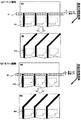
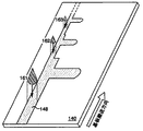
また、本発明に係る液滴吐出システムは、前記データに基づいて、前記薄膜を構成する材料を含む組成物を吐出するための第1及び第2のノズルの移動経路を設定する設定手段と、前記組成物を吐出する空間における雰囲気、該空間の温度、および該空間の湿度のパラメータが蓄積されたデータベースと、基板上に形成されたアライメントマーカーを検出するための撮像手段と、前記第1及び第2のノズルの移動経路を制御する制御手段と、前記データベースに基づいて前記組成物を吐出する空間における雰囲気、該空間の温度、および該空間の湿度を制御する手段とを有し、前記第2のノズルの移動経路は、前記第1のノズルの移動経路と交差するように設定され、ゲート電極と、半導体膜と、ソース電極およびドレイン電極を有する薄膜トランジスタを作製する液滴吐出システムであって、前記薄膜のパターンは、ゲート電極パターン、半導体膜パターン、ソース電極パターン、およびドレイン電極パターンを有し、前記ゲート電極の形成と、前記半導体膜をエッチングするためのマスクパターンの形成と、前記ソース電極および前記ドレイン電極の形成と、に用いられ、前記第2のノズルの移動経路は、前記第1のノズルの移動経路と直交するように設定され、前記第2の移動経路の組成物は、前記第1の移動経路との交差する部分で切断され、逆T字形状の薄膜を形成することを特徴とする。 Further, the droplet discharge system according to the present invention, based on the data, setting means for setting the movement path of the first and second nozzles for discharging the composition containing the material constituting the thin film, A database in which parameters of the atmosphere in the space for discharging the composition, the temperature of the space, and the humidity of the space are accumulated; imaging means for detecting an alignment marker formed on a substrate; Control means for controlling the movement path of the second nozzle, and means for controlling the atmosphere in the space for discharging the composition based on the database, the temperature of the space, and the humidity of the space, The movement path of the second nozzle is set so as to intersect the movement path of the first nozzle, and is a thin film having a gate electrode, a semiconductor film, a source electrode, and a drain electrode A droplet discharge system for manufacturing a transistor, wherein the thin film pattern includes a gate electrode pattern, a semiconductor film pattern, a source electrode pattern, and a drain electrode pattern. The formation of the gate electrode and the etching of the semiconductor film Used to form a mask pattern for forming the source electrode and the drain electrode, and the movement path of the second nozzle is set to be orthogonal to the movement path of the first nozzle, The composition of the second movement path is cut at a portion intersecting with the first movement path to form an inverted T-shaped thin film.
上記発明によれば、同一層(レイヤー)からなる交差する形状の薄膜を簡単に形成することができる。また、第1及び第2のノズルのうち、一方のノズルから前記組成物が連続的に吐出されるようにし、他方のノズルから前記組成物が断続的に吐出されるようにすることにより、線状部分と突出部分とからなる形状(⊥状、亠状)の薄膜を形成することができる。つまり、線状部分は、第1のノズルから組成物を連続的に吐出して形成し、突出部分は、前記第1のノズルと交差する方向(例えば、直交する方向)に第2のノズルを移動させ、組成物を断続的に吐出して形成することにより、最終的に、線状部分と突出部分とからなる形状の一の薄膜を形成することができる。例えば、アクティブマトリクス型表示装置に用いられるTFTのゲート配線及びゲート電極、あるいはソース信号線及びソース電極を同一レイヤーとして形成する際に、上記発明を適用することができる。 According to the said invention, the thin film of the shape which cross | intersects which consists of the same layer (layer) can be formed easily. In addition, the composition is continuously discharged from one of the first and second nozzles, and the composition is intermittently discharged from the other nozzle. It is possible to form a thin film having a shape (a bowl-like shape or a bowl-like shape) composed of a protruding portion and a protruding portion. That is, the linear portion is formed by continuously ejecting the composition from the first nozzle, and the protruding portion has the second nozzle in a direction crossing the first nozzle (for example, a direction orthogonal to the first nozzle). By moving and discharging the composition intermittently, a thin film having a shape composed of a linear portion and a protruding portion can be finally formed. For example, the present invention can be applied when forming a gate wiring and a gate electrode of a TFT used in an active matrix display device or a source signal line and a source electrode as the same layer.
なお、第1及び第2のノズルから吐出される組成物の種類は、基本的には同じものであるが、薄膜の機能を損なわない限り、異なる組成物を用いても構わない。例えば、上記ゲート配線部又はソース信号線部を、AlやCuを含む組成物を吐出することによって形成し、ゲート電極部又はソース電極部を、Agを含む組成物を吐出することによって形成することができる。他にもコストや抵抗率などを考慮して、適当な材料を選択することができる。 The types of compositions ejected from the first and second nozzles are basically the same, but different compositions may be used as long as the function of the thin film is not impaired. For example, the gate wiring portion or the source signal line portion is formed by discharging a composition containing Al or Cu, and the gate electrode portion or the source electrode portion is formed by discharging a composition containing Ag. Can do. In addition, an appropriate material can be selected in consideration of cost, resistivity, and the like.
また、上記発明では、複数のノズルを用いて線状部分と突出部分とからなる形状の薄膜を形成したが、固定されたノズルを用い、被吐出物である基板を少なくとも第1及び第2の経路に従って移動させることにより、同一層(レイヤー)からなる交差する形状の薄膜を簡単に形成することができる。また、前記基板が、第1及び第2の経路の一方を通過する際に、前記組成物が吐出されるノズルから前記組成物が連続的に吐出され、他方を通過する際に、前記ノズルから前記組成物が断続的に吐出されるように、基板の移動経路を制御することにより、上記線状部分と突出部分とからなる形状の薄膜を形成することができる。なお、吐出される組成物は、薄膜の機能を損なわない限り、基板の第1の移動経路と、第2の移動経路とで変更してもよい。 Further, in the above invention, a thin film having a linear portion and a protruding portion is formed using a plurality of nozzles, but at least the first and second substrates as discharge objects are formed using fixed nozzles. By moving according to the path, it is possible to easily form an intersecting thin film made of the same layer. Further, when the substrate passes through one of the first and second paths, the composition is continuously discharged from a nozzle from which the composition is discharged, and from the nozzle when it passes through the other. By controlling the movement path of the substrate so that the composition is intermittently discharged, a thin film having the shape of the linear portion and the protruding portion can be formed. Note that the composition to be discharged may be changed between the first movement path and the second movement path of the substrate as long as the function of the thin film is not impaired.
また、本発明に係る組成物吐出条件制御プログラムは、薄膜を構成する材料を含む組成物の吐出条件を制御するコンピュータを、前記コンピュータに入力された前記薄膜のパターンを示すデータから、前記組成物を吐出するためのノズルの移動経路、又は前記組成物が吐出される基板の移動経路を設定する設定手段として機能させるという特徴を有している。 Further, the composition discharge condition control program according to the present invention includes a computer for controlling discharge conditions of a composition including a material constituting a thin film, from the data indicating the pattern of the thin film input to the computer. It has a feature of functioning as a setting means for setting a movement path of a nozzle for discharging the liquid or a movement path of a substrate on which the composition is discharged.
上記発明によれば、液滴吐出システムを制御するコンピュータに前記組成物吐出条件制御プログラムが読み込まれることにより、該コンピュータに入力された、CAD等によって作成された薄膜パターンを示すデータに基づいて、前記薄膜を構成する材料を含む組成物を吐出するためのノズルの移動経路、又は該組成物が吐出される基板の移動経路を設定することができる。そして、ノズル又は基板を設定された移動経路に従って移動させ、前記ノズルの吐出口から前記組成物を吐出することにより、所望の位置に、所望の形状を有する薄膜や配線を形成することができる。 According to the above invention, by reading the composition discharge condition control program into a computer that controls the droplet discharge system, based on data indicating a thin film pattern created by CAD or the like input to the computer, It is possible to set a movement path of a nozzle for discharging a composition containing a material constituting the thin film, or a movement path of a substrate from which the composition is discharged. A thin film or wiring having a desired shape can be formed at a desired position by moving the nozzle or the substrate according to a set movement path and discharging the composition from the discharge port of the nozzle.
また、薄膜パターンを示すデータと共に、薄膜を構成する材料を含む組成物の種類を入力することにより、所望のノズル若しくは吐出口、又は該組成物を貯蔵するタンクを選択することもできる。 In addition, by inputting the data indicating the thin film pattern and the type of the composition including the material constituting the thin film, a desired nozzle or discharge port or a tank for storing the composition can be selected.
なお、本発明に係る組成物吐出条件制御プログラムは、前記設定手段によって設定されたノズル又は基板の移動速度、前記ノズルの吐出口と前記基板との距離、該吐出口から前記組成物を吐出する速度、前記組成物を吐出する空間における雰囲気、該空間の温度、該空間の湿度及び前記基板を加熱する温度のうち、少なくとも一を判断する判断手段を有することを特徴としている。 The composition discharge condition control program according to the present invention discharges the composition from the nozzle or substrate moving speed set by the setting means, the distance between the nozzle discharge port and the substrate, and the discharge port. It has a judging means for judging at least one of speed, atmosphere in a space for discharging the composition, temperature in the space, humidity in the space, and temperature for heating the substrate.
上記発明によれば、液滴吐出システムをより完全に制御することができ、良好な薄膜を高いスループットで作製することができる。 According to the above invention, the droplet discharge system can be more completely controlled, and a good thin film can be produced with high throughput.
なお、上記発明でいう薄膜とは、導電膜、絶縁膜、半導体膜、マスクパターン、有機化合物又は無機化合物を含む膜、カラーフィルタ、配向膜等、液滴吐出法によって形成することができるあらゆる膜を指す。 Note that the thin film as used in the above invention refers to any film that can be formed by a droplet discharge method, such as a conductive film, an insulating film, a semiconductor film, a mask pattern, a film containing an organic compound or an inorganic compound, a color filter, an alignment film, and the like. Point to.
例えば、導電膜としては、半導体素子におけるゲート電極、ソース電極、ドレイン電極、表示装置における画素電極、ELディスプレイのような発光装置における正孔注入電極(陽極)、電子注入電極(陰極)、あるいは、これらの電極に接続された信号線、走査線等の各種配線等が挙げられる。また、絶縁膜としては、半導体素子におけるゲート絶縁膜、半導体素子の上方に設けられる層間絶縁膜、平坦化膜、上記発光装置におけるバンク(土手、隔壁等とも呼ばれる。)等が挙げられる。また、半導体膜としては、半導体素子におけるチャネル領域や、不純物が添加されたソース、ドレイン領域等に用いられるシリコン膜、ゲルマニウム膜、シリコン・ゲルマニウム膜等が挙げられる。 For example, as a conductive film, a gate electrode, a source electrode, a drain electrode in a semiconductor element, a pixel electrode in a display device, a hole injection electrode (anode) in a light emitting device such as an EL display, an electron injection electrode (cathode), or Examples thereof include various wirings such as signal lines and scanning lines connected to these electrodes. Examples of the insulating film include a gate insulating film in a semiconductor element, an interlayer insulating film provided over the semiconductor element, a planarization film, and a bank (also referred to as a bank or a partition wall) in the light-emitting device. Examples of the semiconductor film include a silicon film, a germanium film, and a silicon / germanium film used for a channel region in a semiconductor element, a source / drain region to which an impurity is added, and the like.
また、マスクパターンとしては、レジストや、ポリイミド、アクリル、ポリイミド、ポリベンゾイミダゾールのような耐熱性高分子材料等が挙げられる。液滴吐出法によって形成されたマスクパターンは、前記導電膜、絶縁膜、半導体膜等を液滴吐出法によらず、CVD法やスパッタ法等の薄膜形成法によって形成した場合に、エッチングする際のマスクとして活用することができる。 Examples of the mask pattern include a resist, a heat resistant polymer material such as polyimide, acrylic, polyimide, and polybenzimidazole. The mask pattern formed by the droplet discharge method is used when the conductive film, the insulating film, the semiconductor film, or the like is etched when the thin film formation method such as the CVD method or the sputtering method is formed without using the droplet discharge method. Can be used as a mask.
また、有機化合物又は無機化合物を含む膜としては、上記発光装置における発光素子(代表的にはエレクトロルミネセンス(EL:Electro Luminescence)を利用した発光素子)を構成する、正孔注入層(ホール注入層)、正孔輸送層(ホール輸送層)、発光層、電子輸送層、電子注入層、ホールブロッキング層等が挙げられる。 In addition, as a film containing an organic compound or an inorganic compound, a hole injection layer (hole injection) that constitutes a light emitting element (typically, a light emitting element using electroluminescence (EL)) in the above light emitting device. Layer), hole transport layer (hole transport layer), light emitting layer, electron transport layer, electron injection layer, hole blocking layer, and the like.
薄膜や配線の形成に用いられる液滴吐出システムにおいて、本発明のごとく、薄膜パターンを示すデータを入力する入力手段と、前記データに基づいて、前記薄膜を構成する材料を含む組成物を吐出するためのノズルの移動経路を設定する設定手段と、基板上に形成されたアライメントマーカーを検出するための撮像手段と、前記ノズルの移動経路を制御する制御手段とを有する構成とすることにより、液滴吐出時におけるノズル又は基板の移動経路を的確に制御する必要がある。液滴吐出システムを制御するコンピュータに組成物吐出条件制御プログラムを読み込ませることにより、吐出する組成物やそのパターンに応じて、ノズル又は基板移動速度、組成物の吐出量・噴射距離・噴射速度、吐出環境の雰囲気・温度・湿度、基板加熱温度などの諸条件も的確に制御することができる。 In a droplet discharge system used for forming a thin film or wiring, as in the present invention, an input means for inputting data indicating a thin film pattern and a composition containing a material constituting the thin film are discharged based on the data. A configuration having a setting means for setting a movement path of a nozzle for the purpose, an imaging means for detecting an alignment marker formed on the substrate, and a control means for controlling the movement path of the nozzle. It is necessary to accurately control the movement path of the nozzle or the substrate during droplet discharge. By reading a composition discharge condition control program into a computer that controls the droplet discharge system, the nozzle or substrate moving speed, the discharge amount of the composition, the injection distance, the injection speed, Various conditions such as the atmosphere / temperature / humidity of the discharge environment and the substrate heating temperature can be controlled accurately.
これによって、所望の太さ、厚さ、形状を有する薄膜や配線を、短いタクトタイム、高スループットの下で、所望の箇所に精度良く作製することができ、ひいては、それらの薄膜や配線を用いて作製したTFTのような半導体素子、該半導体素子を用いて作製した液晶ディスプレイ(LCD)、有機ELディスプレイ(OELD)のような発光装置、LSI等の製造歩留まりを向上させることができる。特に、本発明を用いることにより、任意の場所に薄膜や配線のパターンを形成でき、形成するパターンの太さ、厚さ、形状も調整できるので、一辺が1〜2mを越える、例えば6畳分にも及ぶ大面積の半導体素子基板等も、低コストで歩留まり良く製造することができる。 As a result, a thin film or wiring having a desired thickness, thickness, and shape can be accurately produced at a desired location under a short tact time and a high throughput. The manufacturing yield of a semiconductor element such as a TFT manufactured in this way, a light emitting device such as a liquid crystal display (LCD) or an organic EL display (OELD) manufactured using the semiconductor element, LSI, or the like can be improved. In particular, by using the present invention, a thin film or wiring pattern can be formed at an arbitrary place, and the thickness, thickness, and shape of the pattern to be formed can be adjusted. A large-area semiconductor element substrate and the like can be manufactured at a low cost and with a high yield.
[実施の形態1]
本発明を用いた液滴吐出システムについて、図1、図4(A)を参照して説明する。
[Embodiment 1]
A droplet discharge system using the present invention will be described with reference to FIGS. 1 and 4A.
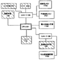
まず、CAD、CAM、CAE等の回路設計ツール100によって、回路設計が行われ、所望の薄膜及びアライメントマーカーの配置箇所を決定する。
First, circuit design is performed by a
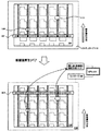
次に、設計された薄膜及びアライメントマーカーの配置箇所を含む薄膜パターンのデータ101は、記録媒体又はLAN(Local Area Network)等の情報網を介して、液滴吐出装置を制御するコンピュータ102に入力される。そして、薄膜パターンのデータ101に基づいて、液滴吐出手段103が有するノズル(筒状の、先の細い穴から液体や気体を噴出させる装置)のうち、該薄膜を構成する材料を含む組成物を貯蔵し、又は該組成物を貯蔵するタンクと接続されている最適な吐出口径を有するノズルが決定され、続いて、液滴吐出手段103の走査経路(移動経路)が決定される。なお、予め最適なノズルが決まっている場合いは、該ノズルの移動経路のみを設定すればよい。
Next, the thin
次に、該薄膜が形成される基板104上にフォトリソグラフィー技術やレーザー光を用いて、アライメントマーカー117を形成する。そして、アライメントマーカーが形成された基板を液滴吐出装置内のステージ116に設置し、該装置に具備された撮像手段105によりアライメントマーカーの位置を検出し、画像処理装置106を介して、コンピュータ102に位置情報107として入力される。コンピュータ102では、CAD等により設計された薄膜パターンのデータ101と、撮像手段105によって得られるアライメントマーカーの位置情報107とを照らし合わせて、基板104と液滴吐出手段103との位置合わせを行う。
Next, the alignment marker 117 is formed on the
その後、コントローラ108によって制御された液滴吐出手段103が、決定された走査経路に従って、組成物118を吐出することにより、所望の薄膜パターン109が形成される。なお、組成物の吐出量は、吐出口の径を選択することにより、適宜調整することができるが、吐出口の移動速度、吐出口と基板との間隔、組成物の吐出速度、吐出空間の雰囲気、該空間の温度、湿度等のあらゆる条件によって微妙に異なってくるため、これらの条件も制御できるようにすることが望ましい。これらは、予め実験、評価によって最適な条件を求めておき、組成物の材料毎にデータベース化しておくのがよい。
Thereafter, the droplet discharge means 103 controlled by the
ここで、薄膜パターンデータとしては、例えば、液晶表示装置、EL表示装置等に用いられるアクティブマトリクス型TFT基板の回路図等が挙げられる。図1中の円内の回路図は、このようなアクティブマトリクス型TFT基板に用いられる導電膜を模式的に示したものである。121は所謂ゲート配線、122はソース信号線(2nd配線)、123は画素電極又は正孔注入電極若しくは電子注入電極を指す。また、120は基板、124はアライメントマーカーを示している。当然、薄膜パターン109は、薄膜パターン情報におけるゲート配線121に対応するものである。
Here, as the thin film pattern data, for example, a circuit diagram of an active matrix TFT substrate used in a liquid crystal display device, an EL display device or the like can be cited. A circuit diagram in a circle in FIG. 1 schematically shows a conductive film used for such an active matrix TFT substrate. 121 is a so-called gate wiring, 122 is a source signal line (2nd wiring), and 123 is a pixel electrode, a hole injection electrode, or an electron injection electrode. Reference numeral 120 denotes a substrate, and 124 denotes an alignment marker. Naturally, the
また、液滴吐出手段103は、ここでは、ノズル110、111、112が一体化された構成となっているが、これに限定されるものではない。また、各ノズルは、それぞれ複数の吐出口113、114、115を有している。上記薄膜パターン109は、ノズル110のうち、所定の吐出口113を選択することによって形成されたものである。
In addition, the droplet discharge means 103 has a configuration in which the
なお、液滴吐出手段103は、あらゆる線幅の薄膜パターンの作製に対応できるように、また、タクトタイムを向上させるため、吐出口径、吐出量、又はノズルピッチの異なる複数のノズルを備えておくのが望ましい。また、吐出口の間隔はできる限り狭い方が望ましい。また、一辺が1m以上から6畳程度の大面積の基板に対して、スループットの高い吐出を行うために、1m以上の長さを有するノズルを備えておくことが望ましい。また、伸縮機能を備え、吐出口の間隔を自由に制御することができるようにしてもよい。また、高解像度、即ち、滑らかなパターンを描画するために、ノズル又はヘッドが斜めに傾くようにしておくのが望ましい。これによって、矩形状など、大面積の描画が可能となる。 The droplet discharge means 103 is provided with a plurality of nozzles having different discharge port diameters, discharge amounts, or nozzle pitches in order to cope with the production of thin film patterns having any line width and to improve the tact time. Is desirable. Further, it is desirable that the interval between the discharge ports be as narrow as possible. In addition, it is desirable to provide a nozzle having a length of 1 m or more in order to perform high-throughput discharge on a large area substrate having a side of 1 m or more to 6 tatami mats. Further, an expansion / contraction function may be provided so that the interval between the discharge ports can be freely controlled. In order to draw a high resolution, that is, a smooth pattern, it is desirable that the nozzle or the head be inclined obliquely. As a result, a large area such as a rectangular shape can be drawn.
また、ヘッドのノズルピッチを変えたものを一つのヘッドに平行に備え付けてもよい。この場合、吐出口径は同じでもよいし、異ならせてもよい。 Further, a head having a different nozzle pitch may be provided in parallel with one head. In this case, the discharge port diameter may be the same or different.
また、上記のように、複数のノズルを用いた液滴吐出装置となる場合には、使用していないノズルを収納するための、待機場所を設けておく必要がある。この待機場所には、またガス供給手段とシャワーヘッドを設けることにより、組成物の溶媒と同じ気体の雰囲気下に置換することができるため、乾燥をある程度防止することができる。さらに、清浄な空気を供給し、作業領域の埃を低減するクリーンユニット等を備え付けてもよい。 Further, as described above, when a droplet discharging device using a plurality of nozzles, for accommodating the nozzles not in use, it is necessary to provide a waiting position. In this standby place, by providing a gas supply means and a shower head, the atmosphere can be replaced with the same gas atmosphere as the solvent of the composition, so that drying can be prevented to some extent. Furthermore, you may equip with the clean unit etc. which supply clean air and reduce the dust of a working area.
ただし、ノズルの仕様上、吐出口の間隔が狭くできないときには、ノズルピッチが表示装置における画素の整数倍となるように設計するとよい。これによって、図16のように、ノズルをずらして組成物を吐出することができる。 However, when the interval between the discharge ports cannot be reduced due to the specification of the nozzle, the nozzle pitch may be designed to be an integer multiple of the pixels in the display device. As a result, as shown in FIG. 16, the composition can be discharged by shifting the nozzle.
また、撮像手段105としては、CCD(電荷結合素子)のような光の強弱を電気信号に変換する半導体素子を用いたカメラを用いればよい。 As the imaging means 105, a camera using a semiconductor element that converts light intensity into an electric signal, such as a CCD (charge coupled device), may be used.
上述した方法は、基板104を載せたステージ116を固定し、液滴吐出手段103を決定された経路に従って走査させることによって、薄膜パターン109を形成するものである。それに対して、液滴吐出手段103を固定し、薄膜パターンのデータ101に基づいて決定された経路に従って、ステージ116をXYθ方向に搬送させることによって、薄膜パターン109を形成してもよい。この際、液滴吐出手段103が複数のノズルを有している場合には、該薄膜を構成する材料を含む組成物を貯蔵し、又は該組成物を貯蔵するタンクと接続されている最適な吐出口径を有するノズルを決定する必要がある。
In the method described above, the
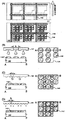
また、上述した方法は、ノズル110の所定の一つの吐出口のみを用いて薄膜パターン109を吐出形成するものであるが、形成する薄膜の線幅や膜厚に応じて、図12〜15に示すように、複数の吐出口を用いて組成物を吐出してもよい。
In the above-described method, the
また、複数のノズルを用い、冗長機能を持たせてもよい。例えば、最初にノズル112(又は111)から組成物が吐出されるが、ノズル110からも、同一の組成物が吐出されるよう吐出条件を制御することにより、前方のノズル112において吐出口詰まり等の支障を来しても、後方のノズル110から組成物を吐出することができるため、少なくとも配線の断線等を防止することが可能となる。
A plurality of nozzles may be used to provide a redundant function. For example, the composition is first ejected from the nozzle 112 (or 111), but by controlling the ejection conditions so that the same composition is also ejected from the
また、吐出口径の異なる複数のノズルから組成物を吐出するように吐出条件を制御することにより、図12、13に示すように、平坦な薄膜を、より短縮されたタクトタイムで形成することができる。この方法は、特にLCDにおける画素電極や、ELディスプレイにおける正孔注入電極又は電子注入電極(図1の123に相当)のように、組成物の吐出面積が大きく、かつ平坦性が要求されるような薄膜の形成に特に適している。 Further, by controlling the discharge condition so as to discharge a composition different from the plurality of nozzles of the discharge aperture, sea urchin by it is shown in FIGS. 12 and 13, a flat thin film, to form a more shortened tact time Can do. This method requires a large discharge area of the composition and flatness, particularly like a pixel electrode in an LCD, a hole injection electrode or an electron injection electrode (corresponding to 123 in FIG. 1) in an EL display. It is particularly suitable for forming a thin film.
さらに、吐出口径の異なる複数のノズルから組成物を吐出するように吐出条件を制御することにより、図14のように、配線の線幅が異なるパターンを一度に形成することができる。 Furthermore, by controlling the discharge conditions so that the composition is discharged from a plurality of nozzles having different discharge port diameters, patterns having different line widths of wiring can be formed at a time as shown in FIG.
さらに、吐出口径の異なる複数のノズルから組成物を吐出するように吐出条件を制御することにより、図15のように、絶縁膜12の一部に設けられたアスペクト比が高い開孔部に、組成物を充填させることができる。この方法によれば、ボイド(絶縁膜12と配線の間に生じる虫食い状の孔)が生じることなく、平坦化された配線を形成することができる。
Furthermore, by controlling the discharge conditions so as to discharge the composition from a plurality of nozzles having different discharge port diameters, as shown in FIG. 15, in the opening portion having a high aspect ratio provided in a part of the insulating
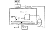
図2は、上述した液滴吐出システムを有する液滴吐出装置の側面図を示したものである。該液滴吐出装置の構成要素としては、複数のノズルが一軸方向に配列されたヘッドを具備する液滴吐出手段103、該液滴吐出手段103を制御するコントローラ108及びCPU201、基板104を固定しXYθ方向に可動するステージ116等が挙げられる。このステージ116は、基板104を真空チャック等の手法で固定する機能も有する。そして、液滴吐出手段103が有する各ノズルの吐出口から基板104の方向に組成物が吐出され、パターンが形成される。
FIG. 2 is a side view of a droplet discharge apparatus having the above-described droplet discharge system. As constituent elements of the droplet discharge device, a
ステージ116と液滴吐出手段103は、コントローラ203を介してCPU201により制御される。また、CCDカメラなどの撮像手段105もCPU201により制御される。撮像手段105は、基板104上に形成されたアライメントマーカーを検出するものであり、CPU201で画像処理を経た後、モニター202によってそれらの位置情報を確認することができる。また、液滴吐出手段103は、インクボトル200と接続され、液滴吐出手段103のノズル及びその吐出口に組成物が供給される。
The
なお、パターンの作製に際しては、液滴吐出手段103を移動してもよいし、液滴吐出手段103を固定してステージ116を移動させてもよい。但し、液滴吐出手段103を移動させる場合には、ノズル移動時の加速度や、液滴吐出手段103に具備されたノズルと被処理物との距離、その環境を考慮して行う必要がある。
In producing the pattern, the droplet discharge means 103 may be moved, or the
また、組成物を吐出する際の始点、終点又は方向転換点において、液だまり(バルジ)の生成を防止するため、ノズルから組成物が吐出されるまでのいわば助走区間を設け、基板又はノズルの加速度が一定になったときに組成物が吐出できるよう、移動距離を計算するプログラムを制御するコンピュータに組み込んでおくことが望ましい。 In addition, in order to prevent the formation of a puddle (bulge) at the start point, end point, or turning point when the composition is discharged, a so-called run-up section is provided until the composition is discharged from the nozzle. It is desirable to incorporate it into a computer that controls a program for calculating the movement distance so that the composition can be discharged when the acceleration becomes constant.
その他、図示しないが、付随する構成要素として、吐出した組成物の着弾精度を向上させるために、ノズルのヘッド(吐出口)113〜115が上下に動く移動機構とその制御手段等を設けてもよい。そうすると、吐出する組成物の特性に応じて、吐出口と基板104の距離を変えることができる。またガス供給手段とシャワーヘッドを設けることにより、組成物の溶媒と同じ気体の雰囲気下に置換することができるため、乾燥をある程度防止することができる。さらに、清浄な空気を供給し、作業領域の埃を低減するクリーンユニット等を設けてもよい。また、図示しないが、基板を加熱する手段、加えて温度、圧力等、種々の物性値を測定する手段を、必要に応じて設置しても良く、これら手段も、筐体の外部に設置した制御手段によって一括制御することが可能である。さらに制御手段をLANケーブル、無線LAN、光ファイバ等で生産管理システム等に接続すれば、工程を外部から一律管理することが可能となり、生産性を向上させることに繋がる。なお、着弾した組成物の乾燥を早め、また組成物の溶媒成分を除去するために、真空排気を行って、減圧下で動作させてもよい。
In addition, although not shown in the drawings, as an accompanying component, in order to improve the landing accuracy of the discharged composition, a moving mechanism in which the nozzle heads (discharge ports) 113 to 115 move up and down, its control means, and the like may be provided. Good. Then, the distance between the ejection port and the
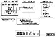
図3は、本発明の液滴吐出システムの機構を模式的に示した図である。まず、CAD等の回路設計ツールによって作成された薄膜パターンを示すデータ及び組成物の種類等の情報を端末300からコンピュータ102に入力する。そして、入力された該薄膜パターンデータに基づいて、設定手段301によって、該薄膜を構成する材料を含む組成物を吐出するノズルの移動経路、又は該組成物が吐出される基板を支える基板搬送機構の移動経路が設定される。また、基板に形成されたアライメントマーカーを、CCDカメラ等の撮像手段105によって検出しておき、撮像手段によって得られた位置情報と、前記薄膜パターンデータを照らし合わせることによって、基板とノズルとの位置合わせを行うことができる。そして、制御手段304によって吐出機構302又は基板搬送機構303を設定された移動経路に従って移動させ、前記ノズルの吐出口から前記組成物を吐出することにより、所望の位置に、所望の形状を有する薄膜を形成することができる。
FIG. 3 is a diagram schematically showing the mechanism of the droplet discharge system of the present invention. First, data indicating a thin film pattern created by a circuit design tool such as CAD and information such as the type of composition are input from the terminal 300 to the
[参考形態1]
実施の形態1では、基板に形成されたアライメントマーカーを用いて、基板とノズルの位置合わせを行う場合について説明したが、本参考形態では、基板上に既に形成された第1の薄膜パターンを撮像手段105によって検出し、その位置情報と、CAD等によって作成された第2の薄膜パターンのデータ101とを照らし合わせることにより、基板と第2の薄膜を構成する材料を含む組成物を吐出するためのノズルとの位置合わせを行う場合について、図4(B)を参照して説明する。
[ Reference form 1 ]
In the first embodiment, the case where alignment of the substrate and the nozzle is performed using the alignment marker formed on the substrate has been described, but in this reference embodiment, the first thin film pattern already formed on the substrate is imaged. In order to discharge the composition containing the material constituting the substrate and the second thin film by comparing the position information detected by the
まず、基板上に第1の薄膜パターンを形成する。第1の薄膜パターンは、実施の形態1と同様のシステム及び手法により作製してもよい。 First, a first thin film pattern is formed on a substrate. The first thin film pattern may be produced by the same system and method as in the first embodiment.
次に、入力手段によって、第2の薄膜パターンのデータをコンピュータ102に入力する。そして、入力された第2の薄膜パターンのデータに基づいて、設定手段301によって、該薄膜を構成する材料を含む組成物を吐出するノズルの移動経路、又は該組成物が吐出される基板を支える基板搬送機構の移動経路が設定される。
Next, the data of the second thin film pattern is input to the
次に、撮像手段105を用いて、第1の薄膜パターンを検出し、その位置情報と、CAD等によって作成された第2の薄膜パターンのデータとを照らし合わせることにより、基板と第2の薄膜を構成する材料を含む組成物を吐出するためのノズルとの位置合わせ(アライメント)を行う。
Next, the
次に、設定された移動経路に従って、前記ノズル又は基板搬送機構を移動させ、前記ノズルの吐出口から前記組成物を吐出することにより、所望の位置に、所望の形状を有する第2の薄膜パターンを即座に形成することができる。 Next, the second thin film pattern having a desired shape is formed at a desired position by moving the nozzle or the substrate transport mechanism according to the set movement path and discharging the composition from the discharge port of the nozzle. Can be formed instantly.
同様に、第3の薄膜パターンデータを入力し、ノズル又は基板の移動経路を設定し、一方で、第1又は第2の薄膜パターンを撮像手段105によって検出し、基板とノズルとの位置合わせを行い、設定された移動経路に従って、前記ノズル又は基板搬送機構を移動させ、前記ノズルの吐出口から組成物を吐出することにより、所望の位置に、所望の形状を有する第3の薄膜パターンを即座に形成することもできる。 Similarly, the third thin film pattern data is input and the movement path of the nozzle or the substrate is set. On the other hand, the first or second thin film pattern is detected by the imaging means 105, and the alignment between the substrate and the nozzle is performed. The third thin film pattern having a desired shape is immediately formed at a desired position by moving the nozzle or the substrate transport mechanism according to the set movement path and discharging the composition from the discharge port of the nozzle. It can also be formed.
なお、本参考形態は、上記実施の形態又は下記実施例、参考例と自由に組み合わせることができる。 In addition, this reference form can be freely combined with the said embodiment or the following Example and reference example .
[実施の形態2]
本実施の形態では、実施の形態1、参考形態1で述べたノズル又は基板搬送機構の移動経路を設定する手段に加え、他の吐出条件を設定する手段を有する液滴吐出システムについて、図1、図5を参照して説明する。
[Embodiment 2 ]
In the present embodiment, a droplet discharge system having means for setting other discharge conditions in addition to the means for setting the movement path of the nozzle or substrate transfer mechanism described in
本実施の形態で説明する液滴吐出システムは、吐出する組成物の特性に応じて、最適な吐出条件を蓄積したデータベース119(図1)を利用して、ノズル又は基板の移動速度、組成物の吐出量、ノズルヘッドと基板との距離、吐出口から組成物を吐出する速度、組成物を吐出する空間における雰囲気、該空間の温度、該空間の湿度及び基板を加熱する温度等の組成物吐出条件を自動的に制御することができる機能を有することを特徴としている。 The droplet discharge system described in this embodiment uses a database 119 (FIG. 1) in which optimal discharge conditions are accumulated according to the characteristics of the composition to be discharged, and the nozzle or substrate moving speed, composition Composition such as the discharge amount of the nozzle, the distance between the nozzle head and the substrate, the speed at which the composition is discharged from the discharge port, the atmosphere in the space in which the composition is discharged, the temperature in the space, the humidity in the space, and the temperature in which the substrate is heated It is characterized by having a function capable of automatically controlling discharge conditions.
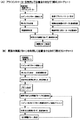
図5は、該液滴吐出システムによって薄膜を形成する際のフローチャートである。まず、実施の形態1、2と同様の設定手段によって、最適なノズル、及び、基板又はノズルの移動経路を決定する。 FIG. 5 is a flowchart for forming a thin film by the droplet discharge system. First, the optimum nozzle and the substrate or nozzle movement path are determined by the same setting means as in the first and second embodiments.
次に、吐出する組成物の特性に応じて、ノズル又は基板の移動速度、組成物の吐出量、ノズルヘッドと基板との距離、吐出口から組成物を吐出する速度、組成物を吐出する空間における雰囲気、該空間の温度、該空間の湿度及び基板を加熱する温度を設定する。これらの条件は、理論的又は実験的、経験的に得られたパラメータが多数蓄積されたデータベースを用い、設計された薄膜パターンデータ101と、組成物の種類、膜厚等の情報と照らし合わせることにより、最適なパラメータを判断するための判断手段によって決定される。
Next, depending on the characteristics of the composition to be discharged, the moving speed of the nozzle or the substrate, the discharge amount of the composition, the distance between the nozzle head and the substrate, the speed at which the composition is discharged from the discharge port, the space for discharging the composition Atmosphere, temperature of the space, humidity of the space, and temperature for heating the substrate are set. These conditions should be compared with the designed thin
そして、決定された吐出条件に従って、液滴吐出装置の各機構がコントローラ108によって制御される。例えば、ノズルヘッドと基板との距離は、ノズルのヘッド(吐出口)113〜115が上下に動く移動機構を制御することによって変えることができる。
Then, each mechanism of the droplet discharge device is controlled by the
また、液滴吐出手段103が有するヘッドとして、振動板、下部電極、ピエゾ、上部電極からなるピエゾ素子(圧電素子)を用いた圧電方式(ピエゾ方式)を採用した場合、該方式は、上部電極と下部電極に電位差を設けることにより、電極間に挟まれたピエゾが撓み、液滴が吐出される仕組みになっているため、これらの電極に印加する電圧を変えることによって、組成物の吐出量、又は組成物の吐出速度を制御することができる。なお、溶液の材料によっては、前記圧電素子を発熱体に置換した構造を有し、該発熱体を発熱させ気泡を生じさせ溶液を押し出す、所謂バブルジェット方式を用いてもよい。この場合、該発熱体の発熱温度等を変えることによって、組成物の吐出量、又は組成物の吐出速度を制御することができる。 Further, when a piezoelectric method (piezo method) using a piezoelectric element (piezoelectric element) composed of a diaphragm, a lower electrode, a piezo, and an upper electrode is employed as the head of the droplet discharge means 103, the method uses the upper electrode. and by providing a potential difference lower electrode, deflection piezo sandwiched between electrodes, because it is a mechanism in which the droplets are ejected by changing the voltage to be marked addition to these electrodes, the discharge of the composition The amount or the discharge speed of the composition can be controlled. Depending on the material of the solution, a so-called bubble jet method may be used in which the piezoelectric element is replaced with a heating element, and the heating element generates heat to generate bubbles to push out the solution. In this case, the discharge amount of the composition or the discharge speed of the composition can be controlled by changing the heat generation temperature of the heating element.
また、吐出空間の雰囲気制御を行う場合、N2、O2や有機ガス等の中から、吐出する組成物の特性に応じて選択すればよい。また、吐出空間の温度や、基板加熱温度も、組成物の特性に応じて、制御することができる。また、吐出形成後の処理に併せて、これらの温度を調整してもよい。例えば、導電材料を含む組成物を吐出した後、乾燥、焼成工程をへて導電膜が形成されるが、この乾燥、焼成工程に併せて、温度を調整することができる。一例として、Agを含む組成物(Agナノペースト)を吐出形成した後、N2+O2雰囲気(O2組成比は10〜30%が望ましい。)で200〜250℃に焼成することにより、平坦かつ低抵抗の導電膜を形成することができる。 Further, when controlling the atmosphere of the discharge space, it may be selected from N 2 , O 2 , organic gas, etc. according to the characteristics of the composition to be discharged. Also, the temperature of the discharge space and the substrate heating temperature can be controlled according to the characteristics of the composition. Further, these temperatures may be adjusted in accordance with the process after the discharge formation. For example, after discharging a composition containing a conductive material, a conductive film is formed through drying and baking processes. The temperature can be adjusted in accordance with the drying and baking processes. As an example, a composition containing Ag (Ag nanopaste) is discharged and formed, and then fired at 200 to 250 ° C. in an N 2 + O 2 atmosphere (O 2 composition ratio is preferably 10 to 30%), thereby flattening. In addition, a low resistance conductive film can be formed.
以上のように、前記データベースと判断手段によって吐出条件を制御することにより、所望の薄膜を高スループットで形成することができる。 As described above, a desired thin film can be formed at a high throughput by controlling the discharge conditions by the database and the judging means.
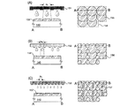
本実施例では、図6、7を参照して、本発明に係る液滴吐出システムを用いて、アクティブマトリクス基板のTFTにおけるゲート配線及びゲート電極を形成する方法について説明する。 In this embodiment, a method for forming a gate wiring and a gate electrode in a TFT of an active matrix substrate using a droplet discharge system according to the present invention will be described with reference to FIGS.
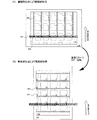
まず、ゲート配線部をノズル601から導電材料を含む組成物を吐出形成することによって形成する。ゲート配線部のパターンをコンピュータに入力することにより、ノズル601及び組成物が吐出される吐出口が選択され、基板の移動経路が設定手段を介して決定される。そして、該移動経路に従って基板が搬送され、選択された吐出口(図中黒色で示した部分)から組成物が連続的に吐出されることにより、ゲート配線603が形成される。なお、組成物は、断続的に吐出してもよいが、この場合には、導電膜の輪郭を滑らかにするため、図8、9に示したように、基板上に吐出された組成物の径の略半分のピッチ(以下、単に「半ドットピッチ」という。)で行うのが望ましい。
First, the gate wiring portion is formed by discharging and forming a composition containing a conductive material from the
前記導電材料としては、Ag、Au、Cu、Ni、Pt、Pd、Ir、Rh、W、Al、Ta、Mo、Cd、Zn、Fe、Ti、Si、Ge、Zr、Ba、ITO、ITSO、有機インジウム、有機スズ、酸化亜鉛(ZnO)のうち、少なくとも一種を含むものを用いることができる。ここでは、Agを含むナノペーストと呼ばれる組成物を用いた。このナノペーストは、Agを有機溶剤に分散又は溶解させたものであるが、他にも分散剤や、バインダーと呼ばれる熱硬化性樹脂が含まれている。特にバインダーに関しては、焼成時にクラックや不均一な焼きムラが発生するのを防止する働きを持つ。そして、乾燥又は焼成工程により、有機溶剤の蒸発、分散剤の分解除去及びバインダーによる硬化収縮が同時に進行することにより、ナノ粒子同士が融合し、ナノペーストが硬化する。この際、ナノ粒子は、数十〜百数十nmまで成長し、近接する成長粒子同士で融着、及び互いに連鎖することにより、金属連鎖体を形成する。一方、残った有機成分の殆ど(約80〜90%)は、金属連鎖体の外部に押し出され、結果として、金属連鎖体を含む導電膜と、その外側を覆う有機成分からなる膜が形成される。 Examples of the conductive material include Ag, Au, Cu, Ni, Pt, Pd, Ir, Rh, W, Al, Ta, Mo, Cd, Zn, Fe, Ti, Si, Ge, Zr, Ba, ITO, ITSO, Among organic indium, organic tin, and zinc oxide (ZnO), those containing at least one kind can be used. Here, a composition called a nanopaste containing Ag was used. This nanopaste is obtained by dispersing or dissolving Ag in an organic solvent, but also contains a dispersant and a thermosetting resin called a binder. In particular, the binder has a function of preventing occurrence of cracks and uneven baking during firing. Then, by the drying or firing step, evaporation of the organic solvent, decomposition removal of the dispersant, and curing shrinkage by the binder proceed simultaneously, whereby the nanoparticles are fused and the nanopaste is cured. At this time, the nanoparticles grow to several tens to one hundred and several tens of nanometers, and are fused together and chained together to form a metal chain. On the other hand, most of the remaining organic components (about 80 to 90%) are pushed out of the metal chain, and as a result, a conductive film containing the metal chain and a film made of organic components covering the outside are formed. The
ゲート配線603が形成された後、基板104を載せたステージ116を時計回りに90°回転させ、引き続き、ゲート電極部を、ノズル601から導電材料を含む組成物を吐出形成することによって形成する。まず、ゲート電極部のパターンをコンピュータに入力することにより、ノズル601及び組成物が吐出される吐出口が選択され、基板の移動経路が設定手段を介して決定される。そして、該移動経路に従って基板が搬送され、選択された吐出口(図中黒色で示した部分)から組成物が断続的に吐出されることにより、ゲート電極604が形成される。
After the
前記導電材料としては、ゲート配線603と同様にAgを用いたが、上記に掲げた材料の中から他の材料を選択してもよい。また、ノズル601の吐出量を制御することにより、異なる線幅のゲート配線603、ゲート電極604を形成することができる。
As the conductive material, Ag is used similarly to the
なお、ゲート配線603、ゲート電極604は、組成物を吐出形成した後、乾燥、焼成工程を経て、形成されるが、該乾燥、焼成工程は、吐出形成がすべて終わった後に行ってもよいし、ゲート配線603、ゲート電極604毎に行ってもよい。焼成工程は、Agを含む組成物(Agナノペースト)を用いた場合、平坦かつ低抵抗の導電膜を形成するために、N2+O2雰囲気(O2組成比は10〜30%が望ましい。)で200〜250℃に焼成するのがよい。
Note that the
また、ここでは、ゲート配線603、ゲート電極604を構成する導電材料としては同じものと用いたが、導電膜としての機能を損なわない限り、異なる導電材料を用いてもよい。例えば、ゲート配線603としてAl、Cuを用い、ゲート電極604としてAgを用いる、あるいはその逆とすることもできる。導電材料は、コスト面や抵抗値を考慮して、適宜選択することができる。
Here, the same conductive material is used for forming the
また、図6(A)、(B)の工程を複数回繰り返すことにより、多層構造のゲート配線603、ゲート電極604を形成することもできる。この場合にも、異なる材料を用いて、多層構造を構成することができる。
6A and 6B can be repeated a plurality of times to form the
また、本実施例においては、ノズル601は静止状態を保っていたが、XYθ方向に可動とさせてもよい。これによって、ノズルに冗長機能を持たせることもでき、ゲート配線603、ゲート電極604の断線部が形成されるのを防止することができる。
In the present embodiment, the
また、ゲート配線603、ゲート電極604は、図7に示すように、基板104を固定した状態において、複数のノズルによって形成してもよい。これらのノズルは、異なるノズルピッチ、吐出口径を有するものとしてもよい。ゲート配線603、ゲート電極604を構成する材料は、上述したものを用いることができる。なお、ノズルとしては、回転機構を有する一のノズルを用いて形成してもよく、ゲート配線603、ゲート電極604で、吐出量を異ならせてもよい。
Further, the
なお、本実施例に用いる液滴吐出システムとしては、上記実施の形態に示されたものを用いればよい。また、本実施例は、上記実施の形態又は他の実施例と自由に組み合わせることができる。また、本実施例に示す方法は、アクティブマトリクス基板のTFTにおけるゲート電極等の導電膜に限らず、他の液滴吐出法で形成しうるあらゆる膜の形成に適用することができる。 Note that the droplet discharge system used in this embodiment may be the one shown in the above embodiment. This embodiment can be freely combined with the above embodiment mode or other embodiments. The method shown in this embodiment is not limited to the conductive film such as the gate electrode in the TFT of the active matrix substrate, and can be applied to the formation of any film that can be formed by other droplet discharge methods.
本実施例では、図8、9を参照して、本発明に係る液滴吐出システムを用いて配線を形成する方法について説明する。 In this embodiment, a method for forming a wiring by using the droplet discharge system according to the present invention will be described with reference to FIGS.
基板上に、組成物を断続的に吐出する場合において、図8(A)、図9(A)のように、略1ドット(基板上に吐出された組成物の径)の間隔で吐出した場合、配線の形状は、著しい凹凸を有する形状となる。しかし、図8(B)、図9(B)のように、半ドットピッチで吐出した場合、配線の形状は、略1ドットピッチの場合に比べて、非常に滑らかな形状となる。 In the case of intermittently discharging the composition onto the substrate, it was discharged at an interval of approximately 1 dot (the diameter of the composition discharged onto the substrate) as shown in FIGS. 8A and 9A. In this case, the shape of the wiring is a shape having significant unevenness. However, as shown in FIGS. 8B and 9B, when ejection is performed at a half-dot pitch, the shape of the wiring is very smooth compared to the case of approximately one-dot pitch.
なお、図8は、ノズルの移動経路を、上→右→上→左→・・・→上→右→上→右→・・・といった要領で形成した、所謂冗長機能を有するものであり、図9は、基板の移動経路を、下→下→・・・→右下→右下→・・・といった要領で形成したものであるが、上記方法は、いずれの場合にも採用することができる。また、移動する部分をノズルと基板とで入れ替えても差し支えない。なお、上記方法は、組成物を連続的に吐出する場合にも応用することができる。 FIG. 8 has a so-called redundant function in which the nozzle movement path is formed in the manner of upper → right → upper → left → ・ ・ ・ → upper → right → upper → right → ... In FIG. 9, the substrate movement path is formed in the manner of lower → lower →... → lower right → lower right →..., But the above method can be adopted in any case. it can. Further, the moving part may be replaced with the nozzle and the substrate. In addition, the said method is applicable also when discharging a composition continuously.
また、さらに、前記組成物に含まれる導電材料とは異なる導電材料を含む組成物を吐出することにより、多層配線としてもよい。また、鋸刃の形状、又は凹凸状の配線とすることにより、アクティブマトリクス基板の周辺に設けられる保護回路を作成することもできる。この保護回路は、その特殊な形状を利用してTFT工程における配線への過剰な帯電を防ぐ、即ち、TFTの絶縁破壊を防止する機能を有し、放電パターンなどとも呼ばれる。 Furthermore, a multilayer wiring may be formed by discharging a composition containing a conductive material different from the conductive material contained in the composition. In addition, a protection circuit provided in the periphery of the active matrix substrate can be created by using a saw-blade shape or an uneven wiring. This protection circuit has a function of preventing excessive charging of the wiring in the TFT process by utilizing its special shape, that is, preventing a dielectric breakdown of the TFT, and is also called a discharge pattern or the like.
なお、本実施例に用いる液滴吐出システムとしては、上記実施の形態に示されたものを用いればよい。また、本実施例は、上記実施の形態又は他の実施例と自由に組み合わせることができる。また、本実施例に示す方法は、配線等の導電膜に限らず、他の液滴吐出法で形成しうるあらゆる膜の形成に適用することができる。 Note that the droplet discharge system used in this embodiment may be the one shown in the above embodiment. This embodiment can be freely combined with the above embodiment mode or other embodiments. Further, the method shown in this embodiment is not limited to the conductive film such as a wiring, and can be applied to the formation of any film that can be formed by other droplet discharge methods.
本実施例では、図10を参照して、本発明に係る液滴吐出システムを用いて、アクティブマトリクス基板のTFTにおける配線を形成する方法について説明する。 In this embodiment, a method for forming a wiring in a TFT of an active matrix substrate using the droplet discharge system according to the present invention will be described with reference to FIG.
まず、異なる吐出口径を有する少なくとも2つのノズル1001、1002を用意し、大きい吐出口径を有するノズル1001で、組成物1004を吐出形成する。次に、ノズル1001を半ドット分シフトさせ、組成物1005を吐出形成する。ここで、ノズル1001を半ドット分シフトさせることにより、滑らかな配線を形成することができる。
First, at least two
しかし、さらに滑らか且つ平坦な配線を形成する場合には、小さい吐出口径を有するノズル1002を用いて、組成物1004、1005の凹凸部を埋める要領で、組成物1006、1007を吐出すればよい。
However, when forming a smoother and flatter wiring, the
また、さらに、前記組成物に含まれる導電材料とは異なる導電材料を含む組成物を吐出することにより、多層配線としてもよい。 Furthermore, a multilayer wiring may be formed by discharging a composition containing a conductive material different from the conductive material contained in the composition.
また、前後に配置された複数のノズルを用いて、組成物を形成することにより、冗長機能を持たせることもできる。 Moreover, a redundant function can also be given by forming a composition using the some nozzle arrange | positioned forward and backward.
なお、本実施例に用いる液滴吐出システムとしては、上記実施の形態に示されたものを用いればよい。また、本実施例は、上記実施の形態又は他の実施例と自由に組み合わせることができる。また、本実施例に示す方法は、アクティブマトリクス基板のTFTにおける配線等の導電膜に限らず、他の液滴吐出法で形成しうるあらゆる膜の形成に適用することができる。 Note that the droplet discharge system used in this embodiment may be the one shown in the above embodiment. This embodiment can be freely combined with the above embodiment mode or other embodiments. The method shown in this embodiment is not limited to the conductive film such as the wiring in the TFT of the active matrix substrate, and can be applied to the formation of any film that can be formed by other droplet discharge methods.
本実施例では、図11、図17を参照して、本発明に係る液滴吐出システムを用いて、アクティブマトリクス基板のTFTにおける配線を形成する他の方法について説明する。 In this embodiment, another method for forming a wiring in a TFT of an active matrix substrate using a droplet discharge system according to the present invention will be described with reference to FIGS.
ノズル601を用いて形成された配線の断線部(開孔部)を検出する手段1102を設け、CPU201を介して、断線部の位置情報に基づき、基板のステージ116又は液滴吐出手段103をコントローラ108によって制御することにより、断線部を埋め、リペアすることができる。
なお、開孔部検出手段としては、実施の形態で述べたようなCCDカメラ等の撮像手段を用いることができる。 As the aperture detection means, an imaging means such as a CCD camera as described in the embodiment can be used.
ここで、本実施例に係る液滴吐出システムの機構を、図17に模式的に示す。ここでは、断線部等を検出する開孔部検出手段1102、アライメントマーカー等を検出するための撮像手段105、CAD等によって作成された薄膜パターンデータや、薄膜の設計条件を入力する入力手段300によって得られた情報を記憶する記憶手段として、揮発性メモリ1700、不揮発性メモリ1701が設けられている。また、リペア時の組成物の吐出量を制御するための、吐出量制御回路1702が設けられている。これらの付加的機構は、実施の形態や他の実施例においても適用することができる。
Here, the mechanism of the droplet discharge system according to the present embodiment is schematically shown in FIG. Here, the aperture detection means 1102 for detecting the disconnection part, the imaging means 105 for detecting the alignment marker, etc., the thin film pattern data created by the CAD, etc., and the input means 300 for inputting the thin film design conditions As storage means for storing the obtained information, a
また、開孔部検出手段1102を利用して、後の実施例にも述べるように、層間絶縁膜等の絶縁膜に形成されるコンタクトホールを検出し、その位置情報をもとに、開口部の径に合わせて最適なノズルを選択し、基板のステージ116又は液滴吐出手段103を制御して、コンタクトホール部に導電膜を形成することができる。
In addition, as described later in the embodiments, the opening detection means 1102 is used to detect a contact hole formed in an insulating film such as an interlayer insulating film, and based on the positional information, the opening An optimum nozzle is selected in accordance with the diameter of the substrate, and the conductive film can be formed in the contact hole portion by controlling the
なお、上記システムは、開口部を作製する場合にも適用することが可能で、例えば、入力手段300により開口部を設ける箇所のデータが入力されたら、該データを基に、液滴吐出手段103により、選択的にエッチング液を含む組成物を吐出する。そうすると、選択的に開口部を形成することができる。
The above-described system can also be applied to the case where an opening is formed. For example, when data on a position where an opening is provided is input by the input unit 300, the
次に、開口部の深さや径、アスペクト比に合わせて吐出量を制御するシステムについて説明する。開口部検出手段1102は、開口部の深さに応じた径のノズルを検出する機能を有するものであり、公知のセンサを用いればよい。一般的に、開口部は、下から上に向かってその径が大きくなるため、最初に径が一番小さなノズルを用いて、徐々にそれよりも大きな径のノズルを用いるとよい。また、圧電体を具備したノズルを用いた場合、該圧電体に印加する波形を制御することで、吐出量を制御するという特徴を有する。つまり、このシステムに本特徴を活用してもよく、より詳しくは、開口部検出手段1102から得られた情報により、最適な径の吐出口を有するノズルを選択する。次に、ノズルから得られる吐出量を最適なものとするために、圧電体に印加する波形を制御する吐出量制御回路1702を活用するとよい。
Next, a system for controlling the discharge amount in accordance with the depth, diameter, and aspect ratio of the opening will be described. The opening detection means 1102 has a function of detecting a nozzle having a diameter corresponding to the depth of the opening, and a known sensor may be used. In general, since the diameter of the opening increases from the bottom to the top, it is preferable to use the nozzle having the smallest diameter first and gradually use the nozzle having a larger diameter. Further, when a nozzle including a piezoelectric body is used, the ejection amount is controlled by controlling the waveform applied to the piezoelectric body. In other words, this feature may be utilized in this system, and more specifically, a nozzle having an ejection port with an optimum diameter is selected based on information obtained from the
なお、本実施例に用いる液滴吐出システムとしては、上記実施の形態に示されたものを用いればよい。また、本実施例は、上記実施の形態又は他の実施例と自由に組み合わせることができる。また、本実施例に示す方法は、配線等の導電膜に限らず、他の液滴吐出法で形成しうるあらゆる膜の形成に適用することができる。 Note that the droplet discharge system used in this embodiment may be the one shown in the above embodiment. This embodiment can be freely combined with the above embodiment mode or other embodiments. Further, the method shown in this embodiment is not limited to the conductive film such as a wiring, and can be applied to the formation of any film that can be formed by other droplet discharge methods.
本参考例では、図12、13を参照して、本発明に係る液滴吐出システムを用いて、アクティブマトリクス基板の画素電極、正孔注入電極、電子注入電極等、面積の大きい領域に導電膜を形成する方法について説明する。 In this reference example, referring to FIGS. 12 and 13, a conductive film is formed in a large area such as a pixel electrode, a hole injection electrode, an electron injection electrode, etc. of an active matrix substrate using the droplet discharge system according to the present invention. A method for forming the film will be described.
図12(A)は、基板140上にパターンを形成する様子を示したものであり、詳しくは、基板140上に画素電極144のパターンを形成する様子を示す。141は液滴吐出手段、142、143は配線であり、図示する形態では、基板140を搬送して、パターンを形成する様子を示す。
FIG. 12A shows a state in which a pattern is formed on the
141は液滴吐出手段、142、143は配線であり、図示する形態では、基板140を搬送して、パターンを形成する様子を示す。
本発明は、各行で吐出口を一軸方向に配列した複数のノズルが、複数行配列された液滴吐出手段141を用いてパターンを形成する。本形態では、複数のノズルの径は、3種類のサイズがある場合を例に挙げ、液滴吐出手段141は、径がR1の吐出口を有するノズル151、径がR2の吐出口を有するノズル152、径がR3の吐出口を有するノズル153を具備する。
In the present invention, a plurality of nozzles in which discharge ports are arranged in a uniaxial direction in each row forms a pattern using the droplet discharge means 141 arranged in a plurality of rows. In this embodiment, the diameter of the plurality of nozzles, an example in which there are three sizes, droplet discharge means 141, a
なお、ノズルから液滴が吐出した瞬間は、該液滴は該ノズルの吐出口と同じ径である。しかしながら、液滴組成物が基板に着弾すると、その組成物の径は、吐出口の径よりも大きくなる。これは吐出量に依存し、この吐出量が少ない程、着弾前と着弾後のサイズは変わらない。一例を具体的な数値を挙げて説明すると、吐出量が0.01plのとき、ノズルの吐出口の径は3μm、着弾後の組成物の径は3.25μmとなり、そのサイズは1.08倍となる。吐出量が0.1plのとき、ノズルの吐出口の径は6.5μm、着弾後の組成物の径は7μmとなり、そのサイズは1.08倍となる。吐出量が1plのとき、ノズルの吐出口の径は13μm、着弾後の組成物の径は16μmとなり、そのサイズは1.23倍となる。そこで、以下には、ノズルの吐出口の径と、着弾後の組成物の径がほぼ同じ(例えば、1.1倍以下)である場合と、ノズルの吐出口の径と、着弾後の組成物の径が変化する場合(例えば、1.1倍以上)に変化する場合の2つの場合に分けて説明する。 Note that at the moment when a droplet is ejected from the nozzle, the droplet has the same diameter as the ejection port of the nozzle. However, when the droplet composition reaches the substrate, the diameter of the composition becomes larger than the diameter of the discharge port. This depends on the discharge amount. The smaller the discharge amount, the more the size before landing and after landing does not change. An example will be described with specific numerical values. When the discharge amount is 0.01 pl, the diameter of the discharge port of the nozzle is 3 μm, the diameter of the composition after landing is 3.25 μm, and the size is 1.08 times. It becomes. When the discharge amount is 0.1 pl, the diameter of the discharge port of the nozzle is 6.5 μm, the diameter of the composition after landing is 7 μm, and the size is 1.08 times. When the discharge amount is 1 pl, the diameter of the discharge port of the nozzle is 13 μm, the diameter of the composition after landing is 16 μm, and the size is 1.23 times. Accordingly, in the following, the diameter of the nozzle outlet and the diameter of the composition after landing are substantially the same (for example, 1.1 times or less), the diameter of the nozzle outlet, and the composition after landing. This will be described separately in two cases where the diameter of the object changes (for example, 1.1 times or more).
まず、ノズルの吐出口の径と、着弾後の組成物の径がほぼ同じ(例えば、1.1倍以下)である場合について、図12を用いて説明する。 First, the case where the diameter of the nozzle outlet and the diameter of the composition after landing are substantially the same (for example, 1.1 times or less) will be described with reference to FIG.
最初に、径がR1の吐出口を有するノズル151を用いて、パターンを形成する(図12(B))。点線で囲まれた領域154は、パターン形成領域であるが、図示するように、各ノズルの吐出口間には、間隔があるために、パターンがストライプ状に形成されている。次に、径がR2の吐出口を有するノズル152を用いて、パターンを形成する(図12(C))。この工程では、前の工程でパターンが形成されなかった領域に、組成物が吐出される。本工程を経ると、パターン形成領域154のほぼ全面に組成物が吐出される。しかしながら、断面図に示すように、そのパターンの表面には凸凹が生じている。最後に、径がR3の吐出口を有するノズル153を用いて、パターンを形成する(図12(D))。この工程は、パターンの平坦化を目的としたものであり、凸凹した箇所に選択的に吐出する。そうすると、断面図に示すように、表面が平坦化されたパターンを形成することができる。
First, diameter using a
次に、ノズルの吐出口の径と、着弾後の組成物の径が変化する(例えば、1.1倍以上)場合について、図13を用いて説明する。 Next, the case where the diameter of the discharge port of the nozzle and the diameter of the composition after landing change (for example, 1.1 times or more) will be described with reference to FIG.
最初に、径がR1の吐出口を有するノズル151を用いて、パターンを形成する(図13(A))。点線で囲まれた領域154は、パターン形成領域であり、この場合、着弾後の組成物の径は変化しているため、該パターン154のほぼ全面に組成物が吐出される。しかしながら、断面図に示すように、そのパターンの表面には凸凹が生じている。次に、径がR2の吐出口を有するノズル152を用いて、パターンを形成する(図13(B))。この工程では、前の工程で凸凹が生じてしまった箇所に組成物を吐出する。本工程を経ると、パターンの表面の凸凹はほぼ解消される。最後に、径がR3の吐出口を有するノズル153を用いて、パターンを形成する(図13(C))。この工程は、パターンの平坦化を目的としたものであり、凸凹した箇所に選択的に吐出する。そうすると、断面図に示すように、パターンの表面が平坦化される。
First, diameter using a
上記構成を有する本発明は、まず、最大径ノズルを用いてパターンを形成し、次に、該最大径ノズルでは描画できなかった箇所、又は特に凸凹が生じてしまった箇所に、該最大径ノズルよりも小さい径の吐出口を有するノズルにより、組成物を選択的に吐出する。その後、必要に応じて、使用したノズルよりも小さい径の吐出口を有するノズルにより、組成物を選択的に吐出して、パターンの表面を平坦化する。この方法は、配線だけではなく、例えばLCDの画素電極、OELDの正孔注入電極、電子注入電極等の比較的大きな面積の導電膜のパターンの作製に有効であり、表面に凸凹が生じることなく、平坦化が実現されたパターンを作製することができる。 In the present invention having the above-described configuration, first, a pattern is formed using the maximum diameter nozzle, and then the maximum diameter nozzle is formed at a place where the maximum diameter nozzle cannot be drawn, or particularly at a place where irregularities are generated. The composition is selectively discharged by a nozzle having a discharge port having a smaller diameter. Thereafter, if necessary, the composition is selectively discharged by a nozzle having a discharge port having a smaller diameter than that of the used nozzle, thereby flattening the surface of the pattern. This method is effective not only for wiring but also for producing a pattern of a conductive film having a relatively large area such as a pixel electrode of an LCD, a hole injection electrode of an OELD, an electron injection electrode, etc. A pattern in which planarization is realized can be manufactured.
なお、本参考例に用いる液滴吐出システムとしては、上記実施の形態に示されたものを用いればよい。また、本参考例は、上記実施の形態、参考形態、参考例又は他の実施例と自由に組み合わせることができる。また、本参考例に示す方法は、画素電極等の導電膜に限らず、他の液滴吐出法で形成しうるあらゆる膜の形成に適用することができる。 Note that the droplet discharge system used in this reference example may be the one shown in the above embodiment. Further, this reference example can be freely combined with the above embodiment mode , reference mode, reference example, or other examples. Further, the method shown in this reference example is not limited to the conductive film such as the pixel electrode, but can be applied to the formation of any film that can be formed by other droplet discharge methods.
本参考例では、図14を参照して、本発明に係る液滴吐出システムを用い、液滴吐出手段として、異なる吐出口径を有する複数のノズルを用いて導電膜を形成する方法について説明する。 In this reference example, a method of forming a conductive film using a droplet discharge system according to the present invention and using a plurality of nozzles having different discharge diameters as droplet discharge means will be described with reference to FIG.
まず、異なる線幅の配線パターンを形成する実施態様について、図14を用いて説明する。図14は、基板140上に配線のパターン148を形成する様子を示したものである。より詳しくは、径がR1の吐出口を有するノズル151(図示せず)を用いてパターンを形成し、次に、径がR2の吐出口を有するノズル152(図示せず)を用いてパターンを形成し、最後に径がR3の吐出口を有するノズル153(図示せず)を用いてパターンを形成する様子を示したものである。各ノズル151〜153から吐出される液滴161〜163は、そのサイズ(吐出量)が異なっているため、図示するように、本発明の液滴吐出手段を用いると、線幅を変えたパターンを簡単に形成することができる。
First, an embodiment in which wiring patterns having different line widths are formed will be described with reference to FIG. FIG. 14 shows how the
なおパターンを形成後、必要に応じてポリテトラフルオロエチレンで加工した板などを用いてプレス処理をしたり、バフ研磨、ローラを用いて平坦化を行ったりしてもよい。また、必要に応じて、乾燥の工程と焼成(加熱処理)の工程の一方又は両方の工程を行ってもよい。乾燥と焼成の工程は、両工程とも加熱処理の工程であるが、例えば、乾燥は100℃で3分間、焼成は200〜350℃で15分間〜30分間で行う。両工程とも加熱処理の工程ではあるが、その目的、温度と時間が異なるものである。乾燥の工程、焼成の工程は、常圧下又は減圧下で、レーザ光の照射や瞬間熱アニール、加熱炉などにより行う。 In addition, after forming a pattern, you may press-process using the board processed with the polytetrafluoroethylene etc. as needed, or you may planarize using buffing and a roller. Moreover, you may perform the process of one or both of the process of drying and the process of baking (heat processing) as needed. The drying and baking steps are both heat treatment steps. For example, drying is performed at 100 ° C. for 3 minutes, and baking is performed at 200 to 350 ° C. for 15 minutes to 30 minutes. Both steps are heat treatment steps, but their purpose, temperature and time are different. The drying process and the firing process are performed under normal pressure or reduced pressure by laser light irradiation, rapid thermal annealing, a heating furnace, or the like.
乾燥と焼成の工程を良好に行うために、基板を加熱しておいてもよく、そのときの温度は、絶縁膜の材質に依存するが、一般的には200〜800度(好ましくは250〜450度)とする。本工程により、組成物中の溶媒の揮発、又は化学的に分散剤を除去するとともに、周囲の樹脂が硬化収縮することで、ナノ粒子間を接触させ、融合と融着を加速する。 In order to satisfactorily perform the drying and baking steps, the substrate may be heated, and the temperature at that time depends on the material of the insulating film, but is generally 200 to 800 degrees (preferably 250 to 450 degrees). By this step, the solvent in the composition is volatilized or the dispersant is chemically removed, and the surrounding resin is cured and contracted to bring the nanoparticles into contact with each other, thereby accelerating fusion and fusion.
レーザ光の照射を行う際には、連続発振またはパルス発振の気体レーザ又は固体レーザを用いれば良い。前者の気体レーザとしては、エキシマレーザ、YAGレーザ等が挙げられ、後者の固体レーザとしては、Cr、Nd等がドーピングされたYAG、YVO4等結晶を使ったレーザ等が挙げられる。条件は適宜設定されるが、エキシマレーザを用いる場合はパルス発振周波数300Hzとし、レーザーエネルギー密度を100〜700mJ/cm2とすると良い。またYAGレーザを用いる場合には、その第2高調波を用いてパルス発振周波数1〜300Hzとし、レーザーエネルギー密度を300〜1000mJ/cm2とすると良い。そして幅100〜1000μmで線状に集光したレーザ光を基板全面に渡って照射し、このときの線状ビームの重ね合わせ率を50〜98%として行っても良い。但し、レーザ光の吸収率の関係から、連続発振のレーザを用いることが好ましい。また、パルス発振と連続発振を組み合わせた所謂ハイブリッドのレーザ照射方法を用いてもよい。 When laser light irradiation is performed, a continuous wave or pulsed gas laser or solid-state laser may be used. Examples of the former gas laser include an excimer laser and a YAG laser, and examples of the latter solid-state laser include a laser using a crystal such as YAG or YVO 4 doped with Cr, Nd, or the like. The conditions are set as appropriate, but when an excimer laser is used, the pulse oscillation frequency is 300 Hz and the laser energy density is preferably 100 to 700 mJ / cm 2 . When a YAG laser is used, the second harmonic is used and the pulse oscillation frequency is 1 to 300 Hz, and the laser energy density is preferably 300 to 1000 mJ / cm 2 . Then, the laser beam condensed linearly with a width of 100 to 1000 μm may be irradiated over the entire surface of the substrate, and the superposition ratio of the linear beam at this time may be 50 to 98%. However, it is preferable to use a continuous wave laser because of the absorption rate of the laser beam. In addition, a so-called hybrid laser irradiation method combining pulse oscillation and continuous oscillation may be used.
瞬間熱アニール(RTA)は、不活性ガスの雰囲気下で、紫外光乃至赤外光を照射する赤外ランプやハロゲンランプなどを用いて、急激に温度を上昇させ、数分〜数マイクロ秒の間で瞬間的に熱を加えて行う。この処理は瞬間的に行うために、実質的に最表面の薄膜のみを加熱することができ、下層の膜には影響を与えないものである。 Instantaneous thermal annealing (RTA) uses an infrared lamp or a halogen lamp that irradiates ultraviolet light or infrared light in an inert gas atmosphere, and rapidly raises the temperature for several minutes to several microseconds. This is done by applying heat instantaneously. Since this process is performed instantaneously, only the outermost thin film can be heated substantially, and the lower layer film is not affected.
なお、本参考例に用いる液滴吐出システムとしては、上記実施の形態に示されたものを用いればよい。また、本参考例は、上記実施の形態、参考形態、参考例又は他の実施例と自由に組み合わせることができる。また、本参考例に示す方法は、上記配線に限らず、他の液滴吐出法で形成しうるあらゆる膜の形成に適用することができる。 Note that the droplet discharge system used in this reference example may be the one shown in the above embodiment. Further, this reference example can be freely combined with the above embodiment mode , reference mode, reference example, or other examples. Further, the method shown in this reference example is not limited to the above wiring, and can be applied to the formation of any film that can be formed by other droplet discharge methods.
本実施例では、図15を参照して、本発明に係る液滴吐出システムを用い、開口部を導電体により充填する実施態様について説明する。 In this embodiment, an embodiment in which the opening is filled with a conductor using the droplet discharge system according to the present invention will be described with reference to FIG.
図15(A)〜(C)において、10は基板、11は半導体又は導体、12は絶縁体であり、該絶縁体12には開口部13が設けられている。本発明は、各行で吐出口を一軸方向に配列した複数のノズルが、複数行配列された液滴吐出手段を用いて配線を形成する。本形態では、複数のノズルの径に3種類のサイズがある場合を例に挙げ、液滴吐出手段は、径がR1の吐出口を有するノズル151、径がR2の吐出口を有するノズル152、径がR3の吐出口を有するノズル153を有する。各ノズルの径はR1>R2>R3を満たす。
15A to 15C, 10 is a substrate, 11 is a semiconductor or conductor, 12 is an insulator, and the
開口部は、下から上に向かって径が大きくなる。そこで、本発明は、まず、径がR3の吐出口を有するノズル153を用いて、開口部13の下層部分を組成物により充填する。次に、径がR2の吐出口を有するノズル152を用いて、開口部13を中央部分まで組成物により充填する。最後に、径がR1の吐出口を有するノズル151を用いて、開口部13の上層部分を組成物により充填する。
The diameter of the opening increases from bottom to top. Accordingly, the present invention first diameter using a
本方法によれば、開口部に組成物が充填され、平坦化された導電層を形成することができる。従って、アスペクト比が高い開口部が設けられた絶縁体12にも、ボイドが生じることなく、平坦化された配線を形成することができる。
According to this method, the opening is filled with the composition, and a planarized conductive layer can be formed. Therefore, a flattened wiring can be formed on the
なお、絶縁体12の材料としては、酸化珪素膜、窒化珪素膜、窒化酸化珪素膜及び酸化窒化珪素膜などの珪素を含む絶縁膜を用いて、単層又は積層して形成する。但し、配線を積層した多層配線を形成する場合、誘電率が低い材料(好適には比誘電率が4以下の材料)を用いることが好適であり、例えば、アクリル、ベンゾシクロブテン、パリレン、フレア、透過性を有するポリイミドなどの有機材料を用いるとよい。絶縁体12として有機絶縁膜を用いると、その平坦性が優れているため、後に導電体を成膜した際にも、段差部で膜厚が極端に薄くなったり、断線が起こったりすることがないため好適である。また低誘電率の材料を層間絶縁膜として用いると、配線容量が低減するため、多層配線を形成することが可能となる。従って、本発明の配線の作製方法を適用することによって、高性能化及び高機能化が実現された表示装置、半導体装置の作製方法を提供することができる。
Note that the
また、絶縁体12として有機材料を用いた場合、脱ガス等の防止から、Ti(チタン)、TiN(チタンナイトライド)、TiSixやMoSixなどのシリサイド膜やポリシリコン膜、Nb、TiON、W(タングステン)、WN、TiWN、Taなどの材料を用いて、バリア膜を形成してもよい。バリア膜は、単層又は積層構造のいずれでも構わない。このバリア膜は、密着性を高め、埋め込み性を付与し、さらにコンタクト抵抗の低減と安定化をもたらすものである。
Further, when an organic material is used as the
開口部13の形成には、ウエットエッチング、ドライエッチングのいずれの方法を用いても構わないが、ドライエッチングを用いると、高アスペクト比(3以上)の開口部13を形成できるので、好適である。また、開口部13の形成に、液滴吐出法を用いてもよく、この場合、ノズルから、ウエットエッチング液を吐出することで行う。但し、開口部13のアスペクト比の制御のため、水などの溶媒で適宜洗浄する工程を追加するとよい。勿論、この洗浄の工程も、液滴吐出法を用いて、ノズルから吐出する液滴を水に交換するか、または、溶液が充填されたヘッドを交換すると、同一の装置で連続処理が可能となり、処理時間の観点から好ましい。
Either the wet etching method or the dry etching method may be used to form the
液滴吐出手段に圧電体を具備したノズルを用いた場合、該圧電体に印加する波形を制御することで、吐出量を制御するという特徴を有する。本発明の液滴吐出手段にこの特徴を活用してもよく、より詳しくは、最適な径の吐出口を有するノズルを選択し、且つノズルから得られる吐出量を最適なものとするために、圧電体に印加する波形を制御するというものである。 When a nozzle having a piezoelectric body is used as the droplet discharge means, the discharge amount is controlled by controlling the waveform applied to the piezoelectric body. This feature may be utilized in the droplet discharge means of the present invention. More specifically, in order to select a nozzle having an optimal diameter discharge port and to optimize the discharge amount obtained from the nozzle, The waveform applied to the piezoelectric body is controlled.
また、開口部を組成物により充填した後、必要に応じて、乾燥の工程と焼成(加熱処理)の工程の一方又は両方の工程を行ってもよい。 Moreover, after filling an opening part with a composition, you may perform the process of one or both of the process of drying and the process of baking (heat processing) as needed.
上記構成を有する本発明は、開口部に組成物が充填され、平坦化された配線を簡単に形成することができる。従って、アスペクト比が高い開口部が設けられた絶縁体にも、ボイドが生じることなく、平坦化された配線を形成することができる。このような平坦化された配線の形成により、4層、5層、6層と層を重ねた多層配線を形成することが可能となり、この多層配線の実現により、高集積化が可能となるため、高性能の表示装置、半導体装置を提供することができる。 In the present invention having the above-described structure, the opening is filled with the composition, and a flattened wiring can be easily formed. Accordingly, a planarized wiring can be formed without causing voids in an insulator provided with an opening having a high aspect ratio. By forming such a flattened wiring, it is possible to form a multilayer wiring in which four layers, five layers, and six layers are stacked, and the realization of this multilayer wiring enables high integration. A high-performance display device and a semiconductor device can be provided.
なお、本実施例に用いる液滴吐出システムとしては、上記実施の形態に示されたものを用いればよい。また、本実施例は、上記実施の形態又は他の実施例と自由に組み合わせることができる。また、本実施例に示す方法は、上記配線に限らず、他の液滴吐出法で形成しうるあらゆる膜の形成に適用することができる。 Note that the droplet discharge system used in this embodiment may be the one shown in the above embodiment. This embodiment can be freely combined with the above embodiment mode or other embodiments. Further, the method shown in this embodiment is not limited to the above wiring, and can be applied to the formation of any film that can be formed by other droplet discharge methods.
本参考例では、図16を参照して、本発明に係る液滴吐出システムを用い、液滴吐出手段の各ノズルピッチが、画素ピッチのn倍(nは整数)以上である液滴吐出手段を用いた場合の配線パターンの作製方法について説明する。 In this reference example, referring to FIG. 16, a droplet discharge unit using the droplet discharge system according to the present invention and each nozzle pitch of the droplet discharge unit is n times (n is an integer) or more of the pixel pitch. A method of manufacturing a wiring pattern when using the above will be described.
ここでは、n=2の場合を例に挙げて説明する。図16において、104は基板、601はノズル、602は吐出口(ヘッド)である。まず、1回目の基板104の走査により奇数行目の配線のパターンの描画を行って(図16(A))、次に、吐出口602に対応させるように基板104をずらして、2回目の基板104の走査により偶数行目の配線のパターンの描画を行う(図16(B))。そうすると、基板の走査を2回行えばパターンの描画を終了させることができる。
Here, a case where n = 2 is described as an example. In FIG. 16,
なお、画素ピッチとは、画素と画素との繰り返しの長さのことで、ドット数と画面サイズによって決まるものである。そこで、解像度がVGA(640×480)で、画面サイズが15.1インチのパネルを作製する場合を例に挙げると、画素ピッチは479μmとなる。従って、複数のノズルのピッチは、479μmのn倍(nは整数)となる。この場合に描画する配線のパターンの幅は約100μm前後であるため、そのノズルの吐出口の径は約50μmに設定することが好適である。 Note that the pixel pitch is a repetition length of pixels, and is determined by the number of dots and the screen size. Therefore, taking as an example a case where a panel with a resolution of VGA (640 × 480) and a screen size of 15.1 inches is manufactured, the pixel pitch is 479 μm. Accordingly, the pitch of the plurality of nozzles is n times 479 μm (n is an integer). In this case, since the width of the wiring pattern to be drawn is about 100 μm, it is preferable to set the diameter of the discharge port of the nozzle to about 50 μm.
上記構成を有する液滴吐出手段を用いることによって、パターンの描画を短時間で行うことが可能となり、その結果、タクトタイムの向上が実現される。 By using the droplet discharge means having the above configuration, it is possible to draw a pattern in a short time, and as a result, an improvement in tact time is realized.
なお、本参考例に用いる液滴吐出システムとしては、上記実施の形態に示されたものを用いればよい。また、本参考例は、上記実施の形態、参考形態、参考例又は他の実施例と自由に組み合わせることができる。また、本参考例に示す方法は、上記配線に限らず、他の液滴吐出法で形成しうるあらゆる膜の形成に適用することができる。 Note that the droplet discharge system used in this reference example may be the one shown in the above embodiment. Further, this reference example can be freely combined with the above embodiment mode , reference mode, reference example, or other examples. Further, the method shown in this reference example is not limited to the above wiring, and can be applied to the formation of any film that can be formed by other droplet discharge methods.
本実施例の他の形態は、図18及び図19を参照して、本発明に係る液滴吐出システムを、チャネル保護型(チャネルストッパー型)TFTの作製方法に適用した場合について説明する。 In another embodiment of the present embodiment, a case where the droplet discharge system according to the present invention is applied to a manufacturing method of a channel protection type (channel stopper type) TFT will be described with reference to FIGS.
まず、基板100上に、Tiを含む薄膜140を成膜する(図18(A))。例えば、ガラス基板上に5nm以下のTi薄膜を成膜すればよい。Tiを含む薄膜を成膜することによって、後に導電材料を含む組成物を吐出することによって形成される導電膜と基板100との密着性を高めることができる。また、該導電膜を焼成する際にTi薄膜がTiO2になるため、透過率を向上させることができる。
First, a
ここで、基板100としては、ガラス基板、石英基板、アルミナなど絶縁物質で形成される基板、後工程の処理温度に耐え得る耐熱性を有するプラスチック基板等を用いることができる。この場合、酸化シリコン(SiOx)、窒化シリコン(SiNx)、酸化窒化シリコン(SiOxNy)(x>y)、窒化酸化シリコン(SiNxOy)(x>y)など(x、y=1、2・・・)、基板側から不純物などの拡散を防止するための絶縁膜を形成しておくことが望ましい。また、ステンレスなどの金属または半導体基板などの表面に酸化シリコンや窒化シリコンなどの絶縁膜を形成した基板なども用いることができる。
Here, as the
次に、Tiを含む薄膜140上に、液滴吐出法を用いて、ゲート電極103が形成される部分に、導電材料を含む組成物を吐出し導電膜102を選択的に吐出形成する(図18(A))。この際、導電膜の形状は、液滴の表面張力によって丸みを帯びた形状となっている。
Next, a
ここで、導電材料としてはAgを用いたが、これに限定されるものではない。他にも、Ag、Au、Cu、Ni、Pt、Pd、Ir、Rh、W、Al、Ta、Mo、Cd、Zn、Fe、Ti、Si、Ge、Zr、Ba等の金属、ハロゲン化銀の微粒子等、又は分散性ナノ粒子等の導電材料を溶媒に溶解又は分散させたものを用いることができる。ここで、溶媒としては、テトラデカン等を用いればよい。また、液滴吐出条件等も、実施の形態と同様のものを採用することができる。 Here, Ag is used as the conductive material, but it is not limited to this. Other metals such as Ag, Au, Cu, Ni, Pt, Pd, Ir, Rh, W, Al, Ta, Mo, Cd, Zn, Fe, Ti, Si, Ge, Zr, Ba, silver halide A material obtained by dissolving or dispersing a conductive material such as fine particles or dispersible nanoparticles in a solvent can be used. Here, tetradecane or the like may be used as the solvent. Further, the same droplet discharge conditions as those in the embodiment can be adopted.
次に、導電膜102を少なくとも窒素及び酸素を含む雰囲気下で焼成する。ここでは、窒素に酸素を混合させたガスを用い、混合ガス中に占める酸素分圧は25%、焼成条件は、230℃、1時間としたが、これに限定されるものではない。このように、液滴吐出法によって導電膜を形成した後に、O2を含む雰囲気下において焼成することにより、導電膜の平滑性が向上し、さらに薄膜化、低抵抗化が促進される。なお、導電材料を含む組成物を減圧下で吐出することにより組成物中の溶媒が揮発するため、後の加熱処理(乾燥又は焼成)時間を短縮することもできる。
Next, the
以上の焼成工程を経て、ゲート電極103が形成される(図18(B))。なお、さらに平坦性を向上させたい場合には、平坦化処理を行うことも可能である。例えば、CMP(化学的機械的研磨)法、エッチバック、リフロー、塗布法、酸化物の埋め込み、バイアススパッタ、CVDによる選択成長、レーザー等を用いることができる。
Through the above baking process, the
なお、ゲート電極103は単層構造に限定されず、2層構造、3層構造など複数層を積層させた構造としてもよい。例えば、TaN(窒化タンタル)とW(タングステン)を用いた2層構造が挙げられる。この場合、各導電膜を形成する毎に上記焼成工程を行うのが望ましいが、この手順に限定されるものではない。また、ゲート電極103を形成すると同時に、走査線や信号線等の各種配線を同時に形成することもできる。
Note that the
次に、ゲート電極103上にゲート絶縁膜104を形成する(図18(C))。ここでは、ゲート絶縁膜としての機能に加え、ゲート電極側からの不純物の拡散によるトラップの形成を防ぐため、SiN膜104a、SiO2膜104b、SiN膜104cの3層構造としている。ただし、これに限定されるものではなく、他の絶縁膜を用いてもよいが、特にゲート電極としてAgを用いた場合には、SiO2を成膜する際に生じる酸素プラズマとAgとが反応して酸化銀(AgO)を形成するため、Agに接する絶縁膜としては、SiNを用いるのが望ましい。なお、これらの絶縁膜は、CVDやスパッタによって形成することができる。
Next, the
次に、ゲート絶縁膜104上に、半導体膜105を形成する(図18(D))。ここでは、ジシラン(Si2H6)とフッ化ゲルマニウム(GeF4)の原料ガスとして、LPCVD(減圧CVD)法によって、多結晶半導体膜を直接形成した。ガス流量比は、Si2H6/GeF4=20/0.9、成膜温度は400〜500℃、キャリアガスとしてHe又はArを用いたが、これに限定されるものではない。かかる条件の下で成膜された多結晶半導体膜中のSi組成比は、80%以上であった。
Next, the
なお、半導体膜105は、セミアモルファスシリコン(SAS)膜を形成してもよい。また、アモルファス半導体や、他の方法で作製された結晶性半導体を用いてもよい。ここで、セミアモルファス半導体について説明する。セミアモルファス半導体とは、非晶質と結晶構造(単結晶、多結晶を含む)の中間的な構造を有し、自由エネルギー的に安定な第3の状態を有する半導体であって、短距離秩序を持ち格子歪みを有する結晶質な領域を含んだ半導体をいう。少なくとも膜中の一部の領域には、0.5〜20nmの結晶粒を含んでおり、所謂微結晶半導体(マイクロクリスタル(μ−C)半導体)とも呼ばれる。また、ラマンスペクトルが520cm−1よりも低波数側にシフトしており、X線回折ではSi結晶格子に由来するとされる(111)、(220)の回折ピークが観測されるという特徴を有している。また、未結合手(ダングリングボンド)の中和剤として水素またはハロゲンを少なくとも1原子%またはそれ以上含有している。
Note that the
セミアモルファスシリコンは、SiH4、Si2H6、SiH2Cl2、SiHCl3、SiCl4、SiF4などの珪化物気体をプラズマCVD法によってグロー放電分解して形成する。この珪化物気体をH2、又は、H2とHe、Ar、Kr、Neから選ばれた一種または複数種の希ガス元素で希釈してもよい。希釈率は2〜1000倍の範囲、圧力は概略0.1Pa〜133Paの範囲、電源周波数は1MHz〜120MHz、好ましくは13MHz〜60MHzとするのがよい。また、基板加熱温度は350℃以下、好ましくは100〜300℃とする。膜中の不純物元素のうち、酸素、窒素、炭素などの大気成分の不純物は1×1020cm−3以下とすることが望ましく、特に、酸素濃度は5×1019cm−3以下、好ましくは1×1019cm−3以下とする。なお、ここで説明したSASの形成方法は、実施の形態1、参考形態1においても適用することができる。 Semi-amorphous silicon is formed by glow discharge decomposition of a silicide gas such as SiH 4 , Si 2 H 6 , SiH 2 Cl 2 , SiHCl 3 , SiCl 4 , or SiF 4 by a plasma CVD method. This silicide gas may be diluted with H 2 , or H 2 and one or more kinds of rare gas elements selected from He, Ar, Kr, and Ne. The dilution rate is in the range of 2 to 1000 times, the pressure is in the range of approximately 0.1 Pa to 133 Pa, and the power supply frequency is 1 MHz to 120 MHz, preferably 13 MHz to 60 MHz. The substrate heating temperature is 350 ° C. or lower, preferably 100 to 300 ° C. Among the impurity elements in the film, impurities of atmospheric components such as oxygen, nitrogen, and carbon are desirably 1 × 10 20 cm −3 or less, and in particular, the oxygen concentration is 5 × 10 19 cm −3 or less, preferably It shall be 1 × 10 19 cm −3 or less. Note that the SAS formation method described here can also be applied to the first embodiment and the first embodiment .
次に、半導体膜105上に、チャネル保護膜となる絶縁膜141を形成する(図18(D))。ここでは、SiN膜を成膜したが、これに限定されるものではない。なお、チャネル保護膜は、チャネル領域をオーバーエッチングから保護する機能を果たすために、絶縁膜141の厚さは1μm以上、好ましくは5μm以上の厚さとするのが望ましい。
Next, an insulating
次に、絶縁膜141をエッチングするためのマスクパターン142を、液滴吐出法によって形成する(図18(E))。マスクパターン142は、耐熱性高分子材料を用いて形成することが好ましく、芳香環、複素環を主鎖にもち,脂肪族部分が少なく高極性のヘテロ原子基を含む高分子を用いることが好ましい。そのような高分子物質の代表例としてはポリイミド又はポリベンゾイミダゾールなどが挙げられる。ポリイミドを用いる場合には、ポリイミドを含む組成物を、ノズルから不純物が添加された絶縁膜141上に吐出し、200℃で30分焼成して形成するのがよい。なお、マスクパターン142は、従来通り全面成膜した後に、露光、現像工程を経て形成することもできるが、液滴吐出法を用いるのが、工程を簡略する上で望ましい。
Next, a
次に、マスクパターン142をマスクとして、絶縁膜141をエッチングし、チャネル保護膜143を形成する(図18(E))。エッチング用ガスとしては、Cl2、BCl3、SiCl4もしくはCCl4などを代表とする塩素系ガス、CF4、SF6、NF3、CHF3などを代表とするフッ素系ガス、あるいはO2を用いることができるが、これらに限定されるものではない。マスクパターン142は、エッチング後にO2アッシング等によって除去する。
Next, the insulating
次に、半導体膜105及びチャネル保護膜143上に、n型の半導体膜144を形成する(図19(F))。ここでは、ジシラン(Si2H6)とフッ化ゲルマニウム(GeF4)の原料ガスに、H2、PH3(フォスフィン)を混合させたガスを用い、LPCVD法によって膜厚が40〜60nmのn型(n+)多結晶半導体膜を直接形成した。ただし、これに限定されるものではなく、セミアモルファスシリコン膜、アモルファス半導体、他の方法で作製された結晶性半導体を用いてもよい。
Next, an n-
次に、半導体膜105及びn型の半導体膜144をエッチングするためのマスクパターン145を、液滴吐出法によって形成する(図19(G))。マスクパターン145は、マスクパターン142と同様のものを用いることができる。
Next, a
次に、マスクパターン145をマスクとして、半導体膜105及びn型の半導体膜144をエッチングし、島状半導体領域109及び島状n型半導体領域146を形成する(図19(G))。エッチング用ガスとしては、Cl2、BCl3、SiCl4もしくはCCl4などを代表とする塩素系ガス、CF4、SF6、NF3、CHF3などを代表とするフッ素系ガス、あるいはO2を用いることができるが、これらに限定されるものではない。マスクパターン145は、エッチング後にO2アッシング等によって除去する。
Next, using the
なお、該エッチングは、大気圧プラズマを利用して行うこともできる。この際、エッチングガスとしては、CF4とO2の混合ガスを用いるのがよい。また、エッチングガスを局所的に吹きつけ、エッチングを行うことにより、マスクレスでエッチングを行うことも可能である。 The etching can also be performed using atmospheric pressure plasma. At this time, a mixed gas of CF 4 and O 2 is preferably used as the etching gas. In addition, etching can be performed without a mask by locally blowing an etching gas and performing etching.
次に、ソース電極、ドレイン電極が形成される部分(島状n型半導体領域146のうち、ソース領域、ドレイン領域となる部分の上方)に、導電材料を含む組成物を吐出し導電膜113、114を選択的に吐出形成する(図19(H))。導電材料としては、ゲート電極103に用いた材料と同様の材料を、溶媒に溶解又は分散させたものを用いることができる。一例としては、Agを含む組成物を選択的に吐出して形成する。なおこの際、導電膜113、114の形状は、液滴の表面張力によって丸みを帯びた形状となっている。
Next, a composition containing a conductive material is discharged to a portion where the source electrode and the drain electrode are formed (above the portion of the island-shaped n-
次に、導電膜113、114を少なくとも窒素及び酸素を含む雰囲気下で焼成する。例えば、窒素に酸素を混合させたガスを用いるとよい。混合ガス中に占める酸素の組成比は3〜60%、好ましくは10〜25%とするのが望ましい。また、焼成条件は、200〜300℃、0.5〜2時間とするのがよい。上述したように、導電膜を形成した後に、O2を含む雰囲気下において焼成することによって、導電材料を含む組成物内に含まれているバインダー(熱硬化性樹脂)などの有機物を除去することができるため、導電膜の平滑性が向上し、さらに薄膜化、低抵抗化が促進される。なお、導電材料を含む組成物を減圧下で吐出することにより組成物中の溶媒が揮発するため、後の加熱処理(焼成)時間を短縮することもできる。
Next, the
以上の焼成工程を経て、ソース電極115、ドレイン電極116が形成される(図19(J))。なお、さらに平坦性を向上させたい場合には、平坦化処理を行うことも可能である。例えば、CMP(化学的機械的研磨)法、エッチバック、リフロー、塗布法、酸化物の埋め込み、バイアススパッタ、CVDによる選択成長、レーザー等を用いることができる。
Through the above baking process, the
なお、ソース電極115、ドレイン電極116は単層構造に限定されず、2層構造、3層構造など複数層を積層させた構造としても良い。この場合、各導電膜を形成する毎に上記焼成工程を行った後に、必要に応じて上記平坦化処理を行うのが望ましいが、この手順に限定されるものではない。また、ソース電極115、ドレイン電極116を形成すると同時に、信号線等の各種配線を同時に形成することもできる。
Note that the
次に、ソース電極115、ドレイン電極116をマスクとして、島状n型半導体領域146の露出している部分をエッチングすることにより、ソース領域147、ドレイン領域148を形成する(図19(K))。エッチング用ガスとしては、Cl2、BCl3、SiCl4もしくはCCl4などを代表とする塩素系ガス、CF4、SF6、NF3、CHF3などを代表とするフッ素系ガス、あるいはO2を用いることができるが、これらに限定されるものではない。
Next, by using the
なお、該エッチングは、大気圧プラズマを利用して行うこともできる。この際、エッチングガスとしては、CF4とO2の混合ガスを用いるのがよい。また、エッチングガスを局所的に吹きつけ、エッチングを行うことにより、マスクレスでエッチングを行うことも可能である。 The etching can also be performed using atmospheric pressure plasma. At this time, a mixed gas of CF 4 and O 2 is preferably used as the etching gas. In addition, etching can be performed without a mask by locally blowing an etching gas and performing etching.
以上の工程によって、チャネル保護型(チャネルストッパー型)TFTが完成する。なお、図示しないが、電極115、116上に、TFT上方からの不純物の拡散等を防止するためのパッシベーション膜を形成しておくのが望ましい。パッシベーション膜は、プラズマCVD法又はスパッタリング法などの薄膜形成法を用い、窒化珪素、酸化珪素、窒化酸化珪素、酸化窒化珪素、酸化窒化アルミニウム、または酸化アルミニウム、ダイヤモンドライクカーボン(DLC)、窒素含有炭素(CN)、その他の絶縁性材料を用いて形成することができる。また、チャネル保護膜143と同様の材料を用いてもよいし、さらに、これらの材料を積層させて形成してもよい。
Through the above steps, a channel protection type (channel stopper type) TFT is completed. Although not shown, it is desirable to form a passivation film on the
チャネル保護型TFTは、チャネル領域(149)上にチャネル保護膜143が形成されていることにより、島状n型半導体領域146をエッチングする際に、チャネル領域149がオーバーエッチングによる損傷を受けることがないため、安定した特性と高移動度を有する半導体素子として機能する。
In the channel protection type TFT, since the
なお、ソース電極115又はドレイン電極116の上方に、液晶素子や、有機化合物又は無機化合物を含む層からなる発光素子(代表的にはエレクトロルミネセンス(EL:Electro Luminescence)を利用した発光素子)を設けることにより、上記工程により作製された半導体素子によって制御可能となるアクティブマトリクス型の液晶表示装置や、EL発光装置のような薄型ディスプレイを得ることができる。
Note that a liquid crystal element or a light-emitting element including a layer containing an organic compound or an inorganic compound (typically a light-emitting element using electroluminescence (EL)) is provided above the
以上説明したように、ゲート電極103を形成するにあたり、液滴吐出法によって導電膜102を形成した後に、O2を含む雰囲気下において焼成することにより、導電膜の平滑性が向上し、さらに薄膜化、低抵抗化が促進される。したがって、ゲート電極103に対する良好なステップカバレッジを有し、平坦かつ均一なゲート絶縁膜104や、半導体膜105等をゲート電極103上に形成することができる。
As described above, in forming the
また、ソース電極115、ドレイン電極116を形成するにあたり、液滴吐出法によって導電膜113、114を形成した後に、O2を含む雰囲気下において焼成することにより、導電膜の平滑性が向上し、さらに薄膜化、低抵抗化が促進される。したがって、ソース電極115、ドレイン電極116に対する良好なステップカバレッジを有し、平坦かつ均一な絶縁膜や配線等を、該電極上に形成することができる。
Further, in forming the
以上に述べた、ゲート電極103、ソース電極115、ドレイン電極116、マスクパターン142は、CAD等によって設計されたパターンデータに基づき、ノズル101又は基板100を支えるステージの移動経路を設定し、制御手段によって前記ノズル又はステージを設定された移動経路に従って移動させ、前記ノズルの吐出口からゲート電極103、ソース電極115、ドレイン電極116、マスクパターン142を構成する材料を含む組成物を吐出することにより、所望の位置に、所望の形状を有するパターンを形成することができる。
The
また、吐出する組成物の特性に応じて、ノズル又は基板の移動速度、組成物の吐出量、ノズルヘッドと基板との距離、吐出口から組成物を吐出する速度、組成物を吐出する空間における雰囲気、該空間の温度、該空間の湿度及び基板を加熱する温度を設定する。これらの条件は、理論的又は実験的、経験的に得られたパラメータが多数蓄積されたデータベースを用い、設計された薄膜パターンデータと、組成物の種類、膜厚等の情報と照らし合わせることにより、最適なパラメータを判断するための判断手段によって決定される。これにより、良好なパターンを高スループットで得ることができる。 Also, depending on the characteristics of the composition to be discharged, the moving speed of the nozzle or substrate, the discharge amount of the composition, the distance between the nozzle head and the substrate, the speed at which the composition is discharged from the discharge port, and the space in which the composition is discharged The atmosphere, the temperature of the space, the humidity of the space, and the temperature for heating the substrate are set. These conditions are based on a database of a large number of theoretically, experimentally, and empirically obtained parameters, and by comparing the designed thin film pattern data with information such as composition type and film thickness. , Determined by a determining means for determining the optimum parameter. Thereby, a favorable pattern can be obtained with high throughput.
また、本実施例におけるチャネル保護膜142、島状半導体膜109、島状n型半導体膜146等も、該膜を構成する材料を含む組成物を本発明に係る液滴吐出システムを用いることにより、吐出形成することができる。
In addition, the channel
上記方法によって作製されたゲート電極103、ソース電極115、ドレイン電極116、マスクパターン142等の薄膜は、パターンデータを入力することで、組成物を吐出するためのノズル又は基板ステージの移動経路を決定し、該移動経路に従って組成物が吐出されることにより、即座に所望の薄膜パターンを精度よく形成することができ、短縮されたタクトタイムで、スループット、歩留まりの高い半導体素子の作製方法を提供することができる。
Thin film such as the
本実施例では、図20、図21を参照して、逆スタガ型のうち、チャネルエッチ型TFTの作製に本発明を適用した場合について説明する。 In this embodiment, a case where the present invention is applied to manufacture of a channel etch type TFT among inverted stagger type will be described with reference to FIGS.
まず、基板100上に、Tiを含む薄膜(図示せず)を成膜する。ここでは、ガラス基板上に5nm以下のTi薄膜を成膜したが、これに限定されるものではない。Tiを含む薄膜を成膜することによって、後に導電材料を含む組成物を吐出することによって形成される導電膜102と基板100との密着性を高めることができる。また、該導電膜を焼成する際にTi薄膜がTiO2になるため、透過率を向上させることができる。
First, a thin film (not shown) containing Ti is formed on the
また、図示しないが、基板側から不純物などの拡散を防止する目的で、酸化シリコン(SiOx)、窒化シリコン(SiNx)、酸化窒化シリコン(SiOxNy)(x>y)、窒化酸化シリコン(SiNxOy)(x>y)など(x、y=1、2・・・)の絶縁膜を形成してもよい。 Although not shown, for the purpose of preventing diffusion of impurities and the like from the substrate side, silicon oxide (SiO x ), silicon nitride (SiN x ), silicon oxynitride (SiO x N y ) (x> y), oxynitridation An insulating film of silicon (SiN x O y ) (x> y) or the like (x, y = 1, 2,...) May be formed.
次に、液滴吐出法を用いて、ゲート電極103が形成される部分に、導電材料を含む組成物をノズル101から吐出することにより、導電膜102を選択的に形成する(図20(A))。導電材料としてはAgを用いたが、これに限定されるものではない。この際、導電膜の形状は、液滴の表面張力によって丸みを帯びた形状となっている。
Next, a
ここで、導電材料としてはAgを用いたが、これに限定されるものではない。他にも、Ag、Au、Cu、Ni、Pt、Pd、Ir、Rh、W、Al、Ta、Mo、Cd、Zn、Fe、Ti、Si、Ge、Zr、Ba等の金属、ハロゲン化銀の微粒子等、又は分散性ナノ粒子等の導電材料を溶媒に溶解又は分散させたものを用いることができる。ここで、溶媒としては、テトラデカン等を用いればよい。また、液滴吐出条件等も、実施の形態と同様のものを採用することができる。 Here, Ag is used as the conductive material, but it is not limited to this. Other metals such as Ag, Au, Cu, Ni, Pt, Pd, Ir, Rh, W, Al, Ta, Mo, Cd, Zn, Fe, Ti, Si, Ge, Zr, Ba, silver halide A material obtained by dissolving or dispersing a conductive material such as fine particles or dispersible nanoparticles in a solvent can be used. Here, tetradecane or the like may be used as the solvent. Further, the same droplet discharge conditions as those in the embodiment can be adopted.
次に、導電膜102を少なくとも窒素及び酸素を含む雰囲気下で焼成する。ここでは、窒素に酸素を混合させたガスを用い、混合ガス中に占める酸素分圧は25%、焼成条件は、230℃、1時間としたが、これに限定されるものではない。このように、液滴吐出法によって導電膜を形成した後に、O2を含む雰囲気下において焼成することにより、導電膜の平滑性が向上し、さらに薄膜化、低抵抗化が促進される。
Next, the
以上の焼成工程を経て、ゲート電極103が形成される(図20(B))。なお、さらに平坦性を向上させたい場合には、平坦化処理を行うことも可能である。例えば、CMP(化学的機械的研磨)法、エッチバック、リフロー、塗布法、酸化物の埋め込み、バイアススパッタ、CVDによる選択成長、レーザー等を用いることができる。
Through the above baking process, the
次に、ゲート電極103上に、ゲート絶縁膜104を形成する(図20(C))。ここでは、膜厚が110nmの酸化窒化珪素膜(SiON)を、プラズマCVD法によって形成したが、これに限定されるものではない。例えば、膜厚が100〜400nmの窒化珪素(SiNx)を、スパッタリング法などの薄膜形成法によって形成してもよい。また、酸化珪素やその他の珪素を含む絶縁膜で形成してもよい。
Next, the
次に、ゲート絶縁膜104上に、半導体膜105を形成する(図20(C))。ここでは、膜厚が10〜300nmのセミアモルファスシリコン(SAS)膜を、プラズマCVD法によって形成したが、これに限定されるものではない。
Next, a
ここで、セミアモルファス半導体について説明する。セミアモルファス半導体とは、非晶質と結晶構造(単結晶、多結晶を含む)の中間的な構造を有し、自由エネルギー的に安定な第3の状態を有する半導体であって、短距離秩序を持ち格子歪みを有する結晶質な領域を含んだ半導体をいう。少なくとも膜中の一部の領域には、0.5〜20nmの結晶粒を含んでおり、所謂微結晶半導体(マイクロクリスタル半導体)とも呼ばれる。また、ラマンスペクトルが520cm−1よりも低波数側にシフトしており、X線回折ではSi結晶格子に由来するとされる(111)、(220)の回折ピークが観測されるという特徴を有している。また、未結合手(ダングリングボンド)の中和剤として水素またはハロゲンを少なくとも1原子%またはそれ以上含有している。 Here, a semi-amorphous semiconductor will be described. A semi-amorphous semiconductor is a semiconductor having an intermediate structure between amorphous and crystalline structures (including single crystals and polycrystals) and having a third state that is stable in terms of free energy, and has a short-range order. A semiconductor including a crystalline region having lattice distortion. At least part of the region in the film includes crystal grains of 0.5 to 20 nm, and is also called a so-called microcrystalline semiconductor (microcrystal semiconductor). Further, the Raman spectrum is shifted to a lower wave number side than 520 cm −1, and (111) and (220) diffraction peaks that are derived from the Si crystal lattice are observed in X-ray diffraction. ing. Further, it contains at least 1 atomic% or more of hydrogen or halogen as a neutralizing agent for dangling bonds.
セミアモルファスシリコンは、SiH4、Si2H6、SiH2Cl2、SiHCl3、SiCl4、SiF4などの珪化物気体をプラズマCVD法によってグロー放電分解して形成する。この珪化物気体をH2、又は、H2とHe、Ar、Kr、Neから選ばれた一種または複数種の希ガス元素で希釈してもよい。希釈率は2〜1000倍の範囲、圧力は概略0.1Pa〜133Paの範囲、電源周波数は1MHz〜120MHz、好ましくは13MHz〜60MHzとするのがよい。また、基板加熱温度は350℃以下、好ましくは100〜300℃とする。膜中の不純物元素のうち、酸素、窒素、炭素などの大気成分の不純物は1×1020cm−3以下とすることが望ましく、特に、酸素濃度は5×1019cm−3以下、好ましくは1×1019cm−3以下とする。なお、ここで説明したSASの形成方法は、実施の形態1、参考形態1においても適用することができる。 Semi-amorphous silicon is formed by glow discharge decomposition of a silicide gas such as SiH 4 , Si 2 H 6 , SiH 2 Cl 2 , SiHCl 3 , SiCl 4 , or SiF 4 by a plasma CVD method. This silicide gas may be diluted with H 2 , or H 2 and one or more kinds of rare gas elements selected from He, Ar, Kr, and Ne. The dilution rate is in the range of 2 to 1000 times, the pressure is in the range of approximately 0.1 Pa to 133 Pa, and the power supply frequency is 1 MHz to 120 MHz, preferably 13 MHz to 60 MHz. The substrate heating temperature is 350 ° C. or lower, preferably 100 to 300 ° C. Among the impurity elements in the film, impurities of atmospheric components such as oxygen, nitrogen, and carbon are desirably 1 × 10 20 cm −3 or less, and in particular, the oxygen concentration is 5 × 10 19 cm −3 or less, preferably It shall be 1 × 10 19 cm −3 or less. Note that the SAS formation method described here can also be applied to the first embodiment and the first embodiment .
次に、半導体膜105上に、n型の半導体膜130を形成する(図20(C))。ここでは、SiH4、H2、PH3(フォスフィン)の混合ガスを、プラズマCVD法を用いてグロー放電分解することによって、膜厚が40〜60nmのn型(n+)セミアモルファスシリコン膜を形成したが、これに限定されるものではない。
Next, an n-
ゲート絶縁膜104、半導体膜105及びn型の半導体膜130は、プラズマCVD装置等の同一のチャンバーにおいて、連続的に成膜することができる。なお、TFTの特性安定化と性能向上を図るため、ゲート絶縁膜104の形成温度は300℃程度以上の高温にし、アモルファスシリコン膜の成膜温度は膜中に混入している水素が脱離しない300℃程度以下に設定することが望ましい。
The
なお、半導体膜105及びn型の半導体膜130としては、アモルファス半導体膜や、結晶性半導体膜を用いてもよい。
Note that an amorphous semiconductor film or a crystalline semiconductor film may be used as the
次に、n型の半導体膜130上に、マスクパターン129を形成する(図20(C))。マスクパターン129は、従来通りフォトレジストを用いて形成してもよいが、液滴吐出法を用いて形成することが好ましい。この場合、耐熱性高分子材料を用いて形成することが好ましく、芳香環、複素環を主鎖にもち,脂肪族部分が少なく高極性のヘテロ原子基を含む高分子を用いることが好ましい。そのような高分子物質の代表例としてはポリイミド又はポリベンゾイミダゾールなどが挙げられる。ポリイミドを用いる場合には、ポリイミドを含む組成物を、ノズル128からn型の半導体膜130上に吐出し、200℃で30分焼成して形成するのがよい。
Next, a
次に、半導体膜105及びn型の半導体膜130を、マスクパターン129をマスクとしてエッチングし、島状半導体膜109及び島状のn型半導体膜131を形成する(図20(D))。エッチングした後、マスクパターン129はO2アッシング等によって除去する。
Next, the
なお、該エッチングは、大気圧プラズマを利用して行うこともできる。この際、エッチングガスとしては、CF4とO2の混合ガスを用いるのがよい。また、エッチングガスを局所的に吹きつけ、エッチングを行うことにより、マスクレスでエッチングを行うことも可能である。 The etching can also be performed using atmospheric pressure plasma. At this time, a mixed gas of CF 4 and O 2 is preferably used as the etching gas. In addition, etching can be performed without a mask by locally blowing an etching gas and performing etching.
次に、島状のn型半導体膜131のうち、ソース領域、ドレイン領域となる部分の上方にソース電極となる導電膜132、ドレイン電極となる導電膜133を液滴吐出法によって形成する(図10(E))。導電材料としては、ゲート電極103に用いた材料と同様の材料を、溶媒に溶解又は分散させたものを用いることができる。一例としては、Agを含む組成物を選択的に吐出して、導電膜132、133を形成する。この際、導電膜の形状は、液滴の表面張力によって丸みを帯びた形状となっている。
Next, in the island-shaped n-type semiconductor film 131, a
次に、導電膜132、133を少なくとも窒素及び酸素を含む雰囲気下で焼成し、ソース電極134、ドレイン電極135を形成する(図10(F))。ここでは、窒素に酸素を混合させたガスを用い、混合ガス中に占める酸素分圧は25%、焼成条件は、230℃、1時間としたが、これに限定されるものではない。このように、液滴吐出法によって導電膜を形成した後に、O2を含む雰囲気下において焼成することにより、導電膜の平滑性が向上し、さらに薄膜化、低抵抗化が促進される。
Next, the
次に、ソース電極134、ドレイン電極135をマスクとして、n型の半導体膜130、及び島状半導体膜109の上部をエッチング除去することにより、ソース領域136、ドレイン領域137、チャネル領域138を形成する(図10(G))。この際、TFTのチャネル領域となる半導体膜の損傷を抑えるため、ゲート絶縁膜104との選択比の高いエッチングを行う必要がある。
Next, the
なお、該エッチングは、大気圧プラズマを利用して行うこともできる。この際、エッチングガスとしては、CF4とO2の混合ガスを用いるのがよい。また、エッチングガスを局所的に吹きつけ、エッチングを行うことにより、マスクレスでエッチングを行うことも可能である。 The etching can also be performed using atmospheric pressure plasma. At this time, a mixed gas of CF 4 and O 2 is preferably used as the etching gas. In addition, etching can be performed without a mask by locally blowing an etching gas and performing etching.
以上の工程により、チャネルエッチ型TFTが完成する。なお、ソース電極134、ドレイン電極135上に、パッシベーション膜139を成膜してもよい(図11(H))。パッシベーション膜139は、プラズマCVD法又はスパッタリング法などの薄膜形成法を用い、窒化珪素、酸化珪素、窒化酸化珪素、酸化窒化珪素、酸化窒化アルミニウム、または酸化アルミニウム、DLC、窒素含有炭素、その他の絶縁性材料を用いて形成することができる。さらに、これらの材料を積層させて形成してもよい。
Through the above steps, a channel etch type TFT is completed. Note that a
また図示しないが、ゲート電極103と接続する配線、ソース電極115、ドレイン電極116に接続する他の配線を、液滴吐出法を利用して作製することができる。すなわち、液滴吐出法によりマスクパターンを形成してエッチング加工をしてもよいし、導電性の組成物を直接描画して配線を形成してもよい。液滴吐出法により配線を作製する時は、その配線の幅により、吐出口を付け替えて、吐出物の量を調節すればよい。例えば、ゲート信号線とゲート電極において、ゲート信号線は太いパターンで、ゲート電極ではより細いパターンでそれぞれ所望の形状に形成することができる。また、マスクパターンを液滴吐出法により形成することにより、レジストの塗布、レジストの焼成、露光、現像、現像後の焼成等の工程を省略することができる。その結果、工程の簡略化によるコストの大幅な低減を図ることができる。このように、電極、配線、マスクパターン等を形成するにあたり液滴吐出法を用いることによって、任意の場所にパターンを形成でき、形成するパターンの厚さや太さを調整できるので、一辺が1メートルを越えるような大面積の基板にも、低いコストで歩留まり良く製造することができる。
Although not illustrated, a wiring connected to the
以上説明したように、ゲート電極103を形成するにあたり、液滴吐出法によって導電膜102を形成した後に、O2を含む雰囲気下において焼成することにより、導電膜の平滑性が向上し、さらに薄膜化、低抵抗化が促進される。したがって、ゲート電極103に対する良好なステップカバレッジを有し、平坦かつ均一なゲート絶縁膜104や、半導体膜105、n型の半導体膜130等をゲート電極103上に形成することができる。
As described above, in forming the
また、ソース電極134、ドレイン電極135を形成するにあたり、液滴吐出法によって導電膜132、133を形成した後に、O2を含む雰囲気下において焼成することにより、導電膜の平滑性が向上し、さらに薄膜化、低抵抗化が促進される。したがって、ソース電極134、ドレイン電極135に対する良好なステップカバレッジを有し、平坦かつ均一な絶縁膜や配線等を、該電極上に形成することができる。
In forming the
上記方法によって作製されたゲート電極103、ソース電極134、ドレイン電極135は平滑性及び平坦性を有しているため、電極上に新たに形成されるゲート絶縁膜、半導体膜等を平坦かつ均一に設けることができる。これによって、スループットや歩留まりの高い半導体素子の作製方法を提供することができる。
Since the
なお、セミアモルファスシリコンを用いてTFTを作製することにより、μ=1〜10cm2/Vsecの移動度を得ることができる。 Note that mobility of μ = 1 to 10 cm 2 / Vsec can be obtained by manufacturing a TFT using semi-amorphous silicon.
以上に述べた、ゲート電極103、ソース電極132、ドレイン電極133、マスクパターン129は、CAD等によって設計されたパターンデータに基づき、ノズル101又は基板100を支えるステージの移動経路を設定し、制御手段によって前記ノズル又はステージを設定された移動経路に従って移動させ、前記ノズルの吐出口からゲート電極103、ソース電極132、ドレイン電極133、マスクパターン129を構成する材料を含む組成物を吐出することにより、所望の位置に、所望の形状を有するパターンを形成することができる。
The
また、吐出する組成物の特性に応じて、ノズル又は基板の移動速度、組成物の吐出量、ノズルヘッドと基板との距離、吐出口から組成物を吐出する速度、組成物を吐出する空間における雰囲気、該空間の温度、該空間の湿度及び基板を加熱する温度を設定する。これらの条件は、理論的又は実験的、経験的に得られたパラメータが多数蓄積されたデータベースを用い、設計された薄膜パターンデータと、組成物の種類、膜厚等の情報と照らし合わせることにより、最適なパラメータを判断するための判断手段によって決定される。これにより、良好なパターンを高スループットで得ることができる。 Also, depending on the characteristics of the composition to be discharged, the moving speed of the nozzle or substrate, the discharge amount of the composition, the distance between the nozzle head and the substrate, the speed at which the composition is discharged from the discharge port, and the space in which the composition is discharged The atmosphere, the temperature of the space, the humidity of the space, and the temperature for heating the substrate are set. These conditions are based on a database of a large number of theoretically, experimentally, and empirically obtained parameters, and by comparing the designed thin film pattern data with information such as composition type and film thickness. , Determined by a determining means for determining the optimum parameter. Thereby, a favorable pattern can be obtained with high throughput.
また、本実施例における島状半導体膜109や島状n型半導体膜131等も、該膜を構成する材料を含む組成物を本発明に係る液滴吐出システムを用いることにより、吐出形成することができる。
In addition, the island-shaped
上記方法によって作製されたゲート電極103、ソース電極134、ドレイン電極135、マスクパターン129等の薄膜は、パターンデータを入力することで、組成物を吐出するためのノズル又は基板ステージの移動経路を決定し、該移動経路に従って組成物が吐出されることにより、即座に所望の薄膜パターンを精度よく形成することができ、短縮されたタクトタイムで、スループット、歩留まりの高い半導体素子の作製方法を提供することができる。
The thin film such as the
図22、図23を参照して、本発明を順スタガ型TFTの作製に適用した場合について説明する。 With reference to FIGS. 22 and 23, the case where the present invention is applied to the production of a forward staggered TFT will be described.
まず、基板500上に、液滴吐出法を用いて、ソース電極、ドレイン電極が形成される部分に、導電材料を含む組成物を吐出し導電膜502、503を選択的に吐出形成する(図7(A))。この際、導電膜の形状は、液滴の表面張力によって丸みを帯びた形状となっている。
First, a
ここで、基板500としては、ガラス基板、石英基板、アルミナなど絶縁物質で形成される基板、後工程の処理温度に耐え得る耐熱性を有するプラスチック基板等を用いることができる。この場合、酸化シリコン(SiOx)、窒化シリコン(SiNx)、酸化窒化シリコン(SiOxNy)(x>y)、窒化酸化シリコン(SiNxOy)(x>y)など(x、y=1、2・・・)、基板側から不純物などの拡散を防止するための下地絶縁膜501を形成しておくことが望ましい。なお、下地絶縁膜501は、プラズマCVD法などによって形成することができ、単層構造に限らず2層以上積層させた構造としてもよい。また、基板500として、ステンレスなどの金属または半導体基板などの表面に酸化シリコンや窒化シリコンなどの絶縁膜を形成した基板なども用いることができる。
Here, as the
なお、図示しないが、基板500又は下地絶縁膜501上にTiを含む薄膜を成膜してもよい。例えば、ガラス基板上に5nm以下のTi薄膜を成膜すればよい。Tiを含む薄膜を成膜することによって、後に導電材料を含む組成物を吐出することによって形成される導電膜と基板100との密着性を高めることができる。また、該導電膜を焼成する際にTi薄膜がTiO2になるため、透過率を向上させることができる。
Note that although not illustrated, a thin film containing Ti may be formed over the
吐出口から吐出する組成物は、実施の形態1に示したものと同様に、導電材料を溶媒に溶解又は分散させたものを用いる。導電材料としては、Ag、Au、Cu、Ni、Pt、Pd、Ir、Rh、W、Al、Ta、Mo、Cd、Zn、Fe、Ti、Si、Ge、Zr、Ba等の金属、ハロゲン化銀の微粒子等、又は分散性ナノ粒子を用いることができる。または、透明導電膜として用いられるITO、ITSO、有機インジウム、有機スズ、酸化亜鉛(ZnO)、窒化チタン(TiN:Titanium Nitride)等を用いることができる。また、液滴吐出手段における他の条件も、実施の形態1に示したものと同様にすることができる。 As the composition discharged from the discharge port, a material obtained by dissolving or dispersing a conductive material in a solvent is used as in the first embodiment. Conductive materials include Ag, Au, Cu, Ni, Pt, Pd, Ir, Rh, W, Al, Ta, Mo, Cd, Zn, Fe, Ti, Si, Ge, Zr, Ba and other metals, halogenated Silver fine particles or the like, or dispersible nanoparticles can be used. Alternatively, ITO, ITSO, organic indium, organic tin, zinc oxide (ZnO), titanium nitride (TiN) used as a transparent conductive film, or the like can be used. Further, other conditions in the droplet discharge means can be the same as those shown in the first embodiment.
次に、導電膜502、503を少なくとも窒素及び酸素を含む雰囲気下で焼成する。例えば、窒素に酸素を混合させたガスを用いるとよい。混合ガス中に占める酸素の組成比は3〜60%、好ましくは10〜25%とするのが望ましい。また、焼成条件は、200〜300℃、0.5〜2時間とするのがよい。このように、液滴吐出法によって導電膜を形成した後に、O2を含む雰囲気下において焼成することにより、導電膜の平滑性が向上し、さらに薄膜化、低抵抗化が促進されることが分かる。
Next, the
なお、導電材料を含む組成物を減圧下で吐出することにより組成物中の溶媒が揮発するため、後の加熱処理(焼成)時間を短縮することもできる。 Note that since the solvent in the composition is volatilized by discharging the composition containing the conductive material under reduced pressure, the subsequent heat treatment (baking) time can be shortened.
以上の焼成工程を経て、ソース電極504、ドレイン電極505が形成される(図7(B))。なお、さらに平坦性を向上させたい場合には、平坦化処理を行うことも可能である。例えば、CMP(化学的機械的研磨)法、エッチバック、リフロー、塗布法、酸化物の埋め込み、バイアススパッタ、CVDによる選択成長、レーザー等を用いることができる。
Through the above baking process, the
なお、ソース電極504、ドレイン電極505は単層構造に限定されず、2層構造、3層構造など複数層を積層させた構造としても良い。この場合、各導電膜を形成する毎に上記焼成工程を行った後に、必要に応じて上記平坦化処理を行うのが望ましいが、この手順に限定されるものではない。また、ソース電極504、ドレイン電極505を形成すると同時に、信号線等の各種配線を同時に形成することもできる。
Note that the
次に、ソース電極504、ドレイン電極505上に、半導体膜506を形成する(図7(C))。半導体膜506としては、アモルファス半導体、結晶性半導体、又はセミアモルファス半導体で形成する。いずれも、シリコン又はシリコンを主成分とする半導体膜、例えばシリコン・ゲルマニウム(SiGe)を用いることができる。また、半導体膜401は、プラズマCVD法などによって形成することができる。なお、半導体膜401の膜厚は、10〜60nmとするのが好ましい。
Next, a semiconductor film 506 is formed over the
次に、半導体膜506の上に、マスクパターン507を液滴吐出法により形成する。マスクパターン507は有機樹脂を含む組成物を、ノズル521より半導体膜506に吐出し描画することにより直接的に形成する(図7(D))。マスクパターン507としては、アクリル、ベンゾシクロブテン、ポリアミド、ポリイミドなどの有機樹脂を用いればよい。また、シリコン(Si)と酸素(O)との結合で骨格構造が構成され、置換基に少なくとも水素を含む材料、もしくは置換基にフッ素、アルキル基、または芳香族炭化水素のうち少なくとも一種を有する材料(代表的にはシロキサン系ポリマー)を用いてもよい。また、感光剤を含む組成物でもよく、ポジ型レジストである、ノボラック樹脂と感光剤であるナフトキノンジアジド化合物、ネガ型レジストであるベース樹脂、ジフェニルシランジオール及び酸発生剤などを、公知の溶媒に溶解又は分散させたものを用いてもよい。なお、マスクパターン507は、従来通りレジストを全面に成膜した後、露光、現像工程を経て形成することもできるが、工程を簡略する上で、液滴吐出法によって形成するのが望ましい。
Next, a
次に、マスクパターン507を用いて、半導体膜506をエッチングし、島状半導体膜508を形成する(図8(E)参照。)。エッチング用ガスとしては、Cl2、BCl3、SiCl4もしくはCCl4などを代表とする塩素系ガス、CF4、SF6もしくはNF3などを代表とするフッ素系ガス又はO2を適宜用いることができる。その後、マスクパターン403を剥離除去する。
Next, the semiconductor film 506 is etched using the
なお、該エッチングは、大気圧プラズマを利用して行うこともできる。この際、エッチングガスとしては、CF4とO2の混合ガスを用いるのがよい。また、エッチングガスを局所的に吹きつけ、エッチングを行うことにより、マスクレスでエッチングを行うことも可能である。 The etching can also be performed using atmospheric pressure plasma. At this time, a mixed gas of CF 4 and O 2 is preferably used as the etching gas. In addition, etching can be performed without a mask by locally blowing an etching gas and performing etching.
次に、島状半導体膜508上に、ゲート絶縁膜512を形成する(図8(E)参照。)。ゲート絶縁膜512はプラズマCVD法またはスパッタリング法を用い、シリコンを含む絶縁膜で形成するのがよい。
Next, a
次に、ゲート絶縁膜512の上に、ゲート電極514となる導電膜513を液滴吐出法により形成する。導電膜513は導電材料を含む組成物を、ノズル522よりゲート絶縁膜512に吐出し描画することにより直接的に形成する(図8(F))。導電材料としては、実施の形態1で示したゲート電極103に用いられる導電材料と同様のものを用いることができる。この際、導電膜513の形状は、液滴の表面張力によって丸みを帯びた形状となっている。
Next, a
次に、導電膜513を少なくとも窒素及び酸素を含む雰囲気下で焼成する。例えば、窒素に酸素を混合させたガスを用いるとよい。混合ガス中に占める酸素の組成比は3〜60%、好ましくは10〜25%とするのが望ましい。また、焼成条件は、200〜300℃、0.5〜2時間とするのがよい。このように、液滴吐出法によって導電膜を形成した後に、O2を含む雰囲気下において焼成することにより、導電膜の平滑性が向上し、さらに薄膜化、低抵抗化が促進される。
Next, the
なお、導電材料を含む組成物を減圧下で吐出することにより組成物中の溶媒が揮発するため、後の加熱処理(焼成)時間を短縮することもできる。 Note that since the solvent in the composition is volatilized by discharging the composition containing the conductive material under reduced pressure, the subsequent heat treatment (baking) time can be shortened.
以上の焼成工程を経て、ゲート電極514が形成される(図8(G))。なお、さらに平坦性を向上させたい場合には、平坦化処理を行うことも可能である。例えば、CMP(化学的機械的研磨)法、エッチバック、リフロー、塗布法、酸化物の埋め込み、バイアススパッタ、CVDによる選択成長、レーザー等を用いることができる。
Through the above baking process, the
なお、ゲート電極514は単層構造に限定されず、2層構造、3層構造など複数層を積層させた構造としても良い。この場合、各導電膜を形成する毎に上記焼成工程を行った後に、必要に応じて上記平坦化処理を行うのが望ましいが、この手順に限定されるものではない。また、ゲート電極514を形成すると同時に、信号線等の各種配線を同時に形成することもできる。
Note that the
ゲート電極514をマスクとして、島状半導体膜508に不純物元素をドーピングすることにより、チャネル領域509、不純物領域であるソース領域510、ドレイン領域511を形成する。不純物元素としては、砒素(As)、燐(P)のようなn型不純物元素、又は硼素(B)のようなp型不純物元素を用いることができる。なお、ドーピング後、熱処理によって該不純物元素の活性化を行ってもよい。
By doping the island-shaped
以上の工程によって、本発明を用いた順スタガ型TFTが完成する(図8(H))。また図示しないが、ゲート電極514と接続する配線、ソース電極、ドレイン電極に接続する他の配線を、液滴吐出法を利用して作製することができる。すなわち、液滴吐出法によりマスクパターンを形成してエッチング加工をしてもよいし、導電性の組成物を直接描画して配線を形成してもよい。液滴吐出法により配線を作製する時は、その配線の幅により、吐出口を付け替えて、吐出物の量を調節すればよい。例えば、ゲート信号線とゲート電極において、ゲート信号線は太いパターンで、ゲート電極ではより細いパターンでそれぞれ所望の形状に形成することができる。また、マスクパターンを液滴吐出法により形成することにより、レジストの塗布、レジストの焼成、露光、現像、現像後の焼成等の工程を省略することができる。その結果、工程の簡略化によるコストの大幅な低減を図ることができる。このように、電極、配線、マスクパターン等を形成するにあたり液滴吐出法を用いることによって、任意の場所にパターンを形成でき、形成するパターンの厚さや太さを調整できるので、一辺が1メートルを越えるような大面積の基板にも、低いコストで歩留まり良く製造することができる。
Through the above steps, a forward staggered TFT using the present invention is completed (FIG. 8H). Although not illustrated, a wiring connected to the
なお、本実施例では、予めソース電極、ドレイン電極を形成した実施形態を示したが、ゲート電極を形成した後に、該電極を形成してもよい。例えば、図示しないが、ゲート電極を形成した後に層間絶縁膜を形成し、該層間絶縁膜とゲート絶縁膜に設けられたコンタクトホールを介して、ソース電極、ドレイン電極を形成してもよい。この場合においても、本発明を適用することができ、液滴吐出法によって導電膜を形成した後、上記焼成工程を行うことによって、平坦性に優れ、薄膜で低抵抗の電極を形成することができる。なお、このようにして形成された半導体素子は、トップゲート型TFTと呼ばれる。 In this embodiment, pre source electrode, although the embodiment of forming the drain electrode, after forming the gate electrode may be formed the electrodes. For example, although not shown, an interlayer insulating film may be formed after forming a gate electrode, and a source electrode and a drain electrode may be formed through contact holes provided in the interlayer insulating film and the gate insulating film. In this case as well, the present invention can be applied, and after the conductive film is formed by a droplet discharge method, the above baking process is performed, so that an electrode having excellent flatness and a low resistance can be formed. it can. Note that the semiconductor element formed in this manner is called a top gate type TFT.
以上説明したように、ソース電極504、ドレイン電極505を形成するにあたり、液滴吐出法によって導電膜502、503を形成した後に、O2を含む雰囲気下において焼成することにより、導電膜の平滑性が向上し、さらに薄膜化、低抵抗化が促進される。したがって、ソース電極504、ドレイン電極505に対する良好なステップカバレッジを有し、平坦かつ均一な半導体膜506やゲート絶縁膜512等を形成することができる。
As described above, when the
また、ゲート電極514を形成するにあたり、液滴吐出法によって導電膜513を形成した後に、O2を含む雰囲気下において焼成することにより、導電膜の平滑性が向上し、さらに薄膜化、低抵抗化が促進される。したがって、ゲート電極514に対する良好なステップカバレッジを有し、平坦かつ均一な絶縁膜や、配線等をゲート電極514上に形成することができる。
Further, in forming the
以上に述べた、ゲート電極、ソース電極、ドレイン電極、マスクパターンは、CAD等によって設計されたパターンデータに基づき、ノズル又は基板を支えるステージの移動経路を設定し、制御手段によって前記ノズル又はステージを設定された移動経路に従って移動させ、前記ノズルの吐出口からゲート電極、ソース電極、ドレイン電極、マスクパターンを構成する材料を含む組成物を吐出することにより、所望の位置に、所望の形状を有するパターンを形成することができる。 The gate electrode, the source electrode, the drain electrode, and the mask pattern described above are based on pattern data designed by CAD or the like, set the movement path of the stage that supports the nozzle or the substrate, and the nozzle or stage is controlled by the control means. It has a desired shape at a desired position by moving according to a set movement path and discharging a composition containing a material constituting the gate electrode, source electrode, drain electrode, and mask pattern from the discharge port of the nozzle. A pattern can be formed.
また、吐出する組成物の特性に応じて、ノズル又は基板の移動速度、組成物の吐出量、ノズルヘッドと基板との距離、吐出口から組成物を吐出する速度、組成物を吐出する空間における雰囲気、該空間の温度、該空間の湿度及び基板を加熱する温度を設定する。これらの条件は、理論的又は実験的、経験的に得られたパラメータが多数蓄積されたデータベースを用い、設計された薄膜パターンデータと、組成物の種類、膜厚等の情報と照らし合わせることにより、最適なパラメータを判断するための判断手段によって決定される。これにより、良好なパターンを高スループットで得ることができる。 Also, depending on the characteristics of the composition to be discharged, the moving speed of the nozzle or substrate, the discharge amount of the composition, the distance between the nozzle head and the substrate, the speed at which the composition is discharged from the discharge port, and the space in which the composition is discharged The atmosphere, the temperature of the space, the humidity of the space, and the temperature for heating the substrate are set. These conditions are based on a database of a large number of theoretically, experimentally, and empirically obtained parameters, and by comparing the designed thin film pattern data with information such as composition type and film thickness. , Determined by a determining means for determining the optimum parameter. Thereby, a favorable pattern can be obtained with high throughput.
また、本実施例における島状半導体膜や島状n型半導体膜等も、該膜を構成する材料を含む組成物を本発明に係る液滴吐出システムを用いることにより、吐出形成することができる。 In addition, the island-shaped semiconductor film, the island-shaped n-type semiconductor film, and the like in this embodiment can be formed by discharging a composition containing a material constituting the film by using the droplet discharge system according to the present invention. .
上記方法によって作製されたゲート電極、ソース電極、ドレイン電極、マスクパターン等の薄膜は、パターンデータを入力することで、組成物を吐出するためのノズル又は基板ステージの移動経路を決定し、該移動経路に従って組成物が吐出されることにより、即座に所望の薄膜パターンを精度よく形成することができ、短縮されたタクトタイムで、スループット、歩留まりの高い半導体素子の作製方法を提供することができる。 A thin film such as a gate electrode, a source electrode, a drain electrode, and a mask pattern manufactured by the above method determines a moving path of a nozzle or a substrate stage for discharging a composition by inputting pattern data, and moves the film. By discharging the composition according to the route, a desired thin film pattern can be immediately formed with high accuracy, and a method for manufacturing a semiconductor device with high throughput and high yield can be provided with a shortened tact time.
本参考例では、図24〜26を参照して、本発明を用いたアクティブマトリクス型LCD基板の作製方法について説明する。 In this reference example, a method for manufacturing an active matrix LCD substrate using the present invention will be described with reference to FIGS.
まず、基板600上に、下地絶縁膜601を形成する(図13(A))。ここで、下地絶縁膜601としては、10〜200nmの窒化酸化珪素膜(SiNO)をプラズマCVD法によって形成する。しかし、これに限定されるものではなく、酸化シリコン膜、窒化シリコン膜、酸化窒化シリコン膜あるいはそれらを積層させた構造としても良い。なお、特に下地絶縁膜601を形成しなくてもよい。
First, the
次に、下地絶縁膜601上に10〜80nmの半導体膜を形成する。さらにその表面を、ニッケルを含む溶液で処理した後、500〜750℃の熱結晶化工程によって結晶質シリコン半導体膜を得、さらにレーザー結晶化を行って結晶性の改善を施した。なお、半導体膜としては、シリコン・ゲルマニウム(SiGe)合金など、他の非晶質構造を有する半導体膜を用いても良い。また、成膜方法としては、スパッタ法、LPCVD法などを用いても良いし、結晶化方法としては、レーザー結晶化法、熱結晶化法、他の触媒(Fe,Ru,Rh,Pd,Pd,Os,Ir,Pt,Cu,Au等)を用いた熱結晶化、あるいはそれらを交互に複数回行ってもよい。これらの触媒は、溶媒に溶解又は分散させた状態で、スピナーによる塗布、またはスパッタ法等公知の方法によって、該半導体膜上に形成する。例えば、半導体膜の表面に重要換算で10ppmのニッケルを含む酢酸ニッケル塩溶液を塗布することによって行う。
Next, a 10 to 80 nm semiconductor film is formed over the
また、非晶質構造を有する半導体膜の結晶化処理としては、連続発振のレーザーを用いても良く、結晶化に際し大粒径の結晶を得るためには、連続発振が可能な固体レーザーを用い、基本波の第2高調波〜第4高調波を適用するのが好ましい。代表的には、Nd:YVO4レーザー(基本波1064nm)の第2高調波(532nm)や第3高調波(355nm)を適用すればよい。連続発振のレーザーを用いる場合には、出力10Wの連続発振のYVO4レーザーから射出されたレーザー光を非線形光学素子により高調波に変換する。また、共振器の中にYVO4結晶と非線形光学素子を入れて、高調波を射出する方法もある。そして、好ましくは光学系により照射面にて矩形状または楕円形状のレーザー光に成形して、被処理体に照射する。このときのエネルギー密度は0.01〜100MW/cm2程度(好ましくは0.1〜10MW/cm2)が必要である。そして、10〜2000cm/s程度の速度でレーザー光に対して相対的に半導体膜を移動させて照射すればよい。 In addition, a continuous wave laser may be used for the crystallization treatment of the semiconductor film having an amorphous structure, and a solid laser capable of continuous oscillation is used in order to obtain a crystal having a large particle size upon crystallization. It is preferable to apply the second to fourth harmonics of the fundamental wave. Typically, a second harmonic (532 nm) or a third harmonic (355 nm) of an Nd: YVO 4 laser (fundamental wave 1064 nm) may be applied. In the case of using a continuous wave laser, laser light emitted from a continuous wave YVO 4 laser having an output of 10 W is converted into a harmonic by a non-linear optical element. There is also a method of emitting harmonics by putting a YVO 4 crystal and a nonlinear optical element in a resonator. Preferably, the laser beam is shaped into a rectangular or elliptical shape on the irradiation surface by an optical system, and the object to be processed is irradiated. At this time, the energy density of approximately 0.01 to 100 MW / cm 2 (preferably 0.1 to 10 MW / cm 2) is required. Then, irradiation may be performed by moving the semiconductor film relative to the laser light at a speed of about 10 to 2000 cm / s.
上記の方法によって結晶性シリコン半導体膜を得た後、半導体膜上に酸化膜を介して、金属触媒をゲッタリング除去するためのアモルファスシリコン膜を成膜し、500〜750℃の熱処理によってゲッタリング処理を行う。その後、金属触媒を含んだ該アモルファスシリコン膜をエッチング除去する。 After obtaining a crystalline silicon semiconductor film by the above method, an amorphous silicon film for gettering and removing the metal catalyst is formed on the semiconductor film via an oxide film, and gettering is performed by heat treatment at 500 to 750 ° C. Process. Thereafter, the amorphous silicon film containing the metal catalyst is removed by etching.
さらに、TFT素子としての閾値を制御するために、結晶性シリコン半導体膜に対し、ホウ素イオンを1〜3×10¹³程度、あるいはそれ以上の濃度を適宜選択して注入するのが望ましい。 Furthermore, in order to control the threshold value as a TFT element, it is desirable to implant boron ions in the crystalline silicon semiconductor film by appropriately selecting a concentration of about 1 to 3 × 10 13 or more.
なお、半導体膜としては、セミアモルファス半導体や、アモルファス半導体、他の方法によって形成された結晶性半導体を用いることもできる。 Note that as the semiconductor film, a semi-amorphous semiconductor, an amorphous semiconductor, or a crystalline semiconductor formed by another method can be used.
その後、結晶性シリコン半導体膜を第1のマスクパターンを用いてエッチングを行い、島状の結晶性シリコン半導体膜(以下、単に「島状半導体膜」という。)603〜606を形成する。なお、図示しないが、第1のマスクパターンは、液滴吐出法によって形成するのが工程を簡略化する上で望ましい。この際、第1のマスクパターンは、耐熱性高分子材料を用いて形成することが好ましく、芳香環、複素環を主鎖にもち,脂肪族部分が少なく高極性のヘテロ原子基を含む高分子を用いることが好ましい。そのような高分子物質の代表例としてはポリイミド又はポリベンゾイミダゾールなどが挙げられる。ポリイミドを用いる場合には、ポリイミドを含む組成物を、液滴吐出ノズルから島状半導体膜602上に吐出し、200℃で30分焼成して形成することができる。
Thereafter, the crystalline silicon semiconductor film is etched using the first mask pattern to form island-shaped crystalline silicon semiconductor films (hereinafter simply referred to as “island-shaped semiconductor films”) 603 to 606. Although not shown, it is desirable to form the first mask pattern by a droplet discharge method in order to simplify the process. In this case, the first mask pattern is preferably formed using a heat-resistant polymer material, and is a polymer having an aromatic ring or a hetero ring having a main chain and a small number of aliphatic moieties and a highly polar hetero atom group. Is preferably used. Typical examples of such a polymer substance include polyimide and polybenzimidazole. In the case of using polyimide, it can be formed by discharging a composition containing polyimide from a droplet discharge nozzle onto the island-shaped
次に、第1のマスクパターンを除去した後、島状半導体膜603〜606上にゲート絶縁膜607を形成する(図13(A))。ゲート絶縁膜607は、プラズマCVD法またはスパッタ法を用い、厚さを1〜200nmに成膜した。好ましくは、10〜50nmと薄くして珪素を含む絶縁膜の単層または積層構造で形成した後に、マイクロ波によるプラズマを用いた表面窒化処理を行う。
Next, after removing the first mask pattern, a
このように膜厚の薄いゲート絶縁膜を、プラズマCVD法を用いて成膜する場合、成膜レートを遅くして薄い膜厚を制御性よく得る必要がある。例えば、RFパワーを100W、10kHz、圧力0.3Torr、N2Oガス流量400sccm、SiH4ガス流量1sccm、とすれば酸化珪素膜の成膜速度を6nm/minとすることができる。また、マイクロ波によるプラズマを用いた窒化処理は、マイクロ波源(2.45GHz)、および反応ガスである窒素ガスを用いて行う。 In the case where the gate insulating film having such a small thickness is formed by using the plasma CVD method, it is necessary to obtain a thin film thickness with good controllability by slowing the film formation rate. For example, if the RF power is 100 W, 10 kHz, the pressure is 0.3 Torr, the N 2 O gas flow rate is 400 sccm, and the SiH 4 gas flow rate is 1 sccm, the deposition rate of the silicon oxide film can be 6 nm / min. Further, nitriding treatment using microwave plasma is performed using a microwave source (2.45 GHz) and nitrogen gas as a reaction gas.
なお、この場合、ゲート絶縁膜607表面から離れるにつれて窒素濃度は減少する。これにより酸化珪素膜表面を高濃度に窒化できるだけでなく、酸化珪素膜と活性層の界面の窒素を低減し、デバイス特性の劣化を防ぐことができる。
In this case, the nitrogen concentration decreases as the distance from the surface of the
なお、ゲート絶縁膜607は、実施例2で述べたように、多層構造としてもよい。
Note that the
次に、ゲート絶縁膜607上に、液滴吐出法を用いて、ゲート電極が形成される部分に、導電材料を含む組成物609a〜fを選択的に吐出形成する(図13(A))。この際、導電膜の形状は、液滴の表面張力によって丸みを帯びた形状となっている。ここで、導電材料としてはAgを用いたが、これに限定されるものではない。他にも、実施の形態で示したように、Ag、Au、Cu、Ni、Pt、Pd、Ir、Rh、W、Al、Ta、Mo、Cd、Zn、Fe、Ti、Si、Ge、Zr、Ba等の金属、ハロゲン化銀の微粒子等、又は分散性ナノ粒子等の導電材料を溶媒に溶解又は分散させたものを用いることができる。また、液滴吐出条件等も、実施の形態と同様のものを採用することができる。
Next, over the
その後、導電材料を含む組成物を少なくとも窒素及び酸素を含む雰囲気下で焼成する。ここでは、窒素に酸素を混合させたガスを用い、混合ガス中に占める酸素分圧は25%、焼成条件は、230℃、1時間としたが、これに限定されるものではない。このように、液滴吐出法によって導電膜を形成した後に、O2を含む雰囲気下において焼成することにより、導電膜の平滑性が向上し、さらに薄膜化、低抵抗化が促進される。なお、導電材料を含む組成物を減圧下で吐出することにより組成物中の溶媒が揮発するため、後の加熱処理(乾燥又は焼成)時間を短縮することもできる。 Thereafter, the composition containing the conductive material is baked in an atmosphere containing at least nitrogen and oxygen. Here, a gas in which oxygen is mixed with nitrogen is used, the oxygen partial pressure in the mixed gas is 25%, and the firing conditions are 230 ° C. and 1 hour. However, the present invention is not limited to this. As described above, after the conductive film is formed by the droplet discharge method, baking is performed in an atmosphere containing O 2 , whereby the smoothness of the conductive film is improved, and further thinning and low resistance are promoted. Note that since the solvent in the composition is volatilized by discharging the composition containing the conductive material under reduced pressure, the time for subsequent heat treatment (drying or baking) can be shortened.
以上の焼成工程を経て、ゲート電極609a〜c、及び配線609d〜fが形成される(図13(B))。なお、さらに平坦性を向上させたい場合には、平坦化処理を行うことも可能である。例えば、CMP(化学的機械的研磨)法、エッチバック、リフロー、塗布法、酸化物の埋め込み、バイアススパッタ、CVDによる選択成長、レーザー等を用いることができる。
Through the above baking process,
なお、ゲート電極103は単層構造に限定されず、2層構造、3層構造など複数層を積層させた構造としてもよい。例えば、TaN(窒化タンタル)とW(タングステン)を用いた2層構造が挙げられる。この場合、各導電膜を形成する毎に上記焼成工程を行うのが望ましいが、この手順に限定されるものではない。また、ゲート電極103を形成すると同時に、走査線や信号線等の各種配線を同時に形成することもできる。
Note that the
次に、駆動回路部のpチャネル型TFT653が形成される部分の上方に、第2のマスクパターン610を形成した後に、ゲート電極609a、bをマスクとして、1013〜1014atoms/cm3オーダーのn型不純物元素を島状半導体膜603、605にドーピング注入する。これによって、nチャネル型TFT652及び画素TFT654のソース又はドレイン領域となるn型不純物領域611a、bが形成され、さらにその間には、チャネル領域612a、bが形成される(図13(C))。ここで、n型不純物元素としては、砒素(As)、燐(P)などを用いることができる。その後、第2のマスクパターン610はO2アッシング等によって除去する。
Next, after forming the
次に、駆動回路部のnチャネル型TFT652及び画素TFT654になる領域を第3のマスクパターン613a、bで覆った後、ゲート電極609cをマスクとして、1015〜1017atoms/cm3オーダーのp型不純物元素を島状半導体領域604にドーピング注入する。これによって、pチャネル型TFT652のソース又はドレイン領域となるp型不純物領域611cが形成され、さらにその間には、チャネル領域612cが形成される(図14(D))。ここで、n型不純物元素としては、硼素(B)などを用いることができる。その後、第3のマスクパターン613a、bは、O2アッシング等によって除去する。なお、上記ドーピング後、熱処理によって該不純物元素の活性化を行ってもよい。
Next, after the regions to be the n-channel TFT 652 and the pixel TFT 654 in the driver circuit portion are covered with the third mask patterns 613a and 613b, the
なお、第2、第3のマスクパターンも、第1のマスクパターンと同様に、液滴吐出法によって形成するのが工程を簡略化する上で望ましい。 Note that, similarly to the first mask pattern, the second and third mask patterns are preferably formed by a droplet discharge method in order to simplify the process.
次に、TFTを覆うキャップ絶縁膜614をプラズマCVD法により形成する(図14(E))。キャップ絶縁膜としては、窒化珪素膜又は酸化窒化珪素膜を用いるのがよいが、これに限定されるものではない。また、形成方法もプラズマCVD法に限定されるものではない。なお、TFT上方からの不純物の混入を防止するため、キャップ絶縁膜614はできるだけ形成しておくのが望ましい。
Next, a
次に、半導体膜に添加された不純物元素の活性化のための加熱処理を行う。この活性化は、N2雰囲気にした炉中において500〜800℃に加熱することによって行う。例えば、RTA(ラピッドサーマルアニール)法を用いることができる。または、レーザー光を照射して活性化を行ってもよい。この場合、基板裏面側又は基板表面側からのみレーザー光を照射してもよいし、基板表面及び裏面の両側から照射してもよい。なお、工程を簡略化したい場合には、該活性化処理を省略してもよい。 Next, heat treatment for activating the impurity element added to the semiconductor film is performed. This activation is performed by heating to 500 to 800 ° C. in a furnace having an N 2 atmosphere. For example, an RTA (rapid thermal annealing) method can be used. Or you may activate by irradiating a laser beam. In this case, the laser beam may be irradiated only from the substrate rear surface side or the substrate front surface side, or from both sides of the substrate front surface and the rear surface. In addition, when it is desired to simplify the process, the activation process may be omitted.
なお、その後、水素を含む窒化珪素膜または窒化酸化珪素膜からなる絶縁膜(図示せず)をプラズマCVD法により形成し、該絶縁膜から水素を放出させ、半導体膜の水素化を行うための加熱処理を行い、シリコンの不対結合手を終端させてもよい。この加熱処理は、クリーンオーブンを用い、N2雰囲気下において350〜450℃(好ましくは、410℃)で行えばよい。なお、該絶縁膜としては、他の水素及び珪素を含む絶縁膜を用いてもよいし、形成方法もプラズマCVD法以外の方法を用いてもよい。 After that, an insulating film (not shown) made of a silicon nitride film or a silicon nitride oxide film containing hydrogen is formed by a plasma CVD method, and hydrogen is released from the insulating film to hydrogenate the semiconductor film. Heat treatment may be performed to terminate the dangling bonds of silicon. This heat treatment may be performed at 350 to 450 ° C. (preferably 410 ° C.) in a N 2 atmosphere using a clean oven. Note that another insulating film containing hydrogen and silicon may be used as the insulating film, and a method other than the plasma CVD method may be used as a forming method.
次に、キャップ絶縁膜614上に、層間絶縁膜615を形成する。ここでは、ポリイミドを含む溶液をスピンコート法によって基板全面に塗布したが、この材料、方法に限定されるものではない。例えば、ポリイミド系樹脂の他にも、アクリル系樹脂、ポリアミド系樹脂、シロキサン系材料を出発材料として形成されたSi−O結合とSi−CHX結合手を含む絶縁膜等を用いることができる。また、液滴吐出法によって形成することもできる。
Next, an
次に、層間絶縁膜615、キャップ絶縁膜614、ゲート絶縁膜607を除去し、コンタクトホール616a〜eを開孔する。水素化処理のための絶縁膜が形成されている場合にはこれも除去する。コンタクトホール開孔は、レジストを基板全面に塗布した後にプリベークを行い、露光、現像プロセスを経てマスクパターンを形成し、エッチングして形成するという従来の方法を用いることができるが、レジストを液滴吐出法によって選択的に吐出することによりマスクパターンを形成する方が、コスト削減、工程簡略化という観点から望ましい。
Next, the
また、レジストによるパターニングを省略して、以下の工程によりコンタクトホールを開孔することもできる。すなわち、半導体素子のコンタクトホールとなるべき部分を、撥液性を有する第1の有機膜(以下、単に「第1の有機膜」という。)で覆い、該膜が形成されていない領域に第2の有機膜(以下、単に「第2の有機膜」という。)を形成した後、前記第1の有機膜を除去することにより、コンタクトホールを形成することができる。以下、コンタクトホール開孔のプロセスを概説する。 In addition, the contact hole can be formed by the following steps without patterning with a resist. That is, a portion to be a contact hole of a semiconductor element is covered with a first organic film having liquid repellency (hereinafter simply referred to as a “first organic film”), and a region where the film is not formed is covered with a first layer. After forming the second organic film (hereinafter simply referred to as “second organic film”), the first organic film is removed to form a contact hole. The outline of the contact hole opening process will be described below.
まず、キャップ絶縁膜614(あるいはゲート絶縁膜607)の表面を、後に形成する第1の有機膜に対して撥液性を有するように表面処理を行う。例えば、フッ素系シランカップリング剤を用いて基板全面に対し表面処理を行う。また、該表面処理は、少なくとも第1の有機膜が形成される部分に対して行ってもよい。これにより、第1の有機膜を厚膜とし、その後形成する第2の有機膜も厚膜とすることができるため、設計上の自由度を向上させることが可能となる。 First, surface treatment is performed so that the surface of the cap insulating film 614 (or the gate insulating film 607) has liquid repellency with respect to a first organic film to be formed later. For example, surface treatment is performed on the entire surface of the substrate using a fluorine-based silane coupling agent. The surface treatment may be performed on at least a portion where the first organic film is formed. Accordingly, the first organic film can be a thick film, and the second organic film to be formed thereafter can also be a thick film, so that the degree of freedom in design can be improved.
シランカップリング剤による表面処理は次の要領で行う。まず、シランカップリング剤を、基板全面に、あるいは少なくとも第1の有機膜を形成する箇所にスピンコート法等によって塗布する。次に、室温下に放置してシランカップリング剤を乾燥させ、水洗処理を行って過剰に塗布された部分を除去する。最後に、シランカップリング剤を焼成することにより、CF2鎖、CF3鎖を含むシロキサンネットワーク(SiとOとの結合で骨格構造が構成され、置換基に少なくとも水素を含む、もしくは置換基にフッ素、アルキル基、または芳香族炭化水素のうち少なくとも一種を有する構造)が構築される。なお、乾燥、及び水洗処理は省略してもよい。このCF2、CF3の存在によって、シランカップリング剤による表面処理を行った膜の表面は撥液性を有するようになる。 Surface treatment with a silane coupling agent is performed as follows. First, a silane coupling agent is applied to the entire surface of the substrate, or at least a portion where the first organic film is formed by a spin coating method or the like. Next, the silane coupling agent is dried by leaving it at room temperature, followed by washing with water to remove the excessively applied portion. Finally, by baking the silane coupling agent, a siloxane network containing CF 2 chain and CF 3 chain (a skeleton structure is formed by the bond of Si and O, and the substituent contains at least hydrogen, or the substituent contains A structure having at least one of fluorine, an alkyl group, and an aromatic hydrocarbon). In addition, you may abbreviate | omit drying and a water-washing process. Due to the presence of CF 2 and CF 3 , the surface of the film subjected to the surface treatment with the silane coupling agent has liquid repellency.
なお、シランカップリング剤は、Rn−Si−X4−n(n=1、2、3)で表される珪素化合物である。ここで、Rは、アルキル基などの比較的不活性な基、又はビニル基、アミノ基あるいはエポキシ基などの反応性基を含む物である。また、Xはハロゲン、メトキシ基、エトキシ基又はアセトキシ基など基質表面の水酸基あるいは吸着水との縮合により結合可能な加水分解基からなる。特に、Rがアルキル機など不活性な基の場合は、改質表面上に、撥水、付着や摩滅の防止、潤滑、つや保持等の性質を付与する。Rの本数、すなわちn=1のものはカップリング剤として、n=2はシロキサンポリマーの原料、n=3はシリル化剤あるいはポリマーのブロック剤(ポリマーの両端を止めるエンドキャッピング剤)として用いられている。 Note that the silane coupling agent is a silicon compound represented by R n —Si—X 4-n (n = 1, 2, 3). Here, R is a substance containing a relatively inactive group such as an alkyl group or a reactive group such as a vinyl group, an amino group or an epoxy group. X consists of a hydroxyl group on the substrate surface such as halogen, methoxy group, ethoxy group or acetoxy group, or a hydrolyzable group capable of binding by condensation with adsorbed water. In particular, when R is an inert group such as an alkyl machine, properties such as water repellency, prevention of adhesion and abrasion, lubrication, and gloss retention are imparted on the modified surface. The number of R, that is, n = 1 is used as a coupling agent, n = 2 is used as a raw material for a siloxane polymer, n = 3 is used as a silylating agent or a polymer blocking agent (end capping agent for stopping both ends of the polymer). ing.
次に、キャップ絶縁膜上で、かつソース領域又はドレイン領域611a〜cや配線609にまで達するコンタクトホールが形成されるべき箇所に、第1の有機膜を液滴吐出法によって選択的に形成する。第1の有機膜としては、撥液性を有する公知のフッ素系樹脂を用いることができる。好ましくは、良好な撥液性を有するRn−Si−X4−n(n=1、2、3)の化学式で表されるフルオロアルキルシラン(FAS)を用いる。ここで、Rは、アルキル基などの比較的不活性な基、又はビニル基、アミノ基あるいはエポキシ基などの反応性基を含む物である。また、Xはハロゲン、メトキシ基、エトキシ基又はアセトキシ基など基質表面の水酸基あるいは吸着水との縮合により結合可能な加水分解基からなる。なお、フッ素系のシランカップリング剤を用いる場合には、FASと同様の化学構造を有しているため、該カップリング剤による表面処理を省略することもできる。
Next, a first organic film is selectively formed on the cap insulating film by a droplet discharge method at a position where a contact hole reaching the source or
また、第1の有機膜として撥液性を有しない有機物を用い、後にCF4プラズマ等による処理を行って、撥液性を得るようにしてもよい。例えば、ポリビニルアルコール(PVA)のような水溶性樹脂を、H2O等の溶媒に混合した材料を用いることができる。また、PVAと他の水溶性樹脂を組み合わせて使用してもよい。なお、第1の有機膜119が撥液性を有する場合であっても、該プラズマ処理等を行うことによって、撥液性をより向上させることができる。
Alternatively, an organic material that does not have liquid repellency may be used as the first organic film, and treatment with CF 4 plasma or the like may be performed later to obtain liquid repellency. For example, a material in which a water-soluble resin such as polyvinyl alcohol (PVA) is mixed with a solvent such as H 2 O can be used. Moreover, you may use combining PVA and another water-soluble resin. Note that even when the first
次に、第2の有機膜を第1の有機膜が形成された部分以外の箇所に形成する。第2の有機膜は、ポリイミド系樹脂、アクリル系樹脂、ポリアミド系樹脂、シロキサン系材料を出発材料として形成されたSi−O結合とSi−CHX結合手を含む絶縁膜等を用い、スピンコート法、液滴吐出法等によって形成することができる。 Next, the second organic film is formed at a place other than the part where the first organic film is formed. As the second organic film, an insulating film containing Si—O bonds and Si—CH X bonds formed using a polyimide resin, an acrylic resin, a polyamide resin, or a siloxane material as a starting material is used, and spin coating is performed. It can be formed by a method, a droplet discharge method, or the like.
なお、第1の有機膜形成前にシランカップリング剤を全面塗布した場合には、第2の有機膜形成前に除去する。除去方法としては、UVオゾン処理、O2アッシング等を行えばよい。また、第1の有機膜の撥液性を高めるためにCF4プラズマ処理を行う際に、O2を添加することによっても除去可能である。 If the silane coupling agent is applied over the entire surface before forming the first organic film, it is removed before forming the second organic film. As a removal method, UV ozone treatment, O 2 ashing, or the like may be performed. It can also be removed by adding O 2 when performing CF 4 plasma treatment to improve the liquid repellency of the first organic film.
第2の有機膜を形成した後、第1の有機膜を除去する。さらに、キャップ絶縁膜614やゲート絶縁膜607も除去する。除去方法としては、ウエットエッチング、ドライエッチング、大気圧プラズマ放電を利用したエッチング等を用いてもよいし、水洗処理や、レーザーや電子ビームを用いた処理法を用いてもよい。処理方法は、第1の有機膜、ゲート絶縁膜607等を構成する材料にあわせて適宜選択することができる。特に、PVA等の水溶性樹脂を用いた場合には、水洗処理によって簡単に除去することができる。また、エッチングガスや溶液(エッチャント)やレーザー等の種類も、材料にあわせて適宜選択することができる。また、第1の有機膜の除去と、キャップ絶縁膜614、ゲート絶縁膜607の除去とを段階的に分けて行ってもよい。
After forming the second organic film, the first organic film is removed. Further, the
以上の工程によって、第1の有機膜が存在していた箇所にコンタクトホールが形成される。 Through the above steps, a contact hole is formed at a location where the first organic film was present.
なお、第1の有機膜119が完全に除去できるようにエッチング条件を選択、制御するのが望ましいが、コンタクトホールが半導体膜や導電膜等の所望の膜に達していれば、コンタクトホールの側壁に第1の有機膜119が残存しても構わない。第1の有機膜119が残存していても層間膜又は導電膜の一部として十分に機能するからである。この点において、第1の有機膜の材料の選択の幅は広く、また、撥液性を有し、第2の有機膜120を形成するためのマスクとして機能する材料であれば、第1の有機膜に代わる絶縁性材料又は導電材料を用いることも可能である。
Note that it is desirable to select and control the etching conditions so that the first
コンタクトホール616a〜eを形成した後、TFT652〜654、保持容量、配線609fと接続するための導電膜となる導電材料を含む組成物を液滴吐出法によって形成する。導電材料としては、実施の形態に示したように、Ag、Au、Cu、Ni、Pt、Pd、Ir、Rh、W、Al、Ta、Mo、Cd、Zn、Fe、Ti、Si、Ge、Zr、Ba等の金属、ハロゲン化銀の微粒子等、又は分散性ナノ粒子等を用いることができる。
After the
その後、導電材料を含む組成物を少なくとも窒素及び酸素を含む雰囲気下で焼成する。ここでは、窒素に酸素を混合させたガスを用い、混合ガス中に占める酸素分圧は25%、焼成条件は、230℃、1時間としたが、これに限定されるものではない。このように、液滴吐出法によって導電膜を形成した後に、O2を含む雰囲気下において焼成することにより、導電膜の平滑性が向上し、さらに薄膜化、低抵抗化が促進される。なお、導電材料を含む組成物を減圧下で吐出することにより組成物中の溶媒が揮発するため、後の加熱処理(乾燥又は焼成)時間を短縮することもできる。 Thereafter, the composition containing the conductive material is baked in an atmosphere containing at least nitrogen and oxygen. Here, a gas in which oxygen is mixed with nitrogen is used, the oxygen partial pressure in the mixed gas is 25%, and the firing conditions are 230 ° C. and 1 hour. However, the present invention is not limited to this. As described above, after the conductive film is formed by the droplet discharge method, baking is performed in an atmosphere containing O 2 , whereby the smoothness of the conductive film is improved, and further thinning and low resistance are promoted. Note that since the solvent in the composition is volatilized by discharging the composition containing the conductive material under reduced pressure, the time for subsequent heat treatment (drying or baking) can be shortened.
このようにして、導電膜617a〜dが形成される(図15(G))。なお、該導電膜は多層構造とすることもできる。例えば、厚さ50〜200nmのTi膜、厚さ250〜400nmのAl膜又はAl−Si合金膜、厚さ50〜200nmのTi膜を積層させて、接続配線634〜641を液滴吐出法によって形成する。また、三層構造のうち、TiをTiN、又は窒素を50%以下の組成比で含む窒化チタン(Ti(N))で置き換えてもよいし、TiN又はTi(N)を新たに上下に積層させた構造としてもよい。また、Alは150〜200℃でヒロックが発生してしまうため、Siを含有させておくことが望ましい。
In this manner,
また、画素部658においては、画素電極となる導電材料を含む組成物を液滴吐出法によって形成する。導電材料としては、ITO、ITSO、IZO、GZO等の透明導電材料を用いるのが望ましい。
In the
画素電極の形成においても、導電材料を含む組成物を少なくとも窒素及び酸素を含む雰囲気下で焼成するのが望ましい。ここでは、窒素に酸素を混合させたガスを用い、混合ガス中に占める酸素分圧は25%、焼成条件は、230℃、1時間としたが、これに限定されるものではない。このように、液滴吐出法によって導電膜を形成した後に、O2を含む雰囲気下において焼成することにより、導電膜の平滑性が向上し、さらに薄膜化、低抵抗化が促進される。なお、導電材料を含む組成物を減圧下で吐出することにより組成物中の溶媒が揮発するため、後の加熱処理(乾燥又は焼成)時間を短縮することもできる。 Also in the formation of the pixel electrode, it is desirable to bake the composition containing a conductive material in an atmosphere containing at least nitrogen and oxygen. Here, a gas in which oxygen is mixed with nitrogen is used, the oxygen partial pressure in the mixed gas is 25%, and the firing conditions are 230 ° C. and 1 hour. However, the present invention is not limited to this. As described above, after the conductive film is formed by the droplet discharge method, baking is performed in an atmosphere containing O 2 , whereby the smoothness of the conductive film is improved, and further thinning and low resistance are promoted. Note that since the solvent in the composition is volatilized by discharging the composition containing the conductive material under reduced pressure, the time for subsequent heat treatment (drying or baking) can be shortened.
このようにして形成された画素電極618は、導電膜617c、dを介して、画素TFT654のドレイン領域及び保持容量655の下部電極(不純物が添加された半導体膜)と電気的に接続される(図15(G))。なお、画素電極618は、上記材料からなる導電膜を積層させた構成としてもよい。
The
以上の工程により、nチャネル型TFT652及びpチャネル型TFT653からなるCMOS構造を含む駆動回路部657と、画素TFT654及び保持容量655を含む画素部658からなるアクティブマトリクス基板が完成する(図15(G))。
Through the above steps, an active matrix substrate including a driver circuit portion 657 including a CMOS structure including an n-channel TFT 652 and a p-channel TFT 653 and a
さらに、図15(H)は、TFT基板と対向基板619との間に液晶層620を挟持させ、シール材625で貼り合わせた状態を示している。TFT基板上には柱状のスペーサ621を形成する。柱状のスペーサ621は画素電極上に形成されるコンタクト部のくぼみに合わせて形成するとよい。柱状スペーサ621は用いる液晶材料にも依存するが、3〜10μmの高さで形成する。コンタクト部では、コンタクトホールに対応した凹部が形成されるので、この部分に合わせてスペーサを形成することにより液晶の配向の乱れを防ぐことができる。
Further, FIG. 15H illustrates a state in which a
TFT基板上には、配向膜622を形成しラビング処理を行う。対向基板619には透明導電膜623、配向膜624を形成する。その後、TFT基板および対向基板180をシール材により貼り合わせて液晶を注入し、液晶層185を形成する。以上のようにして、アクティブマトリクス駆動の液晶表示装置を完成させることができる。なお、液晶層185は、液晶を滴下することによって形成してもよい。特に1〜2mを超える大面積のアクティブマトリクス基板を用いて液晶表示装置を作製する場合には、有効な手段である。
An
次に、FPC(Flexible Print Circuit)628を、異方性導電膜627により公知の手法で端子電極626と貼り付ける。端子電極626は、ゲート電極と同時に形成された配線609dと接続され、透明導電膜を用いて形成するのが望ましい。
Next, an FPC (Flexible Print Circuit) 628 is attached to the
以上の工程を経て、トップゲート型TFTを用いたアクティブマトリクス型LCD基板が完成する。本参考例では、ゲート電極609a〜c、配線609d〜f、導電膜617a〜d、画素電極618を形成するにあたり、液滴吐出法によって組成物を形成した後に、O2を含む雰囲気下において焼成することにより、これらの導電膜の平滑性が向上し、薄膜化、低抵抗化が促進される。
Through the above steps, an active matrix LCD substrate using a top gate type TFT is completed. In this reference example, in forming the
以上に述べた、ゲート電極、ソース電極、ドレイン電極、マスクパターン、画素電極、カラーフィルタ、配向膜等は、CAD等によって設計されたパターンデータに基づき、ノズル又は基板を支えるステージの移動経路を設定し、制御手段によって前記ノズル又はステージを設定された移動経路に従って移動させ、前記ノズルの吐出口からゲート電極、ソース電極、ドレイン電極、マスクパターンを構成する材料を含む組成物を吐出することにより、所望の位置に、所望の形状を有するパターンを形成することができる。 The gate electrode, source electrode, drain electrode, mask pattern, pixel electrode, color filter, alignment film, etc. described above set the movement path of the stage that supports the nozzle or substrate based on the pattern data designed by CAD etc. Then, the nozzle or stage is moved by the control means according to a set movement path, and the composition including the material constituting the gate electrode, the source electrode, the drain electrode, and the mask pattern is discharged from the discharge port of the nozzle, A pattern having a desired shape can be formed at a desired position.
また、吐出する組成物の特性に応じて、ノズル又は基板の移動速度、組成物の吐出量、ノズルヘッドと基板との距離、吐出口から組成物を吐出する速度、組成物を吐出する空間における雰囲気、該空間の温度、該空間の湿度及び基板を加熱する温度を設定する。これらの条件は、理論的又は実験的、経験的に得られたパラメータが多数蓄積されたデータベースを用い、設計された薄膜パターンデータと、組成物の種類、膜厚等の情報と照らし合わせることにより、最適なパラメータを判断するための判断手段によって決定される。これにより、良好なパターンを高スループットで得ることができる。 Also, depending on the characteristics of the composition to be discharged, the moving speed of the nozzle or substrate, the discharge amount of the composition, the distance between the nozzle head and the substrate, the speed at which the composition is discharged from the discharge port, and the space in which the composition is discharged The atmosphere, the temperature of the space, the humidity of the space, and the temperature for heating the substrate are set. These conditions are based on a database of a large number of theoretically, experimentally, and empirically obtained parameters, and by comparing the designed thin film pattern data with information such as composition type and film thickness. , Determined by a determining means for determining the optimum parameter. Thereby, a favorable pattern can be obtained with high throughput.
また、本参考例における島状半導体膜や島状n型半導体膜等も、該膜を構成する材料を含む組成物を本発明に係る液滴吐出システムを用いることにより、吐出形成することができる。 In addition, the island-shaped semiconductor film, the island-shaped n-type semiconductor film, and the like in this reference example can be formed by discharging a composition containing a material constituting the film by using the droplet discharge system according to the present invention. .
上記方法によって作製されたゲート電極、ソース電極、ドレイン電極、マスクパターン、画素電極、カラーフィルタ、配向膜等の薄膜は、パターンデータを入力することで、組成物を吐出するためのノズル又は基板ステージの移動経路を決定し、該移動経路に従って組成物が吐出されることにより、即座に所望の薄膜パターンを精度よく形成することができ、短縮されたタクトタイムで、スループット、歩留まりの高い半導体素子の作製方法を提供することができる。 A nozzle or substrate stage for discharging a composition by inputting pattern data to thin films such as a gate electrode, a source electrode, a drain electrode, a mask pattern, a pixel electrode, a color filter, and an alignment film manufactured by the above method The desired thin film pattern can be formed immediately and accurately with a shortened tact time, and a high throughput and a high yield of the semiconductor device. A manufacturing method can be provided.
本参考例では、図27〜28を参照して、本発明を、逆スタガ構造を有する、ボトムエミッション型のアクティブマトリクス型発光装置に適用した場合について説明する。 In this reference example, a case where the present invention is applied to a bottom emission type active matrix light emitting device having an inverted stagger structure will be described with reference to FIGS.
実施の形態1と同様の材質からなる基板1100上に、ゲート電極及びゲート配線(走査線)を形成するための導電膜を、液滴吐出法によって形成する。
A conductive film for forming gate electrodes and gate wirings (scanning lines) is formed over the
インクジェットノズルから吐出する組成物は、実施の形態1に示したものと同様に、導電材料を溶媒に溶解又は分散させたものを用いる。導電材料としては、Ag、Au、Cu、Ni、Pt、Pd、Ir、Rh、W、Al、Ta、Mo、Cd、Zn、Fe、Ti、Si、Ge、Zr、Ba等の金属、ハロゲン化銀の微粒子等、又は分散性ナノ粒子を用いることができる。または、透明導電膜として用いられるITO、ITSO、有機インジウム、有機スズ、酸化亜鉛(ZnO)、窒化チタン(TiN:Titanium Nitride)等を用いることができる。また、液滴吐出手段における他の条件も、実施の形態1に示したものと同様にすることができる。 As the composition discharged from the inkjet nozzle, a material obtained by dissolving or dispersing a conductive material in a solvent is used as in the first embodiment. Conductive materials include Ag, Au, Cu, Ni, Pt, Pd, Ir, Rh, W, Al, Ta, Mo, Cd, Zn, Fe, Ti, Si, Ge, Zr, Ba and other metals, halogenated Silver fine particles or the like, or dispersible nanoparticles can be used. Alternatively, ITO, ITSO, organic indium, organic tin, zinc oxide (ZnO), titanium nitride (TiN) used as a transparent conductive film, or the like can be used. Further, other conditions in the droplet discharge means can be the same as those shown in the first embodiment.
次に、吐出した組成物を少なくとも窒素及び酸素を含む雰囲気下で焼成する。例えば、窒素に酸素を混合させたガスを用いるとよい。混合ガス中に占める酸素の組成比は3〜60%、好ましくは10〜25%とするのが望ましい。また、焼成条件は、200〜300℃、0.5〜2時間とするのがよい。このように、液滴吐出法によって導電膜を形成した後に、O2を含む雰囲気下において焼成することにより、導電膜の平滑性が向上し、さらに薄膜化、低抵抗化が促進されることが分かる。 Next, the discharged composition is baked in an atmosphere containing at least nitrogen and oxygen. For example, a gas in which oxygen is mixed with nitrogen may be used. The composition ratio of oxygen in the mixed gas is 3 to 60%, preferably 10 to 25%. The firing conditions are preferably 200 to 300 ° C. and 0.5 to 2 hours. Thus, after the conductive film is formed by a droplet discharge method, firing in an atmosphere containing O 2 improves the smoothness of the conductive film, and further promotes thinning and low resistance. I understand.
なお、導電材料を含む組成物を減圧下で吐出することにより組成物中の溶媒が揮発するため、後の加熱処理(焼成)時間を短縮することもできる。 Note that since the solvent in the composition is volatilized by discharging the composition containing the conductive material under reduced pressure, the subsequent heat treatment (baking) time can be shortened.
なお、導電材料を含む組成物を減圧下で吐出することにより組成物中の溶媒が揮発するため、後の加熱処理(焼成)時間を短縮することもできる。 Note that since the solvent in the composition is volatilized by discharging the composition containing the conductive material under reduced pressure, the subsequent heat treatment (baking) time can be shortened.
以上の焼成工程を経て、ゲート電極1101、1102が形成される(図16(A))。なお、さらに平坦性を向上させたい場合には、平坦化処理を行うことも可能である。例えば、CMP(化学的機械的研磨)法、エッチバック、リフロー、塗布法、酸化物の埋め込み、バイアススパッタ、CVDによる選択成長、レーザー等を用いることができる。
Through the above baking process,
なお、ゲート電極1101、1102は単層構造に限定されず、2層構造、3層構造など複数層を積層させた構造としても良い。この場合、各導電膜を形成する毎に上記焼成工程を行った後に、必要に応じて上記平坦化処理を行うのが望ましいが、この手順に限定されるものではない。また、ゲート電極1101、1102を形成すると同時に、信号線等の各種配線を同時に形成することもできる。
Note that the
第1絶縁膜1103と第2絶縁膜1104は、ゲート電極1101、1102の上層に形成することでゲート絶縁膜として機能させることができる。この場合、第1絶縁膜1103として酸化珪素膜、第2絶縁膜1104として窒化珪素膜を形成することが好ましい。これらの絶縁膜はグロー放電分解法やスパッタリング法で形成することができる。特に、低い成膜温度でゲートリーク電流に少ない緻密な絶縁膜を形成するには、アルゴンなどの希ガス元素を反応ガスに含ませ、形成される絶縁膜中に混入させると良い。
The first
次に、第1、第2絶縁膜上に、第1の半導体膜1105を形成する。第1の半導体膜1105は、セミアモルファス半導体(SAS)で形成する。
Next, a
このSASは珪化物気体をグロー放電分解することにより得ることができる。代表的な珪化物気体としては、SiH4であり、その他にもSi2H6、SiH2Cl2、SiHCl3、SiCl4、SiF4などを用いることができる。この珪化物気体を水素、水素とヘリウム、アルゴン、クリプトン、ネオンから選ばれた一種または複数種の希ガス元素で希釈して用いることでSASの形成を容易なものとすることができる。希釈率は10倍〜1000倍の範囲で珪化物気体を希釈することが好ましい。勿論、グロー放電分解による被膜の反応生成は減圧下で行うが、圧力は概略0.1Pa〜133Paの範囲で行えば良い。グロー放電を形成するための電力は1MHz〜120MHz、好ましくは13MHz〜60MHzの高周波電力を供給すれば良い。基板加熱温度は300度以下が好ましく、100〜200度の基板加熱温度が推奨される。 This SAS can be obtained by glow discharge decomposition of a silicide gas. A typical silicide gas is SiH 4 , and Si 2 H 6 , SiH 2 Cl 2 , SiHCl 3 , SiCl 4 , SiF 4, and the like can be used. The formation of the SAS can be facilitated by diluting the silicide gas with one or plural kinds of rare gas elements selected from hydrogen, hydrogen and helium, argon, krypton, and neon. It is preferable to dilute the silicide gas at a dilution ratio in the range of 10 times to 1000 times. Of course, the reaction of the coating by glow discharge decomposition is performed under reduced pressure, but the pressure may be in the range of about 0.1 Pa to 133 Pa. The power for forming the glow discharge may be high frequency power of 1 MHz to 120 MHz, preferably 13 MHz to 60 MHz. The substrate heating temperature is preferably 300 ° C. or less, and a substrate heating temperature of 100 to 200 ° C. is recommended.
また、珪化物気体中に、CH4、C2H6などの炭化物気体、GeH4、GeF4などのゲルマニウム化気体を混入させて、エネルギーバンド幅を1.5〜2.4eV、若しくは0.9〜1.1eVに調節しても良い。 Further, a carbide gas such as CH 4 and C 2 H 6 and a germanium gas such as GeH 4 and GeF 4 are mixed in the silicide gas, and the energy band width is 1.5 to 2.4 eV, or 0.8. You may adjust to 9-1.1 eV.
また、SASは、価電子制御を目的とした不純物元素を意図的に添加しないときに弱いn型の電気伝導性を示す。これは、アモルファス半導体を成膜するときよりも高い電力のグロー放電を行うため酸素が半導体膜中に混入しやすいためである。そこで、TFTのチャネル形成領域を設ける第1の半導体膜に対しては、p型を付与する不純物元素を、この成膜と同時に、或いは成膜後に添加することで、しきい値制御をすることが可能となる。p型を付与する不純物元素としては、代表的には硼素であり、B2H6、BF3などの不純物気体を1ppm〜1000ppmの割合で珪化物気体に混入させると良い。例えば、p型を付与する不純物元素としてボロンを用いる場合、該ボロンの濃度を1×10¹⁴〜6×10¹⁶atoms/cm3とすると良い。 SAS exhibits weak n-type conductivity when an impurity element for the purpose of valence electron control is not intentionally added. This is because oxygen is easily mixed into the semiconductor film because glow discharge with higher power is performed than when an amorphous semiconductor is formed. Therefore, for the first semiconductor film provided with the channel formation region of the TFT, the threshold value is controlled by adding an impurity element imparting p-type at the same time as or after the film formation. Is possible. The impurity element imparting p-type is typically boron, and an impurity gas such as B 2 H 6 or BF 3 may be mixed in the silicide gas at a rate of 1 ppm to 1000 ppm. For example, when boron is used as the impurity element imparting p-type conductivity, the concentration of boron is preferably 1 × 10 14 to 6 × 10 16 atoms / cm 3 .
次に、第2の半導体膜1106、第3の半導体膜1107を形成する。第2の半導体膜1106は、価電子制御を目的とした不純物元素を意図的に添加しないで形成したものであり、第1の半導体膜1105と同様にSASで形成することが好ましい。この第2の半導体膜1106は、ソース及びドレインを形成する一導電型を有する第3の半導体膜1107と第1の半導体膜1105との間に形成することで、バッファ層(緩衝層)のような働きを持っている。従って、弱n型の電気伝導性を持って第1の半導体膜1105に対して、同じ導電型で一導電型を有する第3の半導体膜1107を形成する場合には必ずしも必要ない。しきい値制御をする目的において、p型を付与する不純物元素を添加する場合には、第2の半導体膜1106は段階的に不純物濃度を変化させる効果を持ち、接合形成を良好にする上で好ましい形態となる。すなわち、形成されるTFTにおいては、チャネル形成領域とソースまたはドレイン領域の間に形成される低濃度不純物領域(LDD領域)としての機能を持たせることが可能となる。
Next, a second semiconductor film 1106 and a
一導電型を有する第3の半導体膜1107はnチャネル型のTFTを形成する場合には、代表的な不純物元素としてリンを添加すれば良く、珪化物気体にPH3などの不純物気体を加えれば良い。一導電型を有する第3の半導体膜1107は、価電子制御がされていることを除けば、SASのような半導体、非晶質半導体で形成されるものである。
In the case of forming an n-channel TFT, the
以上、第1絶縁膜1103から一導電型を有する第3の半導体膜1107までは大気に触れさせることなく連続して形成することが可能である。すなわち、大気成分や大気中に浮遊する汚染不純物元素に汚染されることなく各積層界面を形成することができるので、TFT特性のばらつきを低減することができる(以上、図16(A))。
As described above, the first insulating
次に、マスクパターンを形成し、第1の半導体膜1105、第2の半導体膜1106、一導電型を有する第3の半導体膜1107をエッチングして島状に分離形成する。該マスクパターンとしては、アクリル、ベンゾシクロブテン、ポリアミド、ポリイミドなどの有機樹脂を用いればよい。また、シリコン(Si)と酸素(O)との結合で骨格構造が構成され、置換基に少なくとも水素を含む材料、もしくは置換基にフッ素、アルキル基、または芳香族炭化水素のうち少なくとも一種を有する材料(代表的にはシロキサン系ポリマー)を用いてもよい。また、感光剤を含む組成物でもよく、ポジ型レジストである、ノボラック樹脂と感光剤であるナフトキノンジアジド化合物、ネガ型レジストであるベース樹脂、ジフェニルシランジオール及び酸発生剤などを、公知の溶媒に溶解又は分散させたものを用いてもよい。なお、マスクパターン507は、従来通りレジストを全面に成膜した後、露光、現像工程を経て形成することもできるが、工程を簡略する上で、液滴吐出法によって形成するのが望ましい。
Next, a mask pattern is formed, and the
その後、ソース及びドレインに接続する配線を形成するための第2導電膜を液滴吐出法によって形成する。インクジェットノズルから吐出する組成物は、実施の形態1に示したものと同様に、導電材料を溶媒に溶解又は分散させたものを用いる。導電材料としては、Ag、Au、Cu、Ni、Pt、Pd、Ir、Rh、W、Al、Ta、Mo、Cd、Zn、Fe、Ti、Si、Ge、Zr、Ba等の金属、ハロゲン化銀の微粒子等、又は分散性ナノ粒子を用いることができる。または、透明導電膜として用いられるITO、ITSO、有機インジウム、有機スズ、酸化亜鉛(ZnO)、窒化チタン(TiN:Titanium Nit
ride)等を用いることができる。また、液滴吐出手段における他の条件も、実施の形態1に示したものと同様にすることができる。
Thereafter, a second conductive film for forming wirings connected to the source and drain is formed by a droplet discharge method. As the composition discharged from the inkjet nozzle, a material obtained by dissolving or dispersing a conductive material in a solvent is used as in the first embodiment. Conductive materials include Ag, Au, Cu, Ni, Pt, Pd, Ir, Rh, W, Al, Ta, Mo, Cd, Zn, Fe, Ti, Si, Ge, Zr, Ba and other metals, halogenated Silver fine particles or the like, or dispersible nanoparticles can be used. Or ITO, ITSO, organic indium, organic tin, zinc oxide (ZnO), titanium nitride (TiN: Titanium Nit) used as a transparent conductive film
rid) or the like. Further, other conditions in the droplet discharge means can be the same as those shown in the first embodiment.
次に、吐出した組成物を少なくとも窒素及び酸素を含む雰囲気下で焼成する。例えば、窒素に酸素を混合させたガスを用いるとよい。混合ガス中に占める酸素の組成比は3〜60%、好ましくは10〜25%とするのが望ましい。また、焼成条件は、200〜300℃、0.5〜2時間とするのがよい。このように、液滴吐出法によって導電膜を形成した後に、O2を含む雰囲気下において焼成することにより、導電膜の平滑性が向上し、さらに薄膜化、低抵抗化が促進されることが分かる。 Next, the discharged composition is baked in an atmosphere containing at least nitrogen and oxygen. For example, a gas in which oxygen is mixed with nitrogen may be used. The composition ratio of oxygen in the mixed gas is 3 to 60%, preferably 10 to 25%. The firing conditions are preferably 200 to 300 ° C. and 0.5 to 2 hours. Thus, after the conductive film is formed by a droplet discharge method, firing in an atmosphere containing O 2 improves the smoothness of the conductive film, and further promotes thinning and low resistance. I understand.
なお、導電材料を含む組成物を減圧下で吐出することにより組成物中の溶媒が揮発するため、後の加熱処理(焼成)時間を短縮することもできる。 Note that since the solvent in the composition is volatilized by discharging the composition containing the conductive material under reduced pressure, the subsequent heat treatment (baking) time can be shortened.
なお、導電材料を含む組成物を減圧下で吐出することにより組成物中の溶媒が揮発するため、後の加熱処理(焼成)時間を短縮することもできる。 Note that since the solvent in the composition is volatilized by discharging the composition containing the conductive material under reduced pressure, the subsequent heat treatment (baking) time can be shortened.
以上の焼成工程を経て、ソース電極1109、1111、ドレイン電極1110、1112が形成される(図16(B))。なお、さらに平坦性を向上させたい場合には、平坦化処理を行うことも可能である。例えば、CMP(化学的機械的研磨)法、エッチバック、リフロー、塗布法、酸化物の埋め込み、バイアススパッタ、CVDによる選択成長、レーザー等を用いることができる。
Through the above baking process,
次に、ソース電極1109、1111、ドレイン電極1110、1112をマスクとして、一導電型を有する第3の半導体膜1107、第2の半導体膜1106、第1の半導体膜1105の上部をエッチングする。エッチングガスとしては、SF6、NF3、CF4などのフッ化物気体を用いてエッチングを行うことができるが、この場合には下地となる第1の半導体膜1105とのエッチング選択比をとれないので、処理時間を適宜調整して行なこととなる。以上のようにして、チャネルエッチ型のTFTの構造を形成することができる(以上、図16(B))。
Next, the tops of the
次に、チャネル形成領域の保護を目的とした第3絶縁膜1113を、窒化珪素膜で形成する。この窒化珪素膜はスパッタリング法やグロー放電分解法で形成可能であるが、大気中に浮遊する有機物や金属物、水蒸気などの汚染不純物の侵入を防ぐためのものであり、緻密な膜であることが要求される。第3絶縁膜1113に窒化珪素膜を用いることで、第1の半導体膜1105中の酸素濃度を5×10¹⁹atoms/cm3以下、好ましくは1×1019atoms/cm3以下に抑えることができる。この目的において、珪素をターゲットとして、窒素とアルゴンなどの希ガス元素を混合させたスパッタガスで高周波スパッタリングされた窒化珪素膜で、膜中の希ガス元素を含ませることにより緻密化が促進されることとなる。また、グロー放電分解法においても、珪化物気体をアルゴンなどの珪化物気体で100倍〜500倍に希釈して形成された窒化珪素膜は、100度以下の低温においても緻密な膜を形成可能であり好ましい。さらに必要があれば第4絶縁膜1114を酸化珪素膜で積層形成しても良い。第3絶縁膜1113と第4絶縁膜1114はパッシベーション膜に相当する。
Next, a third
第3絶縁膜113および/または第4絶縁膜1114上には、好ましい形態として第5絶縁膜(平坦化膜)1115を形成する。平坦化膜は、アクリル、ポリイミド、ポリアミドなどの有機樹脂、またはシロキサン系材料を出発材料として形成されたSi−O結合とSi−CHX結晶手を含む絶縁膜で形成することが好ましい。これらの材料は含水性があるので、水分の侵入及び放出を防ぐバリア膜として第6絶縁膜1116を併設することが好ましい。第6絶縁膜1116としては上述のような窒化珪素膜を適用すれば良い。
A fifth insulating film (planarizing film) 1115 is formed on the third
配線1117は、第6絶縁膜1116、平坦化膜1115、第3絶縁膜1113、第4絶縁膜1114にコンタクトホールを形成した後に、所望の形状にエッチング形成する(図10(C、D))。
The
以上のようにして形成されたチャネルエッチ型のTFTは、SASでチャネル形成領域を構成することにより1〜10cm2/V・secの電界効果移動度を得ることができる。 The channel-etched TFT formed as described above can obtain a field effect mobility of 1 to 10 cm 2 / V · sec by forming a channel formation region with SAS.
次に、配線1117に接するように、第6絶縁膜1116上に導電膜を液滴吐出法によって形成し、上記焼成工程を経て、正孔注入電極(陽極)が形成される。導電材料としては、透明導電膜として用いられるITO、ITSO、有機インジウム、有機スズ等を採用する。これにより、下側から発光光を取り出すことができる、ボトムエミッション型の発光装置を得ることができる。
Next, a conductive film is formed over the sixth insulating
なお、正孔注入電極(陽極)1118は積層構造としても良い。例えば、ITSOの積層構造を採用し、TFT側ITSOの酸化珪素濃度を低濃度(1〜6原子%)に、発光素子側ITSOの酸化珪素濃度を高濃度(7〜15原子%)にするのが良い。正孔注入電極1118は、その表面が平坦化されるように、CMP法、ポリビニルアルコール系の多孔質体で拭浄し、研磨しても良い。またCMP法を用いた研磨後に、正孔注入電極1118の表面に紫外線照射、酸素プラズマ処理などを行ってもよい(以上、図16(D))。
Note that the hole injection electrode (anode) 1118 may have a stacked structure. For example, a laminated structure of ITSO is adopted so that the silicon oxide concentration on the TFT side ITSO is made low (1 to 6 atomic%) and the silicon oxide concentration on the light emitting element side ITSO is made high (7 to 15 atomic%). Is good. The
なお、正孔注入電極1118をエッチング形成した後の、レジスト剥離工程、ヒドロ洗浄(水洗)工程、紫外線照射工程等によって、導電層1118内部からインジウム、スズ又はそれらの酸化物を放出させることにより、導電層1118の表面又は表面近傍の層内部に、珪素、酸化珪素、窒化珪素等と析出させ、それらを主成分とするバリア層を形成することができる。また、このバリア層は、珪素、酸化珪素、窒化珪素等を意図的に蒸着法、スパッタリング法等によって形成しても良い。これらのバリア層の存在によって、正孔注入電極の仕事関数が増加し、正孔注入性をより向上させることができる。
In addition, by releasing indium, tin, or oxides thereof from the inside of the
次に図17に示すように、第6絶縁膜1116上に、有機樹脂膜、無機絶縁膜またはシロキサンを用いて形成された隔壁(土手)1119を形成する。なおシロキサンとは、シリコン(Si)と酸素(O)との結合で骨格構造が構成され、置換基に少なくとも水素を含む材料である。また上記構成に加えて、置換基にフッ素、アルキル基、または芳香族炭化水素のうち少なくとも1種を有していても良い。隔壁1119は開口部を有しており、該開口部において陽極1118が露出している。
Next, as illustrated in FIG. 17, a partition wall (bank) 1119 formed using an organic resin film, an inorganic insulating film, or siloxane is formed over the sixth insulating
次に、隔壁1119の開口部において陽極1118と接するように、有機化合物を含む層1120(電界発光層)を形成する。有機化合物を含む層1120は、単数の層で構成しても良いし、複数の層を積層させて構成しても良い。複数の層で構成する場合、陽極1118上に、正孔注入層、正孔輸送層、発光層、電子輸送層、電子注入層の順に積層する。
Next, a
次に、有機化合物を含む層1120を覆うように、電子注入電極1121(陰極)を形成する。電子注入電極1121は、仕事関数が小さい公知の材料、例えば、Ca、Al、CaF、MgAg、AlLi等を用いることができる。隔壁1119の開口部において、正孔注入電極1118と有機化合物を含む層1120と電子注入電極1121が重なり合うことで、発光素子1122が形成される(以上、図17)。
Next, an electron injection electrode 1121 (cathode) is formed so as to cover the
なお実際には、図17の状態まで完成したら、さらに外気に曝されないように気密性が高く、脱ガスの少ない保護フィルム(ラミネートフィルム、紫外線硬化樹脂フィルム等)やカバー材でパッケージング(封入)することが好ましい。 Actually, when the state shown in FIG. 17 is completed, it is packaged (covered) with a protective film (laminate film, ultraviolet curable resin film, etc.) or a cover material that is highly airtight and less degassed so as not to be exposed to the outside air. It is preferable to do.
このような、画素部と駆動回路で同じTFTを用いた素子基板は、ゲート電極形成用マスク、半導体領域形成用マスク、配線形成用マスク、コンタクトホール形成用マスク、陽極形成用マスクの合計5枚のマスクで形成することができる。 There are a total of five element substrates using the same TFT in the pixel portion and the drive circuit, including a gate electrode formation mask, a semiconductor region formation mask, a wiring formation mask, a contact hole formation mask, and an anode formation mask. The mask can be formed.
なお本参考例では、セミアモルファス半導体を用いたTFTで発光装置の駆動回路と画素部を同じ基板上に形成した例について説明したが、本発明はこの構成に限定されない。アモルファス半導体を用いたTFTで画素部を形成し、該画素部が形成された基板に別途形成された駆動回路を貼り付けても良い。 Note that in this reference example, the example in which the driving circuit of the light-emitting device and the pixel portion are formed over the same substrate using a TFT using a semi-amorphous semiconductor is described; however, the present invention is not limited to this structure. A pixel portion may be formed using a TFT using an amorphous semiconductor, and a driver circuit which is separately formed may be attached to a substrate on which the pixel portion is formed.
なお、ゲート電極1101、1102に重畳させて、SASで形成された第1の半導体膜1105上にチャネル保護膜1201、1202を形成すれば、図18に示した構成を有する、チャネル保護型TFT1203、1204を用いた発光装置も同様に作製することができる。
Note that if channel
以上に述べた、ゲート電極、ソース電極、ドレイン電極、マスクパターンは、CAD等によって設計されたパターンデータに基づき、ノズル又は基板を支えるステージの移動経路を設定し、制御手段によって前記ノズル又はステージを設定された移動経路に従って移動させ、前記ノズルの吐出口からゲート電極、ソース電極、ドレイン電極、マスクパターンを構成する材料を含む組成物を吐出することにより、所望の位置に、所望の形状を有するパターンを形成することができる。 The gate electrode, the source electrode, the drain electrode, and the mask pattern described above are based on pattern data designed by CAD or the like, set the movement path of the stage that supports the nozzle or the substrate, and the nozzle or stage is controlled by the control means. It has a desired shape at a desired position by moving according to a set movement path and discharging a composition containing a material constituting the gate electrode, source electrode, drain electrode, and mask pattern from the discharge port of the nozzle. A pattern can be formed.
また、吐出する組成物の特性に応じて、ノズル又は基板の移動速度、組成物の吐出量、ノズルヘッドと基板との距離、吐出口から組成物を吐出する速度、組成物を吐出する空間における雰囲気、該空間の温度、該空間の湿度及び基板を加熱する温度を設定する。これらの条件は、理論的又は実験的、経験的に得られたパラメータが多数蓄積されたデータベースを用い、設計された薄膜パターンデータと、組成物の種類、膜厚等の情報と照らし合わせることにより、最適なパラメータを判断するための判断手段によって決定される。これにより、良好なパターンを高スループットで得ることができる。 Also, depending on the characteristics of the composition to be discharged, the moving speed of the nozzle or substrate, the discharge amount of the composition, the distance between the nozzle head and the substrate, the speed at which the composition is discharged from the discharge port, and the space in which the composition is discharged The atmosphere, the temperature of the space, the humidity of the space, and the temperature for heating the substrate are set. These conditions are based on a database of a large number of theoretically, experimentally, and empirically obtained parameters, and by comparing the designed thin film pattern data with information such as composition type and film thickness. , Determined by a determining means for determining the optimum parameter. Thereby, a favorable pattern can be obtained with high throughput.
また、本参考例における島状半導体膜や島状n型半導体膜等も、該膜を構成する材料を含む組成物を本発明に係る液滴吐出システムを用いることにより、吐出形成することができる。 In addition, the island-shaped semiconductor film, the island-shaped n-type semiconductor film, and the like in this reference example can be formed by discharging a composition containing a material constituting the film by using the droplet discharge system according to the present invention. .
上記方法によって作製されたゲート電極、ソース電極、ドレイン電極、マスクパターン等の薄膜は、パターンデータを入力することで、組成物を吐出するためのノズル又は基板ステージの移動経路を決定し、該移動経路に従って組成物が吐出されることにより、即座に所望の薄膜パターンを精度よく形成することができ、短縮されたタクトタイムで、スループット、歩留まりの高い半導体素子の作製方法を提供することができる。 A thin film such as a gate electrode, a source electrode, a drain electrode, and a mask pattern manufactured by the above method determines a moving path of a nozzle or a substrate stage for discharging a composition by inputting pattern data, and moves the film. By discharging the composition according to the route, a desired thin film pattern can be immediately formed with high accuracy, and a method for manufacturing a semiconductor device with high throughput and high yield can be provided with a shortened tact time.
実施例4では、図28、29に示すボトムエミッション型発光装置において、本発明を適用した場合について説明したが、本参考例では、図30(A)に示すトップエミッション型発光装置、図30(C)に示すデュアルエミッション型発光装置において、本発明を適用した場合について説明する。 In Example 4, the case where the present invention is applied to the bottom emission type light emitting device shown in FIGS. 28 and 29 has been described. However, in this reference example, the top emission type light emitting device shown in FIG. The case where the present invention is applied to the dual emission type light emitting device shown in FIG.
まず、デュアルエミッション型発光装置の場合から説明する。この場合、正孔注入電極の材料としては、参考例1と同様に、ITO、ITSO、ZnO、IZO、GZO等の透明導電膜を用いることもできる。また、陽極1622としてITSOを用いる場合には、濃度の異なる酸化珪素を含むITSOを積層させることによって形成してもよい。好ましくは、下部ITSO層(ソース又はドレイン配線側)の酸化珪素濃度を低濃度に、上部ITSO層(発光層側)の酸化珪素濃度を高濃度にするのがよい。これにより、TFTとの接続間の低抵抗を維持しつつ、EL層への正孔注入効率を高めることができる。勿論、他の材料とITSOの積層構造(例えば、下部ITO層と上部ITSO層の積層構造)としてもよいし、他の材料同士を積層させてもよい。
First, the case of a dual emission type light emitting device will be described. In this case, as a material for the hole injection electrode, a transparent conductive film such as ITO, ITSO, ZnO, IZO, GZO or the like can be used as in Reference Example 1 . In the case of using ITSO as the
一方、陰極1624としては、発光層からの光を透過させるべく、1〜10nmの薄アルミニウム膜、もしくはLiを微量に含むアルミニウム膜等を用いることにより、上下に発光素子からの光を取り出すことのできるデュアルエミッション型発光装置が得られる(図19(C))。
On the other hand, as the
なお、陰極1624として、陽極1622と同様の材料、すなわちITO、ITSO等の透明導電膜を採用しても、デュアルエミッション型発光装置を得ることができる。この場合において、透明導電膜に珪素または酸化珪素を含有させて用いても良いし、積層構造を採用しても良い。
Note that a dual emission light-emitting device can be obtained even when a material similar to that of the
次に、トップエミッション型発光装置の場合について、図19(A)を参照して説明する。一般的には、図19(B)のボトムエミッション型における正孔注入電極1622(陽極)と電子注入電極1624(陰極)を入れ替え、さらに有機化合物を含む層を逆積みとし、電流制御用TFTの極性を反転させることにより(ここでは、nチャネル型TFTを用いる。)、基板と反対側(上側)に発光素子からの光を取り出すことのできるトップエミッション型発光装置が得られる。また図19(A)のように、電極及び有機化合物を含む層を逆積みとした場合、正孔注入電極1622として、酸化珪素濃度の含有量に高低の差を設けた透光性酸化物導電層の積層構造を採用することにより、発光効率の向上、低消費電力化等の効果により、安定性の高い発光装置を得ることができる。ここで、電子注入電極1624(陰極)としては、光反射性のある金属電極等を用いればよい。
Next, the case of a top emission light-emitting device will be described with reference to FIG. In general, the hole injection electrode 1622 (anode) and the electron injection electrode 1624 (cathode) in the bottom emission type of FIG. By reversing the polarity (here, an n-channel TFT is used), a top emission type light emitting device that can extract light from the light emitting element on the side opposite to the substrate (upper side) can be obtained. As shown in FIG. 19A, when the electrode and the layer containing an organic compound are reversely stacked, the light-transmitting oxide conductive material having a difference in the silicon oxide concentration as the hole-injecting
なお、図19(B)のボトムエミッション型における正孔注入電極1622と電子注入電極1624を入れ替えずとも、電子注入電極1622(陰極)としてITO、ITSO等の透明導電膜を採用することにより、トップエミッション型発光装置を得ることもできる。この陰極に用いられる透明導電膜としては、珪素又は酸化珪素を含有したものを用いてもよいし、それらを積層させた構造としてもよい。
In addition, even if the
本実施例では、実施の形態1又は実施例と同じ工程で作製可能な逆スタガ型TFTを具備した表示用パネルの一例について説明する。
In this example, an example of a display panel including an inverted staggered TFT that can be manufactured through the same steps as in
図31(A)は、逆スタガ型TFT6700、6701、6702を用いて作製されるEL表示装置用パネルにおける画素の上面図を示している。また、図31(B)は、上面図に対応する回路図を示したものである。EL表示用パネルの画素部には、画素毎にEL素子6707とその発光を制御する駆動用の第1TFT6700、第1TFTのオンオフ(スイッチング)を制御する第2TFT6701、EL素子に流れ込む電流を制御する駆動用の第3TFT6702が設けられている。これらのTFTはいずれも実施の形態1や実施例で示す逆スタガ型TFTで形成することができる。
FIG. 31A is a top view of pixels in an EL display device panel manufactured using inverted staggered
第1TFT6700は、第3TFT6702を介して、EL素子6707の下部に設けられた画素電極に接続され、EL素子6707の発光を制御する働きをする。第2TFT6701は、第1TFT6701の動作を制御するものであり、第2TFT6701のゲート電極を兼ねる走査線6705と、信号線6703との信号に応じて第1TFT6700のオンオフを制御することができる。第1TFT6700のゲート電極は第2TFT6701と接続し、ゲートのオンオフに応じて、電源線6704からの電力を画素電極側に供給するものである。なお、流れる電流量に応じて発光輝度が変化するEL素子の動作に対応するために、固定電源線6706に接続された電流制御用の第3TFTを設け、EL素子6707に一定の電流を供給する働きをする。
The
EL素子6707は、一重項励起状態から基底状態に戻る際の発光(蛍光)又は/及び三重項励起状態から基底状態に戻る際の発光(リン光)をする有機化合物を含む層(以下、「EL層」という。)が一対の電極(陽極と陰極に挟まれた構造を有している。EL層を形成する有機化合物は、低分子系有機発光物質、中分子系有機発光物質(昇華性を有さず、かつ、分子数が20以下または連鎖する分子の長さが10μm以下の有機発光物質)、高分子系有機発光物質を用いることができる。このEL層は、単層で形成しても良いし、複数の機能の異なる層を積層させて形成しても良い。複数の層を積層させる場合には、正孔注入層、正孔輸送層、発光層、電子注入層、電子輸送層、正孔又は電子ブロック層などを適宜組み合わせればよい。なお、正孔注入層と正孔輸送層とは、電極より正孔の注入が可能で、正孔の移動度が高い材料からなり、この二つの機能をまとめて一つの層(正孔注入輸送層)としてもよい。また、電子注入輸送層についても同様である。
The
図19は、図20におけるA−A’、B−B’に対応する断面図であり、第1TFT6700、第2TFT6701、第3TFT6702などが形成された一方の基板900と、封止基板906との間に発光素子908が形成されているアクティブマトリクス型のEL表示用パネルを示している。両断面図は、第1TFT6700を共通に含んでいる。第1TFTは、第2TFT6701介して画素電極909に接続されている。また、画素電極909(陽極)上には、絶縁物911(土手、隔壁、バンクなどと呼ばれる。)が設けられ、さらにその上に発光層903、対向電極904が設けられることによって、発光素子908が形成されている。EL素子908の上には、パッシベーション膜905が形成され、封止基板906とシール材によって封止される。パッシベーション膜905と封止基板906の間には、絶縁物912が充填されている。
FIG. 19 is a cross-sectional view corresponding to AA ′ and BB ′ in FIG. 20. Between the one
絶縁物911、912としては窒化珪素、酸化珪素、窒化酸化珪素、窒化アルミニウム、酸化窒化アルミニウム、窒化酸化アルミニウム、酸化アルミニウム、ダイヤモンドライクカーボン(DLC)、窒素含有炭素膜(CN)から選ばれた一種、または複数種からなる膜を用いることができる。
As the
他の絶縁性材料としては、ポリイミド、アクリル、ベンゾシクロブテン、ポリアミドから選ばれた一種、または複数種の材料を含む膜を用いればよい。また、シリコン(Si)と酸素(O)との結合で骨格構造が構成され、置換基に少なくとも水素を含む材料、もしくは置換基にフッ素、アルキル基、または芳香族炭化水素のうち少なくとも一種を有する材料(代表的にはシロキサン系ポリマー)を用いてもよい。封止基板905側から光を取り出す場合(トップエミッション型)は、絶縁物912は透光性を有する材料を用いる必要がある。
As another insulating material, a film containing one kind or plural kinds of materials selected from polyimide, acrylic, benzocyclobutene, and polyamide may be used. In addition, a skeleton structure is formed by a bond of silicon (Si) and oxygen (O), and the substituent includes at least one of a material containing at least hydrogen, or a fluorine, an alkyl group, or an aromatic hydrocarbon as a substituent. A material (typically a siloxane polymer) may be used. In the case where light is extracted from the sealing
なお、図20及び図21では一画素しか図示していないが、R(赤)、G(緑)、B(青)の各色に対応したEL素子を備えた画素を組み合わせて多色表示を可能としてもよい。また、それぞれの発光は、全て一重項励起状態から基底状態に戻る際の発光(蛍光)であっても、全て三重項励起状態から基底状態に戻る際の発光(リン光)でもよいし、一色が蛍光(又はリン光)、残りの2色がリン光(又は蛍光)というように組み合わせでもよい。Rのみにリン光を用いて、G、Bに蛍光を用いてもよい。例えば、正孔注入層として20nm厚の銅フタロシアニン(CuPc)膜を設け、その上に発光層として70nm厚のトリス−8−キノリノラトアルミニウム錯体(Alq3)膜を設けた積層構造としている。Alq3にキナクリドン、ペリレンもしくはDCM1といった蛍光色素を添加することで発光色を制御することができる。 Although only one pixel is shown in FIGS. 20 and 21, multicolor display is possible by combining pixels having EL elements corresponding to the respective colors of R (red), G (green), and B (blue). It is good. In addition, each emission may be emission (fluorescence) when returning from the singlet excited state to the ground state, or emission (phosphorescence) when returning from the triplet excited state to the ground state. May be fluorescence (or phosphorescence) and the remaining two colors may be phosphorescence (or fluorescence). Phosphorescence may be used only for R, and fluorescence may be used for G and B. For example, a 20 nm thick copper phthalocyanine (CuPc) film is provided as a hole injection layer, and a 70 nm thick tris-8-quinolinolato aluminum complex (Alq 3 ) film is provided thereon as a light emitting layer. Quinacridone Alq 3, it is possible to control the luminescent color by adding a fluorescent dye such as perylene or DCM1.
パッシベーション膜905としては、窒化シリコン、酸化シリコン、酸化窒化シリコン、窒化アルミニウム、酸化窒化アルミニウム、または酸化アルミニウム、ダイヤモンドライクカーボン、窒素含有炭素などその他の絶縁物質を用いて形成することができる。また、シリコン(Si)と酸素(O)との結合で骨格構造が構成され、置換基に少なくとも水素を含む材料、もしくは置換基にフッ素、アルキル基、または芳香族炭化水素のうち少なくとも一種を有する材料(代表的にはシロキサン系ポリマー)を用いてもよい。
The
本発明は、光が発光表示用パネル両面から出射する両面出射型の発光表示用パネルでも、片面出射型の発光表示用パネルにも適用することができる。対向電極側のみから光を出射する場合(トップエミッション型、画素電極は陽極に相当し反射性を有する金属膜であり、反射性を有する金属膜としては、陽極として機能させるために白金(Pt)や金(Au)といった仕事関数の高い金属膜を用いる。また、これらの金属は、高価であるため、アルミニウム膜やタングステン膜といった適当な金属膜上に積層し、少なくとも最表面に白金もしくは金が露出するような画素電極としても良い。また、対向電極は膜厚の薄い(好ましくは10〜50nm)金属膜であり、陰極として機能させるために金属膜仕事関数の小さい周期表の1族もしくは2族に属する元素を含む材料(例えば、Al、Mg、Ag、Li、Ca、又はこれらの合金MgAg、MgAgAl、MgIn、LiAl、LiFAl、CaF2、又はCaNなど)を用いる。さらに、対向電極に積層して酸化物導電膜(代表的にはITO膜)を設ける。この場合、発光素子から発した光は、画素電極で反射され、対向電極を透過して、封止基板906側から出射される。
The present invention can be applied to a dual emission type light emitting display panel in which light is emitted from both sides of a light emitting display panel or a single emission type light emitting display panel. When light is emitted only from the counter electrode side (top emission type, the pixel electrode corresponds to the anode and is a reflective metal film, and the reflective metal film is platinum (Pt) to function as the anode. Metal films with a high work function such as metal or gold (Au) are used, and since these metals are expensive, they are laminated on an appropriate metal film such as an aluminum film or a tungsten film, and at least platinum or gold is deposited on the outermost surface. The counter electrode may be a thin metal film (preferably 10 to 50 nm), and the counter electrode may be a
画素電極側のみから光を出射する場合(ボトムエミッション型)、陽極に相当する画素電極には透明導電膜を用いる。透明導電膜としては、酸化インジウムと酸化スズとの化合物、酸化インジウムと酸化亜鉛との化合物、酸化亜鉛、酸化スズまたは酸化インジウムを用いることができる。また、対向電極はAl、Mg、Ag、Li、Ca、またはこれらの合金MgAg、MgIn、AlLiからなる金属膜(膜厚50〜200nm)を用いることが好ましい。この場合、発光素子から発した光は、画素電極を透過して基板900側から出射される。
When light is emitted only from the pixel electrode side (bottom emission type), a transparent conductive film is used for the pixel electrode corresponding to the anode. As the transparent conductive film, a compound of indium oxide and tin oxide, a compound of indium oxide and zinc oxide, zinc oxide, tin oxide, or indium oxide can be used. The counter electrode is preferably a metal film (thickness: 50 to 200 nm) made of Al, Mg, Ag, Li, Ca, or an alloy thereof, MgAg, MgIn, AlLi. In this case, light emitted from the light emitting element passes through the pixel electrode and is emitted from the
画素電極側、対向電極側両方から光が出射する両面出射型の場合、陽極に相当する画素電極には透明導電膜を用いる。透明導電膜としては、ITO、ITSO、IZO、ZnO、酸化スズ、酸化インジウム等を用いることができる。また、対向電極は光が透過するように膜厚の薄い(好ましくは10〜50nm)金属膜であり、陰極として機能させるために金属膜仕事関数の小さい周期表の1族もしくは2族に属する元素を含む材料(例えば、Al、Mg、Ag、Li、Ca、又はこれらの合金MgAg、MgAgAl、MgIn、LiAl、LiFAl、CaF2、又はCaNなど)を用いる。さらに、対向電極に積層して透明な酸化物導電膜(代表的にはITO膜、ITSO膜)を設ける。この場合、発光素子から出射した光は基板900側、封止基板906側両方から出射される。なお本実施例では、実施の形態1や実施例で示す逆スタガ型TFTで液晶表示用パネルを構成する一例を示したが、参考形態1で示すトップゲート型あるいは順スタガ型TFTを用いても同様に実施することができる。
In the case of a dual emission type in which light is emitted from both the pixel electrode side and the counter electrode side, a transparent conductive film is used for the pixel electrode corresponding to the anode. As the transparent conductive film, ITO, ITSO, IZO, ZnO, tin oxide, indium oxide, or the like can be used. Further, the counter electrode is a thin metal film (preferably 10 to 50 nm) so that light can be transmitted, and an element belonging to
本参考例は、実施例3の液晶表示装置、又は実施例4の発光装置に用いられる表示用パネルをモジュール化した状態を、図33を参照して説明する。 In this reference example, a state in which a display panel used in the liquid crystal display device of Example 3 or the light emitting device of Example 4 is modularized will be described with reference to FIG.
図33で示すモジュールは、画素部701の周辺に駆動回路が形成されたドライバICCOG(Chip On Glass)方式で実装している。勿論、ドライバICは、TAB(Tape Automated Bonding)方式で実装してもよい。
The module shown in FIG. 33 is mounted by a driver ICCOG (Chip On Glass) method in which a driver circuit is formed around the
基板700は対向基板703とシール材702によって固着されている。画素部701は、実施例4で示すように液晶を表示媒体として利用したものであってもよいし、参考例1で示すようにEL素子を表示媒体として利用するものであってもよい。ドライバIC705a、705b及びドライバIC707a、707b、707cは、単結晶の半導体又は多結晶の半導体を用いて形成した集積回路を利用することができる。ドライバIC705a、705b及びドライバIC707a、707b、707cには、FPC704a、704b、704cまたはFPC706a、706bを介して信号や電源が供給される。
The
実施例9のモジュールを用いた電子機器の一例として、図34に示すテレビ受像器、携帯書籍(電子書籍)、携帯電話を完成させることができる。 As an example of an electronic device using the module of Embodiment 9 , a television receiver, a portable book (electronic book), and a mobile phone illustrated in FIG. 34 can be completed.
図34(A)のテレビ受像器は、筐体2001に液晶又はEL素子を利用した表示用モジュール2002が組みこまれ、受信機2005により一般のテレビ放送の受信をはじめ、モデム2004を介して有線又は無線による通信ネットワークに接続することにより一方向(送信者から受信者)又は双方向(送信者と受信者間、又は受信者間同士)の情報通信をすることもできる。テレビ受像器の操作は、筐体に組みこまれたスイッチ又は別体のリモコン装置2006により行うことが可能であり、このリモコン装置にも出力する情報を表示する表示部2007が設けられていても良い。
In the television receiver in FIG. 34A, a
また、テレビ受像器にも、主画面2003の他にサブ画面2008を第2の表示用モジュールで形成し、チャネルや音量などを表示する構成が付加されていても良い。この構成において、主画面2003を視野角の優れたEL表示用モジュールで形成し、サブ画面を低消費電力で表示可能な液晶表示用モジュールで形成しても良い。また、低消費電力化を優先させるためには、主画面2003を液晶表示用モジュールで形成し、サブ画面をEL表示用モジュールで形成し、サブ画面は点滅可能とする構成としても良い。
In addition, the television receiver may have a configuration in which a
図34(B)は携帯書籍(電子書籍)であり、本体3101、表示部3102、3103、記憶媒体3104、操作スイッチ3105、アンテナ3106等を含む。 FIG. 34B illustrates a portable book (electronic book), which includes a main body 3101, display portions 3102 and 3103, a storage medium 3104, operation switches 3105, an antenna 3106, and the like.
図23(C)は携帯電話であり、3001は表示用パネル、3002は操作用パネルである。表示用パネル3001と操作用パネル3002とは接続部3003において接続されている。接続部3003における、表示用パネル3001の表示部3004が設けられている面と操作用パネル3002の操作キー3006が設けられている面との角度θは、任意に変えることができる。さらに、音声出力部3005、操作キー3006、電源スイッチ3007、音声入力部3008を有している。
FIG. 23C illustrates a mobile phone, where 3001 is a display panel, and 3002 is an operation panel. The
上記参考例では、ディスプレイへの応用を中心に説明したが、勿論、本発明を他の分野へ適用することも可能である。例えば、LSIのプロセスにおいて、各種配線を形成する際に本発明を積極的に用いることにより、配線の平坦化、平滑化、薄膜化、低抵抗化を図ることができる。 In the above-described reference example, the application to the display has been mainly described, but it is needless to say that the present invention can be applied to other fields. For example, by actively using the present invention when forming various wirings in an LSI process, the wiring can be flattened, smoothed, thinned, and reduced in resistance.
Claims (4)
前記データに基づいて、前記薄膜を構成する材料を含む組成物を吐出するための第1及び第2のノズルの移動経路を設定する設定手段と、
前記組成物を吐出する空間における雰囲気、該空間の温度、および該空間の湿度のパラメータが蓄積されたデータベースと、
基板上に形成されたアライメントマーカーを検出するための撮像手段と、
前記第1及び第2のノズルの移動経路を制御する制御手段と、
前記データベースに基づいて前記組成物を吐出する空間における雰囲気、該空間の温度、および該空間の湿度を制御する手段とを有し、
前記第2のノズルの移動経路は、前記第1のノズルの移動経路と交差するように設定され、
ゲート電極と、半導体膜と、ソース電極およびドレイン電極を有する薄膜トランジスタを作製する液滴吐出システムであって、
前記薄膜のパターンは、ゲート電極パターン、半導体膜パターン、ソース電極パターン、およびドレイン電極パターンを有し、
前記ゲート電極の形成と、
前記半導体膜をエッチングするためのマスクパターンの形成と、
前記ソース電極および前記ドレイン電極の形成と、に用いられ、
前記第2のノズルの移動経路は、前記第1のノズルの移動経路と直交するように設定され、
前記第2の移動経路の組成物は、前記第1の移動経路との交差する部分で切断され、逆T字形状の薄膜を形成することを特徴とする液滴吐出システム。 Input means for inputting data indicating the pattern of the thin film;
Setting means for setting movement paths of the first and second nozzles for discharging a composition containing a material constituting the thin film based on the data;
A database in which parameters of the atmosphere in the space for discharging the composition, the temperature of the space, and the humidity of the space are accumulated;
Imaging means for detecting alignment markers formed on the substrate;
Control means for controlling movement paths of the first and second nozzles;
Means for controlling the atmosphere in the space for discharging the composition based on the database, the temperature of the space, and the humidity of the space;
The movement path of the second nozzle is set so as to intersect the movement path of the first nozzle,
A droplet discharge system for manufacturing a thin film transistor having a gate electrode, a semiconductor film, and a source electrode and a drain electrode,
The thin film pattern includes a gate electrode pattern, a semiconductor film pattern, a source electrode pattern, and a drain electrode pattern,
Forming the gate electrode;
Forming a mask pattern for etching the semiconductor film;
Used to form the source electrode and the drain electrode;
The movement path of the second nozzle is set to be orthogonal to the movement path of the first nozzle,
The composition of the second movement path, the first cut at intersections of the movement path, a droplet discharge system characterized that you form a thin film of inverted T-shape.
前記データに基づいて、前記薄膜を構成する材料を含む組成物を連続的に吐出するための第1のノズルの移動経路を設定する設定手段と、
前記組成物を吐出する空間における雰囲気、該空間の温度、および該空間の湿度のパラメータが蓄積されたデータベースと、
前記組成物を断続的に吐出するための第2のノズルの移動経路を設定する設定手段と、
基板上に形成されたアライメントマーカーを検出するための撮像手段と、
前記第1及び第2のノズルの移動経路を制御する制御手段と、
前記データベースに基づいて前記組成物を吐出する空間における雰囲気、該空間の温度、および該空間の湿度を制御する手段とを有し、
前記第2のノズルの移動経路は、前記第1のノズルの移動経路と交差するように設定され、
ゲート電極と、半導体膜と、ソース電極およびドレイン電極を有する薄膜トランジスタを作製する液滴吐出システムであって、
前記薄膜のパターンは、ゲート電極パターン、半導体膜パターン、ソース電極パターン、およびドレイン電極パターンを有し、
前記ゲート電極の形成と、
前記半導体膜をエッチングするためのマスクパターンの形成と、
前記ソース電極および前記ドレイン電極の形成と、に用いられ、
前記第2のノズルの移動経路は、前記第1のノズルの移動経路と直交するように設定され、
前記第2の移動経路の組成物は、前記第1の移動経路との交差する部分で切断され、逆T字形状の薄膜を形成することを特徴とする液滴吐出システム。 Input means for inputting data indicating the pattern of the thin film;
Based on the data, setting means for setting a moving path of the first nozzle for continuously discharging a composition containing the material constituting the thin film;
A database in which parameters of the atmosphere in the space for discharging the composition, the temperature of the space, and the humidity of the space are accumulated;
Setting means for setting a movement path of a second nozzle for intermittently discharging the composition;
Imaging means for detecting alignment markers formed on the substrate;
Control means for controlling movement paths of the first and second nozzles;
Means for controlling the atmosphere in the space for discharging the composition based on the database, the temperature of the space, and the humidity of the space;
The movement path of the second nozzle is set so as to intersect the movement path of the first nozzle,
A droplet discharge system for manufacturing a thin film transistor having a gate electrode, a semiconductor film, and a source electrode and a drain electrode,
The thin film pattern includes a gate electrode pattern, a semiconductor film pattern, a source electrode pattern, and a drain electrode pattern,
Forming the gate electrode;
Forming a mask pattern for etching the semiconductor film;
Used to form the source electrode and the drain electrode;
The movement path of the second nozzle is set to be orthogonal to the movement path of the first nozzle,
The composition of the second movement path, the first cut at intersections of the movement path, a droplet discharge system characterized that you form a thin film of inverted T-shape.
前記基板を加熱する手段を有していることを特徴とする液滴吐出システム。 In claim 1 or 2 ,
A droplet discharge system comprising means for heating the substrate.
前記ゲート電極、前記ソース電極、および前記ドレイン電極は銀よりなることを特徴とする液滴吐出システム。 In any one of Claims 1 thru | or 3 ,
The droplet discharge system, wherein the gate electrode, the source electrode, and the drain electrode are made of silver.
Priority Applications (3)
| Application Number | Priority Date | Filing Date | Title |
|---|---|---|---|
| JP2003405202A JP4689159B2 (en) | 2003-10-28 | 2003-10-28 | Droplet discharge system |
| US10/970,712 US20050122351A1 (en) | 2003-10-28 | 2004-10-21 | Liquid droplet ejection system and control program of ejection condition of compositions |
| US13/049,078 US8322847B2 (en) | 2003-10-28 | 2011-03-16 | Liquid droplet ejection system and control program of ejection condition of compositions |
Applications Claiming Priority (1)
| Application Number | Priority Date | Filing Date | Title |
|---|---|---|---|
| JP2003405202A JP4689159B2 (en) | 2003-10-28 | 2003-10-28 | Droplet discharge system |
Publications (3)
| Publication Number | Publication Date |
|---|---|
| JP2005131621A JP2005131621A (en) | 2005-05-26 |
| JP2005131621A5 JP2005131621A5 (en) | 2006-12-21 |
| JP4689159B2 true JP4689159B2 (en) | 2011-05-25 |
Family
ID=34631697
Family Applications (1)
| Application Number | Title | Priority Date | Filing Date |
|---|---|---|---|
| JP2003405202A Expired - Fee Related JP4689159B2 (en) | 2003-10-28 | 2003-10-28 | Droplet discharge system |
Country Status (2)
| Country | Link |
|---|---|
| US (2) | US20050122351A1 (en) |
| JP (1) | JP4689159B2 (en) |
Cited By (1)
| Publication number | Priority date | Publication date | Assignee | Title |
|---|---|---|---|---|
| KR101477376B1 (en) * | 2013-03-14 | 2014-12-29 | 삼성전기주식회사 | Fluid ejection device |
Families Citing this family (41)
| Publication number | Priority date | Publication date | Assignee | Title |
|---|---|---|---|---|
| US7393081B2 (en) * | 2003-06-30 | 2008-07-01 | Semiconductor Energy Laboratory Co., Ltd. | Droplet jetting device and method of manufacturing pattern |
| US8263983B2 (en) * | 2003-10-28 | 2012-09-11 | Semiconductor Energy Laboratory Co., Ltd. | Wiring substrate and semiconductor device |
| US7446054B2 (en) * | 2003-10-28 | 2008-11-04 | Semiconductor Energy Laboratory Co., Ltd. | Method for manufacturing semiconductor device |
| KR101130232B1 (en) | 2003-11-14 | 2012-03-27 | 가부시키가이샤 한도오따이 에네루기 켄큐쇼 | Display device and method for manufacturing the same |
| WO2005048223A1 (en) * | 2003-11-14 | 2005-05-26 | Semiconductor Energy Laboratory Co., Ltd. | Light-emitting device and method for manufacturing the same |
| WO2005048354A1 (en) * | 2003-11-14 | 2005-05-26 | Semiconductor Energy Laboratory Co., Ltd. | Semiconductor element, method for manufacturing the same, liquid crystal display device, and method for manufacturing the same |
| WO2005050597A1 (en) * | 2003-11-14 | 2005-06-02 | Semiconductor Energy Laboratory Co., Ltd. | Light-emitting device and method for manufacturing the same |
| KR101219038B1 (en) * | 2004-10-26 | 2013-01-07 | 삼성디스플레이 주식회사 | Thin film transistor array panel and manufacturing method thereof |
| JP3874003B2 (en) * | 2004-10-27 | 2007-01-31 | セイコーエプソン株式会社 | Wiring pattern forming method and film pattern forming method |
| US7858451B2 (en) * | 2005-02-03 | 2010-12-28 | Semiconductor Energy Laboratory Co., Ltd. | Electronic device, semiconductor device and manufacturing method thereof |
| JP4636921B2 (en) * | 2005-03-30 | 2011-02-23 | セイコーエプソン株式会社 | Display device manufacturing method, display device, and electronic apparatus |
| JP4743393B2 (en) * | 2005-06-27 | 2011-08-10 | セイコーエプソン株式会社 | Liquid ejecting head and liquid ejecting apparatus |
| JP2007076156A (en) * | 2005-09-14 | 2007-03-29 | Brother Ind Ltd | Printer |
| US7756600B2 (en) | 2005-09-22 | 2010-07-13 | Semiconductor Energy Laboratory Co., Ltd. | Method for manufacturing semiconductor device |
| MY146658A (en) | 2005-10-31 | 2012-09-14 | Musashi Engineering Inc | Liquid material application device |
| JP2007152339A (en) * | 2005-11-11 | 2007-06-21 | Seiko Epson Corp | Ejection method, manufacturing method of color filter, electro-optical device and electronic equipment |
| KR101229280B1 (en) * | 2005-12-28 | 2013-02-04 | 삼성디스플레이 주식회사 | Display substrate, method of manufacturing the same and display panel having the same |
| KR100906171B1 (en) * | 2006-03-24 | 2009-07-03 | 어플라이드 머티어리얼스, 인코포레이티드 | Methods and apparatus for inkjet printing using multiple sets of print heads |
| KR101184069B1 (en) * | 2006-03-29 | 2012-09-19 | 엘지디스플레이 주식회사 | Apparatus and method for coating polyimide layer on the glass |
| KR100797093B1 (en) * | 2006-07-07 | 2008-01-22 | 한국기계연구원 | Nano device structure and fabricating method thereof |
| JP5085965B2 (en) * | 2007-03-30 | 2012-11-28 | 富士フイルム株式会社 | Resin film forming method, resin film forming apparatus, and electronic circuit board manufacturing method |
| US8551556B2 (en) * | 2007-11-20 | 2013-10-08 | Palo Alto Research Center Incorporated | Method for obtaining controlled sidewall profile in print-patterned structures |
| JP2010040238A (en) * | 2008-08-01 | 2010-02-18 | Panasonic Corp | Method for manufacturing method plasma display panel |
| IT1398428B1 (en) * | 2009-09-03 | 2013-02-22 | Applied Materials Inc | MULTIPLE CONTROL PROCEDURE FOR THE PRINTING OF A MULTILAYER AND RELATED SYSTEM |
| CN102484944B (en) * | 2009-09-03 | 2015-05-20 | 应用材料公司 | Printing method for printing electronic devices and relative control apparatus |
| US8669644B2 (en) * | 2009-10-07 | 2014-03-11 | Texas Instruments Incorporated | Hydrogen passivation of integrated circuits |
| JP5919630B2 (en) * | 2010-07-30 | 2016-05-18 | 株式会社リコー | Thin film forming apparatus, thin film forming method, piezoelectric element forming method, and droplet discharge head manufacturing method |
| EP2428994A1 (en) | 2010-09-10 | 2012-03-14 | Applied Materials, Inc. | Method and system for depositing a thin-film transistor |
| DE102011100554A1 (en) * | 2010-12-21 | 2012-06-21 | Jörg R. Bauer | Method for applying overlapping layer areas on surface by application process, involves hardening liquid droplets applied on surface in digitally controlled manner |
| JP5675393B2 (en) * | 2011-01-31 | 2015-02-25 | 武蔵エンジニアリング株式会社 | Operation program automatic generation program and apparatus |
| JP5726804B2 (en) * | 2012-04-19 | 2015-06-03 | 株式会社東芝 | Display panel and display device |
| WO2013173401A1 (en) * | 2012-05-16 | 2013-11-21 | U.S. Coatings Ip Co. Llc | Process for measuring liquid property and use thereof |
| US20130323434A1 (en) * | 2012-05-29 | 2013-12-05 | King Abdullah University Of Science And Technology | Inkjet printing with in situ fast annealing for patterned multilayer deposition |
| JP6011962B2 (en) * | 2012-08-30 | 2016-10-25 | 国立研究開発法人産業技術総合研究所 | Pattern printing apparatus, pattern printing method, and test apparatus |
| US9442369B1 (en) * | 2013-02-15 | 2016-09-13 | Kla-Tencor Corporation | Method and apparatus for lithographic mask production |
| US11267012B2 (en) | 2014-06-25 | 2022-03-08 | Universal Display Corporation | Spatial control of vapor condensation using convection |
| US11220737B2 (en) * | 2014-06-25 | 2022-01-11 | Universal Display Corporation | Systems and methods of modulating flow during vapor jet deposition of organic materials |
| EP2960059B1 (en) | 2014-06-25 | 2018-10-24 | Universal Display Corporation | Systems and methods of modulating flow during vapor jet deposition of organic materials |
| US10566534B2 (en) | 2015-10-12 | 2020-02-18 | Universal Display Corporation | Apparatus and method to deliver organic material via organic vapor-jet printing (OVJP) |
| EP4014249A4 (en) * | 2019-08-13 | 2023-09-20 | Kateeva, Inc. | Systems, devices, and methods for drying material deposited on substrates for electronic device manufacturing |
| KR102457107B1 (en) * | 2021-01-26 | 2022-10-20 | 재단법인 오송첨단의료산업진흥재단 | Packaging system and method for packaging structure using the same |
Citations (11)
| Publication number | Priority date | Publication date | Assignee | Title |
|---|---|---|---|---|
| JP2000058437A (en) * | 1998-08-13 | 2000-02-25 | Tokyo Electron Ltd | Resist application |
| JP2002134024A (en) * | 2000-10-27 | 2002-05-10 | Toray Ind Inc | Manufacturing method of flat display panel |
| JP2002170758A (en) * | 2000-11-30 | 2002-06-14 | Risotetsuku Japan Kk | Upper-surface baking and cleaning apparatus |
| WO2002099478A1 (en) * | 2001-06-01 | 2002-12-12 | Seiko Epson Corporation | Color filter, display unit and electronic apparatus, and production methods for them, and production device for display unit |
| JP2003001170A (en) * | 2001-06-26 | 2003-01-07 | Hitachi Industries Co Ltd | Device for coating paste |
| JP2003053244A (en) * | 2001-08-17 | 2003-02-25 | Dainippon Screen Mfg Co Ltd | Substrate treatment apparatus |
| JP2003158066A (en) * | 2001-11-22 | 2003-05-30 | Seiko Epson Corp | Resist removing apparatus and method therefor |
| JP2003251245A (en) * | 2002-03-06 | 2003-09-09 | Ricoh Co Ltd | Functional element substrate, image display device and manufacturing apparatus thereof |
| JP2003260396A (en) * | 2002-03-12 | 2003-09-16 | Seiko Epson Corp | Liquid coating method, liquid drop discharge apparatus and film forming apparatus |
| JP2003282561A (en) * | 2002-03-26 | 2003-10-03 | Seiko Epson Corp | Manufacturing method of device and manufacturing apparatus of device |
| JP2003289080A (en) * | 2002-01-24 | 2003-10-10 | Semiconductor Energy Lab Co Ltd | Method of manufacturing semiconductor device |
Family Cites Families (25)
| Publication number | Priority date | Publication date | Assignee | Title |
|---|---|---|---|---|
| US4435674A (en) * | 1981-10-05 | 1984-03-06 | The Gerber Scientific Instrument Company | Method and apparatus for generating a verified plot |
| US5132248A (en) * | 1988-05-31 | 1992-07-21 | The United States Of America As Represented By The United States Department Of Energy | Direct write with microelectronic circuit fabrication |
| JP2574963B2 (en) * | 1992-01-08 | 1997-01-22 | 日立テクノエンジニアリング株式会社 | Paste coating machine |
| US5412410A (en) * | 1993-01-04 | 1995-05-02 | Xerox Corporation | Ink jet printhead for continuous tone and text printing |
| US6164746A (en) * | 1993-09-24 | 2000-12-26 | Canon Kabushiki Kaisha | Ink-jet printer method and apparatus, color filter, display device, apparatus having display device, ink-jet head unit adjusting device and method, and ink-jet head unit |
| JP3424048B2 (en) * | 1994-01-18 | 2003-07-07 | ノードソン株式会社 | Method of applying a coating agent to a substrate |
| JPH08229478A (en) * | 1995-02-23 | 1996-09-10 | Nec Eng Ltd | Paste coating device |
| JP3113212B2 (en) * | 1996-05-09 | 2000-11-27 | 富士通株式会社 | Plasma display panel phosphor layer forming apparatus and phosphor coating method |
| EP1027723B1 (en) * | 1997-10-14 | 2009-06-17 | Patterning Technologies Limited | Method of forming an electric capacitor |
| US20020159919A1 (en) * | 1998-01-09 | 2002-10-31 | Carl Churchill | Method and apparatus for high-speed microfluidic dispensing using text file control |
| US6063339A (en) * | 1998-01-09 | 2000-05-16 | Cartesian Technologies, Inc. | Method and apparatus for high-speed dot array dispensing |
| JPH11340129A (en) * | 1998-05-28 | 1999-12-10 | Seiko Epson Corp | Method and device for manufacturing pattern |
| JP4477726B2 (en) * | 1999-12-09 | 2010-06-09 | シャープ株式会社 | Manufacturing method of organic LED element |
| JP2001260481A (en) * | 2000-01-12 | 2001-09-25 | Fuji Photo Film Co Ltd | Recording device |
| JP4182657B2 (en) * | 2000-10-17 | 2008-11-19 | セイコーエプソン株式会社 | Inkjet recording device |
| GB2379413A (en) * | 2001-09-10 | 2003-03-12 | Seiko Epson Corp | Printhead alignment method |
| JP2003159786A (en) | 2001-11-28 | 2003-06-03 | Seiko Epson Corp | Ejection method and its apparatus, electro-optic device, method and apparatus for manufacturing the device, color filter, method and apparatus for manufacturing the filter, device with substrate, and method and apparatus for manufacturing the device |
| JP3894548B2 (en) * | 2002-04-23 | 2007-03-22 | キヤノン株式会社 | Liquid discharge head, and head cartridge and image forming apparatus using the liquid discharge head |
| US6702419B2 (en) * | 2002-05-03 | 2004-03-09 | Osram Opto Semiconductors Gmbh | System and method for delivering droplets |
| US6641251B1 (en) * | 2002-07-15 | 2003-11-04 | Hewlett-Packard Development Company, Lp. | Printing system for printing in scan and print media feed directions and method of performing a printing operation |
| US6890050B2 (en) * | 2002-08-20 | 2005-05-10 | Palo Alto Research Center Incorporated | Method for the printing of homogeneous electronic material with a multi-ejector print head |
| US20040077112A1 (en) * | 2002-10-18 | 2004-04-22 | Elliott Stephen J. | Conductive component manufacturing process employing an ink jet printer |
| US7183146B2 (en) * | 2003-01-17 | 2007-02-27 | Semiconductor Energy Laboratory Co., Ltd. | Method of manufacturing semiconductor device |
| US7061570B2 (en) * | 2003-03-26 | 2006-06-13 | Semiconductor Energy Laboratory Co., Ltd. | Display device and manufacturing method thereof |
| US7393081B2 (en) * | 2003-06-30 | 2008-07-01 | Semiconductor Energy Laboratory Co., Ltd. | Droplet jetting device and method of manufacturing pattern |
-
2003
- 2003-10-28 JP JP2003405202A patent/JP4689159B2/en not_active Expired - Fee Related
-
2004
- 2004-10-21 US US10/970,712 patent/US20050122351A1/en not_active Abandoned
-
2011
- 2011-03-16 US US13/049,078 patent/US8322847B2/en not_active Expired - Fee Related
Patent Citations (11)
| Publication number | Priority date | Publication date | Assignee | Title |
|---|---|---|---|---|
| JP2000058437A (en) * | 1998-08-13 | 2000-02-25 | Tokyo Electron Ltd | Resist application |
| JP2002134024A (en) * | 2000-10-27 | 2002-05-10 | Toray Ind Inc | Manufacturing method of flat display panel |
| JP2002170758A (en) * | 2000-11-30 | 2002-06-14 | Risotetsuku Japan Kk | Upper-surface baking and cleaning apparatus |
| WO2002099478A1 (en) * | 2001-06-01 | 2002-12-12 | Seiko Epson Corporation | Color filter, display unit and electronic apparatus, and production methods for them, and production device for display unit |
| JP2003001170A (en) * | 2001-06-26 | 2003-01-07 | Hitachi Industries Co Ltd | Device for coating paste |
| JP2003053244A (en) * | 2001-08-17 | 2003-02-25 | Dainippon Screen Mfg Co Ltd | Substrate treatment apparatus |
| JP2003158066A (en) * | 2001-11-22 | 2003-05-30 | Seiko Epson Corp | Resist removing apparatus and method therefor |
| JP2003289080A (en) * | 2002-01-24 | 2003-10-10 | Semiconductor Energy Lab Co Ltd | Method of manufacturing semiconductor device |
| JP2003251245A (en) * | 2002-03-06 | 2003-09-09 | Ricoh Co Ltd | Functional element substrate, image display device and manufacturing apparatus thereof |
| JP2003260396A (en) * | 2002-03-12 | 2003-09-16 | Seiko Epson Corp | Liquid coating method, liquid drop discharge apparatus and film forming apparatus |
| JP2003282561A (en) * | 2002-03-26 | 2003-10-03 | Seiko Epson Corp | Manufacturing method of device and manufacturing apparatus of device |
Cited By (1)
| Publication number | Priority date | Publication date | Assignee | Title |
|---|---|---|---|---|
| KR101477376B1 (en) * | 2013-03-14 | 2014-12-29 | 삼성전기주식회사 | Fluid ejection device |
Also Published As
| Publication number | Publication date |
|---|---|
| JP2005131621A (en) | 2005-05-26 |
| US20110164083A1 (en) | 2011-07-07 |
| US8322847B2 (en) | 2012-12-04 |
| US20050122351A1 (en) | 2005-06-09 |
Similar Documents
| Publication | Publication Date | Title |
|---|---|---|
| JP4689159B2 (en) | Droplet discharge system | |
| KR101111995B1 (en) | Thin film transistor, display device and liquid crystal display device and method for manufacturing the same | |
| JP4667012B2 (en) | Manufacturing method of semiconductor element and liquid crystal display device | |
| JP4667051B2 (en) | Method for manufacturing semiconductor device | |
| TWI392094B (en) | Light emitting display device, method for manufacturing the same, and tv set | |
| US8742421B2 (en) | Display device, method for manufacturing the same, and television apparatus | |
| US7459379B2 (en) | Method for manufacturing semiconductor device | |
| JP4549751B2 (en) | Method for manufacturing semiconductor device | |
| JP4801347B2 (en) | Display device | |
| JP2004241770A (en) | Method of manufacturing conductive layer and method of manufacturing semiconductor device | |
| JP4932150B2 (en) | Manufacturing method of semiconductor element | |
| JP4712361B2 (en) | Method for manufacturing thin film transistor | |
| JP2005159327A (en) | Method of manufacturing wiring, method of manufacturing thin film transistor, and method of discharging droplet | |
| JP4583797B2 (en) | Method for manufacturing semiconductor device | |
| JP2005159328A (en) | Method of manufacturing wiring, method of manufacturing thin film transistor, and method of discharging droplet | |
| JP4712352B2 (en) | Method for manufacturing light emitting device | |
| JP4522904B2 (en) | Method for manufacturing semiconductor device | |
| JP4963156B2 (en) | Method for manufacturing semiconductor device | |
| JP4877868B2 (en) | Method for manufacturing display device | |
| JP4712332B2 (en) | Method for manufacturing thin film transistor | |
| JP2005311334A (en) | Method of manufacturing semiconductor device | |
| JP2005167225A (en) | Light emitting device and and its manufacturing method |
Legal Events
| Date | Code | Title | Description |
|---|---|---|---|
| A521 | Request for written amendment filed |
Free format text: JAPANESE INTERMEDIATE CODE: A523 Effective date: 20061027 |
|
| A621 | Written request for application examination |
Free format text: JAPANESE INTERMEDIATE CODE: A621 Effective date: 20061027 |
|
| A521 | Request for written amendment filed |
Free format text: JAPANESE INTERMEDIATE CODE: A523 Effective date: 20061107 |
|
| A977 | Report on retrieval |
Free format text: JAPANESE INTERMEDIATE CODE: A971007 Effective date: 20090821 |
|
| A131 | Notification of reasons for refusal |
Free format text: JAPANESE INTERMEDIATE CODE: A131 Effective date: 20090825 |
|
| A521 | Request for written amendment filed |
Free format text: JAPANESE INTERMEDIATE CODE: A523 Effective date: 20091015 |
|
| A131 | Notification of reasons for refusal |
Free format text: JAPANESE INTERMEDIATE CODE: A131 Effective date: 20100518 |
|
| A521 | Request for written amendment filed |
Free format text: JAPANESE INTERMEDIATE CODE: A523 Effective date: 20100607 |
|
| A131 | Notification of reasons for refusal |
Free format text: JAPANESE INTERMEDIATE CODE: A131 Effective date: 20101207 |
|
| A521 | Request for written amendment filed |
Free format text: JAPANESE INTERMEDIATE CODE: A523 Effective date: 20110120 |
|
| TRDD | Decision of grant or rejection written | ||
| A01 | Written decision to grant a patent or to grant a registration (utility model) |
Free format text: JAPANESE INTERMEDIATE CODE: A01 Effective date: 20110208 |
|
| A01 | Written decision to grant a patent or to grant a registration (utility model) |
Free format text: JAPANESE INTERMEDIATE CODE: A01 |
|
| A61 | First payment of annual fees (during grant procedure) |
Free format text: JAPANESE INTERMEDIATE CODE: A61 Effective date: 20110216 |
|
| R150 | Certificate of patent or registration of utility model |
Free format text: JAPANESE INTERMEDIATE CODE: R150 |
|
| FPAY | Renewal fee payment (event date is renewal date of database) |
Free format text: PAYMENT UNTIL: 20140225 Year of fee payment: 3 |
|
| FPAY | Renewal fee payment (event date is renewal date of database) |
Free format text: PAYMENT UNTIL: 20140225 Year of fee payment: 3 |
|
| R250 | Receipt of annual fees |
Free format text: JAPANESE INTERMEDIATE CODE: R250 |
|
| R250 | Receipt of annual fees |
Free format text: JAPANESE INTERMEDIATE CODE: R250 |
|
| R250 | Receipt of annual fees |
Free format text: JAPANESE INTERMEDIATE CODE: R250 |
|
| R250 | Receipt of annual fees |
Free format text: JAPANESE INTERMEDIATE CODE: R250 |
|
| LAPS | Cancellation because of no payment of annual fees |