JP4522904B2 - Method for manufacturing semiconductor device - Google Patents
Method for manufacturing semiconductor device Download PDFInfo
- Publication number
- JP4522904B2 JP4522904B2 JP2005114330A JP2005114330A JP4522904B2 JP 4522904 B2 JP4522904 B2 JP 4522904B2 JP 2005114330 A JP2005114330 A JP 2005114330A JP 2005114330 A JP2005114330 A JP 2005114330A JP 4522904 B2 JP4522904 B2 JP 4522904B2
- Authority
- JP
- Japan
- Prior art keywords
- gate electrode
- electrode layer
- insulating film
- semiconductor layer
- forming
- Prior art date
- Legal status (The legal status is an assumption and is not a legal conclusion. Google has not performed a legal analysis and makes no representation as to the accuracy of the status listed.)
- Expired - Fee Related
Links
- 238000000034 method Methods 0.000 title claims description 166
- 239000004065 semiconductor Substances 0.000 title claims description 152
- 238000004519 manufacturing process Methods 0.000 title claims description 49
- 239000010410 layer Substances 0.000 claims description 402
- 239000012535 impurity Substances 0.000 claims description 186
- 238000010438 heat treatment Methods 0.000 claims description 34
- IJGRMHOSHXDMSA-UHFFFAOYSA-N Atomic nitrogen Chemical compound N#N IJGRMHOSHXDMSA-UHFFFAOYSA-N 0.000 claims description 32
- 239000011229 interlayer Substances 0.000 claims description 32
- 229910052760 oxygen Inorganic materials 0.000 claims description 32
- QVGXLLKOCUKJST-UHFFFAOYSA-N atomic oxygen Chemical compound [O] QVGXLLKOCUKJST-UHFFFAOYSA-N 0.000 claims description 31
- 239000001301 oxygen Substances 0.000 claims description 31
- 230000002829 reductive effect Effects 0.000 claims description 28
- 239000012212 insulator Substances 0.000 claims description 27
- 239000012298 atmosphere Substances 0.000 claims description 23
- 229910052581 Si3N4 Inorganic materials 0.000 claims description 20
- HQVNEWCFYHHQES-UHFFFAOYSA-N silicon nitride Chemical compound N12[Si]34N5[Si]62N3[Si]51N64 HQVNEWCFYHHQES-UHFFFAOYSA-N 0.000 claims description 20
- 230000015572 biosynthetic process Effects 0.000 claims description 19
- 229910052814 silicon oxide Inorganic materials 0.000 claims description 17
- VYPSYNLAJGMNEJ-UHFFFAOYSA-N Silicium dioxide Chemical compound O=[Si]=O VYPSYNLAJGMNEJ-UHFFFAOYSA-N 0.000 claims description 16
- 229910052757 nitrogen Inorganic materials 0.000 claims description 16
- 238000005530 etching Methods 0.000 claims description 12
- 239000011810 insulating material Substances 0.000 claims description 6
- 239000010408 film Substances 0.000 description 195
- 239000000758 substrate Substances 0.000 description 83
- 239000000203 mixture Substances 0.000 description 72
- 239000000463 material Substances 0.000 description 50
- 239000004973 liquid crystal related substance Substances 0.000 description 45
- 239000004020 conductor Substances 0.000 description 41
- 239000010409 thin film Substances 0.000 description 32
- 238000005401 electroluminescence Methods 0.000 description 30
- 230000008569 process Effects 0.000 description 29
- 238000002347 injection Methods 0.000 description 24
- 239000007924 injection Substances 0.000 description 24
- 239000007789 gas Substances 0.000 description 23
- 229910052710 silicon Inorganic materials 0.000 description 19
- XUIMIQQOPSSXEZ-UHFFFAOYSA-N Silicon Chemical compound [Si] XUIMIQQOPSSXEZ-UHFFFAOYSA-N 0.000 description 17
- 239000010703 silicon Substances 0.000 description 17
- 239000010936 titanium Substances 0.000 description 16
- 239000007788 liquid Substances 0.000 description 15
- 239000011159 matrix material Substances 0.000 description 15
- XLOMVQKBTHCTTD-UHFFFAOYSA-N Zinc monoxide Chemical compound [Zn]=O XLOMVQKBTHCTTD-UHFFFAOYSA-N 0.000 description 14
- 238000007599 discharging Methods 0.000 description 14
- 229910052782 aluminium Inorganic materials 0.000 description 13
- 238000010586 diagram Methods 0.000 description 13
- 238000012545 processing Methods 0.000 description 13
- 239000003990 capacitor Substances 0.000 description 12
- 229910052739 hydrogen Inorganic materials 0.000 description 12
- 239000001257 hydrogen Substances 0.000 description 12
- 230000005236 sound signal Effects 0.000 description 12
- 238000001035 drying Methods 0.000 description 11
- 239000003550 marker Substances 0.000 description 11
- 239000012044 organic layer Substances 0.000 description 11
- 239000002356 single layer Substances 0.000 description 11
- ZOXJGFHDIHLPTG-UHFFFAOYSA-N Boron Chemical compound [B] ZOXJGFHDIHLPTG-UHFFFAOYSA-N 0.000 description 10
- PXHVJJICTQNCMI-UHFFFAOYSA-N Nickel Chemical compound [Ni] PXHVJJICTQNCMI-UHFFFAOYSA-N 0.000 description 10
- 229910052796 boron Inorganic materials 0.000 description 10
- 229910052799 carbon Inorganic materials 0.000 description 10
- 239000010949 copper Substances 0.000 description 10
- 239000011521 glass Substances 0.000 description 10
- 239000002245 particle Substances 0.000 description 10
- 230000002940 repellent Effects 0.000 description 10
- 239000005871 repellent Substances 0.000 description 10
- OAICVXFJPJFONN-UHFFFAOYSA-N Phosphorus Chemical compound [P] OAICVXFJPJFONN-UHFFFAOYSA-N 0.000 description 9
- KPUWHANPEXNPJT-UHFFFAOYSA-N disiloxane Chemical class [SiH3]O[SiH3] KPUWHANPEXNPJT-UHFFFAOYSA-N 0.000 description 9
- 230000006870 function Effects 0.000 description 9
- 229910052751 metal Inorganic materials 0.000 description 9
- 239000002184 metal Substances 0.000 description 9
- 150000002894 organic compounds Chemical class 0.000 description 9
- 229910052698 phosphorus Inorganic materials 0.000 description 9
- 239000011574 phosphorus Substances 0.000 description 9
- 229920001721 polyimide Polymers 0.000 description 9
- 239000002904 solvent Substances 0.000 description 9
- 239000004642 Polyimide Substances 0.000 description 8
- 229910052785 arsenic Inorganic materials 0.000 description 8
- RQNWIZPPADIBDY-UHFFFAOYSA-N arsenic atom Chemical compound [As] RQNWIZPPADIBDY-UHFFFAOYSA-N 0.000 description 8
- 238000002161 passivation Methods 0.000 description 8
- 238000000059 patterning Methods 0.000 description 8
- 238000005268 plasma chemical vapour deposition Methods 0.000 description 8
- OKTJSMMVPCPJKN-UHFFFAOYSA-N Carbon Chemical compound [C] OKTJSMMVPCPJKN-UHFFFAOYSA-N 0.000 description 7
- KDLHZDBZIXYQEI-UHFFFAOYSA-N Palladium Chemical compound [Pd] KDLHZDBZIXYQEI-UHFFFAOYSA-N 0.000 description 7
- ATJFFYVFTNAWJD-UHFFFAOYSA-N Tin Chemical compound [Sn] ATJFFYVFTNAWJD-UHFFFAOYSA-N 0.000 description 7
- 230000009977 dual effect Effects 0.000 description 7
- -1 for example Inorganic materials 0.000 description 7
- 125000004435 hydrogen atom Chemical class [H]* 0.000 description 7
- 238000003384 imaging method Methods 0.000 description 7
- XAGFODPZIPBFFR-UHFFFAOYSA-N aluminium Chemical compound [Al] XAGFODPZIPBFFR-UHFFFAOYSA-N 0.000 description 6
- 230000003321 amplification Effects 0.000 description 6
- 238000004380 ashing Methods 0.000 description 6
- 125000004429 atom Chemical group 0.000 description 6
- 229910052802 copper Inorganic materials 0.000 description 6
- 238000005468 ion implantation Methods 0.000 description 6
- XEEYBQQBJWHFJM-UHFFFAOYSA-N iron Substances [Fe] XEEYBQQBJWHFJM-UHFFFAOYSA-N 0.000 description 6
- 229910052759 nickel Inorganic materials 0.000 description 6
- 238000003199 nucleic acid amplification method Methods 0.000 description 6
- 238000005192 partition Methods 0.000 description 6
- 229920005989 resin Polymers 0.000 description 6
- 239000011347 resin Substances 0.000 description 6
- 229910021332 silicide Inorganic materials 0.000 description 6
- FVBUAEGBCNSCDD-UHFFFAOYSA-N silicide(4-) Chemical compound [Si-4] FVBUAEGBCNSCDD-UHFFFAOYSA-N 0.000 description 6
- 125000006850 spacer group Chemical group 0.000 description 6
- 229910052718 tin Inorganic materials 0.000 description 6
- 239000011787 zinc oxide Substances 0.000 description 6
- UFHFLCQGNIYNRP-UHFFFAOYSA-N Hydrogen Chemical compound [H][H] UFHFLCQGNIYNRP-UHFFFAOYSA-N 0.000 description 5
- FYYHWMGAXLPEAU-UHFFFAOYSA-N Magnesium Chemical compound [Mg] FYYHWMGAXLPEAU-UHFFFAOYSA-N 0.000 description 5
- 229910003087 TiOx Inorganic materials 0.000 description 5
- NIXOWILDQLNWCW-UHFFFAOYSA-N acrylic acid group Chemical group C(C=C)(=O)O NIXOWILDQLNWCW-UHFFFAOYSA-N 0.000 description 5
- 229910052787 antimony Inorganic materials 0.000 description 5
- WATWJIUSRGPENY-UHFFFAOYSA-N antimony atom Chemical compound [Sb] WATWJIUSRGPENY-UHFFFAOYSA-N 0.000 description 5
- 230000004888 barrier function Effects 0.000 description 5
- 239000011248 coating agent Substances 0.000 description 5
- 238000010304 firing Methods 0.000 description 5
- 230000005525 hole transport Effects 0.000 description 5
- 229910010272 inorganic material Inorganic materials 0.000 description 5
- 229910052749 magnesium Inorganic materials 0.000 description 5
- 239000011777 magnesium Substances 0.000 description 5
- BASFCYQUMIYNBI-UHFFFAOYSA-N platinum Substances [Pt] BASFCYQUMIYNBI-UHFFFAOYSA-N 0.000 description 5
- 229910052709 silver Inorganic materials 0.000 description 5
- HLLICFJUWSZHRJ-UHFFFAOYSA-N tioxidazole Chemical compound CCCOC1=CC=C2N=C(NC(=O)OC)SC2=C1 HLLICFJUWSZHRJ-UHFFFAOYSA-N 0.000 description 5
- RYGMFSIKBFXOCR-UHFFFAOYSA-N Copper Chemical compound [Cu] RYGMFSIKBFXOCR-UHFFFAOYSA-N 0.000 description 4
- GWEVSGVZZGPLCZ-UHFFFAOYSA-N Titan oxide Chemical compound O=[Ti]=O GWEVSGVZZGPLCZ-UHFFFAOYSA-N 0.000 description 4
- NRTOMJZYCJJWKI-UHFFFAOYSA-N Titanium nitride Chemical compound [Ti]#N NRTOMJZYCJJWKI-UHFFFAOYSA-N 0.000 description 4
- 238000001994 activation Methods 0.000 description 4
- 239000000460 chlorine Substances 0.000 description 4
- 239000002270 dispersing agent Substances 0.000 description 4
- 229910052738 indium Inorganic materials 0.000 description 4
- 239000005001 laminate film Substances 0.000 description 4
- 238000004518 low pressure chemical vapour deposition Methods 0.000 description 4
- 239000012299 nitrogen atmosphere Substances 0.000 description 4
- 125000000962 organic group Chemical group 0.000 description 4
- 238000009832 plasma treatment Methods 0.000 description 4
- 239000000565 sealant Substances 0.000 description 4
- 239000004332 silver Substances 0.000 description 4
- 238000004528 spin coating Methods 0.000 description 4
- 239000011701 zinc Substances 0.000 description 4
- ZWEHNKRNPOVVGH-UHFFFAOYSA-N 2-Butanone Chemical compound CCC(C)=O ZWEHNKRNPOVVGH-UHFFFAOYSA-N 0.000 description 3
- XEKOWRVHYACXOJ-UHFFFAOYSA-N Ethyl acetate Chemical compound CCOC(C)=O XEKOWRVHYACXOJ-UHFFFAOYSA-N 0.000 description 3
- YCKRFDGAMUMZLT-UHFFFAOYSA-N Fluorine atom Chemical compound [F] YCKRFDGAMUMZLT-UHFFFAOYSA-N 0.000 description 3
- KFZMGEQAYNKOFK-UHFFFAOYSA-N Isopropanol Chemical compound CC(C)O KFZMGEQAYNKOFK-UHFFFAOYSA-N 0.000 description 3
- 239000004952 Polyamide Substances 0.000 description 3
- 229910003902 SiCl 4 Inorganic materials 0.000 description 3
- 230000004913 activation Effects 0.000 description 3
- PNEYBMLMFCGWSK-UHFFFAOYSA-N aluminium oxide Inorganic materials [O-2].[O-2].[O-2].[Al+3].[Al+3] PNEYBMLMFCGWSK-UHFFFAOYSA-N 0.000 description 3
- 239000011230 binding agent Substances 0.000 description 3
- 239000011651 chromium Substances 0.000 description 3
- 238000000354 decomposition reaction Methods 0.000 description 3
- 238000013461 design Methods 0.000 description 3
- 230000005684 electric field Effects 0.000 description 3
- 239000010419 fine particle Substances 0.000 description 3
- 239000011737 fluorine Substances 0.000 description 3
- 229910052731 fluorine Inorganic materials 0.000 description 3
- 229910052732 germanium Inorganic materials 0.000 description 3
- 229910052737 gold Inorganic materials 0.000 description 3
- 239000010931 gold Substances 0.000 description 3
- 229920006015 heat resistant resin Polymers 0.000 description 3
- 239000002784 hot electron Substances 0.000 description 3
- APFVFJFRJDLVQX-UHFFFAOYSA-N indium atom Chemical compound [In] APFVFJFRJDLVQX-UHFFFAOYSA-N 0.000 description 3
- 239000011147 inorganic material Substances 0.000 description 3
- 229910052741 iridium Inorganic materials 0.000 description 3
- 229910052742 iron Inorganic materials 0.000 description 3
- 230000007246 mechanism Effects 0.000 description 3
- 150000002739 metals Chemical class 0.000 description 3
- 239000002105 nanoparticle Substances 0.000 description 3
- 239000010955 niobium Substances 0.000 description 3
- 150000004767 nitrides Chemical class 0.000 description 3
- 239000011368 organic material Substances 0.000 description 3
- 239000003960 organic solvent Substances 0.000 description 3
- JMANVNJQNLATNU-UHFFFAOYSA-N oxalonitrile Chemical compound N#CC#N JMANVNJQNLATNU-UHFFFAOYSA-N 0.000 description 3
- 229910052763 palladium Inorganic materials 0.000 description 3
- 239000011295 pitch Substances 0.000 description 3
- 229910052697 platinum Inorganic materials 0.000 description 3
- 229920002647 polyamide Polymers 0.000 description 3
- 230000009467 reduction Effects 0.000 description 3
- 230000002441 reversible effect Effects 0.000 description 3
- 239000010948 rhodium Substances 0.000 description 3
- 239000003566 sealing material Substances 0.000 description 3
- 239000000243 solution Substances 0.000 description 3
- 229920003002 synthetic resin Polymers 0.000 description 3
- 239000000057 synthetic resin Substances 0.000 description 3
- 229910052715 tantalum Inorganic materials 0.000 description 3
- 229910052721 tungsten Inorganic materials 0.000 description 3
- 229910052725 zinc Inorganic materials 0.000 description 3
- 229910052726 zirconium Inorganic materials 0.000 description 3
- WUPHOULIZUERAE-UHFFFAOYSA-N 3-(oxolan-2-yl)propanoic acid Chemical compound OC(=O)CCC1CCCO1 WUPHOULIZUERAE-UHFFFAOYSA-N 0.000 description 2
- CSCPPACGZOOCGX-UHFFFAOYSA-N Acetone Chemical compound CC(C)=O CSCPPACGZOOCGX-UHFFFAOYSA-N 0.000 description 2
- 229910017073 AlLi Inorganic materials 0.000 description 2
- XKRFYHLGVUSROY-UHFFFAOYSA-N Argon Chemical compound [Ar] XKRFYHLGVUSROY-UHFFFAOYSA-N 0.000 description 2
- LFQSCWFLJHTTHZ-UHFFFAOYSA-N Ethanol Chemical compound CCO LFQSCWFLJHTTHZ-UHFFFAOYSA-N 0.000 description 2
- GYHNNYVSQQEPJS-UHFFFAOYSA-N Gallium Chemical compound [Ga] GYHNNYVSQQEPJS-UHFFFAOYSA-N 0.000 description 2
- UQSXHKLRYXJYBZ-UHFFFAOYSA-N Iron oxide Chemical compound [Fe]=O UQSXHKLRYXJYBZ-UHFFFAOYSA-N 0.000 description 2
- WHXSMMKQMYFTQS-UHFFFAOYSA-N Lithium Chemical compound [Li] WHXSMMKQMYFTQS-UHFFFAOYSA-N 0.000 description 2
- ZLMJMSJWJFRBEC-UHFFFAOYSA-N Potassium Chemical compound [K] ZLMJMSJWJFRBEC-UHFFFAOYSA-N 0.000 description 2
- 229910000577 Silicon-germanium Inorganic materials 0.000 description 2
- BQCADISMDOOEFD-UHFFFAOYSA-N Silver Chemical compound [Ag] BQCADISMDOOEFD-UHFFFAOYSA-N 0.000 description 2
- 229910002808 Si–O–Si Inorganic materials 0.000 description 2
- QCWXUUIWCKQGHC-UHFFFAOYSA-N Zirconium Chemical compound [Zr] QCWXUUIWCKQGHC-UHFFFAOYSA-N 0.000 description 2
- 239000000853 adhesive Substances 0.000 description 2
- 230000001070 adhesive effect Effects 0.000 description 2
- 125000000217 alkyl group Chemical group 0.000 description 2
- 229910045601 alloy Inorganic materials 0.000 description 2
- 239000000956 alloy Substances 0.000 description 2
- 229910021417 amorphous silicon Inorganic materials 0.000 description 2
- 229910052786 argon Inorganic materials 0.000 description 2
- 229910052788 barium Inorganic materials 0.000 description 2
- 230000000903 blocking effect Effects 0.000 description 2
- 229910052980 cadmium sulfide Inorganic materials 0.000 description 2
- 229910052791 calcium Inorganic materials 0.000 description 2
- 239000011575 calcium Substances 0.000 description 2
- 239000006229 carbon black Substances 0.000 description 2
- 239000012159 carrier gas Substances 0.000 description 2
- 238000006243 chemical reaction Methods 0.000 description 2
- 229910052804 chromium Inorganic materials 0.000 description 2
- 238000000576 coating method Methods 0.000 description 2
- 230000006854 communication Effects 0.000 description 2
- 238000004891 communication Methods 0.000 description 2
- 150000001875 compounds Chemical class 0.000 description 2
- 238000009792 diffusion process Methods 0.000 description 2
- 230000000694 effects Effects 0.000 description 2
- 238000005516 engineering process Methods 0.000 description 2
- 235000019441 ethanol Nutrition 0.000 description 2
- 238000001704 evaporation Methods 0.000 description 2
- 125000001153 fluoro group Chemical group F* 0.000 description 2
- 229910052733 gallium Inorganic materials 0.000 description 2
- 229910001385 heavy metal Inorganic materials 0.000 description 2
- 229910052734 helium Inorganic materials 0.000 description 2
- 238000005984 hydrogenation reaction Methods 0.000 description 2
- AMGQUBHHOARCQH-UHFFFAOYSA-N indium;oxotin Chemical compound [In].[Sn]=O AMGQUBHHOARCQH-UHFFFAOYSA-N 0.000 description 2
- 150000002484 inorganic compounds Chemical class 0.000 description 2
- GKOZUEZYRPOHIO-UHFFFAOYSA-N iridium atom Chemical compound [Ir] GKOZUEZYRPOHIO-UHFFFAOYSA-N 0.000 description 2
- 238000010030 laminating Methods 0.000 description 2
- 229910052744 lithium Inorganic materials 0.000 description 2
- 239000011572 manganese Substances 0.000 description 2
- 125000002496 methyl group Chemical group [H]C([H])([H])* 0.000 description 2
- 229910021424 microcrystalline silicon Inorganic materials 0.000 description 2
- 238000002156 mixing Methods 0.000 description 2
- 229910052758 niobium Inorganic materials 0.000 description 2
- GUCVJGMIXFAOAE-UHFFFAOYSA-N niobium atom Chemical compound [Nb] GUCVJGMIXFAOAE-UHFFFAOYSA-N 0.000 description 2
- 238000007645 offset printing Methods 0.000 description 2
- AHLBNYSZXLDEJQ-FWEHEUNISA-N orlistat Chemical compound CCCCCCCCCCC[C@H](OC(=O)[C@H](CC(C)C)NC=O)C[C@@H]1OC(=O)[C@H]1CCCCCC AHLBNYSZXLDEJQ-FWEHEUNISA-N 0.000 description 2
- 230000003647 oxidation Effects 0.000 description 2
- 238000007254 oxidation reaction Methods 0.000 description 2
- TWNQGVIAIRXVLR-UHFFFAOYSA-N oxo(oxoalumanyloxy)alumane Chemical compound O=[Al]O[Al]=O TWNQGVIAIRXVLR-UHFFFAOYSA-N 0.000 description 2
- RVTZCBVAJQQJTK-UHFFFAOYSA-N oxygen(2-);zirconium(4+) Chemical compound [O-2].[O-2].[Zr+4] RVTZCBVAJQQJTK-UHFFFAOYSA-N 0.000 description 2
- 125000001997 phenyl group Chemical group [H]C1=C([H])C([H])=C(*)C([H])=C1[H] 0.000 description 2
- 230000001699 photocatalysis Effects 0.000 description 2
- 229910052700 potassium Inorganic materials 0.000 description 2
- 239000011591 potassium Substances 0.000 description 2
- 230000001681 protective effect Effects 0.000 description 2
- 238000004151 rapid thermal annealing Methods 0.000 description 2
- 229910052703 rhodium Inorganic materials 0.000 description 2
- 229910052706 scandium Inorganic materials 0.000 description 2
- SIXSYDAISGFNSX-UHFFFAOYSA-N scandium atom Chemical compound [Sc] SIXSYDAISGFNSX-UHFFFAOYSA-N 0.000 description 2
- 238000007650 screen-printing Methods 0.000 description 2
- 238000007789 sealing Methods 0.000 description 2
- 229910052708 sodium Inorganic materials 0.000 description 2
- 239000011734 sodium Substances 0.000 description 2
- 239000007921 spray Substances 0.000 description 2
- 238000003860 storage Methods 0.000 description 2
- 239000000126 substance Substances 0.000 description 2
- MZLGASXMSKOWSE-UHFFFAOYSA-N tantalum nitride Chemical compound [Ta]#N MZLGASXMSKOWSE-UHFFFAOYSA-N 0.000 description 2
- 229910052719 titanium Inorganic materials 0.000 description 2
- OGIDPMRJRNCKJF-UHFFFAOYSA-N titanium oxide Inorganic materials [Ti]=O OGIDPMRJRNCKJF-UHFFFAOYSA-N 0.000 description 2
- 239000002699 waste material Substances 0.000 description 2
- YVTHLONGBIQYBO-UHFFFAOYSA-N zinc indium(3+) oxygen(2-) Chemical compound [O--].[Zn++].[In+3] YVTHLONGBIQYBO-UHFFFAOYSA-N 0.000 description 2
- 229910001928 zirconium oxide Inorganic materials 0.000 description 2
- 239000004925 Acrylic resin Substances 0.000 description 1
- 229920000178 Acrylic resin Polymers 0.000 description 1
- 229910018072 Al 2 O 3 Inorganic materials 0.000 description 1
- 229910021364 Al-Si alloy Inorganic materials 0.000 description 1
- DKPFZGUDAPQIHT-UHFFFAOYSA-N Butyl acetate Natural products CCCCOC(C)=O DKPFZGUDAPQIHT-UHFFFAOYSA-N 0.000 description 1
- OYPRJOBELJOOCE-UHFFFAOYSA-N Calcium Chemical compound [Ca] OYPRJOBELJOOCE-UHFFFAOYSA-N 0.000 description 1
- KZBUYRJDOAKODT-UHFFFAOYSA-N Chlorine Chemical compound ClCl KZBUYRJDOAKODT-UHFFFAOYSA-N 0.000 description 1
- ZAMOUSCENKQFHK-UHFFFAOYSA-N Chlorine atom Chemical compound [Cl] ZAMOUSCENKQFHK-UHFFFAOYSA-N 0.000 description 1
- VYZAMTAEIAYCRO-UHFFFAOYSA-N Chromium Chemical compound [Cr] VYZAMTAEIAYCRO-UHFFFAOYSA-N 0.000 description 1
- 239000004593 Epoxy Substances 0.000 description 1
- DGAQECJNVWCQMB-PUAWFVPOSA-M Ilexoside XXIX Chemical compound C[C@@H]1CC[C@@]2(CC[C@@]3(C(=CC[C@H]4[C@]3(CC[C@@H]5[C@@]4(CC[C@@H](C5(C)C)OS(=O)(=O)[O-])C)C)[C@@H]2[C@]1(C)O)C)C(=O)O[C@H]6[C@@H]([C@H]([C@@H]([C@H](O6)CO)O)O)O.[Na+] DGAQECJNVWCQMB-PUAWFVPOSA-M 0.000 description 1
- 229910000799 K alloy Inorganic materials 0.000 description 1
- PWHULOQIROXLJO-UHFFFAOYSA-N Manganese Chemical compound [Mn] PWHULOQIROXLJO-UHFFFAOYSA-N 0.000 description 1
- 241001676573 Minium Species 0.000 description 1
- 229910000990 Ni alloy Inorganic materials 0.000 description 1
- 229920002292 Nylon 6 Polymers 0.000 description 1
- 229920002302 Nylon 6,6 Polymers 0.000 description 1
- BPQQTUXANYXVAA-UHFFFAOYSA-N Orthosilicate Chemical compound [O-][Si]([O-])([O-])[O-] BPQQTUXANYXVAA-UHFFFAOYSA-N 0.000 description 1
- KJTLSVCANCCWHF-UHFFFAOYSA-N Ruthenium Chemical compound [Ru] KJTLSVCANCCWHF-UHFFFAOYSA-N 0.000 description 1
- 229910004298 SiO 2 Inorganic materials 0.000 description 1
- 239000006087 Silane Coupling Agent Substances 0.000 description 1
- 229910020776 SixNy Inorganic materials 0.000 description 1
- 229910020781 SixOy Inorganic materials 0.000 description 1
- HCHKCACWOHOZIP-UHFFFAOYSA-N Zinc Chemical compound [Zn] HCHKCACWOHOZIP-UHFFFAOYSA-N 0.000 description 1
- GDFCWFBWQUEQIJ-UHFFFAOYSA-N [B].[P] Chemical compound [B].[P] GDFCWFBWQUEQIJ-UHFFFAOYSA-N 0.000 description 1
- LEVVHYCKPQWKOP-UHFFFAOYSA-N [Si].[Ge] Chemical compound [Si].[Ge] LEVVHYCKPQWKOP-UHFFFAOYSA-N 0.000 description 1
- UQDKMJGHCDDRBE-UHFFFAOYSA-N [Sn]=O.[In].[Si]=O Chemical compound [Sn]=O.[In].[Si]=O UQDKMJGHCDDRBE-UHFFFAOYSA-N 0.000 description 1
- 238000010521 absorption reaction Methods 0.000 description 1
- 230000003213 activating effect Effects 0.000 description 1
- 230000002411 adverse Effects 0.000 description 1
- 150000001298 alcohols Chemical class 0.000 description 1
- 150000004645 aluminates Chemical class 0.000 description 1
- QQHJESKHUUVSIC-UHFFFAOYSA-N antimony lead Chemical compound [Sb].[Pb] QQHJESKHUUVSIC-UHFFFAOYSA-N 0.000 description 1
- 229910000410 antimony oxide Inorganic materials 0.000 description 1
- 150000004945 aromatic hydrocarbons Chemical class 0.000 description 1
- DSAJWYNOEDNPEQ-UHFFFAOYSA-N barium atom Chemical compound [Ba] DSAJWYNOEDNPEQ-UHFFFAOYSA-N 0.000 description 1
- 230000008901 benefit Effects 0.000 description 1
- UMIVXZPTRXBADB-UHFFFAOYSA-N benzocyclobutene Chemical compound C1=CC=C2CCC2=C1 UMIVXZPTRXBADB-UHFFFAOYSA-N 0.000 description 1
- 229910052790 beryllium Inorganic materials 0.000 description 1
- ATBAMAFKBVZNFJ-UHFFFAOYSA-N beryllium atom Chemical compound [Be] ATBAMAFKBVZNFJ-UHFFFAOYSA-N 0.000 description 1
- 230000007175 bidirectional communication Effects 0.000 description 1
- QDWJUBJKEHXSMT-UHFFFAOYSA-N boranylidynenickel Chemical compound [Ni]#B QDWJUBJKEHXSMT-UHFFFAOYSA-N 0.000 description 1
- 239000005380 borophosphosilicate glass Substances 0.000 description 1
- 229910052793 cadmium Inorganic materials 0.000 description 1
- BDOSMKKIYDKNTQ-UHFFFAOYSA-N cadmium atom Chemical compound [Cd] BDOSMKKIYDKNTQ-UHFFFAOYSA-N 0.000 description 1
- AQCDIIAORKRFCD-UHFFFAOYSA-N cadmium selenide Chemical compound [Cd]=[Se] AQCDIIAORKRFCD-UHFFFAOYSA-N 0.000 description 1
- 239000000969 carrier Substances 0.000 description 1
- 239000003054 catalyst Substances 0.000 description 1
- 230000008859 change Effects 0.000 description 1
- 238000005229 chemical vapour deposition Methods 0.000 description 1
- 229910052801 chlorine Inorganic materials 0.000 description 1
- SLLGVCUQYRMELA-UHFFFAOYSA-N chlorosilicon Chemical compound Cl[Si] SLLGVCUQYRMELA-UHFFFAOYSA-N 0.000 description 1
- 229910017052 cobalt Inorganic materials 0.000 description 1
- 239000010941 cobalt Substances 0.000 description 1
- GUTLYIVDDKVIGB-UHFFFAOYSA-N cobalt atom Chemical compound [Co] GUTLYIVDDKVIGB-UHFFFAOYSA-N 0.000 description 1
- 230000008602 contraction Effects 0.000 description 1
- 238000007796 conventional method Methods 0.000 description 1
- PMHQVHHXPFUNSP-UHFFFAOYSA-M copper(1+);methylsulfanylmethane;bromide Chemical compound Br[Cu].CSC PMHQVHHXPFUNSP-UHFFFAOYSA-M 0.000 description 1
- 229910021419 crystalline silicon Inorganic materials 0.000 description 1
- 238000002425 crystallisation Methods 0.000 description 1
- 230000008025 crystallization Effects 0.000 description 1
- 230000003247 decreasing effect Effects 0.000 description 1
- 238000011161 development Methods 0.000 description 1
- 238000007865 diluting Methods 0.000 description 1
- 238000010790 dilution Methods 0.000 description 1
- 239000012895 dilution Substances 0.000 description 1
- 238000007598 dipping method Methods 0.000 description 1
- PZPGRFITIJYNEJ-UHFFFAOYSA-N disilane Chemical compound [SiH3][SiH3] PZPGRFITIJYNEJ-UHFFFAOYSA-N 0.000 description 1
- 239000000428 dust Substances 0.000 description 1
- 230000007613 environmental effect Effects 0.000 description 1
- 150000002148 esters Chemical class 0.000 description 1
- 238000011156 evaluation Methods 0.000 description 1
- 230000008020 evaporation Effects 0.000 description 1
- 238000002474 experimental method Methods 0.000 description 1
- 230000005669 field effect Effects 0.000 description 1
- GNPVGFCGXDBREM-UHFFFAOYSA-N germanium atom Chemical compound [Ge] GNPVGFCGXDBREM-UHFFFAOYSA-N 0.000 description 1
- 229910021397 glassy carbon Inorganic materials 0.000 description 1
- PCHJSUWPFVWCPO-UHFFFAOYSA-N gold Chemical compound [Au] PCHJSUWPFVWCPO-UHFFFAOYSA-N 0.000 description 1
- 229910002804 graphite Inorganic materials 0.000 description 1
- 239000010439 graphite Substances 0.000 description 1
- 230000005283 ground state Effects 0.000 description 1
- 229910052735 hafnium Inorganic materials 0.000 description 1
- VBJZVLUMGGDVMO-UHFFFAOYSA-N hafnium atom Chemical compound [Hf] VBJZVLUMGGDVMO-UHFFFAOYSA-N 0.000 description 1
- CJNBYAVZURUTKZ-UHFFFAOYSA-N hafnium(iv) oxide Chemical compound O=[Hf]=O CJNBYAVZURUTKZ-UHFFFAOYSA-N 0.000 description 1
- 239000001307 helium Substances 0.000 description 1
- SWQJXJOGLNCZEY-UHFFFAOYSA-N helium atom Chemical compound [He] SWQJXJOGLNCZEY-UHFFFAOYSA-N 0.000 description 1
- FUZZWVXGSFPDMH-UHFFFAOYSA-M hexanoate Chemical compound CCCCCC([O-])=O FUZZWVXGSFPDMH-UHFFFAOYSA-M 0.000 description 1
- 238000009413 insulation Methods 0.000 description 1
- 230000001678 irradiating effect Effects 0.000 description 1
- 239000012948 isocyanate Substances 0.000 description 1
- 150000002513 isocyanates Chemical class 0.000 description 1
- 229910052743 krypton Inorganic materials 0.000 description 1
- DNNSSWSSYDEUBZ-UHFFFAOYSA-N krypton atom Chemical compound [Kr] DNNSSWSSYDEUBZ-UHFFFAOYSA-N 0.000 description 1
- 238000003475 lamination Methods 0.000 description 1
- MRELNEQAGSRDBK-UHFFFAOYSA-N lanthanum(3+);oxygen(2-) Chemical compound [O-2].[O-2].[O-2].[La+3].[La+3] MRELNEQAGSRDBK-UHFFFAOYSA-N 0.000 description 1
- 238000005499 laser crystallization Methods 0.000 description 1
- 229910052748 manganese Inorganic materials 0.000 description 1
- WPBNNNQJVZRUHP-UHFFFAOYSA-L manganese(2+);methyl n-[[2-(methoxycarbonylcarbamothioylamino)phenyl]carbamothioyl]carbamate;n-[2-(sulfidocarbothioylamino)ethyl]carbamodithioate Chemical compound [Mn+2].[S-]C(=S)NCCNC([S-])=S.COC(=O)NC(=S)NC1=CC=CC=C1NC(=S)NC(=O)OC WPBNNNQJVZRUHP-UHFFFAOYSA-L 0.000 description 1
- 230000000873 masking effect Effects 0.000 description 1
- 229910052750 molybdenum Inorganic materials 0.000 description 1
- 229910052754 neon Inorganic materials 0.000 description 1
- GKAOGPIIYCISHV-UHFFFAOYSA-N neon atom Chemical compound [Ne] GKAOGPIIYCISHV-UHFFFAOYSA-N 0.000 description 1
- URLJKFSTXLNXLG-UHFFFAOYSA-N niobium(5+);oxygen(2-) Chemical compound [O-2].[O-2].[O-2].[O-2].[O-2].[Nb+5].[Nb+5] URLJKFSTXLNXLG-UHFFFAOYSA-N 0.000 description 1
- 238000005121 nitriding Methods 0.000 description 1
- QJGQUHMNIGDVPM-UHFFFAOYSA-N nitrogen group Chemical group [N] QJGQUHMNIGDVPM-UHFFFAOYSA-N 0.000 description 1
- 238000010943 off-gassing Methods 0.000 description 1
- 230000001590 oxidative effect Effects 0.000 description 1
- VTRUBDSFZJNXHI-UHFFFAOYSA-N oxoantimony Chemical compound [Sb]=O VTRUBDSFZJNXHI-UHFFFAOYSA-N 0.000 description 1
- BPUBBGLMJRNUCC-UHFFFAOYSA-N oxygen(2-);tantalum(5+) Chemical compound [O-2].[O-2].[O-2].[O-2].[O-2].[Ta+5].[Ta+5] BPUBBGLMJRNUCC-UHFFFAOYSA-N 0.000 description 1
- 230000036961 partial effect Effects 0.000 description 1
- 239000011941 photocatalyst Substances 0.000 description 1
- 238000000206 photolithography Methods 0.000 description 1
- 229920002120 photoresistant polymer Polymers 0.000 description 1
- 238000001020 plasma etching Methods 0.000 description 1
- 238000002294 plasma sputter deposition Methods 0.000 description 1
- 239000004033 plastic Substances 0.000 description 1
- 229920006122 polyamide resin Polymers 0.000 description 1
- 229920000728 polyester Polymers 0.000 description 1
- 239000009719 polyimide resin Substances 0.000 description 1
- 229920000098 polyolefin Polymers 0.000 description 1
- 239000011148 porous material Substances 0.000 description 1
- BITYAPCSNKJESK-UHFFFAOYSA-N potassiosodium Chemical compound [Na].[K] BITYAPCSNKJESK-UHFFFAOYSA-N 0.000 description 1
- 238000007781 pre-processing Methods 0.000 description 1
- 239000010453 quartz Substances 0.000 description 1
- 229910052702 rhenium Inorganic materials 0.000 description 1
- WUAPFZMCVAUBPE-UHFFFAOYSA-N rhenium atom Chemical compound [Re] WUAPFZMCVAUBPE-UHFFFAOYSA-N 0.000 description 1
- MHOVAHRLVXNVSD-UHFFFAOYSA-N rhodium atom Chemical compound [Rh] MHOVAHRLVXNVSD-UHFFFAOYSA-N 0.000 description 1
- 229910052707 ruthenium Inorganic materials 0.000 description 1
- VSZWPYCFIRKVQL-UHFFFAOYSA-N selanylidenegallium;selenium Chemical compound [Se].[Se]=[Ga].[Se]=[Ga] VSZWPYCFIRKVQL-UHFFFAOYSA-N 0.000 description 1
- LIVNPJMFVYWSIS-UHFFFAOYSA-N silicon monoxide Chemical class [Si-]#[O+] LIVNPJMFVYWSIS-UHFFFAOYSA-N 0.000 description 1
- 239000010944 silver (metal) Substances 0.000 description 1
- 238000005507 spraying Methods 0.000 description 1
- 238000004544 sputter deposition Methods 0.000 description 1
- 239000010935 stainless steel Substances 0.000 description 1
- 229910001220 stainless steel Inorganic materials 0.000 description 1
- VEALVRVVWBQVSL-UHFFFAOYSA-N strontium titanate Chemical compound [Sr+2].[O-][Ti]([O-])=O VEALVRVVWBQVSL-UHFFFAOYSA-N 0.000 description 1
- 125000001424 substituent group Chemical group 0.000 description 1
- GUVRBAGPIYLISA-UHFFFAOYSA-N tantalum atom Chemical compound [Ta] GUVRBAGPIYLISA-UHFFFAOYSA-N 0.000 description 1
- 229910001936 tantalum oxide Inorganic materials 0.000 description 1
- 229910052714 tellurium Inorganic materials 0.000 description 1
- PORWMNRCUJJQNO-UHFFFAOYSA-N tellurium atom Chemical compound [Te] PORWMNRCUJJQNO-UHFFFAOYSA-N 0.000 description 1
- PPMWWXLUCOODDK-UHFFFAOYSA-N tetrafluorogermane Chemical compound F[Ge](F)(F)F PPMWWXLUCOODDK-UHFFFAOYSA-N 0.000 description 1
- 229920001187 thermosetting polymer Polymers 0.000 description 1
- 229910001887 tin oxide Inorganic materials 0.000 description 1
- 239000004408 titanium dioxide Substances 0.000 description 1
- 230000007704 transition Effects 0.000 description 1
- WFKWXMTUELFFGS-UHFFFAOYSA-N tungsten Chemical compound [W] WFKWXMTUELFFGS-UHFFFAOYSA-N 0.000 description 1
- 239000010937 tungsten Substances 0.000 description 1
- ZNOKGRXACCSDPY-UHFFFAOYSA-N tungsten trioxide Chemical compound O=[W](=O)=O ZNOKGRXACCSDPY-UHFFFAOYSA-N 0.000 description 1
- 229910052720 vanadium Inorganic materials 0.000 description 1
- GPPXJZIENCGNKB-UHFFFAOYSA-N vanadium Chemical compound [V]#[V] GPPXJZIENCGNKB-UHFFFAOYSA-N 0.000 description 1
- 238000007740 vapor deposition Methods 0.000 description 1
- 239000011800 void material Substances 0.000 description 1
- 238000005406 washing Methods 0.000 description 1
- XLYOFNOQVPJJNP-UHFFFAOYSA-N water Substances O XLYOFNOQVPJJNP-UHFFFAOYSA-N 0.000 description 1
Images


Landscapes
- Liquid Crystal (AREA)
- Electroluminescent Light Sources (AREA)
- Electrodes Of Semiconductors (AREA)
- Thin Film Transistor (AREA)
Description
本発明は、大面積ガラス基板上に形成したトランジスタ等の能動素子、及び該能動素子を含む液晶表示装置(以下「LCD」ともいう。)及びEL表示装置並びにそれらの製造方法に関する。特に、インクジェット法に代表される液滴吐出法を用いた薄膜トランジスタ、液晶表示装置、EL表示装置及びその作製方法に関するものである。 The present invention relates to an active element such as a transistor formed over a large-area glass substrate, a liquid crystal display device (hereinafter also referred to as “LCD”) and an EL display device including the active element, and a method for manufacturing the same. In particular, the present invention relates to a thin film transistor, a liquid crystal display device, an EL display device, and a manufacturing method thereof using a droplet discharge method typified by an inkjet method.
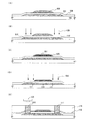
従来、ガラス基板上の薄膜トランジスタ(以下「TFT」ともいう。)によって構成される、所謂アクティブマトリクス駆動方式の液晶表示パネルは、半導体集積回路の製造技術と同様に、フォトマスクを使った光露光工程により、各種薄膜をパターニングすることにより製造されてきた。 Conventionally, a so-called active matrix liquid crystal display panel composed of thin film transistors (hereinafter also referred to as “TFTs”) on a glass substrate is a light exposure process using a photomask, as in the manufacturing technology of a semiconductor integrated circuit. Thus, it has been manufactured by patterning various thin films.
これまで、一枚のマザーガラス基板から複数の液晶表示パネルを切り出して、大量生産を効率良く行う生産技術が採用されてきた。マザーガラス基板のサイズは、1990年初頭における第1世代の300×400mmから、2000年には第4世代となり680×880mm若しくは730×920mmへと大型化して、一枚の基板から多数の表示パネルが取れるように生産技術が進歩してきた。 Until now, a production technique has been adopted in which a plurality of liquid crystal display panels are cut out from a single mother glass substrate and mass production is efficiently performed. The size of the mother glass substrate was increased from 300 x 400 mm of the first generation in early 1990 to the fourth generation in 2000 and increased to 680 x 880 mm or 730 x 920 mm. Production technology has progressed so that
ガラス基板若しくは表示パネルのサイズが小さい場合には、露光装置により比較的簡便にパターニング処理を行うことが可能であったが、基板サイズが大型化するにつれ、1回の露光処理で表示パネルの全面を同時に処理することが不可能となっていた。その結果、フォトレジストが塗布された領域を複数の領域に分割して、所定のブロック領域毎に露光処理を行い、順次それを繰り返して基板全面の露光を行う方法などが開発されてきた(例えば、特許文献1参照。)。 When the size of the glass substrate or the display panel is small, the patterning process can be performed relatively easily by the exposure apparatus. However, as the substrate size increases, the entire surface of the display panel can be obtained by a single exposure process. Cannot be processed simultaneously. As a result, a method has been developed in which a region coated with a photoresist is divided into a plurality of regions, an exposure process is performed for each predetermined block region, and the entire substrate is exposed by sequentially repeating the exposure process (for example, , See Patent Document 1).
また、アクティブマトリクス型のLCDやEL表示装置に用いられる、複数のTFTからなるアクティブマトリクス基板を形成するにあたり、TFTのドレイン領域の端部に集中する電界を緩和し、所謂ホットキャリア(ホットエレクトロン又はホットホール)効果を抑制するために、ソース、ドレイン領域の端部に形成された比較的低濃度の不純物領域(LDD領域;Lightly Doped Drain Regions)を設ける技術が用いられている(例えば、特許文献2参照。)。
しかしながら、ガラス基板のサイズは、第5世代で1000×1200mm若しくは1100×1300mmへとさらに大型化し、第6世代では1500×1800mm、第7世代では2000×2200mm、第8世代では2500×3000mm級、若しくはそれ以上のサイズが想定されるにつけ、従来のパターニング方法のみによるプロセスでは、生産性良く、低コストで表示パネルを製造することが困難となってきた。すなわち、つなぎ露光により多数回の露光処理を行えば処理時間は増大し、基板の大型化に対応することが困難となってきた。 However, the size of the glass substrate is further increased to 1000 × 1200 mm or 1100 × 1300 mm in the fifth generation, 1500 × 1800 mm in the sixth generation, 2000 × 2200 mm in the seventh generation, 2500 × 3000 mm class in the eighth generation, In addition, when a larger size is assumed, it is difficult to manufacture a display panel with high productivity and low cost by a process using only a conventional patterning method. That is, if exposure processing is performed many times by continuous exposure, the processing time increases, and it has become difficult to cope with an increase in the size of the substrate.
また、TFTにLDD領域を設ける場合には、半導体膜に注入される不純物に濃度差を設けるために、マスクとなる絶縁膜を別途形成したり、ゲート電極層の形状を工夫したりする必要があり、パターニング工程が自ずと増加してしまい、工程が複雑なものとなっていた。また、工程が増加するにつれて、当然乍ら、装置稼働コストや材料コストが嵩み、また、重金属や絶縁物等を含む多量の廃液を処理することが要求されるという問題点が内在していた。 Further, in the case where an LDD region is provided in a TFT, it is necessary to separately form an insulating film serving as a mask or to devise the shape of the gate electrode layer in order to provide a concentration difference in impurities implanted into the semiconductor film. In addition, the patterning process naturally increases, and the process becomes complicated. In addition, as the number of processes increases, there are naturally problems that the operating cost of the apparatus and the material cost increase, and that it is required to process a large amount of waste liquid containing heavy metals and insulators. .
本発明は、このような状況に鑑みてなされたものであり、簡略化された工程で作製可能なTFTに代表される半導体装置、及び該半導体装置を含む液晶表示装置及びEL表示装置、並びにそれらの作製方法を提供することを目的としている。特に、LDD領域を有するTFTを用いた半導体装置、及び該半導体装置を含む液晶表示装置及びEL表示装置を簡略化された工程で提供することを目的としている。 The present invention has been made in view of such a situation, and a semiconductor device typified by a TFT that can be manufactured by a simplified process, a liquid crystal display device and an EL display device including the semiconductor device, and those It is an object to provide a manufacturing method. In particular, it is an object to provide a semiconductor device using a TFT having an LDD region, a liquid crystal display device including the semiconductor device, and an EL display device in a simplified process.
上記課題を解決するため、本発明に係る半導体装置は、チャネル領域、一対の不純物領域及び一対の低濃度不純物領域からなる半導体層と、ゲート絶縁膜を介して、前記半導体層に接して形成された、膜厚差を有する単層構造又は積層構造のゲート電極層を含むことを特徴としている。 In order to solve the above problems, a semiconductor device according to the present invention is formed in contact with a semiconductor layer including a channel region, a pair of impurity regions, and a pair of low-concentration impurity regions, and a gate insulating film. In addition, a gate electrode layer having a single layer structure or a stacked structure having a difference in film thickness is included.
そして、前記一対の低濃度不純物領域は、膜厚差を有するゲート電極層のうち、膜厚の薄い方の領域に重なって形成されていることを特徴としている。 The pair of low-concentration impurity regions are formed so as to overlap a region having a smaller thickness in the gate electrode layer having a thickness difference.
また、上記課題を解決するため、本発明に係る半導体装置の作製方法は、半導体層上にゲート絶縁膜を形成し、前記ゲート絶縁膜上に、膜厚差を有する単層構造又は積層構造のゲート電極層を形成し、前記ゲート電極層をマスクとして、前記半導体層に不純物を導入することにより、一対の不純物領域及び一対の低濃度不純物領域を形成することを特徴としている。 In order to solve the above problems, a method for manufacturing a semiconductor device according to the present invention includes a gate insulating film formed over a semiconductor layer, and a single-layer structure or a stacked structure having a film thickness difference over the gate insulating film. A gate electrode layer is formed, and a pair of impurity regions and a pair of low-concentration impurity regions are formed by introducing impurities into the semiconductor layer using the gate electrode layer as a mask.
そして、前記一対の低濃度不純物領域は、膜厚差を有するゲート電極層のうち、膜厚の薄い方の領域に重なるように形成されることを特徴としている。 The pair of low-concentration impurity regions are formed so as to overlap with a region having a smaller thickness in the gate electrode layer having a thickness difference.
また、上記課題を解決するため、本発明に係る半導体装置の作製方法は、半導体層上にゲート絶縁膜を形成し、前記ゲート絶縁膜上にゲート電極層を形成し、前記ゲート電極層の焼成前後における幅の変化を利用して、前記半導体層中に濃度の異なる不純物元素を導入し、一対の不純物領域及び一対の低濃度不純物領域を形成することを特徴としている。 In order to solve the above problems, a method for manufacturing a semiconductor device according to the present invention includes forming a gate insulating film over a semiconductor layer, forming a gate electrode layer over the gate insulating film, and firing the gate electrode layer. A feature is that impurity elements having different concentrations are introduced into the semiconductor layer by utilizing a change in width before and after, thereby forming a pair of impurity regions and a pair of low-concentration impurity regions.
本発明は、膜厚差を有する単層構造又は積層構造のゲート電極層を含むことを特徴としているため、該ゲート電極層の膜厚差を利用して、低濃度不純物領域を容易に形成することができる。しかも、一度の不純物元素のドーピングによって、不純物領域と低濃度不純物領域を同時に作製することも可能である。これによって、ゲート電極層に低濃度不純物領域がオーバーラップした構造(Lov構造)を有するTFTのごとき半導体装置を容易に作成することができる。 Since the present invention includes a gate electrode layer having a single layer structure or a stacked structure having a film thickness difference, a low-concentration impurity region is easily formed using the film thickness difference of the gate electrode layer. be able to. In addition, the impurity region and the low-concentration impurity region can be formed simultaneously by doping the impurity element once. As a result, a semiconductor device such as a TFT having a structure in which a low concentration impurity region overlaps the gate electrode layer (Lov structure) can be easily formed.
また、本発明は、膜厚差を有する単層構造又は積層構造のゲート電極層を含むことを特徴としているが、このようなゲート電極層は、特に液滴吐出法を採用することによって、簡単に形成することができ、液滴吐出法の持つ利便性を最大限に活かすことができる。 Further, the present invention is characterized in that it includes a gate electrode layer having a single layer structure or a stacked structure having a film thickness difference. Such a gate electrode layer can be simplified by adopting a droplet discharge method in particular. The convenience of the droplet discharge method can be utilized to the maximum.
また、本発明において、液滴吐出法を積極的に採用することにより、工程を簡略化し、材料コストの削減を図ることができ、かつ、スループット、歩留まりの高い半導体装置、及びそれを含んだ発光装置(代表的には、EL表示装置)、液晶表示装置を提供することができる。特に、ガラス基板のサイズが、第6世代(1500×1800mm)、第7世代(2000×2200mm)、第8世代(2500×3000mm級)、若しくはそれ以上のサイズと拡大して行っても、生産性良く、低コストで表示パネルを製造することができる。また、導電材料としての重金属等を含む多量の廃液を処理する必要がなく、環境への配慮という観点からも、本発明は有意なものである。 In addition, in the present invention, by adopting the droplet discharge method positively, the process can be simplified, the material cost can be reduced, and a semiconductor device with high throughput and high yield, and light emission including the same A device (typically, an EL display device) or a liquid crystal display device can be provided. In particular, even if the size of the glass substrate is increased to the sixth generation (1500 × 1800 mm), the seventh generation (2000 × 2200 mm), the eighth generation (2500 × 3000 mm class), or larger, the production A display panel can be manufactured with good performance at low cost. Further, it is not necessary to treat a large amount of waste liquid containing heavy metal as a conductive material, and the present invention is significant from the viewpoint of environmental considerations.
以下、本発明の実施形態について図面を参照しながら説明する。但し、本発明は多くの異なる態様で実施することが可能であり、本発明の趣旨及びその範囲から逸脱することなくその形態及び詳細を様々に変更することができる。例えば、本実施形態及び本実施例の各々を適宜組み合わせて本発明を実施することができる。 Hereinafter, embodiments of the present invention will be described with reference to the drawings. However, the present invention can be implemented in many different modes, and various changes can be made in form and details without departing from the spirit and scope of the present invention. For example, the present invention can be implemented by appropriately combining each of the present embodiment and this example.
また本発明は、積極的に液滴吐出法等のマスクレスプロセスを用いて、あらゆる半導体装置の作製方法、液晶表示装置の作製方法及びEL表示装置の作製方法を提供するものであるが、すべての工程をマスクレスプロセスによって行う必要はなく、少なくとも一部の工程にマスクレスプロセスが含まれていればよい。したがって、以下、液滴吐出法のみの工程を示した場合であっても、従来のパターニング工程をはじめとする他の作製方法に代替できるものとする。 In addition, the present invention provides a method for manufacturing any semiconductor device, a method for manufacturing a liquid crystal display device, and a method for manufacturing an EL display device by positively using a maskless process such as a droplet discharge method. It is not necessary to perform this process by a maskless process, and it is sufficient that the maskless process is included in at least a part of the processes. Therefore, hereinafter, even when only a droplet discharge method is shown, it can be replaced with another manufacturing method including a conventional patterning step.
(実施形態1)
本実施形態は、図1、2を参照して、本発明に係る半導体装置の構成及びその作製方法の一実施形態について説明する。ここでは、トップゲート型TFTを例に挙げて説明する。
(Embodiment 1)
In the present embodiment, an embodiment of a configuration of a semiconductor device and a manufacturing method thereof according to the present invention will be described with reference to FIGS. Here, a top gate TFT will be described as an example.
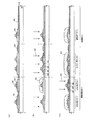
まず、基板100上に、半導体層101を形成する(図1(A))。半導体層101としては、アモルファス半導体、結晶性半導体、又はセミアモルファス半導体で形成する。いずれも、シリコン、シリコンゲルマニウム(SiGe)等を主成分とする半導体膜を用いることができる。また、特に、シリコンを主成分とするセミアモルファス半導体を、SAS(セミアモルファスシリコン)、又は、微結晶シリコン、マイクロクリスタルシリコンという。また、半導体層101は、CVD法やスパッタ法等によって形成することができる。なお、半導体層101の膜厚は、10〜100nmとするのが望ましい。また、シリコンウエハ、SOI基板(SIMOX基板等)のような基板を用いて、半導体層101を形成しても良い。
First, the
結晶性半導体膜を用いる場合、アモルファス半導体膜をニッケル等の触媒を含む溶液で処理した後、500〜750℃の熱結晶化工程によって結晶質シリコン半導体膜を得、さらにレーザー結晶化を行って結晶性の改善を施すことによって得ることができる。また、ジシラン(Si2H6)とフッ化ゲルマニウム(GeF4)の原料ガスとして、LPCVD(減圧CVD)法によって、多結晶半導体膜を直接形成することによっても、結晶性半導体膜を得ることができる。ガス流量比は、Si2H6/GeF4=20/0.9、成膜温度は400〜500℃、キャリアガスとしてHe又はArを用いたが、ガス流量比、成膜温度、及びキャリアガスはこれらの条件に限定されるものではない。 When a crystalline semiconductor film is used, after processing the amorphous semiconductor film with a solution containing a catalyst such as nickel, a crystalline silicon semiconductor film is obtained by a thermal crystallization process at 500 to 750 ° C., and further crystallized by laser crystallization. It can be obtained by improving the sex. A crystalline semiconductor film can also be obtained by directly forming a polycrystalline semiconductor film by LPCVD (low pressure CVD) as a source gas of disilane (Si 2 H 6 ) and germanium fluoride (GeF 4 ). it can. The gas flow rate ratio is Si 2 H 6 / GeF 4 = 20 / 0.9, the film formation temperature is 400 to 500 ° C., and He or Ar is used as the carrier gas, but the gas flow ratio, film formation temperature, and carrier gas are used. Is not limited to these conditions.
なお、基板100としては、ガラス基板、石英基板、アルミナなど絶縁物質で形成される基板、後工程の処理温度に耐え得る耐熱性を有するプラスチック基板等を用いることができる。この場合、酸化シリコン(SiOx)、窒化シリコン(SiNx)、酸化窒化シリコン(SiOxNy)(x>y)、窒化酸化シリコン(SiNxOy)(x>y)など(x、y=1、2・・・)、基板側から不純物などの拡散を防止するための下地絶縁膜を形成しておいてもよい。また、ステンレスなどの金属または半導体基板などの表面に酸化シリコンや窒化シリコンなどの絶縁膜を形成した基板なども用いることができる。
Note that as the
次に、半導体層101上にレジスト102を形成する(図1(A))。レジスト102は、ノズル120からレジスト材料を含む組成物を吐出することによって形成するのがよい。ただし、従来のように、レジスト102をパターニング形成しても良い。そして、レジスト102をマスクとして、半導体層101をエッチングすることにより、島状半導体層103を形成する(図1(B))。エッチング用ガスとしては、Cl2、BCl3、SiCl4もしくはCCl4などを代表とする塩素系ガス、CF4、SF6、NF3、CHF3などを代表とするフッ素系ガス、あるいはO2を用いたが、これらに限定されるものではない。なお、該エッチングは、大気圧プラズマを利用してもよい。
Next, a resist 102 is formed over the semiconductor layer 101 (FIG. 1A). The resist 102 is preferably formed by discharging a composition containing a resist material from the
次に、島状半導体層103上に、ゲート絶縁膜104を形成する(図1(B))。ゲート絶縁膜としては、酸化珪素(SixOy、例えばSiO2)、窒化珪素(SixNy、例えばSi3N4)、酸化窒化珪素(SiOxNy又はSiNxOy)、アルミナ(Al2O3)、酸化タンタル(Ta2O5)、酸化ランタン(La2O3)、酸化ハフニウム(HfO2)、酸化ジルコニウム(ZrO2)、シリケイト(ZrAlxOy)、アルミネート(HfAlxOy)等のあらゆる絶縁膜を利用することができる。また、これらの材料を2層以上に積層させた構造としてもよい。
Next, the
次に、ゲート絶縁膜104上に、第1の導電材料を含む組成物を、ノズル121を用いて液滴吐出法によって吐出することにより、第1のゲート電極層105を形成する(図1(C))。
Next, a first
次に、第1のゲート電極層105上に、第2の導電材料を含む組成物を、ノズル122を用いて液滴吐出法によって吐出することにより、第2のゲート電極層106を形成する(図1(D))。ここでは、図1(D)に示すように、第2のゲート電極層106は、第1のゲート電極層105よりも、幅が狭くなるようにする。また、第2のゲート電極層106は、第1のゲート電極層105よりも、幅が広くなるようし、第2のゲート電極層106が、第1のゲート電極層105を完全に覆うように形成してもよい。
Next, the second
いずれにせよ、後に説明する不純物元素のドーピング工程において、第1のゲート電極層105をスルーして、低濃度不純物領域が形成される。
In any case, a low concentration impurity region is formed through the first
なお、ここでは、第1及び第2のゲート電極層を形成するにあたり、異なるノズル121、122を用いたが、同じノズルを用いて、吐出条件を変えて第1及び第2のゲート電極層を形成しても良い。
Here,
第1及び第2のゲート電極層の膜厚については、特に制限はない。しかし、第2のゲート電極層106の幅を、第1のゲート電極層105の幅よりも狭くする場合においては、第1のゲート電極層105は、不純物を半導体層に注入しやすいようにできるだけ薄膜とし、第2のゲート電極層106は、チャネル領域に不純物が注入されないようにできるだけ厚膜としておくのが望ましい。一方、第2のゲート電極層106の幅を、第1のゲート電極層105の幅よりも広くする場合においては、その逆とすればよい。なお、チャネル領域に不純物が注入されないように、第1又は第2のゲート電極層は積層構造としても良い。
There are no particular restrictions on the thickness of the first and second gate electrode layers. However, in the case where the width of the second
なお、液滴吐出法とは、所定の導電材料を含む組成物を細孔から吐出して所定のパターンを形成する方法を意味し、代表的には、インクジェット法が挙げられるが、これに限定されるものではなく、ディスペンス法、スクリーン印刷やオフセット印刷等も含まれる。なお、以下、組成物としては、導電材料の他、半導体材料、有機半導体材料、絶縁材料(有機、無機共に含む。)、有機材料、無機材料等、液滴吐出法で吐出形成可能なあらゆる材料を含まれるものとする。ここで、有機材料、無機材料の代表的なものとして、LCDの配向膜や、カラーフィルタ、スペーサ、EL発光素子における発光層、電子輸送層、電子注入層、正孔輸送層、正孔注入層、カラーフィルタ等が挙げられる。以下、これらの材料を含む組成物を、インク、液滴、ペースト(特に、ナノ(nm)オーダーのサイズの材料を含む場合は、ナノペースト)と呼ぶことがある。 Note that the droplet discharge method means a method of forming a predetermined pattern by discharging a composition containing a predetermined conductive material from the pores, and typically includes an inkjet method, but is not limited thereto. In addition, dispensing methods, screen printing, offset printing, and the like are also included. Hereinafter, as the composition, any material that can be discharged and formed by a droplet discharge method, such as a conductive material, a semiconductor material, an organic semiconductor material, an insulating material (including both organic and inorganic), an organic material, and an inorganic material. Is included. Here, as typical organic materials and inorganic materials, LCD alignment films, color filters, spacers, light emitting layers in EL light emitting elements, electron transport layers, electron injection layers, hole transport layers, hole injection layers And color filters. Hereinafter, a composition containing these materials may be referred to as an ink, a droplet, or a paste (in particular, a nano paste when a material having a nano (nm) order size is included).
また、第1又は第2の導電材料としては、導電膜の機能に応じて種々の材料を選択することができる。代表的なものとしては、AgCu、Au、Ni、Pt、Cr、Al、W、Ta、Mo、Zn、Fe、In、Ti、Si、Ge、スズ(Sn)、パラジウム(Pd)、イリジウム(Ir)、ロジウム(Rh)、ルテニウム(Ru)、レニウム(Re)、テルル(Te)、カドミウム(Cd)、ジルコニウム(Zr)、バリウム(Ba)、アンチモン鉛、酸化スズ・アンチモン、フッ素ドープ酸化亜鉛、炭素、グラファイト、グラッシーカーボン、リチウム、ベリリウム、ナトリウム、マグネシウム、カリウム、カルシウム、スカンジウム、マンガン、ジルコニウム、ガリウム、ニオブ、ナトリウム−カリウム合金、マグネシウム/銅混合物、マグネシウム/銀混合物、マグネシウム/アルミニウム混合物、マグネシウム/インジウム混合物、アルミニウム/酸化アルミニウム混合物、リチウム/アルミニウム混合物等、ハロゲン化銀の微粒子等、又は分散性ナノ粒子、あるいは、透明導電膜として用いられる酸化インジウムスズ(ITO:Indium Tin Oxide)、ITOに珪素又は酸化珪素を含有させた導電材料(ITSO:Indium Tin Silicon Oxide)、酸化亜鉛(ZnO:Zinc Oxide)、ガリウムを添加した酸化亜鉛(GZO)、酸化インジウムに2〜20%の酸化亜鉛を混合した酸化インジウム亜鉛(IZO:Indium Zinc Oxide)、有機インジウム、有機スズ、窒化チタン、またはAl、C、Niの合金等を用いることができる。 Various materials can be selected as the first or second conductive material depending on the function of the conductive film. Typical examples include AgCu, Au, Ni, Pt, Cr, Al, W, Ta, Mo, Zn, Fe, In, Ti, Si, Ge, tin (Sn), palladium (Pd), iridium (Ir ), Rhodium (Rh), ruthenium (Ru), rhenium (Re), tellurium (Te), cadmium (Cd), zirconium (Zr), barium (Ba), antimony lead, tin / antimony oxide, fluorine-doped zinc oxide, Carbon, graphite, glassy carbon, lithium, beryllium, sodium, magnesium, potassium, calcium, scandium, manganese, zirconium, gallium, niobium, sodium-potassium alloy, magnesium / copper mixture, magnesium / silver mixture, magnesium / aluminum mixture, magnesium / Indium mixture, a Minium / aluminum oxide mixture, lithium / aluminum mixture, etc., silver halide fine particles or the like, or dispersible nanoparticles, or indium tin oxide (ITO) used as a transparent conductive film, ITO or silicon oxide Indium Tin Oxide (ITSO: Indium Tin Oxide), Zinc Oxide (ZnO), Zinc Oxide with Addition of Gallium (GZO), Indium Zinc Oxide Mixed with 2-20% Zinc Oxide (IZO: Indium Zinc Oxide), organic indium, organic tin, titanium nitride, an alloy of Al, C, Ni, or the like can be used.
なお、銅を用いる場合には、不純物対策のため、合わせてバリア膜を設けるとよい。溶媒は、酢酸ブチル、酢酸エチル等のエステル類、イソプロピルアルコール、エチルアルコール等のアルコール類、メチルエチルケトン、アセトン等の有機溶剤等を用いればよい。ここで、銅を配線として用いる場合のバリア膜としては、窒化シリコン、酸化窒化シリコン、窒化アルミニウム、窒化チタン、窒化タンタル(TaN:Tantalum Nitride)など窒素を含む絶縁性又は導電性の物質を用いると良く、これらを液滴吐出法で形成しても良い。 Note that when copper is used, a barrier film may be provided as a countermeasure against impurities. As the solvent, esters such as butyl acetate and ethyl acetate, alcohols such as isopropyl alcohol and ethyl alcohol, organic solvents such as methyl ethyl ketone and acetone may be used. Here, as a barrier film in the case of using copper as a wiring, an insulating or conductive material containing nitrogen such as silicon nitride, silicon oxynitride, aluminum nitride, titanium nitride, or tantalum nitride (TaN) is used. These may be formed by a droplet discharge method.
なお、ここでは、第1及び第2のゲート電極層を異なる材料で(例えば、第1のゲート電極層をTaN、第2のゲート電極層をW)形成したが、同材料で形成してもよい。また、これらの線幅や長さに応じて適宜材料を異ならせても良い。例えば、図1(C)、(D)における第1のゲート電極層のような比較的面積の大きな領域は、CuやAlのような安価な材料を用い、第2のゲート電極層は低抵抗のAgを用いることができる。 Here, the first and second gate electrode layers are formed of different materials (for example, the first gate electrode layer is TaN and the second gate electrode layer is W). Good. Further, the materials may be appropriately changed according to the line width and length. For example, a relatively large area such as the first gate electrode layer in FIGS. 1C and 1D uses an inexpensive material such as Cu or Al, and the second gate electrode layer has a low resistance. Ag can be used.
以上述べた液滴吐出手段に用いる組成物を吐出するためのノズルの径は、0.1〜50μm(好適には0.6〜26μm、)に設定し、ノズルから吐出される組成物の吐出量は0.00001pl〜50pl(好適には0.0001〜40pl)に設定するのがよい。この吐出量は、ノズルの径の大きさに比例して増加する。また、被処理物とノズル吐出口との距離は、所望の箇所に液滴を滴下するために、できる限り近づけておくことが好ましく、好適には0.1〜2mm程度に設定する。なお、ノズル径を変えずとも、圧電素子に印可されるパルス電圧を変えることによって吐出量を制御することもできる。これらの吐出条件は、ゲート電極層の線幅が約10μm以下となるように設定しておくのが望ましい。 The diameter of the nozzle for discharging the composition used for the droplet discharge means described above is set to 0.1 to 50 μm (preferably 0.6 to 26 μm), and the composition discharged from the nozzle is discharged. The amount is preferably set to 0.00001 pl to 50 pl (preferably 0.0001 to 40 pl). This discharge amount increases in proportion to the size of the nozzle diameter. In addition, the distance between the object to be processed and the nozzle outlet is preferably as close as possible in order to drop the liquid droplets at a desired location, and is preferably set to about 0.1 to 2 mm. In addition, the ejection amount can be controlled by changing the pulse voltage applied to the piezoelectric element without changing the nozzle diameter. These discharge conditions are preferably set so that the line width of the gate electrode layer is about 10 μm or less.
なお、液滴吐出法に用いる組成物の粘度は300mPa・s以下が好適であり、これは、乾燥を防止し、吐出口から組成物を円滑に吐出できるようにするためである。なお、用いる溶媒や用途に合わせて、組成物の粘度、表面張力等は適宜調整するとよい。一例として、ITO、ITSO、有機インジウム、有機スズを溶媒に溶解又は分散させた組成物の粘度は5〜50mPa・s、銀を溶媒に溶解又は分散させた組成物の粘度は5〜20mPa・s、金を溶媒に溶解又は分散させた組成物の粘度は10〜20mPa・sである。 Note that the viscosity of the composition used for the droplet discharge method is preferably 300 mPa · s or less, in order to prevent drying and to smoothly discharge the composition from the discharge port. Note that the viscosity, surface tension, and the like of the composition may be appropriately adjusted according to the solvent to be used and the application. For example, the viscosity of a composition in which ITO, ITSO, organic indium, or organic tin is dissolved or dispersed in a solvent is 5 to 50 mPa · s, and the viscosity of a composition in which silver is dissolved or dispersed in a solvent is 5 to 20 mPa · s. The viscosity of a composition in which gold is dissolved or dispersed in a solvent is 10 to 20 mPa · s.
各ノズルの径や所望のパターン形状などに依存するが、ノズルの目詰まり防止や高精細なパターンの作製のため、導電材料の粒子の径はなるべく小さい方が好ましく、好適には粒径0.1μm以下が好ましい。組成物は、電解法、アトマイズ法又は湿式還元法等の公知の方法で形成されるものであり、その粒子サイズは、一般的に約0.5〜10μmである。ただし、ガス中蒸発法で形成すると、分散剤で保護されたナノ分子は約7nmと微細であり、またこのナノ粒子は、被覆剤を用いて各粒子の表面を覆うと、溶剤中に凝集がなく、室温で安定に分散し、液体とほぼ同じ挙動を示す。したがって、被覆剤を用いることが好ましい。 Although depending on the diameter of each nozzle and the desired pattern shape, the diameter of the conductive material particles is preferably as small as possible for preventing nozzle clogging and producing a high-definition pattern. 1 μm or less is preferable. The composition is formed by a known method such as an electrolytic method, an atomizing method, or a wet reduction method, and its particle size is generally about 0.5 to 10 μm. However, when formed in a gas evaporation method, the nanomolecules protected by the dispersant are as fine as about 7 nm, and the nanoparticles are aggregated in the solvent when the surface of each particle is covered with a coating agent. And stably disperse at room temperature and shows almost the same behavior as liquid. Therefore, it is preferable to use a coating agent.
また、一導電材料の周囲を他の導電材料で覆った粒子を含む組成物を吐出形成して、ゲート電極層を形成してもよい。この際、両導電材料の間にバッファ層を設けておくのが望ましい。例えば、図19に示すように、Cu310の周りをAg311で覆った粒子(図19(A))において、Cu310とAg311の間にNi又はNiB(ニッケルボロン)からなるバッファ層312を設けた粒子構造が挙げられる(図19(B))。
Alternatively, the gate electrode layer may be formed by discharging a composition containing particles in which one conductive material is covered with another conductive material. At this time, it is desirable to provide a buffer layer between the two conductive materials. For example, as shown in FIG. 19, a particle structure in which a buffer layer 312 made of Ni or NiB (nickel boron) is provided between
なお、第1及び第2のゲート電極層は、上記組成物を吐出した後、一般的には加熱処理を行って形成される。例えば、100℃、3分間の乾燥を行い、さらに窒素及び/又は酸素を含む雰囲気下において、200〜350℃で15分間〜30分間の焼成を行うことにより形成する。この加熱処理は、第1の導電材料、第2の導電材料を吐出する毎に行っても良いし、第1の導電材料、第2の導電材料を吐出した後に一度に行っても良い。 Note that the first and second gate electrode layers are generally formed by performing heat treatment after discharging the composition. For example, the film is formed by drying at 100 ° C. for 3 minutes and further baking at 200 to 350 ° C. for 15 to 30 minutes in an atmosphere containing nitrogen and / or oxygen. This heat treatment may be performed every time the first conductive material and the second conductive material are discharged, or may be performed at a time after the first conductive material and the second conductive material are discharged.
ここで、ゲート電極層を液滴吐出法によって形成する場合、その後の加熱処理によって、ゲート電極層の膜厚が、減少するメカニズムについて説明する。 Here, in the case where the gate electrode layer is formed by a droplet discharge method, a mechanism by which the film thickness of the gate electrode layer is reduced by the subsequent heat treatment will be described.
ゲート電極層を液滴吐出法によって形成する場合、ノズルから吐出される組成物(液滴)は、一般的に、ゲート電極層を構成する導電材料を有機溶剤に分散又は溶解させたものであり、この他に組成物中には、分散剤や、バインダーと呼ばれる熱硬化性樹脂が含まれている。ここで、分散剤は、導電粒子を溶剤中に均一に分布させる働きを持ち、バインダーは、焼成時にクラックや不均一な焼きムラが発生するのを防止する働きを持つ。そして、乾燥又は焼成工程により、有機溶剤の蒸発、分散剤の分解除去及びバインダーによる硬化収縮が同時に進行することにより、導電粒子同士が融合し、組成物が硬化する。この際、導電粒子は、ナノレベルから数十〜百数十nmまで成長し、近接する成長粒子同士で融着、及び互いに連鎖することにより、金属連鎖体を形成する。一方、残った有機成分の殆ど(約80〜90%)は、金属連鎖体の外部に押し出され、結果として、金属連鎖体を含む導電層(ゲート電極層)と、その表面を覆う有機成分からなる層(以下、単に「有機層」という。)が形成される。 When the gate electrode layer is formed by a droplet discharge method, the composition (droplet) discharged from the nozzle is generally obtained by dispersing or dissolving a conductive material constituting the gate electrode layer in an organic solvent. In addition, the composition contains a dispersant and a thermosetting resin called a binder. Here, the dispersant has a function of uniformly distributing the conductive particles in the solvent, and the binder has a function of preventing generation of cracks and uneven baking during firing. Then, by the drying or baking step, evaporation of the organic solvent, decomposition and removal of the dispersant, and curing shrinkage by the binder proceed simultaneously, so that the conductive particles are fused and the composition is cured. At this time, the conductive particles grow from the nano level to several tens to hundreds of tens of nanometers, and are fused together and chained together to form a metal chain. On the other hand, most of the remaining organic components (about 80 to 90%) are pushed out of the metal chain, and as a result, from the conductive layer (gate electrode layer) containing the metal chain and the organic component covering the surface. A layer (hereinafter simply referred to as “organic layer”) is formed.
そして、導電ペーストを窒素及び酸素を含む雰囲気下で焼成すると、気体中に含まれる酸素(加熱雰囲気中に大気成分として含まれる酸素も含む。)と有機層中に含まれる炭素や水素などとが反応することにより、有機層を除去することができる。また、焼成雰囲気下に酸素が含まれていない場合には、別途、酸素プラズマ処理等によって有機層を除去することができる。 When the conductive paste is fired in an atmosphere containing nitrogen and oxygen, oxygen contained in the gas (including oxygen contained as an atmospheric component in the heating atmosphere) and carbon, hydrogen, etc. contained in the organic layer. By reacting, the organic layer can be removed. Further, when oxygen is not contained in the firing atmosphere, the organic layer can be removed separately by oxygen plasma treatment or the like.
このように、導電ペーストを窒素及び/又は酸素を含む雰囲気下で焼成、又は乾燥後、酸素プラズマで処理することによって、有機層は除去されるため、ゲート電極層の膜厚及び幅を減少させ、かつ、残存したゲート電極層の平滑化、薄膜化、低抵抗化を図ることができる。 In this way, the conductive layer is baked or dried in an atmosphere containing nitrogen and / or oxygen, and then treated with oxygen plasma to remove the organic layer, thereby reducing the thickness and width of the gate electrode layer. In addition, the remaining gate electrode layer can be smoothed, thinned, and reduced in resistance.
なお、導電材料を含む組成物を減圧下で吐出することにより組成物中の溶媒が揮発するため、後の加熱処理(乾燥又は焼成)時間を短縮することもできる。なお、前記雰囲気中における酸素の組成比を10〜25%とすると、効率良くゲート電極層の膜厚及び幅を減少させることができる。また、よりゲート電極層の平滑化、薄膜化、低抵抗化を図ることができる。 Note that since the solvent in the composition is volatilized by discharging the composition containing the conductive material under reduced pressure, the time for subsequent heat treatment (drying or baking) can be shortened. Note that when the oxygen composition ratio in the atmosphere is 10 to 25%, the thickness and width of the gate electrode layer can be efficiently reduced. In addition, the gate electrode layer can be made smoother, thinner, and lower in resistance.
次に、第1のゲート電極層105及び第2のゲート電極層106をマスクとして、島状半導体層103中に不純物元素109を、イオン注入法等によって導入する(図2(A))。不純物元素109は、n型の不純物元素でも、p型の不純物元素でもよい。n型の不純物元素としては、例えば、リン(P)、砒素(As)、アンチモン(Sb)を用いることができる。また、p型の不純物元素としては、例えば、硼素(B)を用いることができる。
Next, the
不純物元素109の導入により、島状半導体層103のうち、第1のゲート電極層105及び第2のゲート電極層106と重ならない部分には、一対の不純物領域110が形成される。一方、島状半導体層103のうち、第1のゲート電極層105のみと重なる部分には、不純物元素109が第1のゲート電極層105をスルーして導入されることによって、一対の低濃度不純物領域111が形成される。一対の不純物領域110は、ソース領域又はドレイン領域を構成する。また、一対の低濃度不純物領域111の間は、チャネル領域112となる(図2(A))。
By introduction of the
ここで、低濃度不純物領域は、トランジスタにおけるソース又はドレイン領域の端部に集中する電界を緩和し、所謂ホットキャリア(ホットエレクトロン又はホットホール)効果を抑制するために、ソース又はドレイン領域の端部に形成された比較的低濃度の不純物領域である。なお、ソース又はドレイン領域(高濃度不純物領域)と、低濃度不純物領域とに注入される不純物は、同じでも異なっていても良い。低濃度不純物領域の代表的なものとして、LDD領域(Lightly Doped Drain)がある。また、ドレイン近傍の電界を緩和するために、比較的浅い高濃度領域と、それを取り巻く低濃度領域からなる、所謂二重ドレイン構造(Double Diffused Drain : DDD)を有するトランジスタがあるが、DDDにおける低濃度領域も、上記低濃度不純物領域に含まれるものとする。 Here, the low-concentration impurity region relaxes the electric field concentrated on the end portion of the source or drain region in the transistor, and suppresses the so-called hot carrier (hot electron or hot hole) effect so as to suppress the end portion of the source or drain region. Is a relatively low-concentration impurity region. Note that the impurity implanted into the source or drain region (high concentration impurity region) and the low concentration impurity region may be the same or different. As a typical low-concentration impurity region, there is an LDD region (Lightly Doped Drain). In addition, in order to alleviate the electric field in the vicinity of the drain, there is a transistor having a so-called double drain structure (DDD) composed of a relatively shallow high-concentration region and a low-concentration region surrounding the high-concentration region. The low concentration region is also included in the low concentration impurity region.
次に、第2のゲート電極層106上にTFTを保護するためのキャップ絶縁膜113を形成する(図2(B))。材質は、ゲート絶縁膜104と同様のものを用いることができるが、O、C、Na等の不純物の混入を防止するためには、窒化珪素膜又は酸化窒化珪素膜を用いるのが望ましい。キャップ絶縁膜113は、必須ではないが、TFTを不純物の混入から保護するために、できるだけ形成しておくのが望ましい。
Next, a
次に、第2のゲート電極層106上に(キャップ絶縁膜113を形成した場合にはその上に)層間絶縁膜114を基板全面に形成する(図2(B))。層間絶縁膜114としては、ポリイミド、アクリル、ポリアミド、レジスト又はベンゾシクロブテン等の感光性又は非感光性の有機材料や、シロキサン(シリコンと酸素との結合で骨格構造が構成され、置換基に少なくとも水素を含む有機基(例えばアルキル基、芳香族炭化水素)、フルオロ基、または少なくとも水素を含む有機基とフルオロ基を用いたもの)等の耐熱性有機樹脂、を用いることができる。また、これらの材料に、カーボンブラック(CB)を混入させても良い。
Next, an
形成方法としては、その材料に応じて、スピンコート、ディップ、スプレー塗布、液滴吐出法(インクジェット法、ディスペンス法、スクリーン印刷、オフセット印刷等)、ドクターナイフ、ロールコーター、カーテンコーター、ナイフコーター等を採用することができる。あるいは、塗布法により得られるSOG膜(例えば、アルキル基を含むSiOx膜)を用いることもできる。また、無機材料を用いてもよく、その際には、酸化珪素、窒化珪素、酸化窒化珪素、DLC(ダイヤモンドライクカーボン)或いは窒化炭素(CN)等の炭素を有する膜、PSG(リンガラス)、BPSG(リンボロンガラス)、アルミナ膜等を用いることができる。形成方法としては、プラズマCVD法、減圧CVD(LPCVD)法、大気圧プラズマCVD等を用いることができる。なお、これらの絶縁膜を積層させてもよい。 As a forming method, depending on the material, spin coating, dipping, spray coating, droplet discharge method (inkjet method, dispensing method, screen printing, offset printing, etc.), doctor knife, roll coater, curtain coater, knife coater, etc. Can be adopted. Alternatively, an SOG film obtained by a coating method (for example, an SiOx film containing an alkyl group) can also be used. In addition, an inorganic material may be used, in which case silicon oxide, silicon nitride, silicon oxynitride, a film containing carbon such as DLC (diamond-like carbon) or carbon nitride (CN), PSG (phosphorus glass), BPSG (phosphorus boron glass), an alumina film, or the like can be used. As a formation method, a plasma CVD method, a low pressure CVD (LPCVD) method, an atmospheric pressure plasma CVD, or the like can be used. Note that these insulating films may be stacked.
次に、パターニング形成されたレジストをマスクとして、層間絶縁膜114、キャップ絶縁膜113及びゲート絶縁膜104をエッチングし、コンタクトホール115を開孔する(図2(C))。ここでは、プラズマエッチングを採用し、エッチング用ガスとしては、Cl2、BCl3、SiCl4もしくはCCl4などを代表とする塩素系ガス、CF4、SF6、NF3、CHF3などを代表とするフッ素系ガス、あるいはO2を用いたが、これらに限定されるものではない。なお、該エッチングは、大気圧プラズマを利用してもよい。
Next, using the patterned resist as a mask, the
なお、層間絶縁膜114を基板全面に形成せずに、コンタクトホールを形成したい領域を残して、液滴吐出法によって選択的に形成しても良い。そのために、コンタクトホールを形成したい領域に、予めFAS(フルオロアルキルシラン)等の撥液性の有機膜を形成しておくことは有効である。
Note that the
次に、コンタクトホール115に、第3の導電材料をノズル123から液滴吐出法によって吐出することにより、ソース電極116及びドレイン電極117を形成する(図2(D))。第3の導電材料は、第1又は第2の導電材料として用いられるものと同様のものを選択することができる。
Next, the third conductive material is discharged from the
以上の工程を経て、低濃度不純物領域を有する、いわゆるLDD構造のトップゲート型TFTが完成する。 Through the above steps, a so-called LDD structure top gate type TFT having a low concentration impurity region is completed.
以上説明したように、本発明に係る半導体装置は、チャネル領域、一対の不純物領域及び一対の低濃度不純物領域からなる半導体層と、ゲート絶縁膜を介して、前記半導体層に接して形成された幅の異なる複数のゲート電極層と、を含み、前記一対の低濃度不純物領域は、前記複数のゲート電極層のうち、膜厚の薄い部分に重なって形成されていることを特徴としている。 As described above, the semiconductor device according to the present invention is formed in contact with the semiconductor layer through the gate insulating film and the semiconductor layer including the channel region, the pair of impurity regions, and the pair of low-concentration impurity regions. A plurality of gate electrode layers having different widths, wherein the pair of low-concentration impurity regions are formed so as to overlap a thin portion of the plurality of gate electrode layers.
また、本発明に係る半導体装置の作製方法は、半導体層上にゲート絶縁膜を形成し、前記ゲート絶縁膜上に、幅の異なる複数のゲート電極層を形成し、前記複数のゲート電極層をマスクとして、前記半導体層に不純物を導入することにより、一対の不純物領域及び一対の低濃度不純物領域を形成し、前記一対の低濃度不純物領域は、前記複数のゲート電極層のうち、膜厚の薄い部分に重なって形成されることを特徴としている。 Further, in the method for manufacturing a semiconductor device according to the present invention, a gate insulating film is formed over a semiconductor layer, a plurality of gate electrode layers having different widths are formed over the gate insulating film, and the plurality of gate electrode layers are formed. As a mask, a pair of impurity regions and a pair of low-concentration impurity regions are formed by introducing impurities into the semiconductor layer, and the pair of low-concentration impurity regions has a thickness of the plurality of gate electrode layers. It is characterized by being formed overlying a thin part.
本発明は、幅の異なる少なくとも2層からなるゲート電極層(ここでは、第1及び第2のゲート電極層)を含み、少なくとも2層からなるゲート電極層のうち幅の広い層に重なって、一対の低濃度不純物領域が形成されていることを特徴としている。これにより、少なくとも2層からなるゲート電極層は、特に液滴吐出法を採用することによって、簡単に形成することができ、液滴吐出法の持つ利便性を最大限に活かすことができる。また、少なくとも2層からなるゲート電極層をマスクとして、不純物元素を導入することにより、一対の不純物領域及び一対の低濃度不純物領域を簡単に形成することができる。 The present invention includes a gate electrode layer composed of at least two layers having different widths (here, the first and second gate electrode layers), and overlaps a wide layer among the gate electrode layers composed of at least two layers. A pair of low-concentration impurity regions is formed. As a result, at least two gate electrode layers can be easily formed by employing the droplet discharge method, and the convenience of the droplet discharge method can be utilized to the maximum. In addition, by introducing an impurity element using at least two gate electrode layers as a mask, a pair of impurity regions and a pair of low-concentration impurity regions can be easily formed.
なお、本実施形態では、半導体装置として、トップゲート型TFTを例に挙げて説明したが、本発明の適用はこれに限定されるものではない。例えば、半導体層の下部にゲート絶縁膜を介して他のゲート電極層を設けた構造を有するデュアルゲート型TFTについても本発明を適用することができる。 In the present embodiment, the top gate type TFT has been described as an example of the semiconductor device, but application of the present invention is not limited to this. For example, the present invention can be applied to a dual gate type TFT having a structure in which another gate electrode layer is provided under a semiconductor layer with a gate insulating film interposed therebetween.
(実施形態2)
本実施形態では、図3を参照して、本発明に係る半導体装置の構成及びその作製方法の一実施形態について説明する。ここでは、トップゲート型TFTを例に挙げて説明する。ゲート絶縁膜104を形成する工程までは、実施形態1と同様に行うことができる(図3(A))。
(Embodiment 2)
In the present embodiment, an embodiment of a structure of a semiconductor device and a manufacturing method thereof according to the present invention will be described with reference to FIG. Here, a top gate TFT will be described as an example. Up to the step of forming the
ゲート絶縁膜104を形成した後に、導電材料を含む組成物をノズル121から吐出することにより、ゲート電極層301を形成する(図3(A))。導電材料としては、実施形態1に示したものから選択することができる。また、ゲート電極層301は、上記組成物を吐出した後、一般的には加熱処理を行って形成される。例えば、100℃、3分間の乾燥を行い、さらに窒素及び/又は酸素を含む雰囲気下において、200〜350℃で15〜30分間の焼成を行うことによりゲート電極層301を形成する。
After the
次に、ゲート電極層301上に、レジスト302をゲート電極層301の略中央部に選択的に形成する(図3(B))。レジスト302は、液滴吐出法によって形成するのが望ましい。レジスト302を形成する箇所は、低濃度不純物領域の幅に応じて、設定すればよい。そして、レジスト302をマスクとして、ゲート電極層301をエッチングし、テーパー状の側面を有するゲート電極層303(本実施形態において、以下、単に「ゲート電極層303」という。)を形成する(図3(B))。
Next, a resist 302 is selectively formed over the
次に、ゲート電極層303及びレジスト302をマスクとして、島状半導体層103中に不純物元素109を、イオン注入法等によって導入(ドーピング)する(図3(C))。不純物元素109は、n型の不純物元素の場合、例えば、リン(P)、砒素(As)、アンチモン(Sb)、p型の不純物元素の場合、例えば、硼素(B)を用いることができる。
Next, using the
不純物元素109の導入により、島状半導体層103のうち、ゲート電極層303と重ならない部分には、一対の不純物領域110が形成される。一方、島状半導体層103のうち、ゲート電極層303のテーパー状の側面と重なる部分には、不純物元素109が該側面をスルーして導入されることによって、一対の低濃度不純物領域111が形成される。一対の不純物領域110は、ソース領域又はドレイン領域を構成する。また、一対の低濃度不純物領域111の間は、チャネル領域112となる(図3(C))。
With the introduction of the
なお、レジスト302を除去した後に、ドーピングを行うこともできるが、チャネル領域112へ不純物元素が導入されないように、レジスト302を残したまま、ドーピングを行うのが望ましい。
Note that doping can be performed after the resist 302 is removed; however, it is preferable to perform doping while leaving the resist 302 so that an impurity element is not introduced into the
次に、レジスト302を除去した後、又は残した状態で、ゲート電極層303上にTFTを保護するためのキャップ絶縁膜113及び層間絶縁膜114を実施形態1と同様の要領で形成する(図3(D))。そして、層間絶縁膜114、キャップ絶縁膜113及びゲート絶縁膜104をエッチングし、コンタクトホールを開孔した後、該コンタクトホールに、導電材料をノズル123から液滴吐出法によって吐出することにより、ソース電極116及びドレイン電極117を形成する(図3(D))。導電材料は、ゲート電極層として用いられるものと同様のものを選択することができる。
Next, after the resist 302 is removed or left, a
以上の工程を経て、低濃度不純物領域を有する、いわゆるLDD構造のトップゲート型TFTが完成する。 Through the above steps, a so-called LDD structure top gate type TFT having a low concentration impurity region is completed.
以上説明したように、本発明に係る半導体装置は、チャネル領域、一対の不純物領域及び一対の低濃度不純物領域からなる半導体層と、ゲート絶縁膜を介して、前記半導体層に接して形成されたテーパー状のゲート電極層と、を含み、前記一対の低濃度不純物領域は、前記ゲート電極層のうち、テーパー状の部分に重なって形成されていることを特徴としている。 As described above, the semiconductor device according to the present invention is formed in contact with the semiconductor layer through the gate insulating film and the semiconductor layer including the channel region, the pair of impurity regions, and the pair of low-concentration impurity regions. And the pair of low-concentration impurity regions are formed so as to overlap a tapered portion of the gate electrode layer.
また、本発明に係る半導体装置の作製方法は、半導体層上にゲート絶縁膜を形成し、前記ゲート絶縁膜上にゲート電極層を形成し、前記ゲート電極層上に形成された絶縁物をマスクとしてエッチングを行い、前記ゲート電極層をテーパー状とし、前記テーパー状のゲート電極層をマスクとして、前記半導体層に不純物を導入することにより、一対の不純物領域及び一対の低濃度不純物領域を形成し、前記一対の低濃度不純物領域は、前記ゲート電極層のうち、テーパー状の領域に重なって形成されることを特徴としている。 The method for manufacturing a semiconductor device according to the present invention includes forming a gate insulating film on a semiconductor layer, forming a gate electrode layer on the gate insulating film, and masking the insulator formed on the gate electrode layer. Etching is performed to form a pair of impurity regions and a pair of low-concentration impurity regions by forming the gate electrode layer into a tapered shape and introducing impurities into the semiconductor layer using the tapered gate electrode layer as a mask. The pair of low-concentration impurity regions are formed to overlap a tapered region of the gate electrode layer.
本発明は、テーパー状の側面を有するゲート電極層を含み、ゲート電極層のテーパー状の側面に重なって、一対の低濃度不純物領域が形成されていることを特徴としている。これにより、テーパー状のゲート電極層は、特に液滴吐出法を採用することによって、簡単に形成することができ、液滴吐出法の持つ利便性を最大限に活かすことができる。また、テーパー状のゲート電極層をマスクとして、不純物元素を導入することにより、一対の不純物領域及び一対の低濃度不純物領域を簡単に形成することができる。 The present invention is characterized in that it includes a gate electrode layer having a tapered side surface, and a pair of low-concentration impurity regions are formed so as to overlap the tapered side surface of the gate electrode layer. Thereby, the tapered gate electrode layer can be easily formed by adopting the droplet discharge method in particular, and the convenience of the droplet discharge method can be fully utilized. In addition, a pair of impurity regions and a pair of low-concentration impurity regions can be easily formed by introducing an impurity element using the tapered gate electrode layer as a mask.
なお、本実施形態では、半導体装置として、トップゲート型TFTを例に挙げて説明したが、本発明の適用はこれに限定されるものではない。例えば、デュアルゲート型TFTについても本発明を適用することができる。また、テーパー状とするためには、上述したように液滴吐出法で選択的にゲート電極層を形成した後、レジスト等の絶縁物で覆って、両端をテーパー状にエッチングしても良いし、異なる吐出量のノズルから、ゲート電極層を構成する導電材料を含む組成物を複数回吐出することにより段階的に形成してもよい。 In the present embodiment, the top gate type TFT has been described as an example of the semiconductor device, but application of the present invention is not limited to this. For example, the present invention can be applied to a dual gate TFT. In order to obtain a tapered shape, the gate electrode layer may be selectively formed by a droplet discharge method as described above, and then covered with an insulator such as a resist, and both ends may be etched into a tapered shape. Alternatively, it may be formed stepwise by discharging a composition containing a conductive material constituting the gate electrode layer a plurality of times from nozzles having different discharge amounts.
(実施形態3)
本実施形態では、図4を参照して、本発明に係る半導体装置の構成及びその作製方法の一実施形態について説明する。ここでは、トップゲート型TFTを例に挙げて説明する。ゲート電極層を構成する導電材料を含む組成物を液滴吐出法によって形成する工程までは、実施形態1、2と同様に行うことができる。
(Embodiment 3)
In the present embodiment, an embodiment of a structure of a semiconductor device and a manufacturing method thereof according to the present invention will be described with reference to FIG. Here, a top gate TFT will be described as an example. The steps up to the step of forming the composition containing the conductive material forming the gate electrode layer by a droplet discharge method can be performed in the same manner as in Embodiments 1 and 2.
導電材料を含む組成物を形成したら、乾燥処理を行い、組成物を固体化させ、ゲート電極層400とする(図4(A))。乾燥処理は、例えば、100℃、3分間の条件下で行う。
When a composition including a conductive material is formed, a drying process is performed to solidify the composition, whereby the
次に、耐熱性を有する絶縁物401(本実施形態において、以下、単に「絶縁物401」という。)を、ゲート電極層400の略中央部に選択的に形成する(図4(B))。絶縁物401は、液滴吐出法によって選択的に形成するのが望ましい。絶縁物401を形成する箇所は、低濃度不純物領域の幅に応じて、設定すればよい。
Next, an
耐熱性を有する絶縁物401の材料としては、代表的には、シロキサン等の耐熱性樹脂を用いることができる。ただし、耐熱性を有する、又は熱吸収性を有する材料であれば、絶縁物401の材料はこれに限定されるものではない。
As a material for the
次に、ゲート電極層400を絶縁物401で部分的に覆った状態で、加熱処理を行う。例えば、窒素及び/又は酸素を含む雰囲気下において、200〜350℃で15分間〜30分間の焼成を行う。
Next, heat treatment is performed with the
上記加熱処理によって、ゲート電極層400のうち、絶縁物401が形成されていない領域の膜厚は、減少する。そのメカニズムについては、実施形態1で説明したとおりである。なお、加熱雰囲気下に酸素が含まれていない場合、又は、有機成分からなる層(有機層)が残存している場合には、酸素プラズマ処理等によって有機層を除去することができる。
Through the heat treatment, the thickness of the
一方、ゲート電極層400のうち、絶縁物401で覆われた領域は、加熱処理中、絶縁物401によって保護されるため、その領域の膜厚は減少しない。
On the other hand, a region of the
かくして、部分的に絶縁物401で覆われたゲート電極層400を加熱処理することで、ゲート電極層400の絶縁物401で覆われた領域と覆われていない領域とで、膜厚が異なるゲート電極層402(本実施形態において、以下、単に「ゲート電極層402」という。)が形成される(図4(C))。なお、ゲート電極層402は、基本的には、単層からなるが、ゲート電極層400が多層の場合には、この限りでない。
Thus, by subjecting the
なお、ゲート電極層402全体の幅も、上記加熱処理によって減少するため、それを考慮に入れて、加熱処理前のゲート電極層400の吐出条件を制御するのが望ましい。
Note that the width of the entire
このように、ゲート電極層400を、絶縁物401で覆い、窒素及び/又は酸素を含む雰囲気下で焼成し、又は乾燥後、酸素プラズマで処理することによって、その表面部分の有機層は除去されるため、ゲート電極層の所望の領域の膜厚及び幅を減少させ、かつ、残存したゲート電極層の平滑化、薄膜化、低抵抗化を図ることができる。特に、前記雰囲気中における酸素の組成比を10〜25%とすると、効率良くゲート電極層の膜厚及び幅を減少させることができ、よりゲート電極層の平滑化、薄膜化、低抵抗化を図ることができる。
In this way, the
次に、ゲート電極層402及び絶縁物401をマスクとして、島状半導体層103中に不純物元素109を、イオン注入法等によって導入(ドーピング)する(図4(D))。不純物元素109は、n型の不純物元素の場合、例えば、リン(P)、砒素(As)、アンチモン(Sb)、p型の不純物元素の場合、例えば、硼素(B)を用いることができる。
Next, the
不純物元素109の導入により、島状半導体層103のうち、ゲート電極層402と重ならない部分には、一対の不純物領域110が形成される。一方、島状半導体層103のうち、ゲート電極層402の膜厚の薄い部分と重なる部分には、不純物元素109がその部分をスルーして導入されることによって、一対の低濃度不純物領域111が形成される。一対の不純物領域110は、ソース領域又はドレイン領域を構成する。また、一対の低濃度不純物領域111の間は、チャネル領域112となる(図4(D))。
With the introduction of the
なお、絶縁物401を除去した後に、ドーピングを行うこともできるが、チャネル領域112へ不純物元素が導入されないように、絶縁物401を残したまま、ドーピングを行うのが望ましい。
Note that doping can be performed after the
次に、絶縁物401を除去した後、又は残した状態で、ゲート電極層402上にTFTを保護するためのキャップ絶縁膜113、及び、層間絶縁膜114を実施形態1と同様の要領で形成する(図4(E))。そして、層間絶縁膜114、キャップ絶縁膜113及びゲート絶縁膜104をエッチングし、コンタクトホールを開孔した後、該コンタクトホールに、導電材料をノズル123から液滴吐出法によって吐出することにより、ソース電極116及びドレイン電極117を形成する(図4(E))。導電材料は、ゲート電極層として用いられるものと同様のものを選択することができる。
Next, after the
以上の工程を経て、低濃度不純物領域を有する、いわゆるLDD構造のトップゲート型TFTが完成する。 Through the above steps, a so-called LDD structure top gate type TFT having a low concentration impurity region is completed.
以上説明したように、本発明に係る半導体装置は、チャネル領域、一対の不純物領域及び一対の低濃度不純物領域からなる半導体層と、ゲート絶縁膜を介して前記半導体層に接して形成された、異なる膜厚を有する単層からなるゲート電極層と、を含み、前記一対の低濃度不純物領域は、前記ゲート電極層のうち、膜厚の薄い部分に重なって形成されていることを特徴としている。 As described above, the semiconductor device according to the present invention is formed in contact with the semiconductor layer through the gate insulating film and the semiconductor layer including the channel region, the pair of impurity regions, and the pair of low-concentration impurity regions. And the pair of low-concentration impurity regions are formed so as to overlap a thin portion of the gate electrode layer. .
また、本発明に係る半導体装置の作製方法は、半導体層上にゲート絶縁膜を形成し、前記ゲート絶縁膜上にゲート電極層を形成し、前記ゲート電極層上に耐熱性を有する絶縁物を形成し、前記ゲート電極層を酸素及び窒素を含む雰囲気中で加熱することにより、前記絶縁物が形成されていない部分のゲート電極層の膜厚を減少させ、異なる膜厚を有するゲート電極層とし、前記ゲート電極層をマスクとして、前記半導体層に不純物を導入することにより、一対の不純物領域及び一対の低濃度不純物領域を形成し、前記一対の低濃度不純物領域は、前記ゲート電極層のうち、膜厚の薄い部分に重なって形成されていることを特徴としている。 In addition, in the method for manufacturing a semiconductor device according to the present invention, a gate insulating film is formed over a semiconductor layer, a gate electrode layer is formed over the gate insulating film, and an insulating material having heat resistance is formed over the gate electrode layer. Forming and heating the gate electrode layer in an atmosphere containing oxygen and nitrogen to reduce the thickness of the gate electrode layer in a portion where the insulator is not formed, thereby forming gate electrode layers having different thicknesses. A pair of impurity regions and a pair of low concentration impurity regions are formed by introducing impurities into the semiconductor layer using the gate electrode layer as a mask, and the pair of low concentration impurity regions are formed in the gate electrode layer It is characterized in that it is formed so as to overlap with a thin portion.
本発明は、異なる膜厚を有する単層からなるゲート電極層を含み、一対の低濃度不純物領域は、前記ゲート電極層のうち、膜厚の薄い部分に重なって形成されていることを特徴としている。これにより、該ゲート電極層は、特に液滴吐出法を採用することによって、簡単に形成することができ、液滴吐出法の持つ利便性を最大限に活かすことができる。特に、液滴吐出法を用いて吐出した導電材料を含む組成物は、部分的に加熱処理を行うことによって、異なる膜厚を有する単層又は多層からなるゲート電極層を形成することができる。本発明は、この異なる膜厚を有するゲート電極層を利用して、その膜厚の薄い部分をスルーさせて不純物元素を導入することを特徴としており、一対の低濃度不純物領域を簡単に形成することができる。 The present invention includes a gate electrode layer composed of a single layer having different thicknesses, and the pair of low-concentration impurity regions are formed so as to overlap a thin portion of the gate electrode layer. Yes. As a result, the gate electrode layer can be easily formed especially by employing the droplet discharge method, and the convenience of the droplet discharge method can be utilized to the maximum. In particular, a composition including a conductive material discharged using a droplet discharge method can form a single-layer or multi-layer gate electrode layer having different thicknesses by partial heat treatment. The present invention is characterized in that an impurity element is introduced by using a gate electrode layer having a different film thickness to pass through a thin portion of the film thickness, and a pair of low-concentration impurity regions is easily formed. be able to.
なお、本実施形態では、半導体装置として、トップゲート型TFTを例に挙げて説明したが、本発明の適用はこれに限定されるものではない。例えば、デュアルゲート型TFTについても本発明を適用することができる。 In the present embodiment, the top gate type TFT has been described as an example of the semiconductor device, but application of the present invention is not limited to this. For example, the present invention can be applied to a dual gate TFT.
(実施形態4)
本実施形態では、図5を参照して、本発明に係る半導体装置の構成及びその作製方法の一実施形態について説明する。ここでは、トップゲート型TFTを例に挙げて説明する。ゲート電極層を構成する導電材料を含む組成物を液滴吐出法によって形成する工程までは、実施形態1、2と同様に行うことができる。
(Embodiment 4)
In the present embodiment, an embodiment of a structure of a semiconductor device and a manufacturing method thereof according to the present invention will be described with reference to FIG. Here, a top gate TFT will be described as an example. The steps up to the step of forming the composition containing the conductive material forming the gate electrode layer by a droplet discharge method can be performed in the same manner as in Embodiments 1 and 2.
導電材料を含む組成物を形成したら、乾燥処理を行い、又は室温にて放置し、組成物を固体化させ、ゲート電極層400とする(図5(A))。乾燥処理の場合は、例えば、100℃、3分間の条件下で行う。なお、ゲート電極層400は、単層でも多層でも良い。
After the composition containing the conductive material is formed, drying treatment is performed or the composition is left at room temperature to solidify the composition to form the gate electrode layer 400 (FIG. 5A). In the case of the drying treatment, for example, the drying is performed at 100 ° C. for 3 minutes. Note that the
次に、ゲート電極層400をマスクとして、島状半導体層103中に不純物元素109を、イオン注入法等によって導入(ドーピング)する(図5(B))。不純物元素109は、n型の不純物元素の場合、例えば、リン(P)、砒素(As)、アンチモン(Sb)、p型の不純物元素の場合、例えば、硼素(B)を用いることができる。
Next, using the
不純物元素109の導入により、島状半導体層103のうち、ゲート電極層400と重ならない部分には、一対の不純物領域110が形成される(図5(B))。一対の不純物領域110は、ソース領域又はドレイン領域を構成する。
With the introduction of the
次に、ゲート電極層400に対して加熱処理を行う。加熱処理としては、例えば、窒素及び/又は酸素を含む雰囲気下において、200〜350℃で15分間〜30分間の焼成を行う。この加熱処理によって、ゲート電極層400の幅及び膜厚が減少したゲート電極層500(本実施形態において、以下、単に「ゲート電極層500」という。)が形成される(図5(C))。ゲート電極層400の幅及び膜厚が減少するメカニズムについては、実施形態1で説明したとおりであり、加熱処理中に生じる有機層501を、窒素及び/又は酸素を含む雰囲気下において焼成、又は酸素プラズマ処理等によって除去することにより、ゲート電極層500が得られる。
Next, heat treatment is performed on the
このように、ゲート電極層400を、窒素及び/又は酸素を含む雰囲気下で焼成し、又は乾燥後、酸素プラズマで処理することによって、その表面部分の有機層は除去されるため、ゲート電極層の所望の領域の膜厚及び幅を減少させ、かつ、残存したゲート電極層の平滑化、薄膜化、低抵抗化を図ることができる。特に、前記雰囲気中における酸素の組成比を10〜25%とすると、効率良くゲート電極層の膜厚及び幅を減少させることができ、よりゲート電極層の平滑化、薄膜化、低抵抗化を図ることができる。
As described above, the
例えば、Agペーストを吐出し、窒素雰囲気、230℃、1hrで、ゲート電極層の焼成を行った場合、1100nm程度の膜厚となったゲート電極層が、さらに、窒素雰囲気に組成比25%の酸素を混合し、230℃、1hrのゲート電極層の焼成を行うことにより、700nm程度の膜厚に減少することが実験的に判った。減少率は、約63%である。また、線幅も、膜厚ほどの減少率はないが、2回目の焼成によって線幅が減少した。また、2回目の焼成によって、抵抗率は、60〜70μΩ・cmに低下した。したがって、1回目の焼成後に、高濃度の不純物をドーピングし、2回目の焼成によって、ゲート電極層の線幅及び膜厚が減少することを利用して、さらに低濃度の不純物をドーピングすることにより、低濃度不純物領域を形成することができる。この結果は、実施形態3においても、適用できる。 For example, when the Ag electrode is discharged and the gate electrode layer is baked in a nitrogen atmosphere at 230 ° C. for 1 hr, the gate electrode layer having a thickness of about 1100 nm is further added to the nitrogen atmosphere with a composition ratio of 25%. It was experimentally found that the film thickness was reduced to about 700 nm by mixing oxygen and baking the gate electrode layer at 230 ° C. for 1 hr. The reduction rate is about 63%. Also, the line width is not as low as the film thickness, but the line width was reduced by the second firing. The resistivity decreased to 60 to 70 μΩ · cm by the second firing. Therefore, by doping a high concentration impurity after the first baking, and by doping a lower concentration impurity by utilizing the fact that the line width and film thickness of the gate electrode layer are reduced by the second baking. A low concentration impurity region can be formed. This result can also be applied to the third embodiment.
次に、ゲート電極層500をマスクとして、島状半導体層103中に低濃度の不純物元素502を、イオン注入法等によって導入(ドーピング)する(図5(D))。低濃度の不純物元素502は、n型の不純物元素の場合、例えば、リン(P)、砒素(As)、アンチモン(Sb)、p型の不純物元素の場合、例えば、硼素(B)を用いることができる。
Next, using the
低濃度の不純物元素502の導入により、島状半導体層103のうち、ゲート電極層500と重ならない部分には、一対の低濃度不純物領域111が形成される(図5(D))。そして、一対の低濃度不純物領域111の間には、チャネル領域112となる。
With the introduction of the low-
なお、低濃度不純物領域111の幅は、ゲート電極層400が加熱処理によって減少する幅に依存するため、所望の低濃度不純物領域111の幅に合わせて、上記加熱処理条件を適宜調整すればよい。
Note that the width of the low-
次に、ゲート電極層500上にTFTを保護するためのキャップ絶縁膜113、及び、層間絶縁膜114を実施形態1と同様の要領で形成する(図5(E))。そして、層間絶縁膜114、キャップ絶縁膜113及びゲート絶縁膜104をエッチングし、コンタクトホールを開孔した後、該コンタクトホールに、導電材料をノズル123から液滴吐出法によって吐出することにより、ソース電極116及びドレイン電極117を形成する(図5(E))。導電材料は、ゲート電極層として用いられるものと同様のものを選択することができる。
Next, a
以上の工程を経て、低濃度不純物領域を有する、いわゆるLDD構造のトップゲート型TFTが完成する。 Through the above steps, a so-called LDD structure top gate type TFT having a low concentration impurity region is completed.
以上説明したように、本発明に係る半導体装置の作製方法は、半導体層上にゲート絶縁膜を形成し、前記ゲート絶縁膜上にゲート電極層を形成し、前記ゲート電極層をマスクとして、前記半導体層に不純物を導入することにより、一対の不純物領域を形成し、前記ゲート電極層を酸素及び窒素を含む雰囲気中で加熱することにより、前記ゲート電極層の膜厚及び幅を減少させ、前記膜厚及び幅が減少したゲート電極層をマスクとして、前記半導体層に低濃度の不純物を導入することにより、一対の低濃度不純物領域を形成することを特徴としている。 As described above, in the method for manufacturing a semiconductor device according to the present invention, a gate insulating film is formed over a semiconductor layer, a gate electrode layer is formed over the gate insulating film, and the gate electrode layer is used as a mask. By introducing impurities into the semiconductor layer, a pair of impurity regions is formed, and the gate electrode layer is heated in an atmosphere containing oxygen and nitrogen to reduce the thickness and width of the gate electrode layer, A feature is that a pair of low-concentration impurity regions are formed by introducing low-concentration impurities into the semiconductor layer using the gate electrode layer whose thickness and width are reduced as a mask.
本発明は、ゲート電極層を構成する導電材料を含む組成物に対し加熱処理を行うことによって、ゲート電極層の幅及び膜厚を減少させることができることを利用して、その加熱処理の前後に、ゲート電極層をマスクとして濃度の異なる不純物元素を導入することにより、簡単な工程で、半導体層中にソース、ドレイン領域及び一対の低濃度不純物領域を形成することができる。ゲート電極層は、特に液滴吐出法を採用することによって、簡単に形成することができるため、本発明は液滴吐出法の持つ利便性を最大限に活かすことができる。 The present invention utilizes the fact that the width and film thickness of the gate electrode layer can be reduced by performing heat treatment on the composition containing the conductive material constituting the gate electrode layer, before and after the heat treatment. By introducing impurity elements having different concentrations using the gate electrode layer as a mask, the source and drain regions and the pair of low-concentration impurity regions can be formed in the semiconductor layer with a simple process. Since the gate electrode layer can be easily formed especially by adopting a droplet discharge method, the present invention can make the most of the convenience of the droplet discharge method.
なお、本実施形態では、半導体装置として、トップゲート型TFTを例に挙げて説明したが、本発明の適用はこれに限定されるものではない。例えば、デュアルゲート型TFTについても本発明を適用することができる。 In the present embodiment, the top gate type TFT has been described as an example of the semiconductor device, but application of the present invention is not limited to this. For example, the present invention can be applied to a dual gate TFT.
本実施例では、図6を参照して、本発明に係る半導体装置の構成及びその作製方法において、下地前処理行う場合、特に、ゲート電極層の下部に接して親水性の膜を設ける場合について説明する。ここでは、トップゲート型TFTを例に挙げて説明する。図6(A)〜(C)において、ゲート絶縁膜104を形成する工程までは、上記実施形態と同様に行うことができる。
In this embodiment, with reference to FIGS. 6A and 6B, in the structure of the semiconductor device and the manufacturing method thereof according to the present invention, when base pretreatment is performed, particularly when a hydrophilic film is provided in contact with the lower portion of the gate electrode layer. explain. Here, a top gate TFT will be described as an example. 6A to 6C, the process up to the step of forming the
図6(A)は、導電体の酸化膜(ここでは、TiOx膜130)を基板全面又は少なくともゲート電極層が形成される領域に形成する場合を示している。TiOx(酸化チタン)膜としては、代表的には、光触媒としても用いられる二酸化チタンを用いるのがよい。その後、例えば、実施形態1の要領でゲート電極層105、106を形成する。 FIG. 6A shows a case where a conductive oxide film (here, a TiOx film 130) is formed over the entire surface of the substrate or at least in a region where a gate electrode layer is formed. As the TiOx (titanium oxide) film, it is typically preferable to use titanium dioxide that is also used as a photocatalyst. Thereafter, for example, the gate electrode layers 105 and 106 are formed in the same manner as in the first embodiment.
図6(B)は、導電膜(ここでは、Ti膜131)を全面に形成した後、例えば、実施形態1の要領でゲート電極層105、106を形成し、これらゲート電極層をマスクとして、Ti膜131の酸化処理(焼成又はO2イオン注入後に焼成等)を行い、ゲート電極層の周囲をTiOx膜130とする場合を示している。酸化処理は、例えば、Ti膜を1〜5nm成膜した後、230℃で焼成することによって行う。酸化処理を行うことにより、ゲート電極層同士のショートを防止することができる。 In FIG. 6B, after a conductive film (here, Ti film 131) is formed over the entire surface, for example, gate electrode layers 105 and 106 are formed in the same manner as in Embodiment 1, and these gate electrode layers are used as a mask. In this example, the Ti film 131 is oxidized (baked or baked after O 2 ion implantation) to form a TiOx film 130 around the gate electrode layer. The oxidation treatment is performed, for example, by baking a film at 230 ° C. after forming a Ti film having a thickness of 1 to 5 nm. By performing the oxidation treatment, a short circuit between the gate electrode layers can be prevented.
図6(C)は、Ti膜131を全面に形成した後、例えば、実施形態1の要領でゲート電極層105、106を形成し、ゲート電極層105をマスクとして、露出したTi膜131をエッチングする場合を示している。これにより、ゲート電極層同士のショートを防止することができる。
In FIG. 6C, after the Ti film 131 is formed on the entire surface, for example, the gate electrode layers 105 and 106 are formed as in the first embodiment, and the exposed Ti film 131 is etched using the
また、Ti以外にも、Sc(スカンジウム)、V(バナジウム)、Cr(クロム)、Mn(マンガン)、Fe(鉄)、Co(コバルト)、Ni(ニッケル)、Cu(銅)、Zn(亜鉛)等の所謂3d遷移元素や、W(タングステン)、Al(アルミニウム)、Ta(タンタル)、Zr(ジルコニウム)、Hf(ハフニウム)、Ir(イリジウム)、Nb(ニオブ)、Pd(パラジウム)、Pt(白金)、及びそれらの酸化物、窒化物、酸化窒化物を用いることもできる。これらの金属を直接基板全面に形成した場合には、図6(B)、(C)のように、ゲート電極層が形成される部分以外を除去又は酸化、窒化、酸化窒化することにより絶縁化する必要がある。 In addition to Ti, Sc (scandium), V (vanadium), Cr (chromium), Mn (manganese), Fe (iron), Co (cobalt), Ni (nickel), Cu (copper), Zn (zinc) So-called 3d transition elements such as W (tungsten), Al (aluminum), Ta (tantalum), Zr (zirconium), Hf (hafnium), Ir (iridium), Nb (niobium), Pd (palladium), Pt (Platinum) and oxides, nitrides, and oxynitrides thereof can also be used. When these metals are formed directly on the entire surface of the substrate, as shown in FIGS. 6B and 6C, insulation is achieved by removing or oxidizing, nitriding, and oxynitriding other than the portion where the gate electrode layer is formed. There is a need to.
なお、酸化チタンは、光触媒物質としても知られる材料であるが、他にも、チタン酸ストロンチウム(SrTiO3)、セレン化カドミウム(CdSe)、タンタル酸カリウム(KTaO3)、硫化カドミウム(CdS)、酸化ジルコニウム(ZrO2)、酸化ニオブ(Nb2O5)、酸化亜鉛(ZnO)、酸化鉄(Fe2O3)、酸化タングステン(WO3)等の光触媒物質を形成してもよい。また、これらの金属を主成分とする材料以外にも、ポリイミド、アクリル、シロキサン等の耐熱性樹脂を形成したり、プラズマ処理(好適には大気圧プラズマ)を施したりしてもよい。 Titanium oxide is a material also known as a photocatalytic substance. In addition, strontium titanate (SrTiO 3 ), cadmium selenide (CdSe), potassium tantalate (KTaO 3 ), cadmium sulfide (CdS), Photocatalytic substances such as zirconium oxide (ZrO 2 ), niobium oxide (Nb 2 O 5 ), zinc oxide (ZnO), iron oxide (Fe 2 O 3 ), and tungsten oxide (WO 3 ) may be formed. In addition to materials containing these metals as main components, a heat-resistant resin such as polyimide, acrylic, or siloxane may be formed, or plasma treatment (preferably atmospheric pressure plasma) may be performed.
上記導電体膜、及びその酸化物、窒化物、酸化窒化物の作製方法に特に制限はない。液滴吐出法やスプレー法等によって、直接基板全面に又は選択的に導電体膜、及びその酸化物、窒化物、酸化窒化物を形成しても良い。なお、TiOx膜130、Ti膜131等の親水性の膜を形成することにより、ゲート絶縁膜104と後に形成するゲート電極層との密着性を高めることもできる。なお、本実施例は、他の実施形態又は実施例と自由に組み合わせることができる。
There is no particular limitation on the method for manufacturing the conductor film and its oxide, nitride, and oxynitride. A conductor film and its oxide, nitride, or oxynitride may be formed directly or selectively on the entire surface of the substrate by a droplet discharge method, a spray method, or the like. Note that by forming a hydrophilic film such as the TiOx film 130 or the Ti film 131, adhesion between the
本実施例では、本発明に係る半導体装置の構成及びその作製方法において、半導体層101(又は島状半導体層103)として、SAS(セミアモルファスシリコン)を用いた場合について説明する。 In this embodiment, the case where SAS (semi-amorphous silicon) is used as the semiconductor layer 101 (or the island-shaped semiconductor layer 103) in the structure of the semiconductor device and the manufacturing method thereof according to the present invention will be described.
SASは、珪化物気体をグロー放電分解することにより得ることができる。代表的な珪化物気体としては、SiH4であり、その他にもSi2H6、SiH2Cl2、SiHCl3、SiCl4、SiF4などを用いることができる。この珪化物気体を水素、水素とヘリウム、アルゴン、クリプトン、ネオンから選ばれた一種または複数種の希ガス元素で希釈して用いることでSASの形成を容易なものとすることができる。希釈率は10〜1000倍の範囲で珪化物気体を希釈することが好ましい。勿論、グロー放電分解による被膜の反応生成は減圧下で行うが、圧力は概略0.1〜133Paの範囲で行えば良い。グロー放電を形成するための電力は1〜120MHz、好ましくは13〜60MHzの高周波電力を供給すれば良い。基板加熱温度は300℃以下が好ましく、100〜200℃の基板加熱温度が推奨される。 SAS can be obtained by glow discharge decomposition of a silicide gas. A typical silicide gas is SiH 4 , and in addition, Si 2 H 6 , SiH 2 Cl 2 , SiHCl 3 , SiCl 4 , SiF 4 and the like can be used. The formation of the SAS can be facilitated by diluting the silicide gas with one or plural kinds of rare gas elements selected from hydrogen, hydrogen and helium, argon, krypton, and neon. It is preferable to dilute the silicide gas in a dilution ratio of 10 to 1000 times. Of course, the reaction of the coating by glow discharge decomposition is performed under reduced pressure, but the pressure may be in the range of about 0.1 to 133 Pa. The power for forming the glow discharge may be high frequency power of 1 to 120 MHz, preferably 13 to 60 MHz. The substrate heating temperature is preferably 300 ° C. or lower, and a substrate heating temperature of 100 to 200 ° C. is recommended.
また、珪化物気体中に、CH4、C2H6などの炭化物気体、又はGeH4、GeF4などのゲルマニウム化気体を混入させて、エネルギーバンド幅を1.5〜2.4eV、若しくは0.9〜1.1eVに調節しても良い。 Further, a carbide gas such as CH 4 or C 2 H 6 or a germanium gas such as GeH 4 or GeF 4 is mixed in the silicide gas, so that the energy bandwidth is 1.5 to 2.4 eV, or 0. It may be adjusted to .9 to 1.1 eV.
また、SASは、価電子制御を目的とした不純物元素を意図的に添加しないときに弱いn型の電気伝導性を示す。これは、アモルファス半導体を成膜するときよりも高い電力のグロー放電を行うため酸素が半導体層中に混入しやすいためである。そこで、TFTのチャネル形成領域を設ける第1の半導体膜に対しては、p型を付与する不純物元素を、この成膜と同時に、或いは成膜後に添加することで、しきい値制御をすることが可能となる。p型を付与する不純物元素としては、代表的には硼素であり、B2H6、BF3などの不純物気体を1〜1000ppmの割合で珪化物気体に混入させると良い。例えば、p型を付与する不純物元素としてボロンを用いる場合、該ボロンの濃度を1×10¹⁴〜6×10¹⁶atoms/cm3とすると良い。なお、上記SASでチャネル領域を構成することにより1〜10cm2/V・secの電界効果移動度を得ることができる。なお、本実施例は、他の実施形態又は実施例と自由に組み合わせることができる。 SAS exhibits weak n-type conductivity when an impurity element for the purpose of valence electron control is not intentionally added. This is because oxygen is easily mixed into the semiconductor layer because glow discharge with higher power is performed than when an amorphous semiconductor is formed. Therefore, for the first semiconductor film provided with the channel formation region of the TFT, the threshold value is controlled by adding an impurity element imparting p-type at the same time as or after the film formation. Is possible. The impurity element imparting p-type is typically boron, and an impurity gas such as B 2 H 6 or BF 3 may be mixed in the silicide gas at a rate of 1 to 1000 ppm. For example, when boron is used as the impurity element imparting p-type conductivity, the concentration of boron is preferably 1 × 10 14 to 6 × 10 16 atoms / cm 3 . A field effect mobility of 1 to 10 cm 2 / V · sec can be obtained by configuring the channel region with the SAS. Note that this embodiment can be freely combined with other embodiment modes or embodiments.
本実施例では、主に図7〜図10を参照して、本発明を用いたアクティブマトリクス型EL発光装置の作製方法について説明する。 In this example, a method for manufacturing an active matrix EL light-emitting device using the present invention will be described mainly with reference to FIGS.
有機化合物又は無機化合物を含む層からなる発光素子(代表的にはエレクトロルミネセンス(EL:Electro Luminescence)を利用した発光素子)を、薄膜トランジスタ(TFT)で駆動させる場合、EL発光装置は図7に示すように、画素領域に設けられるスイッチング用TFTのON電流のバラツキを抑えるため、駆動用TFTを備えた、少なくとも2トランジスタ型の構造とするのが一般的である。 In the case where a light-emitting element (typically a light-emitting element using electroluminescence (EL)) including a layer containing an organic compound or an inorganic compound is driven by a thin film transistor (TFT), the EL light-emitting device is shown in FIG. As shown, in order to suppress variation in the ON current of the switching TFT provided in the pixel region, it is general to have at least a two-transistor structure including a driving TFT.
ここで、上記発光素子は、一対の電極間にキャリア輸送特性の異なる有機化合物又は無機化合物を含む層を積層し、一方の電極からは正孔を注入し、他方の電極からは電子を注入できるように形成され、一方の電極から注入された正孔と、他方の電極から注入された電子とが再結合して発光中心を励起して、それが基底状態に戻るときに光を放出する現象を利用した素子である。 Here, in the light-emitting element, a layer containing an organic compound or an inorganic compound having different carrier transport properties can be stacked between a pair of electrodes, holes can be injected from one electrode, and electrons can be injected from the other electrode. A phenomenon in which holes injected from one electrode and electrons injected from the other electrode recombine to excite the emission center and emit light when it returns to the ground state. It is an element using
なお、図7(B)は、発光素子を順積みにした場合の回路図であり、ここで順積み発光素子とは、駆動用TFT213の画素電極が正孔注入電極(陽極)となる場合をいう。なお、図8(B)は、発光素子を逆積みにした場合の回路図であり、ここで逆積み発光素子とは、駆動用TFT213の画素電極が電子注入電極(陰極)となる場合をいう。
Note that FIG. 7B is a circuit diagram in the case where light emitting elements are stacked in order. Here, the stacked light emitting element refers to a case where the pixel electrode of the driving
また、図7(B)の212はスイッチング用TFTであり、画素へ流れる電流のON/OFFを制御するものである。ここで、図7(A)からも分かるように、スイッチング用TFT212のドレイン配線225(又はソース配線)は、駆動用TFT213のゲート電極層226と接続された構成となるが、ゲート電極層226とドレイン配線225の層との間には、ゲート絶縁膜が存在するため、両者は、コンタクトホール115を介して、電気的に接続される。なお、以上の符号は、図8においても同様である。また、図7、8において、227はそれぞれ容量部を示しているが、容量部を形成する領域は、この領域に限定されない。なお、図7、8における符号は、図9、10と対応している。
Further,
本発明を用いた発光装置及びその作製方法について、図9、10を参照して説明する。図9は、図7(A)又は図8(A)のX−Yの断面構造を示したものである。なお、図9、10において、容量部227は省略した。本実施例では、実施形態2のテーパー状のゲート電極層を有するTFTを用いたアクティブマトリクス型EL発光装置について説明するが、ゲート電極層の構造は、これに限定されるものではなく、他の実施形態又は実施例に置換して、あるいはそれらを組み合わせて実施することが可能である。
A light-emitting device and a manufacturing method thereof using the present invention will be described with reference to FIGS. FIG. 9 shows a cross-sectional structure taken along line XY in FIG. 7A or FIG. 8A. In FIGS. 9 and 10, the
まず、基板100上に下地絶縁膜118を形成する。ここでは、SiNOとSiONの積層構造としたが(図9(A))、材質、構造ともにこれに限定されるものではない。上述したゲート絶縁膜に用いられる材料と同様のものから選択することができる。
First, the
次に、下地絶縁膜118上に、上記実施形態又は実施例に示した要領で、島状半導体層103及びゲート絶縁膜104を形成する(図9(A))。
Next, the island-shaped
さらに、実施形態2に示した要領で、レジスト302を用いてエッチングを行い、テーパー状のゲート電極層303を形成する(図9(A))。ここで、画素部215の駆動用TFT213のゲート電極層226は、スイッチング用TFT212と接続するため、スイッチング用TFT212の方向に延びている(図7(A)又は図8(A)参照)。したがって、図9(A)において、226と示したゲート電極層は、一般的に同一層からなる。なお、ゲート電極層226は、少なくとも不純物元素が導入される領域のみテーパー状にすれば足りる。また、上記ゲート電極層は、積層構造でも良い。
Further, etching is performed using the resist 302 in the manner described in Embodiment 2 to form a tapered gate electrode layer 303 (FIG. 9A). Here, the
次に、駆動回路部214のpチャネル型TFT211が形成される部分の上方に、レジスト200を形成した後に(レジスト200は、液滴吐出法によって形成するのが望ましい。)、ゲート電極層303、225をマスクとして、1015〜1017atoms/cm3オーダーのn型不純物元素201を島状半導体層103にドーピングする。これによって、駆動回路部214のnチャネル型TFT210、並びに画素部215のスイッチング用TFT212及び駆動用TFT213のゲート電極層で覆われていない島状半導体層には、ソース又はドレイン領域となるn型不純物領域202が形成される。さらに、ゲート電極層のテーパー状の部分と重なる領域には、n型の低濃度不純物領域203が形成される。さらにその間には、チャネル領域204が形成される(図9(B))。なお、特に、画素部215の駆動用TFT213については、後に形成される発光素子224の積層構造に応じて、nチャネル型TFT又はpチャネル型TFTを選択すればよい。
Next, after the resist 200 is formed above the portion where the p-channel TFT 211 of the driver circuit portion 214 is formed (the resist 200 is preferably formed by a droplet discharge method), the
ここで、n型不純物元素としては、砒素(As)、燐(P)などを用いることができる。その後、レジスト200は、O2アッシング等によって除去する。この際、ゲート電極層上にレジスト302が残存している場合には、このレジスト302も同時に除去される。 Here, arsenic (As), phosphorus (P), or the like can be used as the n-type impurity element. Thereafter, the resist 200 is removed by O 2 ashing or the like. At this time, if the resist 302 remains on the gate electrode layer, the resist 302 is also removed at the same time.
次に、駆動回路部214のnチャネル型TFT210及び画素部215のスイッチング用TFT212及び駆動用TFT213になる領域をレジスト205で覆った後(レジスト205は、液滴吐出法によって形成するのが望ましい。)、ゲート電極層303をマスクとして、1015〜1017atoms/cm3オーダーのp型不純物元素206を、pチャネル型TFT211の島状半導体層にドーピングする。これによって、pチャネル型TFT211のソース又はドレイン領域となるp型不純物領域207が形成される。さらに、ゲート電極層のテーパー状の部分と重なる領域には、p型の低濃度不純物領域208が形成される。さらにその間には、チャネル領域209が形成される(図9(C))。ここで、p型不純物元素としては、硼素(B)などを用いることができる。その後、レジスト205は、O2アッシング等によって除去する。この際、pチャネル型TFT211のゲート電極層上に、レジスト302が残存している場合には、このレジスト302も同時に除去される。
Next, the regions to be the n-channel TFT 210 in the driver circuit portion 214, the switching
なお、上記ドーピングを行った後、熱処理によって該不純物元素の活性化を行ってもよい。 Note that after the doping, the impurity element may be activated by heat treatment.
次に、TFTを覆うキャップ絶縁膜113をプラズマCVD法により形成する(図10(A))。キャップ絶縁膜113としては、窒化珪素膜又は酸化窒化珪素膜を用いるのがよいが、材料はこれに限定されるものではない。また、形成方法もプラズマCVD法に限定されるものではない。なお、TFT上方からの不純物の混入を防止するため、キャップ絶縁膜113はできるだけ形成しておくのが望ましい。
Next, a
また、図示しないが、ソース、ドレイン配線上に、TFT上方からの不純物の拡散等を防止するためのパッシベーション膜を形成しておくのが望ましい。パッシベーション膜は、プラズマCVD法又はスパッタリング法などの薄膜形成法を用い、窒化珪素、酸化珪素、窒化酸化珪素、酸化窒化珪素、酸化窒化アルミニウム、または酸化アルミニウム、ダイヤモンドライクカーボン(DLC)、窒素含有炭素(CN)、その他の絶縁性材料を用いて形成することができる。なお、これらの材料を積層させて形成してもよい。なお、該パッシベーション膜は、絶縁体材料の微粒子を含む組成物を液滴吐出法によって吐出することによっても形成することができる。 Although not shown, it is desirable to form a passivation film for preventing diffusion of impurities from above the TFT on the source and drain wirings. The passivation film is formed using a thin film formation method such as plasma CVD or sputtering, and silicon nitride, silicon oxide, silicon nitride oxide, silicon oxynitride, aluminum oxynitride, or aluminum oxide, diamond-like carbon (DLC), nitrogen-containing carbon (CN) and other insulating materials can be used. Note that these materials may be stacked. Note that the passivation film can also be formed by discharging a composition containing fine particles of an insulator material by a droplet discharge method.
次に、半導体層に添加された不純物元素の活性化のための加熱処理を行う。この活性化は、N2雰囲気にした炉中において500〜800℃に加熱することによって行う。例えば、RTA(ラピッドサーマルアニール)法を用いることができる。または、レーザー光を半導体層に照射して活性化を行ってもよい。この場合、基板裏面側又は基板表面側からのみレーザー光を照射してもよいし、基板表面及び裏面の両側から照射してもよい。なお、工程を簡略化したい場合には、該活性化処理を省略してもよい。 Next, heat treatment for activating the impurity element added to the semiconductor layer is performed. This activation is performed by heating to 500 to 800 ° C. in a furnace having an N 2 atmosphere. For example, an RTA (rapid thermal annealing) method can be used. Alternatively, activation may be performed by irradiating the semiconductor layer with laser light. In this case, the laser beam may be irradiated only from the substrate rear surface side or the substrate front surface side, or from both sides of the substrate front surface and the rear surface. In addition, when it is desired to simplify the process, the activation process may be omitted.
なお、その後、水素を含む窒化珪素膜または窒化酸化珪素膜からなる絶縁膜をプラズマCVD法により形成し、該絶縁膜から水素を放出させ、半導体層の水素化を行うための加熱処理を行い、シリコンの不対結合手を終端させてもよい。この加熱処理は、クリーンオーブンを用い、N2雰囲気下において350〜450℃(好ましくは、410℃)で行えばよい。なお、該絶縁膜としては、他の水素及び珪素を含む絶縁膜を用いてもよいし、形成方法もプラズマCVD法以外の方法を用いてもよい。 After that, an insulating film made of a silicon nitride film or a silicon nitride oxide film containing hydrogen is formed by a plasma CVD method, hydrogen is released from the insulating film, and heat treatment is performed to hydrogenate the semiconductor layer. Silicon dangling bonds may be terminated. This heat treatment may be performed at 350 to 450 ° C. (preferably 410 ° C.) in a N 2 atmosphere using a clean oven. Note that another insulating film containing hydrogen and silicon may be used as the insulating film, and a method other than the plasma CVD method may be used as a forming method.
次に、キャップ絶縁膜113上に、層間絶縁膜114を形成する。ここでは、ポリイミドを含む溶液をスピンコート法によって基板全面に塗布したが、この材料、方法に限定されるものではない。例えば、ポリイミド系樹脂の他にも、アクリル系樹脂、ポリアミド系樹脂、または珪素、酸素、水素からなる化合物のうちSi−O−Si結合を含む無機シロキサン、珪素に結合されている水素がメチルやフェニルのような有機基に置換された有機シロキサン系の絶縁膜等を用いることができる。また、液滴吐出法によって層間絶縁膜114を形成することもできる。
Next, an
次に、層間絶縁膜114、キャップ絶縁膜113、ゲート絶縁膜104を選択的に除去し、コンタクトホールを開孔する。水素化処理のための絶縁膜が形成されている場合にはこれも除去する。コンタクトホール開孔は、レジストを基板全面に塗布した後にプリベークを行い、露光、現像プロセスを経てマスクパターンを形成し、マスクパターンをエッチングしてコンタクトホールを形成するという従来の方法を用いることができるが、レジストを液滴吐出法によって選択的に吐出することによりマスクパターンを形成する方が、コスト削減、工程簡略化という観点から望ましい。
Next, the
コンタクトホールを形成した後、画素電極216を形成する(図10(B))。画素電極216は、液滴吐出法によって形成しても良いし、パターニング工程を経て形成しても良い。なお、画素電極216は、コンタクトホールを開孔する前に形成しても良い。
After the contact hole is formed, the
次に、コンタクトホールを介して、各TFTのソース領域、ドレイン領域に接続される配線217、228等を形成する(図10(B))。ここで、配線217は、スイッチング用TFT212のソース又はドレイン領域と、駆動用TFT213のゲート電極層とを接続する配線である。また、配線228は、駆動用TFT213のソース又はドレイン領域と、画素電極216とを接続する配線である。これら配線は、導電材料を含む組成物を吐出することによって形成するのが望ましい。導電材料としては、Ag、Au、Cu、Ni、Pt、Pd、Ir、Rh、W、Al、Ta、Mo、Cd、Zn、Fe、Ti、Si、Ge、Zr、Ba等の金属、Al、C、Niの合金、ハロゲン化銀の微粒子等、又は分散性ナノ粒子等を用いることができる。
Next,
なお、これら配線は多層構造とすることもできる。例えば、厚さ50〜200nmのTi膜、厚さ250〜400nmのAl膜又はAl−Si合金膜、厚さ50〜200nmのTi膜を積層させて、配線を形成する。また、三層構造のうち、TiをTiN、又は窒素を50%以下の組成比で含む窒化チタン(本明細書では、窒素を50%以下の組成比で含む窒化チタンをTi(N)と表す)で置き換えてもよいし、TiN又はTi(N)を新たに積層させた構造としてもよい。また、Alは150〜200℃でヒロックが発生してしまうため、Siを含有させておくことが望ましい。このように、特にAlを用いる場合、ITOとダイレクトコンタクトさせると、Alが腐食するという問題点があるが、AlとITOの間にTi(又はTiN)を介することにより、この問題点は解消できる。また、特にAl、C、Niの合金を用いる場合には、Ti等を介さなくとも、ITOとダイレクトコンタクトが可能になるという利点がある。 These wirings can also have a multilayer structure. For example, a Ti film having a thickness of 50 to 200 nm, an Al film or Al-Si alloy film having a thickness of 250 to 400 nm, and a Ti film having a thickness of 50 to 200 nm are stacked to form a wiring. In addition, of the three-layer structure, Ti is TiN or titanium nitride containing nitrogen at a composition ratio of 50% or less (in this specification, titanium nitride containing nitrogen at a composition ratio of 50% or less is represented as Ti (N). ) Or a structure in which TiN or Ti (N) is newly stacked. Moreover, since Al will generate hillocks at 150 to 200 ° C., it is desirable to contain Si. In this way, particularly when Al is used, there is a problem that Al is corroded if it is brought into direct contact with ITO, but this problem can be solved by using Ti (or TiN) between Al and ITO. . In particular, when an alloy of Al, C, and Ni is used, there is an advantage that direct contact with ITO is possible without using Ti or the like.
以上の工程により、nチャネル型TFT210及びpチャネル型TFT211からなるCMOS構造を含む駆動回路部214と、スイッチングTFT212及び駆動用TFT213及び容量部を含む画素部215からなるアクティブマトリクス基板が完成する(図10(C))。なお、本実施例においては、本発明に係る半導体装置を、駆動回路部及び画素部両方に用いたが、少なくとも一方に用いることもできる。
Through the above steps, a driving circuit portion 214 including a CMOS structure including an n-channel TFT 210 and a p-channel TFT 211 and an active matrix substrate including a switching
さらに、画素電極216上に、有機樹脂膜、無機絶縁膜を用いて形成された隔壁(土手、バンク等とも呼ばれる。)218を液滴吐出法によって選択的に形成する。隔壁218としては、シロキサン等の耐熱性樹脂、ポリイミド、アクリル等の樹脂を用いるのが望ましい。特に、シロキサンを用いることにより、後の真空ベーク工程を高温で行うことができ、EL素子に悪影響を及ぼす水分を十分に除去することができる。なお、隔壁218は、選択的に形成されることにより、開口部を有しており、該開口部において画素電極216が露出している。なお、隔壁218は、レジスト等を用いたパターニングによって形成しても良い。
Further, a partition wall (also referred to as a bank, a bank, or the like) 218 formed using an organic resin film or an inorganic insulating film is selectively formed over the
次に、隔壁218の開口部において画素電極216と接するように、有機化合物を含む層219(電界発光層)を形成する。有機化合物を含む層219は、単数の層で構成しても良いし、複数の層を積層させて構成しても良い。複数の層で構成する場合、半導体素子側(画素電極側)から見て、(1)陽極、ホール(正孔)注入層、ホール輸送層、発光層、電子輸送層、陰極、(2)陽極、ホール注入層、発光層、電子輸送層、陰極、(3)陽極、ホール注入層、ホール輸送層、発光層、電子輸送層、電子注入層、陰極、(4)陽極、ホール注入層、ホール輸送層、発光層、ホールブロッキング層、電子輸送層、陰極、(5)陽極、ホール注入層、ホール輸送層、発光層、ホールブロッキング層、電子輸送層、電子注入層、陰極、等の順に積層された素子構造とすればよい。これは、所謂順積みと呼ばれる構造で、画素電極216は、陽極(ホール注入電極)として機能する。一方、半導体素子側(画素電極側)から見て、陰極が先に来る場合には、逆積みと呼ばれ、画素電極216は陰極として機能する。
Next, a
次に、有機化合物を含む層219を覆うように、対向電極220を形成する。対向電極220は、発光層の積層方法により、陽極又は陰極として機能する。有機化合物を含む層219を画素電極216と対向電極220との間に挟むことにより、発光素子224が形成される。
Next, the
次に、有機化合物を含む層219(特に発光層)を水分から保護するために、パッシベーション膜221を形成する。これに代えて、あるいは、さらにパッシベーション膜221が外気に曝されないように気密性が高く、脱ガスの少ない保護フィルム(ラミネートフィルム、紫外線硬化樹脂フィルム等)やカバー材でパッケージング(封入)することが好ましい。本明細書でラミネートフィルムとは、基材フィルムと接着性合成樹脂フィルムとの積層フィルム、または2種類以上の積層フィルムを指す。基材フィルムとしては、PETやPBT等のポリエステル、ナイロン6、ナイロン66等のポリアミド、また無機蒸着フィルム、または紙類を用いればよい。また、接着性合成フィルムとしてはPEやPP等のポリオレフィン、アクリル系合成樹脂、エポキシ系合成樹脂などを用いればよい。ラミネートフィルムはラミネート装置により、被処理体と熱圧着によりラミネートされる。なお、ラミネート工程を行う前処理としてアンカーコート剤を塗布することが好ましく、ラミネートフィルムと被処理体との接着を強固なものとすることができる。アンカーコート剤としてはイソシアネート系材料などを用いればよい。最後に、絶縁物222を介して、封止基板223でアクティブマトリクス基板を封止した。
Next, a
以上の工程により、EL発光装置が完成する(図10(C))。EL発光装置は、その発光方向により、ボトムエミッション型、トップエミッション型、デュアルエミッション型に大別される。以下、それぞれにおける画素電極216及び対向電極220をも含めた発光素子の構造について説明する。
Through the above steps, an EL light-emitting device is completed (FIG. 10C). EL light-emitting devices are roughly classified into a bottom emission type, a top emission type, and a dual emission type according to the emission direction. Hereinafter, the structure of the light emitting element including the
ボトムエミッション型の場合、画素電極216(この場合、正孔注入電極)の材質は、透過性を有する金属、例えば、ITO、ITSO、ZnO、IZO、GZO等の透明導電膜を用いることができる。また、特にITSOを用いる場合には、濃度の異なる酸化珪素を含むITSOを積層させることによって、TFTと画素電極216との接続間の低抵抗を維持しつつ、発光層への正孔注入効率を高めることができる。一方、陰極(電子注入電極)となる対向電極220の材質は、仕事関数の小さいCa、Al、CaF、MgAg、AlLi等を用いることができる。
In the case of the bottom emission type, the material of the pixel electrode 216 (in this case, the hole injection electrode) can be a transparent metal, for example, a transparent conductive film such as ITO, ITSO, ZnO, IZO, or GZO. In particular, when ITSO is used, the efficiency of hole injection into the light-emitting layer can be improved while the low resistance between the connection between the TFT and the
トップエミッション型の場合、一般的には、ボトムエミッション型における正孔注入電極(画素電極216)と電子注入電極(対向電極220)を入れ替え、さらに有機化合物を含む層を逆積みとし、電流制御用TFTの極性を反転させることにより、基板と反対側(上側)に発光素子からの光を取り出すことのできるトップエミッション型発光装置が得られる。例えば、画素電極216としては、反射性を有する金属、例えば、Al、AlLi等を用い、対向電極220としては、光透過性のあるITO、ITSO、ZnO、IZO、GZO等の透明導電膜を用いることができる。
In the case of the top emission type, in general, the hole injection electrode (pixel electrode 216) and the electron injection electrode (counter electrode 220) in the bottom emission type are interchanged, and the layers containing organic compounds are reversely stacked to control current. By reversing the polarity of the TFT, a top emission type light emitting device capable of extracting light from the light emitting element on the opposite side (upper side) of the substrate can be obtained. For example, a reflective metal such as Al or AlLi is used for the
デュアルエミッション型の場合、正孔注入電極(画素電極216)の材質としては、ボトムエミッション型の場合と同様に、ITO、ITSO、ZnO、IZO、GZO等の透明導電膜を用いることもできる。電子注入電極(対向電極220)としては、発光層からの光を透過させるべく、1〜10nmの薄アルミニウム膜、もしくはLiを微量に含むアルミニウム膜等を用いることができる。これにより、上下に発光素子224からの光を取り出すことのできるデュアルエミッション型発光装置が得られる。なお、画素電極216と対向電極220の役割は入れ替えても良い。
In the case of the dual emission type, as the material of the hole injection electrode (pixel electrode 216), a transparent conductive film such as ITO, ITSO, ZnO, IZO, GZO or the like can be used as in the case of the bottom emission type. As the electron injection electrode (counter electrode 220), a thin aluminum film having a thickness of 1 to 10 nm, an aluminum film containing a small amount of Li, or the like can be used so as to transmit light from the light emitting layer. As a result, a dual emission type light emitting device capable of extracting light from the
なお、本実施例は、他の実施形態、実施例と自由に組み合わせることができる。 Note that this embodiment can be freely combined with other embodiments and examples.
実施例3によって作製されるアクティブマトリクス型EL発光装置を含むEL表示パネル901を用いて、ELテレビ受像機を完成させることができる。図11は、ELテレビ受像機の主要な構成を示すブロック図を示している。EL表示パネル901には、(1)実施例3のように、表示パネルの画素部と走査線側駆動回路903を基板上に一体形成し、さらに信号線側駆動回路902を別途ドライバICとして実装する場合、(2)表示パネルの画素部のみが形成されて走査線側駆動回路903と信号線側駆動回路902とがTAB方式により実装される場合、(3)表示パネルの画素部とその周辺に走査線側駆動回路903と信号線側駆動回路902とがCOG方式により実装される場合、などがあるが、どのような形態としても良い。
An EL television receiver can be completed using the
その他の外部回路の構成として、映像信号の入力側では、チューナ904で受信した信号のうち、映像信号を増幅する映像信号増幅回路905と、そこから出力される信号を赤、緑、青の各色に対応した色信号に変換する映像信号処理回路906と、その映像信号をドライバICの入力仕様に変換するためのコントロール回路907などからなっている。コントロール回路907は、走査線側と信号線側にそれぞれ信号が出力する。デジタル駆動する場合には、信号線側に信号分割回路908を設け、入力デジタル信号をm個に分割して供給する構成としても良い。
As other external circuit configurations, on the input side of the video signal, among the signals received by the
チューナ904で受信した信号のうち、音声信号は、音声信号増幅回路909に送られ、その出力は音声信号処理回路910を経てスピーカ913に供給される。制御回路911は受信局(受信周波数)や音量の制御情報を入力部912から受け、チューナ904や音声信号処理回路910に信号を送出する。
Of the signals received by the
このような外部回路と、EL表示パネル901を筐体に組みこんで、図20(A)に示すようなテレビ受像機を完成させることができる。勿論、本発明はテレビ受像機に限定されず、パーソナルコンピュータのモニタをはじめ、鉄道の駅や空港などにおける情報表示盤や、街頭における広告表示盤など特に大面積の表示媒体として様々な用途に適用することができる。なお、本実施例は、他の実施形態、実施例と自由に組み合わせることができる。
A television receiver as shown in FIG. 20A can be completed by incorporating such an external circuit and the
本実施例では、図12〜16を参照して、本発明を用いたアクティブマトリクス型液晶表示装置の作製方法について説明する。 In this embodiment, a method for manufacturing an active matrix liquid crystal display device using the present invention will be described with reference to FIGS.
図12は、液晶表示装置の一画素における上面図である。212はスイッチング用TFTであり、画素へ流れる電流のON/OFFを制御するものである。ここでは、マルチゲート構造とした。228は、ソース又はドレイン配線(2nd配線等とも呼ばれる。)、233は容量配線であり、容量配線233と画素電極216との間で、容量部227を形成している。なお、容量部を形成する領域は、この領域に限定されない。
FIG. 12 is a top view of one pixel of the liquid crystal display device. A switching
本発明を用いた液晶表示装置及びその作製方法について、図13〜15を参照して説明する。図13〜15は、図12のX−Yの断面構造を示したものである。本実施例では、実施形態1に示した、異なる幅を有する二重ゲート電極層を有するTFTを用いたアクティブマトリクス型EL発光装置について説明するが、ゲート電極層の構造は、これに限定されるものではなく、他の実施形態又は実施例に置換して、あるいはそれらを組み合わせて実施することが可能である。 A liquid crystal display device using the present invention and a manufacturing method thereof will be described with reference to FIGS. 13 to 15 show the XY cross-sectional structure of FIG. In this example, the active matrix EL light-emitting device using the TFT having the double gate electrode layer having different widths described in Embodiment Mode 1 is described; however, the structure of the gate electrode layer is limited to this. Instead, the present invention can be carried out by replacing with other embodiments or examples or combining them.
まず、実施例3及び実施形態1と同様の要領で、基板100上に、下地絶縁膜118、島状半導体層103、ゲート絶縁膜104、ゲート電極層230〜232を形成する(図13(A))。ただし、本実施例においては、画素部215のスイッチング用TFT212のみ、低濃度不純物領域がゲート電極層232にオーバーラップしていない所謂オフセット構造(Loff構造ともいう。)とするために、積層したゲート電極層232の幅はほぼ同じになるようにした。
First, the
また、ゲート電極層230〜232と同時に、容量部227の容量配線233、TFTと接続される配線234、FPC等の外部回路と接続される端子部239の端子電極235を形成したが(図13(A))、これらは別々に形成しても良い。
Simultaneously with the gate electrode layers 230 to 232, the
次に、ゲート電極層230〜232をマスクとして、例えば、1013〜1014atoms/cm3オーダーの低濃度のn型不純物元素236を、島状半導体層103にドーピングし、低濃度不純物領域237を形成した(図13(B))。なお、この低濃度不純物領域237は、最終的に、あくまでスイッチング用TFT212の低濃度不純物領域となるものであって、駆動回路部214のTFTの低濃度不純物領域とはなるものではない。ここで、n型不純物元素としては、砒素(As)、燐(P)などを用いることができる。
Next, using the gate electrode layers 230 to 232 as a mask, for example, a low-concentration n-
次に、駆動回路部214のpチャネル型TFT211及びスイッチング用TFT212の低濃度不純物領域として残る部分を、レジスト200で覆う。そして、ゲート電極層230及びレジスト200をマスクとして(レジスト200は、液滴吐出法によって形成するのが望ましい。)、例えば、1015〜1017atoms/cm3オーダーのn型不純物元素109を、島状半導体層103にドーピングした。これによって、駆動回路部214のnチャネル型TFT210、並びにスイッチング用TFT212のレジスト200で覆われていない島状半導体層には、ソース又はドレイン領域となるn型不純物領域202が形成される。さらに、ゲート電極層の膜厚の薄い部分と重なる領域には、n型の低濃度不純物領域203が形成される。さらにその間には、チャネル領域204が形成される。(図13(C))。
Next, portions remaining as low-concentration impurity regions of the p-channel TFT 211 and the switching
一方、スイッチング用TFT212においては、ソース又はドレイン領域となる高濃度のn型不純物領域202のみが形成される(図13(C))。ここで、n型不純物元素としては、砒素(As)、燐(P)などを用いることができる。その後、レジスト200は、O2アッシング等によって除去する。
On the other hand, in the switching
次に、駆動回路部214のnチャネル型TFT210及び画素部215のスイッチング用TFT212の領域をレジスト205で覆った後(レジスト205は、液滴吐出法によって形成するのが望ましい。)、ゲート電極層231をマスクとして、1015〜1017atoms/cm3オーダーのp型不純物元素206を、pチャネル型TFT211の島状半導体領域にドーピングする。これによって、pチャネル型TFT211のソース又はドレイン領域となるp型不純物領域207が形成される。さらに、ゲート電極層の膜厚の薄い部分と重なる領域には、p型の低濃度不純物領域208が形成される。さらにその間には、チャネル領域209が形成される(図14(A))。ここで、p型不純物元素としては、硼素(B)などを用いることができる。その後、レジスト205は、O2アッシング等によって除去する。
Next, the regions of the n-channel TFT 210 in the driver circuit portion 214 and the switching
なお、上記ドーピングを行った後、熱処理によって該不純物元素の活性化を行ってもよい。 Note that after the doping, the impurity element may be activated by heat treatment.
かくして、駆動回路部214においては、低濃度不純物領域がゲート電極層にオーバーラップした構造(Lov構造ともいう。)で、CMOS構造のTFTが得られ、画素部215においては、低濃度不純物領域がゲート電極層にオーバーラップしていないオフセット構造(Loff構造)のTFTが得られる。 Thus, in the driver circuit portion 214, a TFT having a CMOS structure is obtained with a structure in which the low-concentration impurity region overlaps the gate electrode layer (also referred to as a Lov structure), and in the pixel portion 215, the low-concentration impurity region is An TFT having an offset structure (Loff structure) that does not overlap with the gate electrode layer can be obtained.
次に、実施例3の要領で、TFTを覆うキャップ絶縁膜113をプラズマCVD法により形成する(図14(B))。キャップ絶縁膜113は、TFT上方からの不純物の混入を防止するため、できるだけ形成しておくのが望ましい。さらに、実施例3の要領で、パッシベーション膜形成、不純物活性化及び水素化処理を行っても良い。
Next, a
本実施例では、さらに、撥液性材料を用いたコンタクトホールの開孔方法について説明する。まず、基板上に、撥液性材料240を液滴吐出法、スピン塗布法、スリットコーター法、スプレー法等によって形成し、さらに、コンタクトホールを形成したい箇所に、PVAやポリイミド等からなるマスク241を形成する(図14(B))。撥液性材料としては、FAS(フルオロアルキルシラン)等のフッ素系シランカップリング剤を用いることができる。PVAやポリイミド等のマスク241は液滴吐出法で選択的に吐出すればよい。
In this embodiment, a method for forming a contact hole using a liquid repellent material will be described. First, a liquid
次に、PVA等をマスクとして撥液性材料240をエッチング除去する。また、撥液性材料240は、O2アッシングや大気圧プラズマによって除去することができる。その後、マスクは、PVAの場合は水洗処理によって、ポリイミドの場合には、N300剥離液等によって除去する。
Next, the liquid
次に、コンタクトホールが形成される箇所に撥液性材料を残した状態で、層間絶縁膜114(又は平坦化膜)を液滴吐出法、スピン塗布法、スリットコーター法等によって形成する(図14(C))。この際、コンタクトホールが形成される箇所には、撥液性材料240が存在するので、その上方に層間絶縁膜が形成されることはない。また、コンタクトホール形状が逆テーパーとなる虞も生じない。層間絶縁膜は、アクリル、ポリイミド、ポリアミドなどの有機樹脂、または珪素、酸素、水素からなる化合物のうちSi−O−Si結合を含む無機シロキサン、珪素に結合されている水素がメチルやフェニルのような有機基に置換された有機シロキサン系の絶縁膜等を用いて、液滴吐出法で選択的に形成することが好ましい。層間絶縁膜114を形成した後、撥液性材料240は、O2アッシングや大気圧プラズマによって除去する。なお、パッシベーション膜が形成されている場合には、それも除去する。
Next, an interlayer insulating film 114 (or a planarizing film) is formed by a droplet discharge method, a spin coating method, a slit coater method, or the like with a liquid repellent material remaining at a location where a contact hole is to be formed (see FIG. 14 (C)). At this time, since the liquid
その後、画素電極216を形成した後に、配線228を形成し、TFT同士、TFTと画素電極216、TFTと配線234とを接続する(図15(A))。なお、画素電極216は、光を透過するか否かによって、ITO、ITSO等の透明導電材料や、MgAg等の反射性導電材料を選択する。また、配線228は、実施例3と同様の材料を用いることができる。画素電極216及び配線228は、液滴吐出法によって形成するのが望ましい。なお、端子電極235の上部にキャップ膜絶縁膜等が存在する場合には、層間絶縁膜114等をマスクとして、除去しておく。
After that, after the
以上の工程を経て、アクティブマトリクス型TFT基板が完成する。さらに、図15(B)はTFT基板と対向基板250との間に液晶層251を挟持させ、シール材252で貼り合わせた状態を示している。TFT基板上には柱状のスペーサ253を形成する。柱状のスペーサ253は画素電極上に形成されるコンタクト部のくぼみに合わせて形成するとよい。柱状スペーサ253は用いる液晶材料にも依存するが、3〜10μmの高さで形成する。コンタクト部では、コンタクトホールに対応した凹部が形成されるので、この部分に合わせてスペーサを形成することにより液晶の配向の乱れを防ぐことができる。
Through the above steps, an active matrix TFT substrate is completed. Further, FIG. 15B shows a state in which a
TFT基板上には、配向膜254を形成しラビング処理を行う。対向基板250には透明導電膜255、配向膜254を形成する。その後、TFT基板および対向基板250をシール材252により貼り合わせて液晶を注入し、液晶層251を形成する。
An
なお、液晶層251は、両基板をシール材252を介して貼り合わせた後、貼り合わせた基板(セル)に設けた液晶注入口のある貼り合わせた基板の一辺を液晶に浸けて、毛細管現象によりセル内部に注入するディップ法(吸い上げ法)や、図16に示す液晶滴下法を用いて形成することができる。図16は、シール材328とバリア層329が設けられた一方の基板321に、ノズル(ディスペンサ)326から液晶を滴下し、対向基板330を貼り合わせる、所謂液晶滴下法を示している。液晶滴下法は、特に、基板サイズが大面積化した場合に有効な手段である。なお、図16におけるバリア層329は、液晶分子327とシール材328との化学反応を防止するために設けられるものである。両基板を貼り合わせる場合には、予め両基板に形成されたアライメントマーカー322又は331を撮像手段323で検出し、CPU324、コントローラ325を介して、両基板が配置されたステージ320を制御することにより行う。
Note that the
次に、FPC(Flexible Print Circuit)256を、異方性導電膜257により公知の手法で端子電極235と貼り付ける。
Next, an FPC (Flexible Print Circuit) 256 is attached to the
以上の工程を経て、画素部215、駆動回路部214、端子部239、容量部227からなるアクティブマトリクス型LCD装置が完成する(図15(B))。なお、本実施例においては、本発明に係る半導体装置を、駆動回路部に用いたが、他の領域(例えば、画素部)に用いてもよい。なお、本実施例は、他の実施形態、実施例と自由に組み合わせることができる。
Through the above steps, an active matrix LCD device including the pixel portion 215, the driver circuit portion 214, the terminal portion 239, and the
実施例5により作製されるアクティブマトリクス型LCD装置を含む液晶表示パネルによって、液晶テレビ受像機を完成させることができる。図17は、液晶テレビ受像機の主要な構成を示すブロック図を示している。液晶表示パネル421には、(1)実施例3のように、表示パネルの画素部と走査線側駆動回路423を基板上に一体形成し、さらに信号線側駆動回路422を別途ドライバICとして実装する場合、(2)表示パネルの画素部のみが形成されて走査線側駆動回路423と信号線側駆動回路422とがTAB方式により実装される場合、(3)表示パネルの画素部とその周辺に走査線側駆動回路423と信号線側駆動回路422とがCOG方式により実装される場合、などがあるが、どのような形態としても良い。
A liquid crystal television receiver can be completed by a liquid crystal display panel including an active matrix LCD device manufactured according to Embodiment 5. FIG. 17 is a block diagram showing a main configuration of the liquid crystal television receiver. In the liquid
その他の外部回路の構成として、映像信号の入力側では、チューナ424で受信した信号のうち、映像信号を増幅する映像信号増幅回路425と、そこから出力される信号を赤、緑、青の各色に対応した色信号に変換する映像信号処理回路426と、その映像信号をドライバICの入力仕様に変換するためのコントロール回路427などからなっている。コントロール回路427は、走査線側と信号線側にそれぞれ信号が出力する。デジタル駆動する場合には、信号線側に信号分割回路428を設け、入力デジタル信号をm個に分割して供給する構成としても良い。
As other external circuit configurations, on the video signal input side, among the signals received by the
チューナ424で受信した信号のうち、音声信号は、音声信号増幅回路429に送られ、その出力は音声信号処理回路430を経てスピーカ433に供給される。制御回路431は受信局(受信周波数)や音量の制御情報を入力部432から受け、チューナ424や音声信号処理回路430に信号を送出する。
Of the signals received by the
このような外部回路と液晶表示パネル421を筐体に組みこんで、図20(A)に示すような、テレビ受像機を完成させることができる。勿論、本発明はテレビ受像機に限定されず、パーソナルコンピュータのモニタをはじめ、鉄道の駅や空港などにおける情報表示盤や、街頭における広告表示盤など特に大面積の表示媒体として様々な用途に適用することができる。なお、本実施例は、他の実施形態、実施例と自由に組み合わせることができる。
A television receiver as shown in FIG. 20A can be completed by incorporating such an external circuit and a liquid
本実施例では、本発明に係る半導体装置の構成及びその作製方法において、ゲート電極層等を構成する各種組成物を、液滴吐出システムを用いて作製する方法について、図18を参照して説明する。図18は、液滴吐出システムの概略図である。 In this embodiment, a method for manufacturing various compositions constituting a gate electrode layer and the like using a droplet discharge system in the structure of a semiconductor device and a manufacturing method thereof according to the present invention will be described with reference to FIGS. To do. FIG. 18 is a schematic diagram of a droplet discharge system.
まず、CAD、CAM、CAE等の回路設計ツール140によって、回路設計が行われ、所望の薄膜及びアライメントマーカーの配置箇所を決定する。
First, circuit design is performed by a
次に、設計された薄膜及びアライメントマーカーの配置箇所を含む薄膜パターンのデータ141は、記録媒体又はLAN(Local Area Network)等の情報網を介して、液滴吐出装置を制御するコンピュータ142に入力される。そして、薄膜パターンのデータ141に基づいて、液滴吐出手段143が有するノズル(筒状の、先の細い穴から液体や気体を噴出させる装置)のうち、該薄膜を構成する材料を含む組成物を貯蔵し、又は該組成物を貯蔵するタンクと接続されている最適な吐出口径を有するノズルが決定され、続いて、液滴吐出手段143の走査経路(移動経路)が決定される。なお、予め最適なノズルが決まっている場合いは、該ノズルの移動経路のみを設定すればよい。 Next, the data 141 of the thin film pattern including the designed thin film and the alignment marker location is input to the computer 142 that controls the droplet discharge device via an information network such as a recording medium or a LAN (Local Area Network). Is done. Based on the thin film pattern data 141, the composition containing the material constituting the thin film among the nozzles (a cylindrical device for ejecting liquid or gas from the narrow hole) of the droplet discharge means 143. Or a nozzle having an optimal discharge port diameter connected to a tank for storing the composition is determined, and then a scanning path (movement path) of the droplet discharge means 143 is determined. If an optimal nozzle is determined in advance, only the movement path of the nozzle need be set.
次に、該薄膜が形成される基板144上にフォトリソグラフィー技術やレーザー光を用いて、アライメントマーカー153を形成する。そして、アライメントマーカーが形成された基板を液滴吐出装置内のステージ156に設置し、該装置に具備された撮像手段145によりアライメントマーカーの位置を検出し、画像処理装置146を介して、コンピュータ142に位置情報147として入力される。コンピュータ142では、CAD等により設計された薄膜パターンのデータ141と、撮像手段145によって得られるアライメントマーカーの位置情報147とを照らし合わせて、基板144と液滴吐出手段143との位置合わせを行う。
Next, the alignment marker 153 is formed on the
その後、コントローラ148によって制御された液滴吐出手段143が、決定された走査経路に従って、組成物154を吐出することにより、所望の薄膜パターン149が形成される。なお、組成物の吐出量は、吐出口の径を選択することにより、適宜調整することができるが、吐出口の移動速度、吐出口と基板との間隔、組成物の吐出速度、吐出空間の雰囲気、該空間の温度、湿度等のあらゆる条件によって微妙に異なってくるため、これらの条件も制御できるようにすることが望ましい。これらは、予め実験、評価によって最適な条件を求めておき、その結果は組成物の材料毎にデータベース155に蓄積しておくのがよい。
Thereafter, the droplet discharge means 143 controlled by the controller 148 discharges the
ここで、薄膜パターンデータとしては、例えば、液晶表示装置、EL表示装置等に用いられるアクティブマトリクス型TFT基板の回路図等が挙げられる。図18中の円内の回路図は、このようなアクティブマトリクス型TFT基板に用いられる導電膜を模式的に示したものである。157は所謂ゲート配線、158はソース信号線(2nd配線)、159は画素電極又は正孔注入電極若しくは電子注入電極を指す。また、156は基板、160はアライメントマーカーを示している。当然、薄膜パターン149は、薄膜パターン情報におけるゲート配線157に対応するものである。
Here, as the thin film pattern data, for example, a circuit diagram of an active matrix TFT substrate used in a liquid crystal display device, an EL display device or the like can be cited. A circuit diagram in a circle in FIG. 18 schematically shows a conductive film used for such an active matrix TFT substrate.
また、液滴吐出手段143は、ここでは、複数のノズル150a〜cが一体化された構成となっているが、これに限定されるものではない。また、各ノズルは、それぞれ単数又は複数の吐出口151を有している。上記薄膜パターン149は、ノズル150a〜cのうち、所定の吐出口151を選択することによって形成されたものである。
In addition, the
なお、液滴吐出手段143は、あらゆる線幅の薄膜パターンの作製に対応できるように、また、タクトタイムを向上させるため、吐出口径、吐出量、又はノズルピッチの異なる複数のノズルを備えておくのが望ましい。また、吐出口の間隔はできる限り狭い方が望ましい。また、一辺が1m以上の大面積の基板に対して、スループットの高い吐出を行うために、1m以上の長さを有するノズルを液滴吐出手段143に備えておくことが望ましい。また、液滴吐出手段143は伸縮機能を備え、吐出口の間隔を自由に制御することができるようにしてもよい。また、高解像度、即ち、滑らかなパターンを描画するために、ノズル又はヘッドが斜めに傾くようにしておくのが望ましい。これによって、矩形状など、大面積の描画が可能となる。 The droplet discharge means 143 is provided with a plurality of nozzles having different discharge port diameters, discharge amounts, or nozzle pitches in order to cope with the production of thin film patterns having any line width and to improve the tact time. Is desirable. Further, it is desirable that the interval between the discharge ports be as narrow as possible. Further, in order to perform high-throughput discharge on a large-area substrate having a side of 1 m or more, it is desirable that the droplet discharge means 143 includes a nozzle having a length of 1 m or more. Further, the droplet discharge means 143 may have an expansion / contraction function so that the interval between the discharge ports can be freely controlled. In order to draw a high resolution, that is, a smooth pattern, it is desirable that the nozzle or the head be inclined obliquely. As a result, a large area such as a rectangular shape can be drawn.
また、ヘッドのノズルピッチを変えたものを一つのヘッドに平行に備え付けてもよい。この場合、吐出口径は同じでもよいし、異ならせてもよい。 Further, a head having a different nozzle pitch may be provided in parallel with one head. In this case, the discharge port diameter may be the same or different.
また、上記のように、複数のノズルを用いた液滴吐出装置となる場合には、使用していないノズルを収納するための、待機場所を設けておく必要がある。この待機場所には、またガス供給手段とシャワーヘッドを設けることにより、待機場所の雰囲気下を組成物の溶媒と同じ気体の雰囲気下に置換することができるため、乾燥をある程度防止することができる。さらに、清浄な空気を供給し、作業領域の埃を低減するクリーンユニット等を備え付けてもよい。 Further, as described above, in the case of a droplet discharge device using a plurality of nozzles, it is necessary to provide a standby place for storing unused nozzles. By providing a gas supply means and a shower head in this standby place, the atmosphere in the standby place can be replaced with an atmosphere of the same gas as the solvent of the composition, so that drying can be prevented to some extent. . Furthermore, you may equip with the clean unit etc. which supply clean air and reduce the dust of a working area.
ただし、ノズル150a〜150cの仕様上、吐出口の間隔が狭くできないときには、ノズルピッチが表示装置における画素の整数倍となるように設計するとよい。これによってノズル150a〜150cをずらして組成物を基板144上に吐出することができる。また、撮像手段145としては、CCD(電荷結合素子)のような光の強弱を電気信号に変換する能動素子を用いたカメラを用いればよい。
However, when the interval between the discharge ports cannot be reduced due to the specifications of the
上述した方法は、基板144を載せたステージ152を固定し、決定された経路に従って基板144を走査させることによって、薄膜パターン149を形成するものである。それに対して、液滴吐出手段143を固定し、薄膜パターンのデータ141に基づいて決定された経路に従って、ステージ152をXYθ方向に搬送させることによって、薄膜パターン149を形成してもよい。この際、液滴吐出手段143が複数のノズルを有している場合には、該薄膜を構成する材料を含む組成物を貯蔵し、又は該組成物を貯蔵するタンクと接続されている最適な吐出口径を有するノズルを決定する必要がある。
In the method described above, the
また、上述した方法は、ノズル150cの所定の一つの吐出口のみを用いて薄膜パターン149を吐出形成するものであるが、形成する薄膜パターン149の線幅や膜厚に応じて、複数の吐出口を用いて組成物を吐出してもよい。
In the above-described method, the
また、複数のノズルを用い、冗長機能を持たせてもよい。例えば、最初にノズル150a(又は150b)から組成物が吐出されるが、ノズル150cからも、同一の組成物が吐出されるよう吐出条件を制御することにより、前方のノズル150aにおいて吐出口詰まり等の支障を来しても、後方のノズル150cから組成物を吐出することができるため、少なくとも配線の断線等を防止することが可能となる。
A plurality of nozzles may be used to provide a redundant function. For example, the composition is first ejected from the
また、吐出口径の異なる複数のノズルから組成物を吐出するように吐出条件を制御することにより、平坦な薄膜を、より短縮されたタクトタイムで形成することができる。この方法は、特にLCDにおける画素電極のように、組成物の吐出面積が大きく、かつ平坦性が要求されるような薄膜の形成に特に適している。 Further, by controlling the discharge conditions so that the composition is discharged from a plurality of nozzles having different discharge port diameters, a flat thin film can be formed with a shortened tact time. This method is particularly suitable for forming a thin film having a large discharge area of the composition and requiring flatness, such as a pixel electrode in an LCD.
さらに、吐出口径の異なる複数のノズルから組成物を吐出するように吐出条件を制御することにより、配線の線幅が異なるパターンを一度に形成することができる。 Furthermore, by controlling the ejection conditions so that the composition is ejected from a plurality of nozzles having different ejection port diameters, patterns having different line widths of wiring can be formed at a time.
さらに、吐出口径の異なる複数のノズルから組成物を吐出するように吐出条件を制御することにより、絶縁膜の一部に設けられたアスペクト比が高い開孔部に、組成物を充填させることができる。この方法によれば、ボイド(絶縁膜と配線の間に生じる虫食い状の孔)が生じることなく、平坦化された配線を形成することができる。 Furthermore, by controlling the discharge conditions so that the composition is discharged from a plurality of nozzles having different discharge port diameters, the composition can be filled into the opening portion having a high aspect ratio provided in a part of the insulating film. it can. According to this method, a flattened wiring can be formed without generating a void (a worm-like hole generated between the insulating film and the wiring).
薄膜や配線の形成に用いられる液滴吐出システムにおいて、上記のごとく、薄膜パターンを示すデータを入力する入力手段と、前記データに基づいて、前記薄膜を構成する材料を含む組成物を吐出するためのノズルの移動経路を設定する設定手段と、基板上に形成されたアライメントマーカーを検出するための撮像手段と、前記ノズルの移動経路を制御する制御手段とを有する構成とすることにより、液滴吐出時におけるノズル又は基板の移動経路を的確に制御する必要がある。液滴吐出システムを制御するコンピュータに組成物吐出条件制御プログラムを読み込ませることにより、吐出する組成物やそのパターンに応じて、ノズル又は基板移動速度、組成物の吐出量・噴射距離・噴射速度、吐出環境の雰囲気・温度・湿度、基板加熱温度などの諸条件も的確に制御することができる。 In a droplet discharge system used for forming a thin film or wiring, as described above, for inputting a data indicating a thin film pattern and discharging a composition containing a material constituting the thin film based on the data By setting the moving means of the nozzle, a setting means for setting the moving path of the nozzle, an imaging means for detecting the alignment marker formed on the substrate, and a control means for controlling the moving path of the nozzle, a droplet is formed. It is necessary to accurately control the movement path of the nozzle or the substrate during discharge. By reading a composition discharge condition control program into a computer that controls the droplet discharge system, the nozzle or substrate moving speed, the discharge amount of the composition, the injection distance, the injection speed, Various conditions such as the atmosphere / temperature / humidity of the discharge environment and the substrate heating temperature can be controlled accurately.
これによって、所望の太さ、厚さ、形状を有する薄膜や配線を、短いタクトタイム、高スループットの下で、所望の箇所に精度良く作製することができ、ひいては、それらの薄膜や配線を用いて作製したTFTのような能動素子、該能動素子を用いて作製した液晶ディスプレイ(LCD)、有機ELディスプレイのような発光装置、LSI等の製造歩留まりを向上させることができる。特に、本発明を用いることにより、任意の場所に薄膜や配線のパターンを形成でき、形成するパターンの太さ、厚さ、形状も調整できるので、大面積の能動素子基板等も、低コストで歩留まり良く製造することができる。 As a result, a thin film or wiring having a desired thickness, thickness, and shape can be accurately produced at a desired location with a short tact time and a high throughput. The production yield of an active element such as a TFT manufactured in this way, a liquid crystal display (LCD) manufactured using the active element, a light emitting device such as an organic EL display, LSI, or the like can be improved. In particular, by using the present invention, a thin film or wiring pattern can be formed at an arbitrary location, and the thickness, thickness, and shape of the pattern to be formed can be adjusted. It can be manufactured with good yield.
上記実施例のEL発光装置又は液晶表示装置を用いた電子機器の一例として、図20に示すテレビ受像器、携帯書籍(電子書籍)、携帯電話を完成させることができる。 As an example of an electronic device using the EL light-emitting device or the liquid crystal display device of the above embodiment, a television receiver, a portable book (electronic book), and a mobile phone illustrated in FIG. 20 can be completed.
図20(A)のテレビ受像器は、筐体2001に液晶又はEL素子を利用した表示用モジュール2002が組みこまれ、受信機2005により一般のテレビ放送の受信をはじめ、モデム2004を介して有線又は無線による通信ネットワークにテレビ受像器を接続することにより一方向(送信者から受信者)又は双方向(送信者と受信者間、又は受信者間同士)の情報通信をすることもできる。テレビ受像器の操作は、筐体に組みこまれたスイッチ又は別体のリモコン装置2006により行うことが可能であり、このリモコン装置にも出力する情報を表示する表示部2007が設けられていても良い。
In the television receiver in FIG. 20A, a
また、テレビ受像器にも、主画面2003の他にサブ画面2008を第2の表示用モジュールで形成し、チャネルや音量などを表示する構成が付加されていても良い。この構成において、主画面2003を視野角の優れたEL表示用モジュールで形成し、サブ画面2008を低消費電力で表示可能な液晶表示用モジュールで形成しても良い。また、低消費電力化を優先させるためには、主画面2003を液晶表示用モジュールで形成し、サブ画面2008をEL表示用モジュールで形成し、サブ画面2008は点滅可能とする構成としても良い。
In addition, the television receiver may have a configuration in which a
勿論、本発明はテレビ受像機に限定されず、パーソナルコンピュータのモニタをはじめ、鉄道の駅や空港などにおける情報表示盤や、街頭における広告表示盤など特に大面積の表示媒体として様々な用途に適用することができる。また、映像を受信するのみならず、本発明はデジタルテレビのように双方向通信可能な機器にも適用することができる。 Of course, the present invention is not limited to a television receiver, and is applied to various uses as a display medium of a particularly large area such as a monitor of a personal computer, an information display board in a railway station or airport, an advertisement display board in a street, etc. can do. In addition to receiving video, the present invention can also be applied to a device capable of bidirectional communication such as a digital television.
図20(B)は携帯書籍(電子書籍)であり、本体3101、表示部3102、3103、記憶媒体3104、操作スイッチ3105、アンテナ3106等を含む。 FIG. 20B illustrates a portable book (electronic book), which includes a main body 3101, display portions 3102 and 3103, a storage medium 3104, operation switches 3105, an antenna 3106, and the like.
図20(C)は携帯電話であり、3001は表示用パネル、3002は操作用パネルである。表示用パネル3001と操作用パネル3002とは接続部3003において接続されている。接続部3003における、表示用パネル3001の表示部3004が設けられている面と操作用パネル3002の操作キー3006が設けられている面との角度θは、任意に変えることができる。さらに、音声出力部3005、操作キー3006、電源スイッチ3007、音声入力部3008、アンテナ3009等を有している。
FIG. 20C illustrates a mobile phone, where 3001 is a display panel, and 3002 is an operation panel. The
また、本発明は、膜厚差を有する単層構造又は積層構造のゲート電極層を含むことを特徴としているが、このようなゲート電極層は、特に液滴吐出法を採用することによって、簡単に実現することができ、液滴吐出法の持つ利便性を最大限に活かすことができる。また、本発明は、膜厚差を有する単層構造又は積層構造のゲート電極層を含むことを特徴としていることにより、Lov構造のTFTを簡単に作製することができる。 Further, the present invention is characterized in that it includes a gate electrode layer having a single layer structure or a stacked structure having a film thickness difference. Such a gate electrode layer can be simplified by adopting a droplet discharge method in particular. The convenience of the droplet discharge method can be maximized. In addition, the present invention includes a gate electrode layer having a single layer structure or a stacked structure having a difference in film thickness, whereby a Lov structure TFT can be easily manufactured.
本発明に係る半導体装置、それを利用した発光装置、及び液晶表示装置は、その構成が工程数や材料コストを削減できるような構成を有しており、液滴吐出法を積極的に用いることが可能である。したがって、少ない工程、低コスト、高スループット、高歩留まり、短いタクトタイムで、上記デバイスを作製することができ、それらの低コスト、高品質化が求められている中において、有意な発明であり、産業上の利用可能性は極めて高い。 The semiconductor device, the light emitting device using the semiconductor device, and the liquid crystal display device according to the present invention have configurations that can reduce the number of steps and material costs, and actively use the droplet discharge method. Is possible. Therefore, the above devices can be manufactured with a small number of steps, low cost, high throughput, high yield, and short tact time, and it is a significant invention among those requiring low cost and high quality. Industrial applicability is extremely high.
100 基板
101 半導体層
102 レジスト
103 島状半導体層
104 ゲート絶縁膜
105 ゲート電極層
106 ゲート電極層
109 不純物元素
110 不純物領域
111 低濃度不純物領域
112 チャネル領域
113 キャップ絶縁膜
114 層間絶縁膜
115 コンタクトホール
116 ソース電極
117 ドレイン電極
118 下地絶縁膜
120 ノズル
121 ノズル
122 ノズル
123 ノズル
130 TiOx膜
131 Ti膜
140 回路設計ツール
141 データ
142 コンピュータ
143 液滴吐出手段
144 基板
145 撮像手段
146 画像処理装置
147 位置情報
148 コントローラ
149 薄膜パターン
150 ノズル
151 吐出口
152 ステージ
153 アライメントマーカー
154 組成物
155 データベース
156 ステージ
157 ゲート配線
301 ゲート電極層
302 レジスト
303 ゲート電極層
310 Cu
311 Ag
312 バッファ層
400 ゲート電極層
401 絶縁物
402 ゲート電極層
500 ゲート電極層
501 有機層
502 不純物元素
200 レジスト
202 n型不純物領域
203 低濃度不純物領域
204 チャネル領域
205 レジスト
207 p型不純物領域
208 低濃度不純物領域
209 チャネル領域
210 nチャネル型TFT
211 pチャネル型TFT
212 スイッチング用TFT
213 駆動用TFT
214 駆動回路部
215 画素部
216 画素電極
217 配線
218 隔壁
219 有機化合物を含む層
220 対向電極
221 パッシベーション膜
222 絶縁物
223 封止基板
224 発光素子
225 ドレイン配線
226 ゲート電極層
227 容量部
228 配線
230 ゲート電極層
231 ゲート電極層
232 ゲート電極層
233 容量配線
234 配線
235 端子電極
236 n型不純物元素
237 低濃度不純物領域
239 端子部
240 撥液性材料
241 マスク
250 対向基板
251 液晶層
252 シール材
253 スペーサ
254 配向膜
255 透明導電膜
256 FPC
257 異方性導電膜
901 EL表示パネル
902 信号線側駆動回路
903 走査線側駆動回路
904 チューナ
905 映像信号増幅回路
907 コントロール回路
908 信号分割回路
909 音声信号増幅回路
910 音声信号処理回路
911 制御回路
912 入力部
913 スピーカ
320 ステージ
321 基板
322 アライメントマーカー
323 撮像手段
324 CPU
325 コントローラ
326 ノズル
327 液晶分子
328 シール材
329 バリア層
330 対向基板
421 液晶表示パネル
422 信号線側駆動回路
423 走査線側駆動回路
424 チューナ
425 映像信号増幅回路
426 映像信号処理回路
427 コントロール回路
428 信号分割回路
429 音声信号増幅回路
430 音声信号処理回路
431 制御回路
432 入力部
433 スピーカ
2001 筐体
2002 表示用モジュール
2003 主画面
2004 モデム
2005 受信機
2006 リモコン装置
2007 表示部
2008 サブ画面
3101 本体
3102 表示部
3104 記憶媒体
3105 操作スイッチ
3106 アンテナ
3001 表示用パネル
3002 操作用パネル
3003 接続部
3004 表示部
3005 音声出力部
3006 操作キー
3007 電源スイッチ
3008 音声入力部
100
311 Ag
312
211 p-channel TFT
212 Switching TFT
213 Driving TFT
214 Driving circuit portion 215
257 Anisotropic
325
Claims (4)
前記半導体層上に液滴吐出法にて第1のレジストマスクを形成し、
前記第1のレジストマスクを用いて、前記半導体層をエッチングして島状の半導体層にし、
前記第1のレジストマスクを除去し、
前記島状の半導体層上にゲート絶縁膜を形成し、
前記ゲート絶縁膜上に液滴吐出法にて第1のゲート電極層を形成し、
前記第1のゲート電極層上に接して、液滴吐出法にて、前記第1のゲート電極層よりも幅の狭い第2のゲート電極層を形成し、
前記島状の半導体層中に不純物をドーピングして、前記島状の半導体層中にソース領域、2つのLDD領域、ドレイン領域及びチャネル形成領域を形成し、
前記第1のゲート電極層、前記第2のゲート電極層及び前記ゲート絶縁膜を覆って窒化珪素膜又は酸化珪素膜を形成し、
前記窒化珪素膜又は前記酸化珪素膜上に層間絶縁膜を形成し、
前記層間絶縁膜上に第2のレジストマスクを形成し、
前記第2のレジストマスクを用いて、前記層間絶縁膜をエッチングして、前記ソース領域及び前記ドレイン領域とのコンタクトホールを形成し、
前記第2のレジストマスクを除去し、
前記コンタクトホールに液滴吐出法にてソース電極及びドレイン電極を形成し、
前記2つのLDD領域のうち、一方は前記チャネル形成領域と前記ソース領域との間に接して形成され、他方は前記チャネル形成領域と前記ドレイン領域との間に接して形成され、
前記2つのLDD領域は、前記第2のゲート電極と重なっておらず、前記第1のゲート電極層と重なっていることを特徴とする半導体装置の作製方法。 Forming a semiconductor layer,
Forming a first resist mask on the semiconductor layer by a droplet discharge method;
Using the first resist mask, the semiconductor layer is etched into an island-shaped semiconductor layer,
Removing the first resist mask;
Forming a gate insulating film on the island-shaped semiconductor layer;
Forming a first gate electrode layer on the gate insulating film by a droplet discharge method ;
Forming a second gate electrode layer having a width smaller than that of the first gate electrode layer by a droplet discharge method in contact with the first gate electrode layer;
Doping impurities in the island-shaped semiconductor layer to form a source region, two LDD regions, a drain region, and a channel formation region in the island-shaped semiconductor layer;
A silicon nitride film or a silicon oxide film is formed to cover the first gate electrode layer, the second gate electrode layer, and the gate insulating film;
Forming an interlayer insulating film on the silicon nitride film or the silicon oxide film;
Forming a second resist mask on the interlayer insulating film;
Etching the interlayer insulating film using the second resist mask to form contact holes with the source region and the drain region,
Removing the second resist mask;
A source electrode and a drain electrode are formed in the contact hole by a droplet discharge method,
Of the two LDD regions, one is formed in contact with the channel formation region and the source region, and the other is formed in contact with the channel formation region and the drain region.
The method for manufacturing a semiconductor device , wherein the two LDD regions do not overlap with the second gate electrode but overlap with the first gate electrode layer .
前記半導体層上に液滴吐出法にて第1のレジストマスクを形成し、
前記第1のレジストマスクを用いて、前記半導体層をエッチングして島状の半導体層にし、
前記第1のレジストマスクを除去し、
前記島状の半導体層上にゲート絶縁膜を形成し、
前記ゲート絶縁膜上に液滴吐出法にてゲート電極層を形成し、
前記ゲート電極層上の中央部に、液滴吐出法にて第2のレジストマスクを形成し、
前記第2のレジストマスクを用いて、前記ゲート電極の側部をエッチングして、テーパー状の側面を有するゲート電極層を形成し、
前記島状の半導体層に不純物を導入することにより、前記島状の半導体層中にソース領域、2つのLDD領域、ドレイン領域及びチャネル形成領域を形成し、
前記第2のレジストマスクを除去し、
前記ゲート電極層及び前記ゲート絶縁膜を覆って窒化珪素膜又は酸化珪素膜を形成し、
前記窒化珪素膜又は前記酸化珪素膜上に層間絶縁膜を形成し、
前記層間絶縁膜上に第3のレジストマスクを形成し、
前記第3のレジストマスクを用いて、前記層間絶縁膜をエッチングして、前記ソース領域及び前記ドレイン領域とのコンタクトホールを形成し、
前記第3のレジストマスクを除去し、
前記コンタクトホールに液滴吐出法にてソース電極及びドレイン電極を形成し、
前記2つのLDD領域のうち、一方は前記チャネル形成領域と前記ソース領域との間に接して形成され、他方は前記チャネル形成領域と前記ドレイン領域との間に接して形成され、
前記2つのLDD領域は、前記ゲート電極と、前記テーパー状の領域のみにおいて重なっていることを特徴とする半導体装置の作製方法。 Forming a semiconductor layer,
Forming a first resist mask on the semiconductor layer by a droplet discharge method;
Using the first resist mask, the semiconductor layer is etched into an island-shaped semiconductor layer,
Removing the first resist mask;
Forming a gate insulating film on the island-shaped semiconductor layer;
Forming a gate electrode layer on the gate insulating film by a droplet discharge method ;
Forming a second resist mask by a droplet discharge method at a central portion on the gate electrode layer;
Etching the side portion of the gate electrode using the second resist mask to form a gate electrode layer having a tapered side surface;
By introducing an impurity into the island-shaped semiconductor layer, said island-shaped source regions in the semiconductor layer, the two LDD regions, a drain region and a channel formation region is formed,
Removing the second resist mask;
A silicon nitride film or a silicon oxide film is formed to cover the gate electrode layer and the gate insulating film;
Forming an interlayer insulating film on the silicon nitride film or the silicon oxide film;
Forming a third resist mask on the interlayer insulating film;
Etching the interlayer insulating film using the third resist mask to form contact holes with the source region and the drain region,
Removing the third resist mask;
A source electrode and a drain electrode are formed in the contact hole by a droplet discharge method,
Of the two LDD regions, one is formed in contact with the channel formation region and the source region, and the other is formed in contact with the channel formation region and the drain region.
The method of manufacturing a semiconductor device , wherein the two LDD regions overlap with the gate electrode only in the tapered region .
前記半導体層上に液滴吐出法にて第1のレジストマスクを形成し、
前記第1のレジストマスクを用いて、前記半導体層をエッチングして島状の半導体層にし、
前記第1のレジストマスクを除去し、
前記島状の半導体層上にゲート絶縁膜を形成し、
前記ゲート絶縁膜上に液滴吐出法にてゲート電極層を形成し、
前記ゲート電極層上の中央部に液滴吐出法にて耐熱性を有する絶縁物を形成し、
前記ゲート電極層を酸素及び窒素を含む雰囲気中で加熱することにより、前記絶縁物が形成されていない部分のゲート電極層の膜厚を薄くし、異なる膜厚を有するゲート電極層とし、
前記島状の半導体層中に不純物をドーピングして、前記島状の半導体層中にソース領域、2つのLDD領域、ドレイン領域及びチャネル形成領域を形成し、
前記絶縁物を除去し、
前記ゲート電極層及び前記ゲート絶縁膜を覆って窒化珪素膜又は酸化珪素膜を形成し、
前記窒化珪素膜又は前記酸化珪素膜上に層間絶縁膜を形成し、
前記層間絶縁膜上に第2のレジストマスクを形成し、
前記第2のレジストマスクを用いて、前記層間絶縁膜をエッチングして、前記ソース領域及び前記ドレイン領域とのコンタクトホールを形成し、
前記第2のレジストマスクを除去し、
前記コンタクトホールに液滴吐出法にてソース電極及びドレイン電極を形成し、
前記2つのLDD領域のうち、一方は前記チャネル形成領域と前記ソース領域との間に接して形成され、他方は前記チャネル形成領域と前記ドレイン領域との間に接して形成され、
前記2つのLDD領域は、前記ゲート電極層と、前記膜厚の薄い部分のみにおいて重なっていることを特徴とする半導体装置の作製方法。 Forming a semiconductor layer,
Forming a first resist mask on the semiconductor layer by a droplet discharge method;
Using the first resist mask, the semiconductor layer is etched into an island-shaped semiconductor layer,
Removing the first resist mask;
Forming a gate insulating film on the island-shaped semiconductor layer;
Forming a gate electrode layer on the gate insulating film by a droplet discharge method ;
Forming an insulating material having heat resistance by a droplet discharge method in a central portion on the gate electrode layer;
By heating the gate electrode layer in an atmosphere containing oxygen and nitrogen, the thickness of the gate electrode layer in a portion where the insulator is not formed is reduced , and a gate electrode layer having a different thickness is obtained.
Doping impurities in the island-shaped semiconductor layer to form a source region, two LDD regions, a drain region, and a channel formation region in the island-shaped semiconductor layer;
Removing the insulator,
A silicon nitride film or a silicon oxide film is formed to cover the gate electrode layer and the gate insulating film;
Forming an interlayer insulating film on the silicon nitride film or the silicon oxide film;
Forming a second resist mask on the interlayer insulating film;
Etching the interlayer insulating film using the second resist mask to form contact holes with the source region and the drain region,
Removing the second resist mask;
A source electrode and a drain electrode are formed in the contact hole by a droplet discharge method,
Of the two LDD regions, one is formed in contact with the channel formation region and the source region, and the other is formed in contact with the channel formation region and the drain region.
The method of manufacturing a semiconductor device , wherein the two LDD regions overlap with the gate electrode layer only in the thin portion .
前記半導体層上に液滴吐出法にて第1のレジストマスクを形成し、
前記第1のレジストマスクを用いて、前記半導体層をエッチングして島状の半導体層にし、
前記第1のレジストマスクを除去し、
前記島状の半導体層上にゲート絶縁膜を形成し、
前記ゲート絶縁膜上に液滴吐出法にてゲート電極層を形成し、
前記ゲート電極層をマスクとして、前記島状の半導体層に不純物を導入することにより、一対の不純物領域を形成し、
前記ゲート電極層を酸素及び窒素を含む雰囲気中で加熱することにより、前記ゲート電極層の膜厚及び幅を減少させ、
前記膜厚及び幅が減少したゲート電極層をマスクとして、前記島状の半導体層に低濃度の不純物を導入することにより、前記島状の半導体層中にソース領域、2つのLDD領域、ドレイン領域及びチャネル形成領域を形成し、
前記ゲート電極層及び前記ゲート絶縁膜を覆って窒化珪素膜又は酸化珪素膜を形成し、
前記窒化珪素膜又は前記酸化珪素膜上に層間絶縁膜を形成し、
前記層間絶縁膜上に第2のレジストマスクを形成し、
前記第2のレジストマスクを用いて、前記層間絶縁膜をエッチングして、前記ソース領域及び前記ドレイン領域とのコンタクトホールを形成し、
前記第2のレジストマスクを除去し、
前記コンタクトホールに液滴吐出法にてソース電極及びドレイン電極を形成し、
前記2つのLDD領域のうち、一方は前記チャネル形成領域と前記ソース領域との間に接して形成され、他方は前記チャネル形成領域と前記ドレイン領域との間に接して形成され、
前記2つのLDD領域は、前記ゲート電極層と重なっていないことを特徴とする半導体装置の作製方法。
Forming a semiconductor layer,
Forming a first resist mask on the semiconductor layer by a droplet discharge method;
Using the first resist mask, the semiconductor layer is etched into an island-shaped semiconductor layer,
Removing the first resist mask;
Forming a gate insulating film on the island-shaped semiconductor layer;
Forming a gate electrode layer on the gate insulating film by a droplet discharge method ;
A pair of impurity regions are formed by introducing impurities into the island-shaped semiconductor layer using the gate electrode layer as a mask,
By heating the gate electrode layer in an atmosphere containing oxygen and nitrogen, the thickness and width of the gate electrode layer is reduced,
As the film thickness and the mask gate electrode layer width is reduced by introducing a low concentration of impurity into the island-shaped semiconductor layer, a source region in the semiconductor layer of the island, the two LDD regions, the drain region And a channel forming region,
A silicon nitride film or a silicon oxide film is formed to cover the gate electrode layer and the gate insulating film;
Forming an interlayer insulating film on the silicon nitride film or the silicon oxide film;
Forming a second resist mask on the interlayer insulating film;
Etching the interlayer insulating film using the second resist mask to form contact holes with the source region and the drain region,
Removing the second resist mask;
A source electrode and a drain electrode are formed in the contact hole by a droplet discharge method,
Of the two LDD regions, one is formed in contact with the channel formation region and the source region, and the other is formed in contact with the channel formation region and the drain region.
The method for manufacturing a semiconductor device , wherein the two LDD regions do not overlap with the gate electrode layer .
Priority Applications (1)
| Application Number | Priority Date | Filing Date | Title |
|---|---|---|---|
| JP2005114330A JP4522904B2 (en) | 2004-04-19 | 2005-04-12 | Method for manufacturing semiconductor device |
Applications Claiming Priority (2)
| Application Number | Priority Date | Filing Date | Title |
|---|---|---|---|
| JP2004122388 | 2004-04-19 | ||
| JP2005114330A JP4522904B2 (en) | 2004-04-19 | 2005-04-12 | Method for manufacturing semiconductor device |
Publications (3)
| Publication Number | Publication Date |
|---|---|
| JP2005333118A JP2005333118A (en) | 2005-12-02 |
| JP2005333118A5 JP2005333118A5 (en) | 2008-04-17 |
| JP4522904B2 true JP4522904B2 (en) | 2010-08-11 |
Family
ID=35487525
Family Applications (1)
| Application Number | Title | Priority Date | Filing Date |
|---|---|---|---|
| JP2005114330A Expired - Fee Related JP4522904B2 (en) | 2004-04-19 | 2005-04-12 | Method for manufacturing semiconductor device |
Country Status (1)
| Country | Link |
|---|---|
| JP (1) | JP4522904B2 (en) |
Families Citing this family (4)
| Publication number | Priority date | Publication date | Assignee | Title |
|---|---|---|---|---|
| JP4424304B2 (en) | 2005-12-07 | 2010-03-03 | セイコーエプソン株式会社 | Display manufacturing method, display and electronic apparatus |
| EP1845514B1 (en) | 2006-04-14 | 2013-10-02 | Semiconductor Energy Laboratory Co., Ltd. | Display device and method for driving the same |
| CN103165471A (en) * | 2013-02-19 | 2013-06-19 | 京东方科技集团股份有限公司 | Thin film transistor and manufacture method and display device thereof |
| JP7345261B2 (en) | 2019-02-26 | 2023-09-15 | ローム株式会社 | Electrode structure and semiconductor light emitting device |
Citations (3)
| Publication number | Priority date | Publication date | Assignee | Title |
|---|---|---|---|---|
| JP2002057162A (en) * | 2000-04-17 | 2002-02-22 | Semiconductor Energy Lab Co Ltd | Light-emitting device and manufacturing method thereof |
| JP2003037064A (en) * | 2001-05-18 | 2003-02-07 | Semiconductor Energy Lab Co Ltd | Method and apparatus for manufacturing semiconductor device |
| WO2003090266A1 (en) * | 2002-04-22 | 2003-10-30 | Seiko Epson Corporation | Methods of manufacturing thin-film device and transistor, electro-optical device, and electronic equipment |
-
2005
- 2005-04-12 JP JP2005114330A patent/JP4522904B2/en not_active Expired - Fee Related
Patent Citations (3)
| Publication number | Priority date | Publication date | Assignee | Title |
|---|---|---|---|---|
| JP2002057162A (en) * | 2000-04-17 | 2002-02-22 | Semiconductor Energy Lab Co Ltd | Light-emitting device and manufacturing method thereof |
| JP2003037064A (en) * | 2001-05-18 | 2003-02-07 | Semiconductor Energy Lab Co Ltd | Method and apparatus for manufacturing semiconductor device |
| WO2003090266A1 (en) * | 2002-04-22 | 2003-10-30 | Seiko Epson Corporation | Methods of manufacturing thin-film device and transistor, electro-optical device, and electronic equipment |
Also Published As
| Publication number | Publication date |
|---|---|
| JP2005333118A (en) | 2005-12-02 |
Similar Documents
| Publication | Publication Date | Title |
|---|---|---|
| US7572718B2 (en) | Semiconductor device and manufacturing method thereof | |
| US8619219B2 (en) | Thin film transistor, display device and liquid crystal display device and method for manufacturing the same | |
| US8518728B2 (en) | Semiconductor element, method for manufacturing the same, liquid crystal display device, and method for manufacturing the same | |
| KR101123749B1 (en) | Forming method of contact hole, and manufacturing method of semiconductor device, liquid crystal display device and el display device | |
| JP4667051B2 (en) | Method for manufacturing semiconductor device | |
| KR101111470B1 (en) | Display device and method for fabricating the same | |
| JP4614652B2 (en) | Thin film transistor manufacturing method and display device manufacturing method | |
| US7598129B2 (en) | Light-emitting device and method for manufacturing the same | |
| JP4522904B2 (en) | Method for manufacturing semiconductor device | |
| JP4712361B2 (en) | Method for manufacturing thin film transistor | |
| JP4831954B2 (en) | Method for manufacturing display device | |
| JP4712352B2 (en) | Method for manufacturing light emitting device | |
| JP4583904B2 (en) | Method for manufacturing display device | |
| JP4877868B2 (en) | Method for manufacturing display device | |
| JP4679058B2 (en) | Method for manufacturing semiconductor device |
Legal Events
| Date | Code | Title | Description |
|---|---|---|---|
| A521 | Request for written amendment filed |
Free format text: JAPANESE INTERMEDIATE CODE: A523 Effective date: 20080228 |
|
| A621 | Written request for application examination |
Free format text: JAPANESE INTERMEDIATE CODE: A621 Effective date: 20080228 |
|
| A977 | Report on retrieval |
Free format text: JAPANESE INTERMEDIATE CODE: A971007 Effective date: 20100521 |
|
| TRDD | Decision of grant or rejection written | ||
| A01 | Written decision to grant a patent or to grant a registration (utility model) |
Free format text: JAPANESE INTERMEDIATE CODE: A01 Effective date: 20100525 |
|
| A01 | Written decision to grant a patent or to grant a registration (utility model) |
Free format text: JAPANESE INTERMEDIATE CODE: A01 |
|
| A61 | First payment of annual fees (during grant procedure) |
Free format text: JAPANESE INTERMEDIATE CODE: A61 Effective date: 20100526 |
|
| R150 | Certificate of patent or registration of utility model |
Free format text: JAPANESE INTERMEDIATE CODE: R150 |
|
| FPAY | Renewal fee payment (event date is renewal date of database) |
Free format text: PAYMENT UNTIL: 20130604 Year of fee payment: 3 |
|
| FPAY | Renewal fee payment (event date is renewal date of database) |
Free format text: PAYMENT UNTIL: 20130604 Year of fee payment: 3 |
|
| FPAY | Renewal fee payment (event date is renewal date of database) |
Free format text: PAYMENT UNTIL: 20130604 Year of fee payment: 3 |
|
| LAPS | Cancellation because of no payment of annual fees |