JP4679058B2 - Method for manufacturing semiconductor device - Google Patents
Method for manufacturing semiconductor device Download PDFInfo
- Publication number
- JP4679058B2 JP4679058B2 JP2004009820A JP2004009820A JP4679058B2 JP 4679058 B2 JP4679058 B2 JP 4679058B2 JP 2004009820 A JP2004009820 A JP 2004009820A JP 2004009820 A JP2004009820 A JP 2004009820A JP 4679058 B2 JP4679058 B2 JP 4679058B2
- Authority
- JP
- Japan
- Prior art keywords
- film
- substrate
- electrode
- layer
- tft
- Prior art date
- Legal status (The legal status is an assumption and is not a legal conclusion. Google has not performed a legal analysis and makes no representation as to the accuracy of the status listed.)
- Expired - Fee Related
Links
Images


Description
本発明は、プラズマCVD法による導体膜の作製方法、及び、この半導体膜を用いた薄膜トランジスタ(以下、TFTという)で構成された回路を有する半導体装置およびその作製方法に関する。例えば、太陽電池やセンサに代表される光電変換装置、液晶表示パネルに代表される電気光学装置、または発光装置を部品として搭載した電子機器に関する。 The present invention relates to a method for manufacturing a conductor film by a plasma CVD method, a semiconductor device having a circuit including a thin film transistor (hereinafter referred to as TFT) using the semiconductor film, and a method for manufacturing the semiconductor device. For example, the present invention relates to a photoelectric conversion device typified by a solar cell or a sensor, an electro-optical device typified by a liquid crystal display panel, or an electronic device in which a light emitting device is mounted as a component.
なお、本明細書中において半導体装置とは、半導体特性を利用することで機能しうる装置全般を指し、電気光学装置、発光装置、半導体回路および電子機器は全て半導体装置である。 Note that in this specification, a semiconductor device refers to all devices that can function by utilizing semiconductor characteristics, and an electro-optical device, a light-emitting device, a semiconductor circuit, and an electronic device are all semiconductor devices.
近年、絶縁表面を有する基板上に形成された半導体薄膜(厚さ数〜数百nm程度)を用いて薄膜トランジスタ(TFT)を構成する技術が注目されている。TFTはICや電気光学装置のような電子デバイスに広く応用され、特に画像表示装置(表示パネル)のスイッチング素子として開発が急がれている。 In recent years, a technique for forming a thin film transistor (TFT) using a semiconductor thin film (having a thickness of about several to several hundred nm) formed on a substrate having an insulating surface has attracted attention. TFTs are widely applied to electronic devices such as ICs and electro-optical devices, and development of switching elements for image display devices (display panels) is urgently required.
TFTの活性層に用いる材料は、主としてシリコンが用いられている。従来では非晶質シリコン膜(アモルファスシリコン膜)を用いてTFTが形成されてきた。 Silicon is mainly used as the material for the active layer of the TFT. Conventionally, a TFT has been formed using an amorphous silicon film (amorphous silicon film).
また、これまで、一枚のマザーガラス基板から複数のパネルを切り出して、大量生産を効率良く行う生産技術が採用されてきた。マザーガラス基板のサイズは、1990年初頭における第1世代の300×400mmから、2000年には第4世代となり680×880mm若しくは730×920mmへと大型化して、一枚の基板から多数の表示パネルが取れるように生産技術が進歩してきた。 In the past, production techniques have been employed in which a plurality of panels are cut out from a single mother glass substrate to efficiently perform mass production. The size of the mother glass substrate was increased from 300 x 400 mm of the first generation in early 1990 to the fourth generation in 2000 and increased to 680 x 880 mm or 730 x 920 mm. Production technology has progressed so that
また、基板サイズの大面積化と同時に、生産性の向上や低コスト化の要求も高まっている。 At the same time as increasing the substrate size, there is an increasing demand for improved productivity and lower costs.
近年、より高性能を求めるために、アモルファスシリコン膜に代えて、ポリシリコン膜を活性層にしたTFT(以下、ポリシリコンTFTとも記す)を作製することが試みられている。このポリシリコンTFTは、電界効果移動度が高いことから、いろいろな機能を備えた回路を形成することも可能である。 In recent years, in order to obtain higher performance, an attempt has been made to fabricate a TFT having a polysilicon film as an active layer (hereinafter also referred to as a polysilicon TFT) instead of an amorphous silicon film. Since this polysilicon TFT has high field effect mobility, it is also possible to form circuits having various functions.
従来の技術において、ポリシリコン膜は、プラズマCVD法や減圧CVD法で堆積した非晶質半導体膜を、加熱処理やレーザーアニール法(レーザー光の照射により半導体膜を結晶化させる技術)により作製されている。プラズマCVD法では、比較的低温(400℃程度)で非晶質半導体膜を成膜することが可能である。 In the prior art, a polysilicon film is produced by heat treatment or laser annealing (a technique for crystallizing a semiconductor film by laser irradiation) on an amorphous semiconductor film deposited by plasma CVD or low pressure CVD. ing. In the plasma CVD method, an amorphous semiconductor film can be formed at a relatively low temperature (about 400 ° C.).
加熱処理により作製する場合には、非晶質シリコン膜を結晶化させるために600℃以上の温度で10時間以上の加熱処理が必要とされ、この処理温度は、耐熱性の低いガラス基板の使用を困難なものとしている。この処理温度と処理時間は、TFTの生産性を考慮すると必ずしも適切な方法とは考えられていない。 In the case of manufacturing by heat treatment, in order to crystallize the amorphous silicon film, heat treatment for 10 hours or more is required at a temperature of 600 ° C. or higher, and this treatment temperature uses a glass substrate having low heat resistance. Making it difficult. This processing temperature and processing time are not necessarily considered appropriate methods in consideration of TFT productivity.
また、レーザーアニール法により作製する場合には、非晶質シリコン膜中の水素を熱処理によって低減する脱水素化を行った後、レーザー光の照射を行っている。処理温度の問題はないものの、大面積基板に対応するためのレーザー照射装置は、精密な光学設計や大がかりな光学系(レンズ等)が必要とされ、設備コストがかかってしまう。また、大面積基板に均一なレーザー光を照射することは困難であるため、広い面積に渡って一様な結晶を得ることが困難となる。従って、大面積基板を用いた際の生産性を考慮すると必ずしも適切な方法とは考えられていない。 In the case of manufacturing by laser annealing, laser light irradiation is performed after dehydrogenation in which hydrogen in the amorphous silicon film is reduced by heat treatment. Although there is no problem of processing temperature, a laser irradiation apparatus for dealing with a large-area substrate requires a precise optical design and a large-scale optical system (lens, etc.), and equipment costs are increased. In addition, since it is difficult to irradiate a large area substrate with uniform laser light, it is difficult to obtain a uniform crystal over a wide area. Therefore, considering the productivity when using a large area substrate, it is not always considered an appropriate method.
また、本出願人は、ポリシリコン膜をガラス基板上に得る一つの技術として特許文献1に記載の技術を開示している。同公報記載の技術は、非晶質シリコン膜に対して結晶化を助長する金属元素(代表的にはニッケル)を選択的に添加し、加熱処理を行うことで添加領域を起点として広がるポリシリコン膜を形成するものであり、得られる結晶粒のサイズは非常に大きい。また、上記公報技術は、金属元素を用いないで結晶化を行う場合と比べて金属元素の作用により非晶質シリコン膜の結晶化温度を50〜100℃程度下げることが可能であり、結晶化に要する時間も金属元素を用いないで結晶化を行う場合と比べ1/5〜1/10に低減することができ、生産性においても優れたものである。
特許文献1に記載の記述を用いれば、ガラス基板の使用が可能となるが、結晶化を助長する金属元素を添加する故に、ポリシリコン膜の膜中或いは膜表面には、当該金属元素が残存し、得られる素子の特性をばらつかせるなどの問題がある。従って、結晶化を助長する金属元素を除去するための手法としてゲッタリング処理を行わなくてはならず、工程数が増加してしまっていた。
If the description in
安価な大面積の透明絶縁性基板上に、上記従来の方法で作製されるポリシリコン膜を低温で形成するには、量産の上で不向きであった。 In order to form a polysilicon film produced by the conventional method at a low temperature on an inexpensive transparent insulating substrate having a large area, it is not suitable for mass production.
また、膜中の水素濃度を低減するために480℃以上の加熱を行いながら成膜するプラズマCVD法を用いようとすると、下地膜として耐熱性の低い材料で形成される膜、代表的にはアクリルなどの有機樹脂、アルミニウム配線等を用いた場合、従来では、これらの上に直接、プラズマCVD法を用いて結晶構造を含む半導体膜を形成することはできなかった。 In addition, when using a plasma CVD method in which film formation is performed while heating at 480 ° C. or more in order to reduce the hydrogen concentration in the film, a film formed from a material having low heat resistance as a base film, typically In the case where an organic resin such as acrylic, aluminum wiring, or the like is used, conventionally, it has not been possible to form a semiconductor film including a crystal structure directly on these using a plasma CVD method.
また、スパッタリング法を用いると低温での成膜が可能であるため、耐熱温度の低い有機樹脂基板または有機樹脂部材上に、直接成膜することができる。 In addition, when sputtering is used, film formation can be performed at a low temperature, so that the film can be directly formed on an organic resin substrate or an organic resin member having a low heat resistance temperature.
しかし、スパッタリング法には、大面積基板対応のターゲットの作製が困難であり且つ高価である点、チャンバー内のセルフクリーニングができず、チャンバー内を開放してメンテナンスを行わなければならないため、生産効率が低下する点、成膜時、雰囲気中の不純物が膜内に混入しやすい点、ターゲット中の不純物が生成物中に混入する点等の問題がある。 However, the sputtering method is difficult and expensive to produce a target for a large area substrate, and the chamber cannot be self-cleaned, and the chamber must be opened for maintenance. There are problems such as that the impurities in the atmosphere are easily mixed in the film during film formation, and impurities in the target are mixed in the product.
そこで、本発明では、安価な大面積の透明絶縁性基板上に、結晶構造を含む半導体膜を低温で直接堆積させる成膜方法を提供する技術を課題とする。また、工程数を増加させることなく、短い処理時間で結晶構造を含む半導体膜を成膜する技術も課題とする。 Accordingly, an object of the present invention is to provide a film forming method for directly depositing a semiconductor film including a crystal structure at a low temperature on an inexpensive large-area transparent insulating substrate. Another object is to form a semiconductor film including a crystal structure in a short processing time without increasing the number of steps.
加えて、本発明は、得られた結晶構造を含む半導体膜を用いた半導体装置と、その作製方法も提供する。 In addition, the present invention also provides a semiconductor device using a semiconductor film including the obtained crystal structure and a manufacturing method thereof.
本発明は、プラズマCVD法により、成膜室に珪化物気体(モノシラン、ジシラン、トリシランなど)とフッ素(或いはフッ化ハロゲンガス)を原料ガスとして導入し、プラズマを発生させて結晶構造を含む半導体膜を被処理基板に直接成膜する。高温加熱により膜中の水素濃度を低減して、結晶構造を含む半導体膜を成膜するのではなく、本発明では、SiH3ラジカルの堆積による膜成長反応と、Fラジカルによる引き抜き(エッチング)反応とを競争的に起こさせて結晶構造を含む半導体膜を成膜している。本発明の成膜方法は、非晶質半導体膜よりも特性の優れた膜を被処理基板に直接得ることができ、且つ、タクトタイムが短く、量産に適した成膜方法である。 The present invention uses a plasma CVD method to introduce a silicide gas (monosilane, disilane, trisilane, etc.) and fluorine (or halogen fluoride gas) as source gases into a film formation chamber and generate plasma to generate a semiconductor having a crystal structure. A film is directly formed on a substrate to be processed. Rather than reducing the hydrogen concentration in the film by high-temperature heating to form a semiconductor film containing a crystal structure, in the present invention, the film growth reaction by the deposition of SiH 3 radicals and the extraction (etching) reaction by F radicals And a semiconductor film including a crystal structure is formed. The film formation method of the present invention is a film formation method that can directly obtain a film having characteristics superior to those of an amorphous semiconductor film on a substrate to be processed, has a short tact time, and is suitable for mass production.
本発明により、安価な大面積の透明絶縁性基板上に、結晶構造を含む半導体膜を低温で成膜することができる。ここでの低温とは、安価なガラス基板が耐えうる範囲の温度を指している。さらに、下地膜として耐熱性の低い材料で形成される膜、代表的にはアクリルなどの有機樹脂、アルミニウム配線等を用いた場合でも直接、結晶構造を含む半導体膜を成膜できる。得られた膜は、非晶質と結晶構造(単結晶、多結晶を含む)の中間的な構造を有し、自由エネルギー的に安定な第3の状態を有する半導体であって、短距離秩序を持ち、格子歪みを有する結晶質な領域を含んでいるセミアモルファス半導体膜(微結晶半導体膜、マイクロクリスタル半導体膜とも呼ばれる)である。 According to the present invention, a semiconductor film including a crystal structure can be formed at a low temperature over an inexpensive large-area transparent insulating substrate. The low temperature here refers to a temperature within a range that an inexpensive glass substrate can withstand. Further, a semiconductor film including a crystal structure can be directly formed even when a film formed of a material having low heat resistance, typically an organic resin such as acrylic, an aluminum wiring, or the like is used as the base film. The obtained film is a semiconductor having an intermediate structure between an amorphous structure and a crystalline structure (including single crystal and polycrystal) and having a third state that is stable in terms of free energy, and has a short-range order. And a semi-amorphous semiconductor film (also referred to as a microcrystalline semiconductor film or a microcrystal semiconductor film) including a crystalline region having lattice distortion.
また、本発明は、TFTの活性層として、セミアモルファス半導体膜(微結晶半導体膜、マイクロクリスタル半導体膜とも呼ばれる)を用い、さまざまな半導体装置を実現する。 In addition, the present invention realizes various semiconductor devices by using a semi-amorphous semiconductor film (also referred to as a microcrystalline semiconductor film or a microcrystalline semiconductor film) as an active layer of a TFT.
本明細書で開示する発明の構成は、
成膜室に珪化物気体と、フッ素或いはフッ化ハロゲンガスとを原料ガスとして導入し、プラズマを発生させて結晶構造を含む半導体膜を被処理基板表面上に成膜することを特徴とする半導体膜の成膜方法である。
The configuration of the invention disclosed in this specification is as follows.
A semiconductor characterized by introducing a silicide gas and fluorine or halogen fluoride gas as a source gas into a film formation chamber and generating a plasma to form a semiconductor film including a crystal structure on a surface of a substrate to be processed This is a film forming method.
また、希ガス(He、Ne、Ar、Kr、Xeから選ばれた一種または複数種)をキャリアガスや原料ガスの希釈に用いてもよく、他の発明の構成は、
成膜室に珪化物気体と、希ガスと、フッ素或いはフッ化ハロゲンガスとを原料ガスとして導入し、プラズマを発生させて結晶構造を含む半導体膜を被処理基板表面上に成膜することを特徴とする半導体膜の成膜方法である。
Further, a rare gas (one or a plurality selected from He, Ne, Ar, Kr, and Xe) may be used for diluting the carrier gas and the raw material gas.
Introducing a silicide gas, a rare gas, and fluorine or halogen fluoride gas into a film formation chamber as a source gas and generating plasma to form a semiconductor film including a crystal structure on the surface of the substrate to be processed This is a feature of a method for forming a semiconductor film.
また、水素を原料ガスの希釈に用いてもよく、他の発明の構成は、
成膜室に珪化物気体と、水素と、フッ素或いはフッ化ハロゲンガスとを原料ガスとして導入し、プラズマを発生させて結晶構造を含む半導体膜を被処理基板表面上に成膜することを特徴とする半導体膜の成膜方法である。
Further, hydrogen may be used for diluting the raw material gas.
A semiconductor film including a crystal structure is formed on the surface of a substrate to be processed by introducing silicide gas, hydrogen, fluorine or halogen fluoride gas as source gases into a film formation chamber, and generating plasma. A method for forming a semiconductor film.
また、水素と希ガスとをキャリアガスや原料ガスの希釈に用いてもよく、他の発明の構成は、
成膜室に珪化物気体と、希ガスと、水素と、フッ素或いはフッ化ハロゲンガスとを原料ガスとして導入し、プラズマを発生させて結晶構造を含む半導体膜を被処理基板表面上に成膜することを特徴とする半導体膜の成膜方法である。
Further, hydrogen and a rare gas may be used for dilution of the carrier gas or the raw material gas.
A semiconductor film including a crystal structure is formed on the surface of the substrate to be processed by introducing silicide gas, rare gas, hydrogen, fluorine or halogen fluoride gas as source gases into the deposition chamber and generating plasma. A method for forming a semiconductor film, comprising:
ただし、水素を用いる場合、前記フッ素或いはフッ化ハロゲンガスの流量に対する水素の流量の比率(H2/F2)を0.1以下に制御して結晶構造を含む半導体膜を成膜することを特徴としている。 However, when hydrogen is used, the ratio of the flow rate of hydrogen to the flow rate of the fluorine or halogen fluoride gas (H 2 / F 2 ) is controlled to 0.1 or less to form a semiconductor film including a crystal structure. It is a feature.
また、上記各構成において、前記珪化物気体は、モノシラン、ジシラン、またはトリシランのいずれかのガスであることを特徴としている。また、上記各構成において、前記フッ化ハロゲンガスは、ClF、ClF3、BrF、BrF3、IF、またはIF3のいずれかのガスであることを特徴としている。 In each of the above structures, the silicide gas is any gas of monosilane, disilane, or trisilane. In each of the above structures, the halogen fluoride gas is any one of ClF, ClF 3 , BrF, BrF 3 , IF, and IF 3 .
また、上記各構成において、前記成膜は、平行平板型プラズマCVD装置を用いることを特徴としている。 In each of the above structures, the film formation is performed using a parallel plate plasma CVD apparatus.
また、他の発明の構成は、
成膜室にモノシランガスと、フッ素或いはフッ化ハロゲンガスとを原料ガスとして導入し、
モノシランガス流量に対するフッ素或いはフッ化ハロゲンガス流量の比率(F2/SiH4)を0.1以上とし、
平行平板型の電極間隔を25mm以上、且つ、
RFパワー密度を0.2W/cm2以上とした条件のもとでプラズマを発生させて成膜を行うことを特徴とする結晶構造を含む半導体膜の成膜方法である。
In addition, the configuration of other inventions is as follows:
Monosilane gas and fluorine or halogen fluoride gas are introduced into the film forming chamber as source gases,
The ratio of the fluorine or halogen fluoride gas flow rate to the monosilane gas flow rate (F 2 / SiH 4 ) is 0.1 or more,
The parallel plate type electrode interval is 25 mm or more, and
A method for forming a semiconductor film including a crystal structure is characterized in that a film is formed by generating plasma under a condition where an RF power density is 0.2 W / cm 2 or more.
また、本発明により得られる半導体膜も本発明の一つであり、その発明の構成は、
平行平板型プラズマCVD装置を用いて、珪化物気体と、フッ素或いはフッ化ハロゲンガスとのプラズマ反応により被処理基板表面上に堆積されたことを特徴とする結晶構造を含む半導体膜である。
Further, a semiconductor film obtained by the present invention is also one of the present invention, and the configuration of the present invention is as follows.
A semiconductor film having a crystal structure, which is deposited on a surface of a substrate to be processed by a plasma reaction between a silicide gas and fluorine or halogen fluoride gas using a parallel plate plasma CVD apparatus.
また、本発明により得られる半導体装置も本発明の一つであり、その発明の構成は、
絶縁表面を有する基板上に、ゲート電極と、該上にゲート絶縁膜とを有し、
ゲート絶縁膜上には、珪化物気体と、フッ素或いはフッ化ハロゲンガスとのプラズマ反応により堆積された結晶構造を含む半導体膜を活性層として有するTFTを備えたことを特徴とする半導体装置である。
Further, a semiconductor device obtained by the present invention is also one of the present invention, and the configuration of the present invention is as follows.
On a substrate having an insulating surface, a gate electrode, and a gate insulating film thereon,
A semiconductor device comprising a TFT having, as an active layer, a semiconductor film including a crystal structure deposited by a plasma reaction between a silicide gas and fluorine or halogen fluoride gas on a gate insulating film .
また、TFTのしきい値電圧の制御を行うため、活性層にボロンなどの半導体にp型を付与する元素を添加してもよく、他の発明の構成は、
絶縁表面を有する基板上に、ゲート電極と、該上にゲート絶縁膜とを有し、
ゲート絶縁膜上には、珪化物気体と、フッ素或いはフッ化ハロゲンガスとのプラズマ反応により堆積された結晶構造を含む半導体膜を活性層として有し、且つ、前記半導体膜にはp型を付与する元素がしきい値電圧を制御するために添加されているTFTを備えたことを特徴とする半導体装置である。
In order to control the threshold voltage of the TFT, an element that imparts p-type to a semiconductor such as boron may be added to the active layer.
On a substrate having an insulating surface, a gate electrode, and a gate insulating film thereon,
On the gate insulating film, a semiconductor film including a crystal structure deposited by a plasma reaction between a silicide gas and fluorine or halogen fluoride gas is used as an active layer, and p-type is imparted to the semiconductor film. A semiconductor device comprising a TFT to which an element to be added is added to control a threshold voltage.
上記構成において、前記ゲート電極は、Ag、Al、Cu、Au、または樹脂を含むことを特徴としている。これらの耐熱性の低い材料でゲート電極を形成した後でも、SiH4とF2を原料ガスに用いたプラズマCVD法により低温での結晶構造を含む半導体膜の成膜を可能としている。 In the above structure, the gate electrode includes Ag, Al, Cu, Au, or a resin. Even after the gate electrode is formed of these low heat resistant materials, a semiconductor film including a crystal structure at a low temperature can be formed by a plasma CVD method using SiH 4 and F 2 as source gases.
また、前記半導体装置は、図17(D)にその一例を示す映像音声双方向通信装置、または汎用遠隔制御装置である。 The semiconductor device is a video / audio bidirectional communication device or a general-purpose remote control device, an example of which is shown in FIG.
セミアモルファス半導体膜は、少なくとも膜中の一部の領域には、0.5〜20nmの結晶粒を含んでいる。セミアモルファス半導体膜については、ラマンスペクトルが単結晶に特有の520cm-1よりも低波数側にシフトしている。また、セミアモルファス半導体膜は、X線回折ではSi結晶格子に由来するとされる(111)、(220)の回折ピークが観測される。また、セミアモルファス半導体膜は、未結合手(ダングリングボンド)の中和剤として水素またはハロゲンを少なくとも1原子%またはそれ以上含ませている。セミアモルファス半導体膜の作製方法としては、珪化物気体をグロー放電分解(プラズマCVD)して形成する。圧力は概略0.1Pa〜133Paの範囲、電源周波数は1MHz〜120MHz、好ましくは13MHz〜60MHzとする。基板加熱温度は300℃以下でよく、好ましくは100〜250℃とする。膜中の不純物元素として、酸素、窒素、炭素などの大気成分の不純物は1×1020cm-1以下とすることが望ましく、特に、酸素濃度は5×10¹⁹/cm3以下、好ましくは1×1019/cm3以下とする。なお、セミアモルファス半導体膜を活性層としたTFTの電界効果移動度μは、5〜50cm2/Vsecである。 The semi-amorphous semiconductor film includes crystal grains of 0.5 to 20 nm in at least a part of the film. As for the semi-amorphous semiconductor film, the Raman spectrum is shifted to a lower wave number side than 520 cm −1 peculiar to the single crystal. In addition, diffraction peaks of (111) and (220) that are derived from the Si crystal lattice in X-ray diffraction are observed in the semi-amorphous semiconductor film. In addition, the semi-amorphous semiconductor film contains at least 1 atomic% or more of hydrogen or halogen as a neutralizing agent for dangling bonds. As a method for manufacturing a semi-amorphous semiconductor film, a silicide gas is formed by glow discharge decomposition (plasma CVD). The pressure is in the range of approximately 0.1 Pa to 133 Pa, and the power supply frequency is 1 MHz to 120 MHz, preferably 13 MHz to 60 MHz. The substrate heating temperature may be 300 ° C. or less, preferably 100 to 250 ° C. As an impurity element in the film, impurities of atmospheric components such as oxygen, nitrogen, and carbon are desirably 1 × 10 20 cm −1 or less, and in particular, the oxygen concentration is 5 × 10 19 / cm 3 or less, preferably 1 × 10 19 / cm 3 or less The field effect mobility μ of a TFT using a semi-amorphous semiconductor film as an active layer is 5 to 50 cm 2 / Vsec.
また、TFT構造に関係なく本発明を適用することが可能であり、例えば、ボトムゲート型(逆スタガ型)TFTや、順スタガ型TFTを用いることが可能である。また、シングルゲート構造のTFTに限定されず、複数のチャネル形成領域を有するマルチゲート型TFT、例えばダブルゲート型TFTとしてもよい。 Further, the present invention can be applied regardless of the TFT structure, and for example, a bottom gate type (reverse stagger type) TFT or a forward stagger type TFT can be used. Further, the TFT is not limited to a single-gate TFT, and may be a multi-gate TFT having a plurality of channel formation regions, for example, a double-gate TFT.
本発明により、安価な大面積の透明絶縁性基板上に、高速の成膜速度で特性の優れた結晶構造を含む半導体膜を低温で直接成膜することができる。特に、耐熱性の低い材料、例えば樹脂を含む金属配線をゲート電極とするTFTを作製する際、ゲート電極の耐熱温度を超えることなく、ゲート電極の上方に特性の優れた結晶構造を含む半導体膜を成膜し、TFTの活性層とすることができる。また、プラスチック基板にも結晶構造を含む半導体膜を直接成膜することができる。 According to the present invention, a semiconductor film including a crystal structure with excellent characteristics can be directly formed at a low temperature on an inexpensive large-area transparent insulating substrate at a high film formation rate. In particular, when a TFT having a gate electrode made of a material having low heat resistance, for example, a metal wiring containing a resin, a semiconductor film including a crystal structure with excellent characteristics above the gate electrode without exceeding the heat resistant temperature of the gate electrode. To form an active layer of a TFT. In addition, a semiconductor film including a crystal structure can be directly formed over a plastic substrate.
本発明の実施形態について、以下に説明する。 Embodiments of the present invention will be described below.
(実施の形態1)
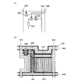
図1を用いて本発明で用いる平行平板型のプラズマCVD装置の処理室(チャンバーとも呼ぶ)の断面図を説明する。図1において、接地されたチャンバー108内には、高周波電源105に接続された第1の電極(上部電極、シャワー電極、高周波電極)121及び接地されている第2の電極(下部電極、接地電極)125が設けられている。第2の電極上に被処理基板127が設置される。
(Embodiment 1)
A cross-sectional view of a processing chamber (also referred to as a chamber) of a parallel plate type plasma CVD apparatus used in the present invention will be described with reference to FIG. In FIG. 1, in a grounded
第1の電極121は、中空構造であって、供給系106aから供給される原料ガスが電極内を通過し、電離されチャンバー内に供給される。ここでは供給系が1系統しか図示していないが、必要に応じて複数のガス供給系を設けることが可能である。
The
また、チャンバーには、排気系107aが設けられ、反応後の排気ガスを排出する。なお、本実施の形態では、電極構造が中空構造(複数のシャワー板が重なりガスを分散する構造、いわゆるシャワーヘッド構造)となっているが、この構造に限られない。供給系が第1の電極と別に設けられていてもよい。また、供給系106a及び排気系107aには、バルブ(106c、107c)が設けられており、供給するガス圧及びチャンバー内の圧力を制御する。
The chamber is provided with an
ヒータ126は、第2の電極125と接して設けられているが、この構造に限られない。また、第1の電極121にヒータ(図示しない)を設けてもよい。また、チャンバーの外壁にヒータを設け、チャンバー内をホットウォール構造としてもよい。
The
また、チャンバーの側面には窓(図示しない)が設けられ、この窓を開閉して基板が収納されているカセット室からロボットアーム等の搬送機構を経由して基板をチャンバー内に移送することができる。 In addition, a window (not shown) is provided on the side surface of the chamber, and the window can be opened and closed to transfer the substrate into the chamber from a cassette chamber in which the substrate is stored via a transport mechanism such as a robot arm. it can.
次に、図1を用いて、成膜方法を述べる。本実施の形態においては、ガラス基板に直接、結晶構造を有する珪素膜の成膜方法を説明する。 Next, a film forming method will be described with reference to FIG. In this embodiment, a method for forming a silicon film having a crystal structure directly on a glass substrate will be described.
原料ガスに珪化物気体(モノシラン、ジシラン、トリシランなど)とフッ素(或いはフッ化ハロゲンガス)を用いる。フッ化ハロゲンガスとしては、ClF、ClF3、BrF、BrF3、IF、IF3などが挙げられる。中でも、モノシランガスとフッ素ガスとの組み合わせが安価なガスの組み合わせであり、量産に適している。ここでは、原料ガスにモノシランガスとフッ素ガスを用いた例で説明を行う。 Silicide gas (monosilane, disilane, trisilane, etc.) and fluorine (or halogen fluoride gas) are used as source gases. Examples of the halogen fluoride gas include ClF, ClF 3 , BrF, BrF 3 , IF, and IF 3 . Among them, the combination of monosilane gas and fluorine gas is an inexpensive gas combination and is suitable for mass production. Here, an example in which monosilane gas and fluorine gas are used as the source gas will be described.
また、他のフッ素系ガスとして、フッ素化モノシラン(SiHmFn:ただし、m+n=4)、四フッ化シラン(SiF4)を用いることもできるが、高価なガスとなる。また、Si−Hの結合(解離)エネルギーは76kcal/molであるのに比べ、Si−Fの結合(解離)エネルギーは142kcal/molと高いため、成膜に必要なエネルギーが高くなり、生産工程における消費エネルギーが増大してしまう。 Further, as other fluorine-based gas, fluorinated monosilane (SiH m F n : where m + n = 4) and tetrafluorosilane (SiF 4 ) can be used, but the gas becomes expensive. Further, since the bond (dissociation) energy of Si—H is 76 kcal / mol, the bond (dissociation) energy of Si—F is as high as 142 kcal / mol. The energy consumption at will increase.
また、成膜条件は、チャンバー内の圧力を1.33×101〜1.33×10³Pa(1×10⁻¹〜1×101torr)、成膜温度を80〜600℃とし、高周波電源の電源周波数を10〜500MHzとする。なお、被処理基板または下地膜として耐熱性の低い材料で形成されている場合には80〜300℃とする。 The film formation conditions were as follows: the pressure in the chamber was 1.33 × 10 1 to 1.33 × 10 3 Pa (1 × 10 −1 to 1 × 10 1 torr), the film formation temperature was 80 to 600 ° C., The power frequency of the high frequency power source is set to 10 to 500 MHz. In the case where the substrate to be processed or the base film is formed of a material having low heat resistance, the temperature is set to 80 to 300 ° C.
図1に示すように、チャンバー内に珪化物気体とフッ素を供給系より導入し、電源のスイッチ122を接続し、電極に高周波電圧を印加し、プラズマ123を発生させる。このプラズマ中で生成される珪化物又はフッ素のイオン、ラジカルなどの化学的に活性な励起種が反応して生成物である結晶構造を有する珪素膜124を形成する。
As shown in FIG. 1, a silicide gas and fluorine are introduced into a chamber from a supply system, a
SiH3ラジカルの堆積による膜成長反応と、Fラジカルによる引き抜き(エッチング)反応とが競争的に起こることにより、Si膜ネットワークの再構成が起こり、結晶構造を含むシリコン膜が形成されると考えられる。 It is considered that the film growth reaction due to the deposition of SiH 3 radicals and the extraction (etching) reaction due to F radicals occur competitively, whereby the Si film network is reconfigured and a silicon film including a crystal structure is formed. .
実際には多種多様な反応が存在するが、ここで、チャンバー内で生じる反応の一例を示す。 There are actually a wide variety of reactions. Here, an example of a reaction that occurs in the chamber is shown.
高周波による気体の分解反応は、数1と数2で表せる。
The gas decomposition reaction due to the high frequency can be expressed by

また、気相中の反応は、数3で表せる。 Further, the reaction in the gas phase can be expressed by Equation 3.
なお、数3で発生するSiH3ラジカルは一般にSi膜成長の主たる化学種と言われている。また、数3では、HFのような腐食性が高いフッ素系ガスが形成されるため、プラズマCVD装置においては、優れた耐腐食性を有する材料で装置内表面を覆うことが望ましい。 The SiH 3 radicals generated in Equation 3 are generally said to be the main chemical species for Si film growth. Further, in Equation 3, since a highly corrosive fluorine-based gas such as HF is formed, in the plasma CVD apparatus, it is desirable to cover the inner surface of the apparatus with a material having excellent corrosion resistance.
また、シリコン膜表面での水素原子引き抜き反応は、数4、数5、数6で表せる。 Further, the hydrogen atom extraction reaction on the silicon film surface can be expressed by the following equations (4), (5), and (6).
また、シリコン膜表面のダングリングボンドへの結合(エッチング反応)は、数7で表せる。
Further, the bond (etching reaction) to the dangling bond on the surface of the silicon film can be expressed by
実際に成膜条件(ガス流量、RFパワー、電極間ギャップ)を振ってそれぞれ成膜を行い、それらの実験結果(膜厚速度、ラマン光学特性(ラマンピーク(Pc、Pa)、ラマン半値幅(Wc、Wa)、積分強度(Ic、Ia)など))を表1に示す。表面にはLPCVD法による酸化珪素膜100nmが予め形成されている被処理基板を用いた。なお、電極面積は380cm2、RF電源周波数は27MHz、上部ヒータ設定温度を65℃、下部ヒータ設定温度を300℃として成膜を行っている。 Actual film formation conditions (gas flow rate, RF power, gap between electrodes) were used for film formation, and the experimental results (film thickness rate, Raman optical characteristics (Raman peak (Pc, Pa), Raman half width ( Table 1 shows Wc, Wa), integrated intensity (Ic, Ia), etc.). A substrate to be processed on which a silicon oxide film 100 nm by LPCVD was previously formed was used on the surface. The film formation is performed with an electrode area of 380 cm 2 , an RF power source frequency of 27 MHz, an upper heater set temperature of 65 ° C., and a lower heater set temperature of 300 ° C.
表1において、ラマン散乱分光法により得られたスペクトルを2つの指数関数型曲線に分離した際に低波数側曲線のピーク(曲線の中心位置)をPa、低波数側曲線のラマン半値幅をWa、低波数側曲線の積分強度をIaとしている。また、高波数側曲線のピークをPc、高波数側曲線のラマン半値幅をWc、高波数側曲線の積分強度をIcとしている。 In Table 1, when the spectrum obtained by the Raman scattering spectroscopy is separated into two exponential curves, the peak of the low wavenumber side curve (the center position of the curve) is Pa, and the Raman half width of the low wavenumber side curve is Wa. The integrated intensity of the low wavenumber side curve is Ia. Further, the peak of the high wave number side curve is Pc, the Raman half width of the high wave number side curve is Wc, and the integrated intensity of the high wave number side curve is Ic.
表1より、300℃の低温でセミアモルファスシリコン膜、或いは微結晶シリコン膜、或いはマイクロクリスタルシリコン膜と呼べる結晶構造を含むシリコン膜が形成されていることが確認できる。得られた結晶構造を含むシリコン膜のPaは、487〜490cm-1、Pcは514〜517cm-1、且つ、Waは42〜47.3cm-1、Wcは9.6〜14.7cm-1にある薄膜である。また、成膜速度(堆積速度)も5nm/min〜20nm/minが得られている。なお、膜厚は10分間の成膜後のものである。 From Table 1, it can be confirmed that a silicon film having a crystal structure called a semi-amorphous silicon film, a microcrystalline silicon film, or a microcrystalline silicon film is formed at a low temperature of 300 ° C. The silicon film including the obtained crystal structure has Pa of 487 to 490 cm −1 , Pc of 514 to 517 cm −1 , Wa of 42 to 47.3 cm −1 , and Wc of 9.6 to 14.7 cm −1. It is a thin film. In addition, the film formation rate (deposition rate) is 5 nm / min to 20 nm / min. The film thickness is after 10 minutes of film formation.
また、モノシランガスは100%、フッ素ガスはHeで希釈された混合ガスを用いており、フッ素含有率は10.1%、不純物(CF4、HF、空気など)のトータル含有率は0.1%未満であり、純度は99.9%である。 Moreover, monosilane gas is 100%, fluorine gas is a mixed gas diluted with He, fluorine content is 10.1%, and total content of impurities (CF 4 , HF, air, etc.) is 0.1%. And the purity is 99.9%.
また、最も結晶化率が高いサンプル(試料9)のラマンスペクトルデータを図2に示す。 In addition, FIG. 2 shows Raman spectrum data of a sample (Sample 9) having the highest crystallization rate.
また、比較例として、成膜条件のうち、圧力を0.3Torrとしてアモルファスシリコン膜が形成された実験結果(比較試料1〜3)を表2に示す。これらの結果から、F2分圧、全圧、RFパワーはいずれも高くなるほど結晶化しやすい傾向が見られる。
As a comparative example, Table 2 shows experimental results (
また、ここではキャリアガスとしてArを用いて3系統のガス供給を行っているが、特にキャリアガスを用いなくともよく、2系統のガス供給のみで成膜を行うこともできる。数の少ないガス系統とすることで成膜条件を調節しやすくすることができる。 In addition, here, three systems of gas supply are performed using Ar as the carrier gas, but it is not particularly necessary to use the carrier gas, and the film formation can be performed only with the two systems of gas supply. By using a few gas systems, it is possible to easily adjust the film forming conditions.
また、水素ガスを供給して3系統のガス供給を行ってもよいし、さらにキャリアガスを供給して4系統のガス供給を行ってもよい。ただし、水素ガスを供給する場合には、水素とフッ素の流量比(H2:F2)を1:10に制御、或いは、この比率よりも下げて水素の流量を少なくすることが好ましい。 Further, hydrogen gas may be supplied to supply three systems of gas, or a carrier gas may be supplied to supply four systems of gas. However, when supplying hydrogen gas, it is preferable to control the flow rate ratio of hydrogen to fluorine (H 2 : F 2 ) to 1:10 or to lower the flow rate to reduce the hydrogen flow rate.
本発明により、安価な大面積の透明絶縁性基板上に、高速の成膜速度で特性の優れた結晶構造を含む半導体膜を低温で直接成膜することができる。 According to the present invention, a semiconductor film including a crystal structure with excellent characteristics can be directly formed at a low temperature on an inexpensive large-area transparent insulating substrate at a high film formation rate.
(実施の形態2)
タクトタイムの向上や、膜厚の均一性向上を図るため、チャンバーの外壁にヒータを設け、チャンバー内をホットウォール構造としたチャンバーを縦方向に重ねて配置したプラズマCVD装置を用いても同様にして成膜を行うことができる。
(Embodiment 2)
In order to improve tact time and improve film thickness uniformity, a plasma CVD apparatus in which a heater is provided on the outer wall of the chamber and a chamber with a hot wall structure inside the chamber is vertically stacked is used. Thus, film formation can be performed.
図3にホットウォール構造としたチャンバーの一例を示す。図3に示すチャンバー208aは、実施の形態1とヒータの設置位置が異なっており、チャンバーの外壁にヒータ226を設け、チャンバー内をホットウォール構造としている。
FIG. 3 shows an example of a chamber having a hot wall structure. The
図3において、208aは接地されたチャンバー、205aは高周波電源、221は原料ガスが電極内を通過する中空構造の第1の電極(上部電極、シャワー電極、高周波電極)、225は接地されている第2の電極(下部電極、接地電極)、106aは供給系、107aは排気系、106c、107cはバルブである。 In FIG. 3, 208a is a grounded chamber, 205a is a high frequency power source, 221 is a hollow first electrode (upper electrode, shower electrode, high frequency electrode) through which the source gas passes through the electrode, and 225 is grounded. The second electrode (lower electrode, ground electrode), 106a is a supply system, 107a is an exhaust system, and 106c and 107c are valves.
なお、チャンバー構成に関する説明は、実施の形態1でも一部述べているので、同じ箇所は同一であるのでここでは詳細な説明を省略する。 In addition, since the description regarding the chamber structure is partly described in the first embodiment, the same portions are the same, and thus detailed description thereof is omitted here.
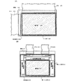
図3に示したチャンバーを縦方向に重ねて配置したプラズマCVD装置の一例の斜視図を図4に示し、上面図を図5に示す。 FIG. 4 shows a perspective view of an example of a plasma CVD apparatus in which the chambers shown in FIG. 3 are arranged in the vertical direction, and FIG. 5 shows a top view thereof.
図4および図5に示す成膜装置は、成膜室及び搬送室を有し、成膜室204a、204bの間に搬送室202bが配置され、搬送室202a、202bが隣接して配置された構造を有する。各成膜室には、縦方向に重ねて配置された10個のチャンバー208a、208bを具備し、各チャンバー208a、208bには、成膜ガスを供給する供給系206a、206b、排気ガスを排気する排気系207a、207b 及び電源205a、205bを具備する。
4 and 5 includes a film formation chamber and a transfer chamber, a transfer chamber 202b is disposed between the film formation chambers 204a and 204b, and the transfer chambers 202a and 202b are disposed adjacent to each other. It has a structure. Each film forming chamber is provided with ten
本装置は、各成膜室204a、204bにおいて、複数のチャンバー208a、208bの全ての供給系は、一つの供給源に接続されていることを特徴とする。同様に、複数のチャンバー208a、208bの全ての排気系は、一つの排気口に接続されていることを特徴とする。本特徴により、本装置では複数のチャンバー208a、208b を縦方向に重ねて配置しているにもかかわらず、供給系206a、206bと排気系207a、207bとを簡単に配置することができる。また、成膜室204a、204bには、各成膜室の圧力を減圧するための排気系(図示しない)が設けられている。チャンバー内の圧力と成膜室内の圧力とを制御することにより、成膜、及びチャンバー内のクリーニングを交互に行うことができ、効率良く成膜を行うことができる。
This apparatus is characterized in that in each of the film forming chambers 204a and 204b, all the supply systems of the plurality of
実施の形態1と同様に、珪化物気体(モノシラン、ジシラン、トリシランなど)とフッ素(或いはフッ化ハロゲンガス)を原料ガスとして導入し、プラズマを発生させて結晶構造を含む半導体膜を被処理基板に直接成膜することができる。 As in the first embodiment, a silicide gas (monosilane, disilane, trisilane, or the like) and fluorine (or halogen fluoride gas) are introduced as source gases, and plasma is generated to form a semiconductor film having a crystal structure. It is possible to form a film directly.
図5において、カセット室201a、201bには所望のサイズのガラス基板、プラスチック基板に代表される樹脂基板等の絶縁表面を有する基板がセットされる。基板の搬送方式として、図示する装置では水平搬送を採用するが、第五世代以降のメータ角の基板を用いる場合、搬送機の占有面積の低減を目的として、基板を縦置きにした縦形搬送を行ってもよい。 In FIG. 5, a substrate having an insulating surface such as a glass substrate of a desired size or a resin substrate typified by a plastic substrate is set in the cassette chambers 201a and 201b. As the substrate transfer method, horizontal transfer is adopted in the equipment shown in the figure, but when using a meter angle substrate of the fifth generation or later, vertical transfer with the substrate placed vertically is used for the purpose of reducing the area occupied by the transfer machine. You may go.
搬送室202a、202bの各々には、搬送機構(ロボットアーム)203a、203bが具備されている。搬送機構により、カセット室201a、201bにセットされた基板が各成膜室204a、204bに搬送される。そして、成膜室204a、204bのチャンバー208a、208bにおいて、搬送された基板の被処理面に対して所定の処理が行われる。また、図5において、搬送室が複数設けられているが、これは一つでもよい。
Each of the transfer chambers 202a and 202b is provided with transfer mechanisms (robot arms) 203a and 203b. The substrate set in the cassette chambers 201a and 201b is transferred to the film forming chambers 204a and 204b by the transfer mechanism. Then, in the
ここでは、数十枚の基板を一度に処理するバッチ式装置を例示したが、基板を一枚ずつ処理する枚葉式装置に本発明を適用することもできる。 Here, a batch type apparatus that processes several tens of substrates at a time is illustrated, but the present invention can also be applied to a single wafer type apparatus that processes substrates one by one.
図4に示すように、複数のチャンバーを有する成膜装置で成膜することにより、同時に多数の基板に同条件で形成される膜を形成することができる。このため、基板間のバラツキを低減することが可能となり、歩留まりを向上させることができる。また、スループットを向上することもできる。 As shown in FIG. 4, by forming a film with a film forming apparatus having a plurality of chambers, films formed under the same conditions on a large number of substrates can be formed at the same time. For this reason, it becomes possible to reduce the variation between substrates, and to improve a yield. In addition, throughput can be improved.
以上の構成でなる本発明について、以下に示す実施例でもってさらに詳細な説明を行うこととする。 The present invention having the above-described configuration will be described in more detail with the following examples.
本実施例では、逆スタガ型TFTをスイッチング素子とするアクティブマトリクス型液晶表示装置の作製方法を示す。なお、図6は作製工程の断面を示している。 In this embodiment, a method for manufacturing an active matrix liquid crystal display device using an inverted staggered TFT as a switching element will be described. FIG. 6 shows a cross section of the manufacturing process.
まず、基板10上に後に形成する液滴吐出法による材料層と密着性を向上させるための下地膜11を形成する。下地膜11は、極薄く形成すれば良いので、必ずしも層構造を持っていなくても良く、下地前処理とみなすこともできる。スプレーによって光触媒物質(酸化チタン(TiOX)、チタン酸ストロンチウム(SrTiO3)、セレン化カドミウム(CdSe)、タンタル酸カリウム(KTaO3)、硫化カドミウム(CdS)、酸化ジルコニウム(ZrO2)、酸化ニオブ(Nb2O5)、酸化亜鉛(ZnO)、酸化鉄(Fe2O3)、酸化タングステン(WO3))を全面に滴下、またはインクジェット法やゾルゲル法を用いて有機材料(ポリイミド、アクリル、或いは、シリコン(Si)と酸素(O)との結合で骨格構造が構成され、置換基に水素、フッ素、アルキル基、または芳香族炭化水素のうち少なくとも1種を有する材料を用いた塗布絶縁膜)を選択的に形成してもよい。
First, a base layer 11 is formed on the
光触媒物質は、光触媒機能を有する物質を指し、紫外光領域の光(波長400nm以下、好ましくは380nm以下)を照射し、光触媒活性を生じさせるものである。光触媒物質上に、インクジェット法により、溶媒に混入された導電体を吐出すると、微細な描画を行うことができる。 The photocatalytic substance refers to a substance having a photocatalytic function, and emits light in the ultraviolet region (wavelength of 400 nm or less, preferably 380 nm or less) to cause photocatalytic activity. When a conductor mixed in a solvent is discharged onto the photocatalyst material by an ink jet method, fine drawing can be performed.
例えば、TiOXに光照射する前、親油性はあるが、親水性はない、つまり撥水性の状態にある。光照射を行うことにより、光触媒活性が起こり、親水性にかわり、逆に親油性がない状態、つまり撥油性となる。なお光照射時間により、親水性と親油性を共に有する状態にもなりうる。 For example, before TiO x is irradiated with light, it is lipophilic but not hydrophilic, that is, it is in a water-repellent state. By performing light irradiation, photocatalytic activity occurs, and instead of hydrophilicity, there is no lipophilicity, that is, oil repellency. Depending on the light irradiation time, both hydrophilicity and lipophilicity can be achieved.
なお、親水性とは、水に濡れやすい状態を指し、接触角が30度以下、特に接触角が5度以下を超親水性という。一方撥水性とは、水に濡れにくい状態を指し、接触角が90度以上のものを指す。同様に親油性とは、油に濡れやすい状態を指し、撥油性とは油に濡れにくい状態を指す。なお接触角とは、滴下したドットのふちにおける、形成面と液滴の接線がなす角度のことを指す。 In addition, hydrophilicity refers to the state which is easy to get wet with water, and a contact angle of 30 degrees or less, especially a contact angle of 5 degrees or less is called super hydrophilicity. On the other hand, water repellency refers to a state in which it is difficult to wet with water, and refers to a contact angle of 90 degrees or more. Similarly, “lipophilic” refers to a state that is easily wetted with oil, and “oil repellency” refers to a state that is difficult to wet with oil. The contact angle refers to an angle formed by the tangent line between the formation surface and the droplet at the edge of the dropped dot.
すなわち、光照射を行った領域(以下、照射領域と表記する)は、親水性領域、又は超親水性(合わせて単に親水性と表記する)となる。このとき、照射領域の幅を所望の配線幅となるように光照射を行う。その後、インクジェット法により、照射領域上から又は照射領域にむかって、水系の溶媒に導電体が混入したドットを吐出する。すると、単にインクジェット法により吐出されたドットの径より小さな、つまり幅の狭い配線を形成することができる。これは所望の配線幅となるように照射領域が形成されるため、吐出されたドットが形成表面で広がることを抑制できるからである。更に、ドットが多少ずれて吐出された場合であっても、照射領域に沿って配線を形成することができ、配線形成の正確な位置制御が可能となる。 That is, the region irradiated with light (hereinafter referred to as an irradiation region) becomes a hydrophilic region or super hydrophilicity (hereinafter simply referred to as hydrophilicity). At this time, light irradiation is performed so that the width of the irradiation region becomes a desired wiring width. Thereafter, dots in which a conductor is mixed in an aqueous solvent are ejected from the irradiation region toward the irradiation region by an inkjet method. Then, it is possible to form a wiring that is smaller than the diameter of the dots ejected simply by the ink jet method, that is, has a narrow width. This is because the irradiation region is formed so as to have a desired wiring width, so that it is possible to prevent the discharged dots from spreading on the formation surface. Furthermore, even when dots are ejected with a slight shift, wiring can be formed along the irradiation region, and accurate position control of wiring formation is possible.
なお、水系の溶媒を用いる場合、インクジェットのノズルからスムーズに吐出できるように界面活性剤を添加すると好ましい。 When an aqueous solvent is used, it is preferable to add a surfactant so that it can be smoothly discharged from an inkjet nozzle.
また、油(アルコール)系の溶媒に混入された導電体を吐出する場合、光照射が行われない領域(以下、非照射領域と表記する)に導電体を吐出し、非照射領域上から又は非照射領域にむかってドットを吐出することにより、同様に配線を形成することができる。すなわち、配線を形成したい領域の両端、つまり配線を形成したい領域を囲むような周囲に光照射を行い、照射領域を形成すればよい。このとき照射領域は撥油性を有するため、油(アルコール)系の溶媒に混入された導電体を有するドットは、選択的に非照射領域に形成されるからである。すなわち、非照射領域の幅を所望の配線幅となるように光照射を行う。 Further, when discharging a conductor mixed in an oil (alcohol) -based solvent, the conductor is discharged to a region where light irradiation is not performed (hereinafter referred to as a non-irradiation region), or from above the non-irradiation region or By ejecting dots toward the non-irradiated area, wiring can be formed in the same manner. That is, light irradiation may be performed by forming light irradiation on both ends of a region where wiring is to be formed, that is, surroundings surrounding a region where wiring is to be formed. At this time, since the irradiated region has oil repellency, dots having a conductor mixed in an oil (alcohol) -based solvent are selectively formed in the non-irradiated region. That is, light irradiation is performed so that the width of the non-irradiation region becomes a desired wiring width.
なお、油(アルコール)系の溶媒は、非極性溶剤又は低極性溶剤を用いることができる。例えば、テルピネオール、ミネラルスピリット、キシレン、トルエン、エチルベンゼン、メシチレン、ヘキサン、ヘプタン、オクタン、デカン、ドデカン、シクロヘキサン、又はシクロオクタンを用いることができる。 As the oil (alcohol) -based solvent, a nonpolar solvent or a low polarity solvent can be used. For example, terpineol, mineral spirit, xylene, toluene, ethylbenzene, mesitylene, hexane, heptane, octane, decane, dodecane, cyclohexane, or cyclooctane can be used.
更に光触媒物質へ遷移金属(Pd、Pt、Cr、Ni、V、Mn、Fe、Ce、Mo、W等)をドーピングすることにより、光触媒活性を向上させたり、可視光領域(波長400nm〜800nm)の光により光触媒活性を起こすことができる。遷移金属は、広いバンドギャップを持つ活性な光触媒の禁制帯内に新しい準位を形成し、可視光領域まで光の吸収範囲を拡大しうるからである。例えば、CrやNiのアクセプター型、VやMnのドナー型、Fe等の両性型、その他Ce、Mo、W等をドーピングすることができる。このように光の波長は光触媒物質によって決定することができるため、光照射とは光触媒物質の光触媒活性化させる波長の光を照射することを指す。
Furthermore, the photocatalytic substance can be doped with transition metals (Pd, Pt, Cr, Ni, V, Mn, Fe, Ce, Mo, W, etc.) to improve the photocatalytic activity or visible light region (
また、光触媒物質を真空中又は水素環流中で加熱し還元させると、結晶中に酸素欠陥が発生する。このように遷移元素をドーピングしなくても、酸素欠陥は電子ドナーと同等の役割を果たす。特に、ゾルゲル法により形成する場合、酸素欠陥が最初から存在するため、還元しなくともよい。またN2等のガスをドープすることにより、酸素欠陥を形成することができる。 In addition, when the photocatalytic substance is heated and reduced in a vacuum or hydrogen reflux, oxygen defects are generated in the crystal. Thus, oxygen defects play the same role as electron donors even without doping with a transition element. In particular, in the case of forming by the sol-gel method, oxygen defects are present from the beginning, so that reduction is not necessary. Further, oxygen defects can be formed by doping a gas such as N 2 .
また、ここでは基板上に導電性材料を吐出する場合に密着性を良くする下地前処理を行う例を示したが、特に限定されず、材料層(例えば、有機層、無機層、金属層)、或いは、吐出した導電性層の上にさらに液滴吐出法で材料層(例えば、有機層、無機層、金属層)を形成する場合において、材料層と材料層との密着性向上のためのTiOX成膜処理を行っても良い。つまり、液滴吐出法で導電性材料を吐出して描画する場合、その導電性材料層の上下界面で下地前処理を挟み、その密着性を良くすることが望ましい。 In addition, here, an example of performing the base pretreatment for improving adhesion when discharging a conductive material onto a substrate is shown, but there is no particular limitation, and a material layer (for example, an organic layer, an inorganic layer, a metal layer) Alternatively, in the case where a material layer (for example, an organic layer, an inorganic layer, or a metal layer) is further formed on the discharged conductive layer by a droplet discharge method, for improving the adhesion between the material layer and the material layer. A TiO x film forming process may be performed. That is, when drawing is performed by discharging a conductive material by a droplet discharge method, it is desirable that the base pretreatment is sandwiched between the upper and lower interfaces of the conductive material layer to improve the adhesion.
なお、基板10は、バリウムホウケイ酸ガラス、アルミノホウケイ酸ガラス若しくはアルミノシリケートガラスなど、フュージョン法やフロート法で作製される無アルカリガラス基板の他、本作製工程の処理温度に耐えうる耐熱性を有するプラスチック基板等を用いることができる。また、反射型の液晶表示装置とする場合、単結晶シリコンなどの半導体基板、ステンレスなどの金属基板、またはセラミック基板の表面に絶縁層を設けた基板を適用しても良い。
Note that the
次いで、液滴吐出法、代表的にはインクジェット法により滴下した後、酸素雰囲気で焼成を行い、ゲート電極またはゲート配線となる金属配線12を形成する。また、同様に端子部に伸びる配線40も形成する。なお、ここでは図示しないが、保持容量を形成するための容量電極または容量配線をも形成する。
Next, after dropping by a droplet discharge method, typically an ink jet method, baking is performed in an oxygen atmosphere to form a
これらの配線材料としては、金(Au)、銀(Ag)、銅(Cu)、白金(Pt)、パラジウム(Pd)、タングステン(W)、ニッケル(Ni)、タンタル(Ta)、ビスマス(Bi)、鉛(Pb)、インジウム(In)、錫(Sn)、亜鉛(Zn)、チタン(Ti)、若しくはアルミニウム(Al)、これらからなる合金、これらの分散性ナノ粒子、又はハロゲン化銀の微粒子を用いる。特に、ゲート配線は、低抵抗化することが好ましいので、比抵抗値を考慮して、金、銀、銅のいずれかの材料を溶媒に溶解又は分散させたものを用いることが好適であり、より好適には、低抵抗な銀、銅を用いるとよい。但し、銀、銅を用いる場合には、不純物拡散防止対策のため、合わせてバリア膜を設けるとよい。溶媒は、酢酸ブチル等のエステル類、イソプロピルアルコール等のアルコール類、アセトン等の有機溶剤等に相当する。表面張力と粘度は、溶媒の濃度を調整したり、界面活性剤等を加えたりして適宜調整する。 These wiring materials include gold (Au), silver (Ag), copper (Cu), platinum (Pt), palladium (Pd), tungsten (W), nickel (Ni), tantalum (Ta), bismuth (Bi). ), Lead (Pb), indium (In), tin (Sn), zinc (Zn), titanium (Ti), or aluminum (Al), alloys thereof, dispersible nanoparticles thereof, or silver halide Use fine particles. In particular, since it is preferable to reduce the resistance of the gate wiring, it is preferable to use a material in which any one of gold, silver, and copper is dissolved or dispersed in consideration of the specific resistance value. More preferably, low resistance silver or copper is used. However, when silver or copper is used, it is preferable to provide a barrier film together to prevent impurity diffusion. The solvent corresponds to esters such as butyl acetate, alcohols such as isopropyl alcohol, organic solvents such as acetone, and the like. The surface tension and the viscosity are appropriately adjusted by adjusting the concentration of the solvent or adding a surfactant or the like.
液滴吐出法において用いるノズルの径は、0.02〜100μm(好適には30μm以下)に設定し、該ノズルから吐出される組成物の吐出量は0.001pl〜100pl(好適には10pl以下)に設定することが好ましい。液滴吐出法には、オンデマンド型とコンティニュアス型の2つの方式があるが、どちらの方式を用いてもよい。さらに液滴吐出法において用いるノズルには、圧電体の電圧印加により変形する性質を利用した圧電方式、ノズル内に設けられたヒータにより組成物を沸騰させ該組成物を吐出する加熱方式があるが、そのどちらの方式を用いてもよい。被処理物とノズルの吐出口との距離は、所望の箇所に滴下するために、出来る限り近づけておくことが好ましく、好適には0.1〜3mm(好適には1mm以下)程度に設定する。ノズルと被処理物は、その相対的な距離を保ちながら、ノズル及び被処理物の一方が移動して、所望のパターンを描画する。また、組成物を吐出する前に、被処理物の表面にプラズマ処理を施してもよい。これは、プラズマ処理を施すと、被処理物の表面が親水性になったり、疎液性になったりすることを活用するためである。例えば、純水に対しては親水性になり、アルコールを溶媒したペーストに対しては疎液性になる。 The diameter of the nozzle used in the droplet discharge method is set to 0.02 to 100 μm (preferably 30 μm or less), and the discharge amount of the composition discharged from the nozzle is 0.001 pl to 100 pl (preferably 10 pl or less). ) Is preferable. There are two types of droplet discharge methods, an on-demand type and a continuous type, and either method may be used. Furthermore, the nozzle used in the droplet discharge method includes a piezoelectric method that utilizes the property of being deformed by voltage application of a piezoelectric body, and a heating method that discharges the composition by boiling the composition with a heater provided in the nozzle. Either of these methods may be used. The distance between the object to be processed and the nozzle outlet is preferably as close as possible in order to drop it at a desired location, and is preferably set to about 0.1 to 3 mm (preferably 1 mm or less). . While maintaining the relative distance between the nozzle and the object to be processed, one of the nozzle and the object to be processed moves to draw a desired pattern. In addition, plasma treatment may be performed on the surface of the object to be processed before the composition is discharged. This is to take advantage of the fact that the surface of the workpiece becomes hydrophilic or lyophobic when the plasma treatment is performed. For example, it becomes hydrophilic with respect to pure water and becomes lyophobic with respect to a paste using an alcohol as a solvent.
組成物を吐出する工程は、減圧下で行っても良い。これは、組成物を吐出して被処理物に着弾するまでの間に、該組成物の溶媒が揮発し、後の乾燥と焼成の工程を省略又は短くすることができるためである。組成物の吐出後は、常圧下又は減圧下で、レーザ光の照射や瞬間熱アニール、加熱炉等により、乾燥と焼成の一方又は両方の工程を行う。乾燥と焼成の工程は、両工程とも加熱処理の工程であるが、例えば、乾燥は100度で3分間、焼成は200〜350度で15分間〜120分間で行うもので、その目的、温度と時間が異なるものである。乾燥と焼成の工程を良好に行うためには、基板を加熱しておいてもよく、そのときの温度は、基板等の材質に依存するが、100〜800度(好ましくは200〜350度)とする。本工程により、組成物中の溶媒の揮発又は化学的に分散剤を除去し、周囲の樹脂が硬化収縮することで、融合と融着を加速する。雰囲気は、酸素雰囲気、窒素雰囲気又は空気で行う。但し、金属元素を分解又は分散している溶媒が除去されやすい酸素雰囲気下で行うことが好適である。 The step of discharging the composition may be performed under reduced pressure. This is because the solvent of the composition volatilizes before the composition is discharged and landed on the object to be processed, and the subsequent drying and firing steps can be omitted or shortened. After discharge of the composition, one or both of drying and baking steps are performed under normal pressure or reduced pressure by laser light irradiation, rapid thermal annealing, a heating furnace, or the like. The drying and firing steps are both heat treatment steps. For example, the drying is performed at 100 degrees for 3 minutes, and the firing is performed at 200 to 350 degrees for 15 minutes to 120 minutes. Time is different. In order to satisfactorily perform the drying and firing steps, the substrate may be heated, and the temperature at that time depends on the material of the substrate or the like, but is 100 to 800 degrees (preferably 200 to 350 degrees). And By this step, the solvent in the composition is volatilized or the dispersant is chemically removed, and the surrounding resin is cured and shrunk to accelerate fusion and fusion. The atmosphere is an oxygen atmosphere, a nitrogen atmosphere or air. However, it is preferable to perform in an oxygen atmosphere in which the solvent in which the metal element is decomposed or dispersed is easily removed.
上記下地膜の形成または下地前処理を行うことによって、後に形成する液滴吐出法での金属層の密着性が大幅に向上され、希フッ酸(1/100希釈)に浸けても1分以上耐えることができ、テープ剥がし試験でも十分な密着性が確保されている。 By performing the above-mentioned base film formation or base pretreatment, the adhesion of the metal layer in the droplet discharge method to be formed later is greatly improved. Even if immersed in dilute hydrofluoric acid (1/100 dilution), it takes 1 minute or more. It can withstand, and sufficient adhesion is secured even in a tape peeling test.
次いで、プラズマCVD法やスパッタリング法を用いて、ゲート絶縁膜13を単層又は積層構造で形成する。望ましくは、ゲート絶縁膜13として、窒化珪素からなる絶縁体層、酸化珪素からなる絶縁体層、窒化珪素からなる絶縁体層の3層の積層とする。ただし、ゲート絶縁膜13の成膜温度で金属配線12がダメージを受けないようにする。なお、ゲートリーク電流が少ない緻密な絶縁膜を低い成膜温度で形成するには、アルゴンなどの希ガス元素を反応ガスに含ませ、形成される絶縁膜中に混入させると良い。
Next, the
次いで、半導体膜14aを形成する。本実施例では、SiH4とF2を原料ガスに用いたPCVD法により得られるセミアモルファス半導体膜を形成する。高速の成膜速度でセミアモルファス半導体膜を低温で直接成膜することができる。実施の形態1に示す成膜方法に従って、金属配線12の耐熱温度を超えることなく、金属配線12の上方に特性の優れた結晶構造を含む半導体膜を成膜する。なお、セミアモルファスシリコン膜は、下地との界面により結晶性を持たせることができるため好ましい。
Next, the
次いで、絶縁体層16をプラズマCVD法やスパッタリング法で形成する。なお、パターニングは、液滴吐出法で形成されたマスクを用いたエッチング、またはフォトリソグラフィ技術を用いればよい。この絶縁体層16は、ゲート電極層と相対して半導体層上に残存させて、チャネル保護層とするものである。また、絶縁体層16としては、界面の清浄性を確保して、有機物や金属物、水蒸気などの不純物で半導体層が汚染されることを防ぐ効果を得るために、緻密な膜で形成することが好ましい。グロー放電分解法においても、珪化物気体をアルゴンなどの珪化物気体で100倍〜500倍に希釈して形成された窒化珪素膜は、100℃以下の成膜温度でも緻密な膜を形成可能であり好ましい。
Next, the
次いで、絶縁体層16を覆うマスク15を液滴吐出法で形成する。(図6(A))マスク15は、エポキシ樹脂、アクリル樹脂、フェノール樹脂、ノボラック樹脂、アクリル樹脂、メラミン樹脂、ウレタン樹脂等の樹脂材料を用いる。また、ベンゾシクロブテン、パリレン、フレア、透過性を有するポリイミドなどの有機材料、シロキサン系ポリマー等の重合によってできた化合物材料、水溶性ホモポリマーと水溶性共重合体を含む組成物材料等を用いて液滴吐出法で形成する。或いは、感光剤を含む市販のレジスト材料を用いてもよく、例えば、代表的なポジ型レジストである、ノボラック樹脂と感光剤であるナフトキノンジアジド化合物、ネガ型レジストであるベース樹脂、ジフェニルシランジオール及び酸発生剤などを用いてもよい。いずれの材料を用いるとしても、その表面張力と粘度は、溶媒の濃度を調整したり、界面活性剤等を加えたりして適宜調整する。
Next, a
次いで、マスク15で覆われた領域以外の半導体膜14aをドライエッチングまたはウェットエッチングにより除去して活性層となる半導体層14bを形成する。
Next, the
次いで、マスク15を除去した後、n型の半導体膜17を全面に形成する。なおn型の半導体膜を設ける場合、半導体膜と電極とのコンタクト抵抗が低くなり好ましいが、必要に応じて設ければよい。n型の半導体膜17は、シランガスとフォスフィンガスを用いたPCVD法で形成すれば良く、アモルファス半導体膜、或いはセミアモルファス半導体膜で形成することができる。
Next, after removing the
次いで、液滴吐出法により導電性材料(Ag(銀)、Au(金)、Cu(銅)、W(タングステン)、Al(アルミニウム)等)を含む組成物を選択的に吐出して、ソース配線またはドレイン配線18a、18bを形成する。なお、同様に、端子部において接続配線41も形成する。(図6(B))
Next, a composition containing a conductive material (Ag (silver), Au (gold), Cu (copper), W (tungsten), Al (aluminum), etc.)) is selectively discharged by a droplet discharge method, and the source Wiring or
次いで、ソース配線またはドレイン配線18a、18bをマスクとして自己整合的にn型の半導体膜17をエッチングして、ソース領域またはドレイン領域19a、19bを形成する。この段階でチャネルストップ型のTFT30が完成する。絶縁体層16は、n型の半導体膜のエッチングストッパーとして機能させる。
Next, the n-
次いで、シャドーマスクを用いて端子部以外をレジストなどの樹脂で覆い、端子部においては、接続配線41をマスクとしたゲート絶縁膜13のエッチングを行って配線40の一部を露呈させる。また、シャドーマスクに代えてスクリーン印刷法によりレジストマスクを形成してエッチングマスクとしてもよい。なお、端子部以外をレジストで覆うことなくゲート絶縁膜13のエッチングを行ってもよいが、画素部において、ソース配線またはドレイン配線18a、18bと重ならない領域のゲート絶縁膜がエッチングされてしまう点と、絶縁体層16がエッチングされて半導体層が露呈してしまう恐れがある点で問題がある。
Next, a portion other than the terminal portion is covered with a resin such as a resist using a shadow mask, and in the terminal portion, the
次いで、端子部に伸びる配線40と接続配線41との接続を行うための導電物42を形成する。導電物42は印刷法または液滴吐出法により形成すればよい。液滴吐出法を用いる場合、導電性材料(Ag(銀)、Au(金)、Cu(銅)、W(タングステン)、Al(アルミニウム)等)を含む組成物を選択的に吐出して導電物42を形成する。
Next, a
次いで、ソース配線またはドレイン配線18a上の一部に導電性部材からなる凸状部(ピラー)20を形成する。凸状部(ピラー)20は、導電性材料(Ag(銀)、Au(金)、Cu(銅)、W(タングステン)、Al(アルミニウム)等)を含む組成物の吐出と焼成を繰り返すことによって積み重ねる。また、同様に接続配線41上にも凸状部(ピラー)43を形成する。或いは、凸状部(ピラー)20は、スパッタ法により得た金属膜をパターニングすることで形成してもよく、この場合、凸状部(ピラー)は柱状となる。
Next, a convex portion (pillar) 20 made of a conductive member is formed on a part of the source wiring or
次いで、塗布法による平坦な層間絶縁膜21を形成する。(図6(C))塗布法による平坦な層間絶縁膜とは、液状の組成物を塗布して形成する層間絶縁膜を指す。塗布法による平坦な層間絶縁膜としては、アクリル、ポリイミドなどの有機樹脂、有機溶媒中に溶かされた絶縁膜材料を塗布した後熱処理により被膜を形成する所謂、塗布珪素酸化膜(Spin on Glass、以下「SOG」ともいう。)、シロキサンポリマーなどの焼成によりシロキサン結合を形成する材料などが挙げられる。また、層間絶縁膜21は、塗布法に限定されず、気相成長法やスパッタリング法により形成された酸化珪素膜などの無機絶縁膜も用いることができる。また、保護膜として窒化珪素膜をPCVD法やスパッタ法で形成した後、塗布法による平坦な絶縁膜を積層してもよい。
Next, a flat
また、液滴吐出法により層間絶縁膜21を形成してもよい。また、凸状部(ピラー)20、43を本焼成する前に層間絶縁膜21を液滴吐出法により形成し、同時に本焼成してもよい。
Further, the
なお、塗布法や液滴吐出法による平坦な層間絶縁膜21を形成する際、スキージではなく、エアナイフで表面におけるミクロの凹凸を平坦化させた後、本焼成を行うことが好ましい。
When the flat
次いで、全面エッチバックにより凸状部(ピラー)20、43上の層間絶縁膜を除去して凸状部(ピラー)20、43を露出させる。また、他の方法としては、化学的機械研磨(CMP)により、層間絶縁膜を研削し、その後、層間絶縁膜を全面エッチバックすることにより、凸状部(ピラー)20、43を露出させることができる。 Next, the interlayer insulating film on the convex portions (pillars) 20 and 43 is removed by etching back the entire surface to expose the convex portions (pillars) 20 and 43. As another method, the convex portions (pillars) 20 and 43 are exposed by grinding the interlayer insulating film by chemical mechanical polishing (CMP) and then etching back the entire surface of the interlayer insulating film. Can do.
次いで、層間絶縁膜22上に凸状部(ピラー)20と接する画素電極23を形成する。(図6(D))なお、同様に凸状部(ピラー)43と接する端子電極44も形成する。透過型の液晶表示パネルを作製する場合には、液滴吐出法または印刷法によりインジウム錫酸化物(ITO)、酸化珪素を含むインジウム錫酸化物(ITSO)、酸化亜鉛(ZnO)、酸化スズ(SnO2)などを含む組成物からなる所定のパターンを形成し、焼成して画素電極23および端子電極44を形成しても良い。また、反射型の液晶表示パネルを作製する場合には、画素電極23および端子電極44を液滴吐出法によりAg(銀)、Au(金)、Cu(銅)、W(タングステン)、Al(アルミニウム)等の金属の粒子を主成分とした組成物を用いて形成することができる。他の方法としては、スパッタリング法により透明導電膜、若しくは光反射性の導電膜を形成して、液滴吐出法によりマスクパターンを形成し、エッチングを組み合わせて画素電極を形成しても良い。なお、エッチバックやCMPにより層間絶縁膜22の表面は平坦化されており、平坦な画素電極23を形成することができる。
Next, a
なお、図7に画素部の一部を拡大した上面図を示す。また、図7は画素電極の形成途中を示しており、左側の画素においては画素電極が形成されているが、右側の画素においては画素電極を形成していない状態を示している。図7において、実線A−A’で切断した図が、図6(D)の画素部の断面と対応しており、図6(D)と対応する箇所には同じ符号を用いている。また、容量配線31が設けてあり、保持容量は、ゲート絶縁膜を誘電体とし、画素電極23と、該画素電極と重なる容量配線31とで形成されている。
Note that FIG. 7 shows an enlarged top view of a part of the pixel portion. FIG. 7 shows a state where the pixel electrode is being formed. In the left pixel, the pixel electrode is formed, but in the right pixel, the pixel electrode is not formed. In FIG. 7, a diagram cut along a solid line A-A ′ corresponds to the cross section of the pixel portion in FIG. 6D, and the same reference numerals are used for portions corresponding to FIG. 6D. In addition, the
以上の工程により、基板10上にボトムゲート型(逆スタガ型ともいう。)のTFTおよび画素電極が形成された液晶表示パネル用のTFT基板が完成する。
Through the above steps, a TFT substrate for a liquid crystal display panel in which a bottom gate type (also referred to as an inverted stagger type) TFT and a pixel electrode are formed on the
次いで、画素電極23を覆うように、配向膜24aを形成する。なお、配向膜24aは、液滴吐出法やスクリーン印刷法やオフセット印刷法を用いればよい。その後、配向膜24aの表面にラビング処理を行う。
Next, an alignment film 24 a is formed so as to cover the
そして、対向基板25には、着色層26a、遮光層(ブラックマトリクス)26b、及びオーバーコート層27からなるカラーフィルタを設け、さらに透明電極からなる対向電極と、その上に配向膜24bを形成する。そして、閉パターンであるシール材(図示しない)を液滴吐出法により画素部と重なる領域を囲むように形成する。ここでは液晶を滴下するため、閉パターンのシール材を描画する例を示すが、開口部を有するシールパターンを設け、TFT基板を貼りあわせた後に毛細管現象を用いて液晶を注入するディップ式(汲み上げ式)を用いてもよい。
The
次いで、気泡が入らないように減圧下で液晶の滴下を行い、両方の基板を貼り合わせる。閉ループのシールパターン内に液晶を1回若しくは複数回滴下する。液晶の配向モードとしては、液晶分子の配列が光の入射から出射に向かって90°ツイスト配向したTNモードを用いる場合が多い。TNモードの液晶表示装置を作製する場合には、基板のラビング方向が直交するように貼り合わせる。 Next, liquid crystal is dropped under reduced pressure so that bubbles do not enter, and both substrates are bonded together. The liquid crystal is dropped once or a plurality of times in the closed loop seal pattern. As the alignment mode of the liquid crystal, a TN mode in which the alignment of liquid crystal molecules is twisted by 90 ° from the incident light to the emitted light is often used. When a TN mode liquid crystal display device is manufactured, the substrates are bonded so that the rubbing directions of the substrates are orthogonal.
なお、一対の基板間隔は、球状のスペーサを散布したり、樹脂からなる柱状のスペーサを形成したり、シール材にフィラーを含ませることによって維持すればよい。上記柱状のスペーサは、アクリル、ポリイミド、ポリイミドアミド、エポキシの少なくとも1つを主成分とする有機樹脂材料、もしくは酸化珪素、窒化珪素、酸化窒化珪素のいずれか一種の材料、或いはこれらの積層膜からなる無機材料であることを特徴としている。 Note that the distance between the pair of substrates may be maintained by spraying spherical spacers, forming columnar spacers made of resin, or including a filler in the sealing material. The columnar spacer is made of an organic resin material mainly containing at least one of acrylic, polyimide, polyimide amide, and epoxy, or any one of silicon oxide, silicon nitride, and silicon oxynitride, or a laminated film thereof. It is characterized by being an inorganic material.
次いで、必要でない基板の分断を行う。多面取りの場合、それぞれのパネルを分断する。また、1面取りの場合、予めカットされている対向基板を貼り合わせることによって、分断工程を省略することもできる。 Next, the unnecessary substrate is divided. In case of multi-chamfering, each panel is divided. In the case of one-sided chamfering, the dividing step can be omitted by attaching a counter substrate that has been cut in advance.
そして、異方性導電体層45を介し、公知の技術を用いてFPC46を貼りつける。以上の工程で液晶モジュールが完成する。(図6(E))また、必要があれば光学フィルムを貼り付ける。透過型の液晶表示装置とする場合、偏光板は、アクティブマトリクス基板と対向基板の両方に貼り付ける。
Then, the
以上示したように、本実施例では、活性層となるセミアモルファスシリコン膜をプラズマCVD法で成膜温度300℃、成膜速度5nm/min〜20nm/minを実現し、低温、且つ、短時間で成膜することによりコストの低減、および工程時間の短縮を図ることができる。また、凸状部(ピラー)43を用いてフォトマスクを利用した光露光工程を削減することにより、工程を単純化するとともに、工程時間を短縮することができる。また、液滴吐出法を用いて基板上に直接的に各種のパターンを形成することにより、1辺が1000mmを超える第5世代以降のガラス基板を用いても、容易に液晶表示パネルを製造することができる。 As described above, in this embodiment, a semi-amorphous silicon film serving as an active layer is formed by a plasma CVD method at a film forming temperature of 300 ° C. and a film forming speed of 5 nm / min to 20 nm / min. By forming a film with this, the cost can be reduced and the process time can be shortened. Moreover, by reducing the light exposure process using a photomask using the convex part (pillar) 43, a process can be simplified and process time can be shortened. In addition, by forming various patterns directly on the substrate using the droplet discharge method, a liquid crystal display panel can be easily manufactured even if a glass substrate of the fifth generation or more with one side exceeding 1000 mm is used. be able to.
走査方向に対して3列とし、大型基板に対応させた液滴吐出装置(代表的にはインクジェット装置)の一例を図8に示す。図8において、1500は大面積基板、1504は撮像手段、1507はステージ、1511はマーカー、1503は1つのパネルが形成される領域を示している。1つのパネルの幅と同じ幅のヘッド1505a、1505b、1505cを備え、このヘッドをジグザグまたは往復させたりして適宜、材料層のパターンを形成する。
FIG. 8 shows an example of a droplet discharge device (typically an ink jet device) corresponding to a large substrate with three rows in the scanning direction. In FIG. 8, 1500 is a large area substrate, 1504 is an imaging means, 1507 is a stage, 1511 is a marker, and 1503 is a region where one panel is formed. The
個々のヘッド1505a、1505b、1505cは制御手段(図示しない)に接続され、それがコンピュータ(図示しない)で制御することにより予めプログラミングされたパターンを描画することができる。描画するタイミングは、例えば、大面積基板1500上に形成されたマーカー1511を基準に行えば良い。或いは、大面積基板1500の縁を基準にして基準点を確定させても良い。これをCCDなどの撮像手段1504で検出し、画像処理手段(図示しない)にてデジタル信号に変換したものをコンピュータで認識して制御信号を発生させて制御手段に送る。勿論、大面積基板1500上に形成されるべきパターンの情報は記憶媒体(図示しない)に格納されたものであり、この情報を基にして制御手段に制御信号を送り、個々のヘッド1505a、1505b、1505cを個別に制御することができる。
The
図8において、走査方向に対して3列としたヘッド1505a、1505b、1505cはそれぞれ異なる材料層を形成することを可能としてもよいし、同一材料を吐出してもよい。3つのヘッドで同一材料を吐出して層間絶縁膜をパターン形成する場合にはスループットが向上する。
In FIG. 8,
なお、図8に示す装置は、ヘッド部を固定し、大面積基板1500を移動させて走査させることも、大面積基板1500を固定し、基板1500を固定させて走査させることも可能である。
Note that the apparatus shown in FIG. 8 can scan with the head portion fixed and the large-
また、本実施例では、フォトマスクを利用した光露光工程を用いていない工程を示したが、特に限定されず、一部のパターニングをフォトマスクを利用した光露光工程により行ってもよい。 Further, in this embodiment, a process in which a light exposure process using a photomask is not used is shown, but the present invention is not particularly limited, and a part of patterning may be performed by a light exposure process using a photomask.
本実施例では、チャネルエッチ型のTFTを用いたアクティブマトリクス型液晶表示装置の作製例を示す。なお、図9は本実施例の作製工程の断面を示している。 In this embodiment, an example of manufacturing an active matrix liquid crystal display device using a channel etch type TFT will be described. FIG. 9 shows a cross section of the manufacturing process of this embodiment.
まず、実施例1と同様に、基板410上に下地膜411、金属配線412、端子部に伸びる配線440を形成し、さらにゲート絶縁膜413を形成する。
First, as in Example 1, a
次いで、半導体膜414a、n型の半導体膜417を積層形成する。半導体膜414aは、実施の形態1または実施の形態2に示した成膜方法で得られるセミアモルファス半導体膜を用いる。また、n型の半導体膜417は、シランガスとフォスフィンガスを用いたPCVD法で形成すれば良く、アモルファス半導体膜、或いはセミアモルファス半導体膜で形成することができる。なお、PCVD法を用いてゲート絶縁膜413、半導体膜414a、n型の半導体膜417を大気にさらすことなく連続的に成膜することも可能である。大気に曝さないようにすることで不純物の混入を防止できる。
Next, a
次いで、半導体層をパターニングするためのマスク415を液滴吐出法で形成する。(図9(A))マスク15は、エポキシ樹脂、アクリル樹脂、フェノール樹脂、ノボラック樹脂、アクリル樹脂、メラミン樹脂、ウレタン樹脂等の樹脂材料を用いる。いずれの材料を用いるとしても、その表面張力と粘度は、溶媒の濃度を調整したり、界面活性剤等を加えたりして適宜調整する。
Next, a
次いで、マスク415で覆われた領域以外の半導体膜414aおよびn型の半導体膜417をドライエッチングまたはウェットエッチングにより除去して活性層となる半導体層を形成する。
Next, the
次いで、液滴吐出法により、カバレッジを良好にするため、半導体層のエッジをカバーする絶縁材料または導電材料からなる層416を形成する。
Next, a
次いで、液滴吐出法により、導電性材料(Ag(銀)、Au(金)、Cu(銅)、W(タングステン)、Al(アルミニウム)等)を含む組成物を選択的に吐出して、ソース配線またはドレイン配線418a、418bを形成する。
Next, by a droplet discharge method, a composition containing a conductive material (Ag (silver), Au (gold), Cu (copper), W (tungsten), Al (aluminum), etc.) is selectively discharged, Source wirings or
次いで、ゲート電極である金属配線412とゲート絶縁膜413を介して重なる半導体層の一部を除去するためのマスクを液滴吐出法で形成する。エッチングにより、金属配線412とゲート絶縁膜413を介して重なる一部が除去された半導体層414bを形成すると同時にn型の半導体膜419a、419bを形成する。この段階でチャネルエッチ型のTFT430が完成する。
Next, a mask for removing part of the semiconductor layer which overlaps with the
次いで、シャドーマスクを用いて端子部以外をレジストなどの樹脂で覆い、端子部においては、接続配線441をマスクとしたゲート絶縁膜413のエッチングを行って配線440の一部を露呈させる。(図9(B))また、シャドーマスクに代えてスクリーン印刷法によりレジストマスクを形成してエッチングマスクとしてもよい。
Next, a portion other than the terminal portion is covered with a resin such as a resist using a shadow mask, and in the terminal portion, the
以降の工程は、実施例1と同様に行えばよい。本実施例は実施例1とTFT構造が異なるだけで他の構成は同一である。 The subsequent steps may be performed in the same manner as in the first embodiment. This embodiment is the same as the first embodiment except for the TFT structure.
次いで、端子部に伸びる配線440と接続配線441との接続を行うための導電物442を形成する。導電物442は印刷法または液滴吐出法により形成すればよい。
Next, a
次いで、ソース配線またはドレイン配線418a上の一部に導電性部材からなる凸状部(ピラー)420を形成する。また、同様に接続配線441上にも凸状部(ピラー)443を形成する。
Next, a convex portion (pillar) 420 made of a conductive member is formed on part of the source wiring or
次いで、塗布法による平坦な層間絶縁膜421を形成する。(図4(C))また、層間絶縁膜421は、塗布法に限定されず、気相成長法やスパッタリング法により形成された酸化珪素膜などの無機絶縁膜も用いることができる。また、保護膜として窒化珪素膜をPCVD法やスパッタ法で形成した後、塗布法による平坦な絶縁膜を積層してもよい。
Next, a flat
また、液滴吐出法により層間絶縁膜421を形成してもよい。また、凸状部(ピラー)420、443を本焼成する前に層間絶縁膜421を液滴吐出法により形成し、同時に本焼成してもよい。
Alternatively, the
次いで、全面エッチバックにより凸状部(ピラー)420、443上の層間絶縁膜を除去して凸状部(ピラー)420、443を露出させる。また、他の方法としては、化学的機械研磨(CMP)により、層間絶縁膜を研削し、その後、層間絶縁膜を全面エッチバックすることにより、凸状部(ピラー)420、443を露出させることができる。 Next, the interlayer insulating film on the convex portions (pillars) 420 and 443 is removed by etching back the entire surface to expose the convex portions (pillars) 420 and 443. As another method, the convex portions (pillars) 420 and 443 are exposed by grinding the interlayer insulating film by chemical mechanical polishing (CMP) and then etching back the entire surface of the interlayer insulating film. Can do.
次いで、凸状部(ピラー)420と接する画素電極423を形成する。(図9(D))なお、同様に凸状部(ピラー)443と接する端子電極444も形成する。透過型の液晶表示パネルを作製する場合には、液滴吐出法または印刷法によりインジウム錫酸化物(ITO)、酸化珪素を含むインジウム錫酸化物(ITSO)、酸化亜鉛(ZnO)、酸化スズ(SnO2)などを含む組成物からなる所定のパターンを形成し、焼成して画素電極423および端子電極444を形成しても良い。また、反射型の液晶表示パネルを作製する場合には、画素電極423および端子電極444を液滴吐出法によりAg(銀)、Au(金)、Cu(銅)、W(タングステン)、Al(アルミニウム)等の金属の粒子を主成分とした組成物を用いて形成することができる。
Next, the
以上の工程により、基板410上にボトムゲート型(逆スタガ型ともいう。)のTFTおよび画素電極が形成された液晶表示パネル用のTFT基板が完成する。
Through the above steps, a TFT substrate for a liquid crystal display panel in which a bottom-gate (also referred to as an inverted staggered) TFT and a pixel electrode are formed over the
次いで、画素電極423を覆うように、配向膜424aを形成する。なお、配向膜424aは、液滴吐出法やスクリーン印刷法やオフセット印刷法を用いればよい。その後、配向膜424aの表面にラビング処理を行う。
Next, an alignment film 424 a is formed so as to cover the
そして、対向基板425には、着色層426a、遮光層(ブラックマトリクス)426b、及びオーバーコート層427からなるカラーフィルタを設け、さらに透明電極からなる対向電極と、その上に配向膜424bを形成する。そして、閉パターンであるシール材(図示しない)を液滴吐出法により画素部と重なる領域を囲むように形成する。本実施例では液晶を滴下するため、閉パターンのシール材を描画する例を示すが、開口部を有するシールパターンを設け、TFT基板を貼りあわせた後に毛細管現象を用いて液晶を注入するディップ式(汲み上げ式)を用いてもよい。
The
次いで、気泡が入らないように減圧下で液晶の滴下を行い、両方の基板を貼り合わせる。閉ループのシールパターン内に液晶を1回若しくは複数回滴下する。 Next, liquid crystal is dropped under reduced pressure so that bubbles do not enter, and both substrates are bonded together. The liquid crystal is dropped once or a plurality of times in the closed loop seal pattern.
なお、一対の基板間隔は、球状のスペーサを散布したり、樹脂からなる柱状のスペーサを形成したり、シール材にフィラーを含ませることによって維持すればよい。 Note that the distance between the pair of substrates may be maintained by spraying spherical spacers, forming columnar spacers made of resin, or including a filler in the sealing material.
次いで、必要でない基板の分断を行う。多面取りの場合、それぞれのパネルを分断する。また、1面取りの場合、予めカットされている対向基板を貼り合わせることによって、分断工程を省略することもできる。 Next, the unnecessary substrate is divided. In case of multi-chamfering, each panel is divided. In the case of one-sided chamfering, the dividing step can be omitted by attaching a counter substrate that has been cut in advance.
そして、異方性導電体層445を介し、公知の技術を用いてFPC446を貼りつける。以上の工程で液晶モジュールが完成する。(図9(E))また、必要があれば光学フィルムを貼り付ける。透過型の液晶表示装置とする場合、偏光板は、アクティブマトリクス基板と対向基板の両方に貼り付ける。
Then, the
また、本実施例では、フォトマスクを利用した光露光工程を用いていない工程を示したが、特に限定されず、一部のパターニングをフォトマスクを利用した光露光工程により行ってもよい。例えば、チャネル形成領域のサイズが決定する半導体層の一部を除去するパターニング工程でフォトマスクを利用すると、精密にサイズを決定することができる。 Further, in this embodiment, a process in which a light exposure process using a photomask is not used is shown, but the present invention is not particularly limited, and a part of patterning may be performed by a light exposure process using a photomask. For example, when a photomask is used in a patterning process for removing a part of a semiconductor layer whose size of a channel formation region is determined, the size can be accurately determined.
本実施例では、実施の形態1、実施の形態2、または実施例1と自由に組み合わせることができる。
This embodiment can be freely combined with
本実施例では、液晶滴下に液滴吐出法を用いる例を示す。本実施例では、大面積基板を用い、パネル4枚取りの作製例を図10に示す。 In this embodiment, an example in which a droplet discharge method is used for liquid crystal dropping is described. In this embodiment, a large-area substrate is used and an example of manufacturing four panels is shown in FIG.
図10(A)は、ディスペンサ(またはインクジェット)による液晶層形成の途中の断面図を示しており、シール材112で囲まれた画素部111を覆うように液晶材料114を液滴吐出装置116のノズル118から吐出、噴射、または滴下させている。液滴吐出装置116は、図10(A)中の矢印方向に移動させる。なお、ここではノズル118を移動させた例を示したが、ノズルを固定し、基板を移動させることによって液晶層を形成してもよい。
FIG. 10A is a cross-sectional view in the middle of forming a liquid crystal layer by a dispenser (or ink jet). A liquid crystal material 114 is applied to the droplet discharge device 116 so as to cover the
また、図10(B)には斜視図を示している。シール1112で囲まれた領域のみに選択的に液晶材料1114を吐出、噴射、または滴下させ、ノズル走査方向1113に合わせて滴下面1115が移動している様子を示している。
FIG. 10B shows a perspective view. A state is shown in which the
また、図10(A)の点線で囲まれた部分1119を拡大した断面図が図10(C)、図10(D)である。液晶材料の粘性が高い場合は、連続的に吐出され、図10(C)のように繋がったまま付着される。一方、液晶材料の粘性が低い場合には、間欠的に吐出され、図10(D)に示すように液滴が滴下される。
10C and 10D are enlarged cross-sectional views of a
なお、図10(C)中、1120は逆スタガ型TFT、1121は画素電極をそれぞれ指している。画素部1111は、マトリクス状に配置された画素電極と、該画素電極と接続されているスイッチング素子、ここでは逆スタガ型TFTと、保持容量(図示しない)とで構成されている。
In FIG. 10C,
ここで、図11(A)〜図11(D)を用いて、パネル作製の流れを以下に説明する。 Here, the flow of panel manufacture will be described below with reference to FIGS.
まず、絶縁表面に画素部1034が形成された第1基板1035を用意する。第1基板1035は、予め、配向膜の形成、ラビング処理、球状スペーサ散布、或いは柱状スペーサ形成、またはカラーフィルタの形成などを行っておく。次いで、図11(A)に示すように、不活性気体雰囲気または減圧下で第1基板1035上にディスペンサ装置またはインクジェット装置でシール材1032を所定の位置(画素部1034を囲むパターン)に形成する。半透明なシール材1032としてはフィラー(直径6μm〜24μm)を含み、且つ、粘度40〜400Pa・sのものを用いる。なお、後に接する液晶に溶解しないシール材料を選択することが好ましい。シール材としては、アクリル系光硬化樹脂やアクリル系熱硬化樹脂を用いればよい。また、簡単なシールパターンであるのでシール材32は、印刷法で形成することもできる。 First, a first substrate 1035 having a pixel portion 1034 formed on an insulating surface is prepared. The first substrate 1035 is previously subjected to formation of an alignment film, rubbing treatment, spherical spacer dispersion, columnar spacer formation, or color filter formation. Next, as illustrated in FIG. 11A, a sealant 1032 is formed at a predetermined position (a pattern surrounding the pixel portion 1034) with a dispenser device or an inkjet device over the first substrate 1035 in an inert gas atmosphere or under reduced pressure. . The translucent sealing material 1032 includes a filler (diameter: 6 μm to 24 μm) and a viscosity of 40 to 400 Pa · s. It is preferable to select a sealing material that does not dissolve in the liquid crystal that comes into contact later. As the sealing material, an acrylic photo-curing resin or an acrylic thermosetting resin may be used. Moreover, since it is a simple sealing pattern, the sealing material 32 can also be formed by a printing method.
次いで、シール材1032に囲まれた領域に液晶1033をインクジェット法により滴下する。(図11(B))液晶1033としては、インクジェット法によって吐出可能な粘度を有する公知の液晶材料を用いればよい。また、液晶材料は温度を調節することによって粘度を設定することができるため、インクジェット法に適している。インクジェット法により無駄なく必要な量だけの液晶1033をシール材1032に囲まれた領域に保持することができる。 Next, a liquid crystal 1033 is dropped in a region surrounded by the sealant 1032 by an ink jet method. (FIG. 11B) As the liquid crystal 1033, a known liquid crystal material having a viscosity that can be discharged by an inkjet method may be used. In addition, since the viscosity of the liquid crystal material can be set by adjusting the temperature, it is suitable for the ink jet method. A necessary amount of the liquid crystal 1033 can be held in a region surrounded by the sealant 1032 without waste by an inkjet method.
次いで、画素部1034が設けられた第1基板1035と、対向電極や配向膜が設けられた第2基板1031とを気泡が入らないように減圧下で貼りあわせる。(図11(C))ここでは、貼りあわせると同時に紫外線照射や熱処理を行って、シール材1032を硬化させる。なお、紫外線照射に加えて、熱処理を行ってもよい。 Next, the first substrate 1035 provided with the pixel portion 1034 and the second substrate 1031 provided with the counter electrode and the alignment film are attached under reduced pressure so that bubbles do not enter. Here, the sealing material 1032 is cured by performing ultraviolet irradiation and heat treatment at the same time as bonding. In addition to ultraviolet irradiation, heat treatment may be performed.
また、図12に貼り合わせ時または貼り合わせ後に紫外線照射や熱処理が可能な貼り合わせ装置の例を示す。 FIG. 12 shows an example of a bonding apparatus capable of performing ultraviolet irradiation or heat treatment at the time of bonding or after bonding.
図12中、1041は第1基板支持台、1042は第2基板支持台、1044は窓、1048は下側定盤、1049は光源である。なお、図12において、図11と対応する部分は同一の符号を用いている。 In FIG. 12, reference numeral 1041 denotes a first substrate support, 1042 denotes a second substrate support, 1044 denotes a window, 1048 denotes a lower surface plate, and 1049 denotes a light source. In FIG. 12, the same reference numerals are used for portions corresponding to those in FIG.
下側定盤1048は加熱ヒータが内蔵されており、シール材を硬化させる。また、第2基板支持台には窓1044が設けられており、光源1049からの紫外光などを通過させるようになっている。ここでは図示していないが窓1044を通して基板の位置アライメントを行う。また、対向基板となる第2の基板1031は予め、所望のサイズに切断しておき、台1042に真空チャックなどで固定しておく。図12(A)は貼り合わせ前の状態を示している。 The lower surface plate 1048 incorporates a heater and hardens the sealing material. The second substrate support is provided with a window 1044 so that ultraviolet light or the like from the light source 1049 can pass therethrough. Although not shown here, the substrate is aligned through the window 1044. In addition, the second substrate 1031 to be the counter substrate is cut into a desired size in advance and fixed to the table 1042 with a vacuum chuck or the like. FIG. 12A shows a state before bonding.
貼り合わせ時には、第1基板支持台と第2基板支持台とを下降させた後、圧力をかけて第1基板1035と第2基板1031を貼り合わせ、そのまま紫外光を照射することによって硬化させる。貼り合わせ後の状態を図12(B)に示す。 At the time of bonding, after lowering the first substrate support base and the second substrate support base, pressure is applied to bond the first substrate 1035 and the second substrate 1031 together, and curing is performed by irradiating ultraviolet light as it is. The state after pasting is shown in FIG.
次いで、スクライバー装置、ブレイカー装置、ロールカッターなどの切断装置を用いて第1基板1035を切断する。(図11(D))こうして、1枚の基板から4つのパネルを作製することができる。そして、公知の技術を用いてFPCを貼りつける。 Next, the first substrate 1035 is cut using a cutting device such as a scriber device, a breaker device, or a roll cutter. (FIG. 11D) Thus, four panels can be manufactured from one substrate. Then, the FPC is pasted using a known technique.
なお、第1基板1035、第2基板1034としてはガラス基板、またはプラスチック基板を用いることができる。 Note that a glass substrate or a plastic substrate can be used as the first substrate 1035 and the second substrate 1034.
以上の工程によって得られた液晶モジュールの上面図を図13(A)に示すとともに、他の液晶モジュールの上面図の例を図13(B)に示す。 FIG. 13A shows a top view of the liquid crystal module obtained through the above steps, and FIG. 13B shows an example of a top view of another liquid crystal module.
図13(A)中、1201は、アクティブマトリクス基板、1206は対向基板、1204は画素部、1207はシール材、1205はFPCである。なお、液晶を液滴吐出法により吐出させ、減圧下で一対の基板1201、1206をシール材1207で貼り合わせている。
In FIG. 13A,
セミアモルファスシリコン膜からなる活性層を有するTFTを用いた場合、駆動回路の一部を作製することもでき、図13(B)のような液晶モジュールを作製することができる。なお、セミアモルファスシリコン膜からなる活性層を有するTFTで形成できない駆動回路は、ICチップ(図示しない)を実装する。 In the case of using a TFT having an active layer made of a semi-amorphous silicon film, a part of a driver circuit can be manufactured, and a liquid crystal module as shown in FIG. 13B can be manufactured. Note that an IC chip (not shown) is mounted on a drive circuit that cannot be formed by a TFT having an active layer made of a semi-amorphous silicon film.
図13(B)中、1211は、アクティブマトリクス基板、1216は対向基板、1212はソース信号線駆動回路、1213はゲート信号線駆動回路、1214は画素部、1217は第1シール材、1215はFPCである。なお、液晶を液滴吐出法により吐出させ、一対の基板1211、1216を第1シール材1217および第2シール材で貼り合わせている。駆動回路部1212、1213には液晶は不要であるため、画素部1214のみに液晶を保持させており、第2シール材1218はパネル全体の補強のために設けられている。
In FIG. 13B, reference numeral 1211 denotes an active matrix substrate, 1216 denotes a counter substrate, 1212 denotes a source signal line driver circuit, 1213 denotes a gate signal line driver circuit, 1214 denotes a pixel portion, 1217 denotes a first sealant, and 1215 denotes an FPC. It is. Note that liquid crystal is discharged by a droplet discharge method, and the pair of substrates 1211 and 1216 are bonded to each other with the first sealant 1217 and the second sealant. Since the driving
また、得られた液晶モジュールにバックライト1304、導光板1305を設け、カバー1306で覆えば、図14にその断面図の一部を示したようなアクティブマトリクス型液晶表示装置(透過型)が完成する。なお、カバーと液晶モジュールは接着剤や有機樹脂を用いて固定する。また、透過型であるので偏光板1303は、アクティブマトリクス基板と対向基板の両方に貼り付ける。
Further, when the obtained liquid crystal module is provided with a backlight 1304 and a light guide plate 1305 and covered with a cover 1306, an active matrix liquid crystal display device (transmission type) as shown in a part of the cross-sectional view in FIG. 14 is completed. To do. The cover and the liquid crystal module are fixed using an adhesive or an organic resin. Further, since it is a transmissive type, the
なお、図14中、1300は基板、1301は画素電極、1302は柱状スペーサ、1307はシール材、1320は着色層、遮光層が各画素に対応して配置されたカラーフィルタ、1321は対向電極、1322、1323は配向膜、1324は液晶層、1319は保護膜である。 In FIG. 14, 1300 is a substrate, 1301 is a pixel electrode, 1302 is a columnar spacer, 1307 is a sealing material, 1320 is a colored layer, a color filter in which a light shielding layer is arranged corresponding to each pixel, 1321 is a counter electrode, Reference numerals 1322 and 1323 denote alignment films, 1324 denotes a liquid crystal layer, and 1319 denotes a protective film.
また、本実施例は、実施の形態1、実施の形態2、実施例1乃至2のいずれか一と自由に組み合わせることができる。
Further, this embodiment can be freely combined with any one of
本実施例では、薄膜トランジスタを有する発光装置について図15に説明する。 In this embodiment, a light-emitting device having a thin film transistor is described with reference to FIG.
図15(A)に示すように、駆動回路部310及び画素部311に、セミアモルファスシリコン膜を活性層とするトップゲート型のNチャネル型TFTを形成する。特に、画素部311に形成された発光素子と接続されるNチャネル型TFTは、駆動用TFT301と表記する。駆動用TFT301が有する電極(第1の電極と表記する)の端部を覆うように、土手や隔壁と呼ばれる絶縁膜302を形成する。絶縁膜302には、無機材料(酸化シリコン、窒化シリコン、酸化窒化シリコンなど)、感光性又は非感光性の有機材料(ポリイミド、アクリル、ポリアミド、ポリイミドアミド、レジスト又はベンゾシクロブテン)、珪素(Si)と酸素(O)との結合で骨格構造が構成され、置換基に少なくとも水素を含む、又は置換基にフッ素、アルキル基、又は芳香族炭化水素のうち少なくとも1種を有する材料、いわゆるシロキサン、及びそれらの積層構造を用いることができる。有機材料として、ポジ型感光性有機樹脂又はネガ型感光性有機樹脂を用いることができる。
As shown in FIG. 15A, a top gate type N-channel TFT having a semi-amorphous silicon film as an active layer is formed in the
第1の電極上において、絶縁膜302に開口部を形成する。開口部には、電界発光層303が設けられ、電界発光層及び絶縁膜302を覆うように発光素子の第2の電極304が設けられる。
An opening is formed in the insulating
なお電界発光層が形成する分子励起子の種類としては一重項励起状態と三重項励起状態が可能であり、基底状態は通常一重項状態であるため、一重項励起状態からの発光は蛍光、三重項励起状態からの発光は燐光と呼ばれる。電界発光層からの発光とは、どちらの励起状態が寄与する場合も含まれる。更には、蛍光と燐光を組み合わせて用いてもよく、各RGBの発光特性(発光輝度や寿命等)により選択することができる。 Note that the types of molecular excitons formed by the electroluminescent layer can be a singlet excited state or a triplet excited state, and since the ground state is usually a singlet excited state, light emitted from the singlet excited state is fluorescence, triplet. Light emission from the term excited state is called phosphorescence. The light emission from the electroluminescent layer includes the case where either excited state contributes. Furthermore, fluorescence and phosphorescence may be used in combination, and can be selected according to the emission characteristics (emission luminance, lifetime, etc.) of each RGB.
電界発光層303は、第1の電極215側から順に、HIL(ホール注入層)、HTL(ホール輸送層)、EML(発光層)、ETL(電子輸送層)、EIL(電子注入層)の順に積層されている。なお電界発光層は、積層構造以外に単層構造、又は混合構造をとることができる。
The
また、電界発光層303として、フルカラー表示とする場合、赤色(R)、緑色(G)、青色(B)の発光を示す材料を、それぞれ蒸着マスクを用いた蒸着法、又はインクジェット法などによって選択的に形成すればよい。
In addition, in the case of full-color display as the
具体的には、HILとしてCuPcやPEDOT、HTLとしてα−NPD、ETLとしてBCPやAlq3、EILとしてBCP:LiやCaF2をそれぞれ用いる。また例えばEMLは、R、G、Bのそれぞれの発光色に対応したドーパント(Rの場合DCM等、Gの場合DMQD等)をドープしたAlq3を用いればよい。なお、電界発光層は上記積層構造の材料に限定されない。例えば、CuPcやPEDOTの代わりに酸化モリブデン(MoOx:x=2〜3)等の酸化物とα−NPDやルブレンを共蒸着して形成し、ホール注入性を向上させることもできる。このような材料は、有機材料(低分子又は高分子を含む)、又は有機材料と無機材料の複合材料を用いることができる。 Specifically, CuPc or PEDOT is used as HIL, α-NPD is used as HTL, BCP or Alq 3 is used as ETL, and BCP: Li or CaF 2 is used as EIL. Further, for example, EML may be Alq 3 doped with a dopant corresponding to each emission color of R, G, and B (DCM in the case of R, DMQD in the case of G). Note that the electroluminescent layer is not limited to the material having the above stacked structure. For example, instead of CuPc or PEDOT, an oxide such as molybdenum oxide (MoOx: x = 2 to 3) and α-NPD or rubrene can be co-evaporated to improve the hole injection property. As such a material, an organic material (including a low molecule or a polymer) or a composite material of an organic material and an inorganic material can be used.
また白色の発光を示す電界発光層を形成する場合、カラーフィルター、又はカラーフィルター及び色変換層などを別途設けることによってフルカラー表示を行うことができる。カラーフィルターや色変換層は、例えば第2の基板(封止基板)に設けた後、張り合わせればよい。カラーフィルターや色変換層はインクジェット法により形成することができる。勿論、白色以外の発光を示す電界発光層を形成して単色の発光装置を形成してもよい。また単色表示が可能なエリアカラータイプの表示装置を形成してもよい。 In the case of forming an electroluminescent layer that emits white light, full color display can be performed by separately providing a color filter or a color filter and a color conversion layer. The color filter and the color conversion layer may be attached to each other after being provided on the second substrate (sealing substrate), for example. The color filter and the color conversion layer can be formed by an ink jet method. Of course, a monochromatic light emitting device may be formed by forming an electroluminescent layer that emits light other than white light. Further, an area color type display device capable of monochromatic display may be formed.
また第1の電極及び第2の電極304は仕事関数を考慮して材料を選択する必要がある。但し第1の電極及び第2の電極は、画素構成によりいずれも陽極、又は陰極となりうる。本実施例では、駆動用TFTの極性がNチャネル型であるため、第1の電極を陰極、第2の電極を陽極とすると好ましい。また駆動用TFTの極性がpチャネル型である場合、第1の電極を陽極、第2の電極を陰極とするとよい。
In addition, it is necessary to select materials for the first electrode and the
特に本実施例では、駆動用TFTの極性がNチャネル型であるため、電子の移動方向を考慮すると、第1の電極を陰極、EIL(電子注入層)、ETL(電子輸送層)、EML(発光層)、HTL(ホール輸送層)、HIL(ホール注入層)、第2の電極を陽極とすると好ましい。 In particular, in this embodiment, the polarity of the driving TFT is an N-channel type. Therefore, in consideration of the electron moving direction, the first electrode is a cathode, EIL (electron injection layer), ETL (electron transport layer), EML (EML). The light emitting layer), the HTL (hole transport layer), the HIL (hole injection layer), and the second electrode are preferably used as the anode.
その後、窒素を含むパッシベーション膜又はDLC等をスパッタリング法やCVD法により形成するとよい。その結果、水分や酸素の侵入を防止することができる。また第1の電極、第2の電極、その他の電極により、表示手段の側面を覆って酸素や水分の侵入を防ぐこともできる。次いで、封止基板を張り合わせる。封止基板により形成される空間には、窒素を封入したり、乾燥剤を配置してもよい。また透光性を有し、吸水性の高い樹脂を充填してもよい。 After that, a passivation film containing nitrogen, DLC, or the like may be formed by a sputtering method or a CVD method. As a result, moisture and oxygen can be prevented from entering. In addition, the first electrode, the second electrode, and other electrodes can cover the side surface of the display means to prevent oxygen and moisture from entering. Next, the sealing substrate is attached. In the space formed by the sealing substrate, nitrogen may be sealed or a desiccant may be disposed. Further, a resin having translucency and high water absorption may be filled.
またコントラストを高めるため、偏光板又は円偏光板を設けてもよい。例えば、表示面の一面又は両面に偏光板、若しくは円偏光板を設けることができる。 In order to increase the contrast, a polarizing plate or a circular polarizing plate may be provided. For example, a polarizing plate or a circularly polarizing plate can be provided on one surface or both surfaces of the display surface.
このように形成された構造を有する発光装置において、本実施例では第1の電極及び第2の電極に透光性を有する材料(ITO若しくはITSO)を用いる。そのため、信号線から入力されるビデオ信号に応じた輝度で電界発光層から光が両矢印方向305、306に出射する。
In the light-emitting device having the structure thus formed, in this embodiment, a light-transmitting material (ITO or ITSO) is used for the first electrode and the second electrode. Therefore, light is emitted from the electroluminescent layer in the directions indicated by
また、図15(A)とは一部構成が異なる他の構造例を図15(B)に示す。 FIG. 15B illustrates another structural example which is partly different from FIG. 15A.
図15(B)に示す発光装置の構造は、駆動回路部310及び画素部311に、チャネルエッチ型のNチャネル型TFTを形成する。図15(A)と同様に、画素部311に形成された発光素子と接続されるNチャネル型TFTは、駆動用TFT301と表記する。第1の電極は非透光性、好ましくは反射性の高い導電膜とし、第2の電極304は透光性を有する導電膜とする点が図15(A)と異なる。そのため、光の射出方向305は封止基板側のみである。
In the structure of the light-emitting device illustrated in FIG. 15B, channel-etched N-channel TFTs are formed in the
また、図15(A)とは一部構成が異なる他の構造例を図15(C)に示す。 FIG. 15C illustrates another structural example which is partly different from the structure illustrated in FIG.
図15(C)に示す発光装置の構造は、駆動回路部310及び画素部311に、チャネル保護型のNチャネル型TFTを形成する。図15(A)と同様に、画素部311に形成された発光素子と接続されるNチャネル型TFTは、駆動用TFT301と表記する。第1の電極は透光性を有する導電膜とし、第2の電極304は非透光性、好ましくは反射性の高い導電膜とする点が図15(A)と異なる。そのため、光の出射方向306が基板側のみである。
In the structure of the light-emitting device illustrated in FIG. 15C, a channel protection type N-channel TFT is formed in the
以上、各薄膜トランジスタを用いて発光装置の構造について説明したが、薄膜トランジスタの構成と、発光装置の構造はどのように組み合わせてもよい。 Although the structure of the light-emitting device is described using each thin film transistor, the structure of the thin film transistor and the structure of the light-emitting device may be combined in any way.
また、発光装置の等価回路図及び上面図を図16に説明する。TFTはゲート、ソース、ドレインの3端子を有するが、ソース端子(ソース電極)、ドレイン端子(ドレイン電極)に関しては、トランジスタの構造上、明確に区別が出来ない。よって、素子間の接続について説明する際は、ソース電極、ドレイン電極のうち一方を第1の電極、他方を第2の電極と表記する。 An equivalent circuit diagram and a top view of the light-emitting device are described with reference to FIG. A TFT has three terminals of a gate, a source, and a drain, but the source terminal (source electrode) and the drain terminal (drain electrode) cannot be clearly distinguished due to the structure of the transistor. Therefore, when describing connection between elements, one of a source electrode and a drain electrode is referred to as a first electrode, and the other is referred to as a second electrode.
図16(A)には、発光装置の画素部の等価回路図を示す。一画素は、スイッチング用のTFT(スイッチ用TFT)1600、駆動用のTFT(駆動用TFT)1601、電流制御用のTFT(電流制御用TFT)1602を有し、これらTFTはNチャネル型を有する。スイッチング用TFT1601の一方の電極及びゲート電極は、それぞれ信号線1603及び走査線1605に接続されている。電流制御用TFT1602の一方の電極は第1の電源線1604に接続され、ゲート電極はスイッチング用TFTの他方の電極に接続されている。
FIG. 16A illustrates an equivalent circuit diagram of a pixel portion of a light-emitting device. One pixel includes a switching TFT (switching TFT) 1600, a driving TFT (driving TFT) 1601, and a current control TFT (current control TFT) 1602. These TFTs have an N-channel type. . One electrode and a gate electrode of the switching
容量素子1608は、電流制御用TFTのゲート・ソース間の電圧を保持するように設ければよい。本実施例において、例えば第1の電源線の電位を低電位とし、発光素子を高電位とすると、電流制御用TFTはNチャネル型を有するため、ソース電極と第1の電源線とが接続する。そのため、容量素子は電流制御用TFTのゲート電極と、ソース電極、つまり第1の電源線との間に設けることができる。なお、スイッチング用TFT、駆動用TFT、又は電流制御用TFTのゲート容量が大きく、各TFTからのリーク電流が許容範囲である場合、容量素子1608は設ける必要はない。
The
駆動用TFT1601の一方の電極は、電流制御用TFTの他方の電極に接続され、ゲート電極は第2の電源線1606に接続されている。第2の電源線1606は、固定電位を有する。そのため、駆動用TFTのゲート電位を固定電位とすることができ、寄生容量や配線容量によるゲート・ソース間の電圧Vgsが変化しないように動作させることができる。
One electrode of the driving
そして駆動用TFTの他方の電極に発光素子1607が接続されている。本実施の形態において、例えば第1の電源線の電位を低電位とし、発光素子を高電位とすると、駆動用TFTのドレイン電極に発光素子の陰極が接続される。そのため、上述したように、陰極、電界発光層、陽極の順に積層すると好ましい。このように、セミアモルファス半導体膜を有するTFTであって、Nチャネル型を有する場合、TFTのドレイン電極と陰極とを接続し、EIL、ETL、EML、HTL、HIL、陽極の順に積層すると好適である。
A
以下に、このような画素回路の動作について説明する。 The operation of such a pixel circuit will be described below.
走査線1605が選択されるとき、スイッチング用TFTがオンとなると、容量素子1608に電荷が蓄積されはじめる。容量素子1608の電荷は、電流制御用TFTのゲート・ソース間電圧と等しくなるまで蓄積される。等しくなると、電流制御用TFTがオンとなり、直列に接続された駆動用TFTがオンとなる。このとき、駆動用TFTのゲート電位が固定電位となっているため、発光素子へ寄生容量や配線容量によらない一定のゲート・ソース間電圧Vgsを印加する、つまり一定のゲート・ソース間電圧Vgs分の電流を供給することができる。
When the
このように、発光素子は電流駆動型の素子であるため、画素内のTFTの特性バラツキ、特にVthバラツキが少ない場合アナログ駆動を用いることが好適である。本実施の形態のように、非晶質半導体膜を有するTFTは、特性バラツキが低いため、アナログ駆動を用いることができる。一方デジタル駆動でも、駆動用TFTを飽和領域(|Vgs−Vth|<|Vds|を満たす領域)で動作させることで、一定の電流値を発光素子に供給することができる。 As described above, since the light-emitting element is a current-driven element, it is preferable to use analog driving when there is little variation in TFT characteristics in the pixel, particularly Vth variation. As in this embodiment mode, a TFT having an amorphous semiconductor film has low characteristic variation, and thus analog driving can be used. On the other hand, even in digital driving, a constant current value can be supplied to the light emitting element by operating the driving TFT in a saturation region (region satisfying | Vgs−Vth | <| Vds |).
図16(B)には、上記等価回路を有する発光装置の画素部における上面図の一例を示す。 FIG. 16B illustrates an example of a top view of a pixel portion of a light-emitting device having the above equivalent circuit.
まずインクジェット法により、各TFTのゲート電極、走査線、及び第2の電源線を同一層で形成する。このとき撥油性を高めるため、少なくともゲート電極及び走査線を形成する領域の両端に形成されているTiO2に、光触媒活性化させる波長の光を照射する照射領域1609を形成する。
First, a gate electrode, a scanning line, and a second power supply line of each TFT are formed in the same layer by an inkjet method. To increase the oil repellency this time, the TiO 2 formed on both ends in the region for forming at least the gate electrode and the scanning line, to form an
図示しないが、その後ゲート絶縁膜を形成する。 Although not shown, a gate insulating film is formed thereafter.
そしてゲート絶縁膜上に各TFTの半導体膜を形成する。本実施例ではSiH4とF2を原料ガスに用いたプラズマCVD法により全面にセミアモルファス半導体膜を形成し、マスクを用いてエッチングを行い、各TFTの活性層とする。そして一導電型を有する半導体膜をプラズマCVD法により形成し、マスクを用いてエッチングを行い、各TFTのソース領域またはドレイン領域とする。 Then, a semiconductor film of each TFT is formed on the gate insulating film. In this embodiment, a semi-amorphous semiconductor film is formed on the entire surface by a plasma CVD method using SiH 4 and F 2 as source gases, and etching is performed using a mask to form an active layer of each TFT. Then, a semiconductor film having one conductivity type is formed by a plasma CVD method, and etching is performed using a mask to form a source region or a drain region of each TFT.
そしてソース電極、ドレイン電極、信号線及び第1の電源線を同一層で形成する。ソース電極、ドレイン電極、信号線及び第1の電源線は、液滴吐出法、又はスパッタ法等により形成することができる。 Then, the source electrode, the drain electrode, the signal line, and the first power supply line are formed in the same layer. The source electrode, the drain electrode, the signal line, and the first power supply line can be formed by a droplet discharge method, a sputtering method, or the like.
スイッチング用TFTの一方の配線と、電流制御用TFTのゲート電極を接続するために、ゲート絶縁膜にコンタクトホールを形成する。 In order to connect one wiring of the switching TFT and the gate electrode of the current control TFT, a contact hole is formed in the gate insulating film.
本実施例において、容量素子1608は、ゲート絶縁膜を介して設けられたゲート配線、及びソース・ドレイン配線により形成されている。
In this embodiment, the
駆動用TFTの一方の電極と接続するように発光素子1607の電極1610を形成する。
An
駆動用TFTは非晶質半導体膜を有するため、駆動用TFTのチャネル幅(W)が広くなるように設計する。 Since the driving TFT has an amorphous semiconductor film, the channel width (W) of the driving TFT is designed to be wide.
このようにして、発光装置の画素部を形成することができる。 In this manner, a pixel portion of the light emitting device can be formed.
本発明により、低い成膜温度でSiH4とF2を原料ガスに用いたPCVD法により得られるセミアモルファス半導体膜をTFTの活性層とすることによって、比較的安価な発光装置を実現できる。 According to the present invention, a relatively inexpensive light emitting device can be realized by using a semi-amorphous semiconductor film obtained by a PCVD method using SiH 4 and F 2 as source gases at a low film formation temperature as an active layer of a TFT.
本実施例は、実施の形態1または実施の形態2と自由に組み合わせることができる。
This embodiment can be freely combined with
本発明の液晶表示装置、発光装置、及び電子機器として、ビデオカメラ、デジタルカメラ、ゴーグル型ディスプレイ(ヘッドマウントディスプレイ)、ナビゲーションシステム、音響再生装置(カーオーディオ、オーディオコンポ等)、ノート型パーソナルコンピュータ、ゲーム機器、携帯情報端末(モバイルコンピュータ、携帯電話、携帯型ゲーム機又は電子書籍等)、記録媒体を備えた画像再生装置(具体的にはDigital Versatile Disc(DVD)等の記録媒体を再生し、その画像を表示しうるディスプレイを備えた装置)などが挙げられる。特に、大型画面を有する大型テレビ等に本発明を用いることが望ましい。それら電子機器の具体例を図17に示す。 As a liquid crystal display device, a light emitting device, and an electronic device of the present invention, a video camera, a digital camera, a goggle type display (head mounted display), a navigation system, an acoustic playback device (car audio, audio component, etc.), a notebook type personal computer, Reproducing a recording medium such as a game machine, a portable information terminal (mobile computer, cellular phone, portable game machine, electronic book, etc.), an image reproducing apparatus (specifically, Digital Versatile Disc (DVD)) equipped with a recording medium, And a device provided with a display capable of displaying the image). In particular, it is desirable to use the present invention for a large TV having a large screen. Specific examples of these electronic devices are shown in FIGS.
図17(A)は22インチ〜50インチの大画面を有する大型の表示装置であり、筐体2001、支持台2002、表示部2003、ビデオ入力端子2005等を含む。なお、表示装置は、パソコン用、TV放送受信用、双方向TV用などの全ての情報表示用表示装置が含まれる。本発明により、1辺が1000mmを超える第5世代以降のガラス基板を用いても、低い成膜温度でSiH4とF2を原料ガスに用いたPCVD法により得られるセミアモルファス半導体膜をTFTの活性層とすることによって、比較的安価な大型表示装置を実現できる。
FIG. 17A illustrates a large display device having a large screen of 22 inches to 50 inches, which includes a
図17(B)はノート型パーソナルコンピュータであり、本体2201、筐体2202、表示部2203、キーボード2204、外部接続ポート2205、ポインティングマウス2206等を含む。本発明により、低い成膜温度でSiH4とF2を原料ガスに用いたPCVD法により得られるセミアモルファス半導体膜をTFTの活性層とすることによって、比較的安価なノート型パーソナルコンピュータを実現できる。
FIG. 17B illustrates a laptop personal computer, which includes a
図17(C)は記録媒体を備えた携帯型の画像再生装置(具体的にはDVD再生装置)であり、本体2401、筐体2402、表示部A2403、表示部B2404、記録媒体(DVD等)読み込み部2405、操作キー2406、スピーカー部2407等を含む。表示部A2403は主として画像情報を表示し、表示部B2404は主として文字情報を表示する。なお、記録媒体を備えた画像再生装置には家庭用ゲーム機器なども含まれる。本発明により、低い成膜温度でSiH4とF2を原料ガスに用いたPCVD法により得られるセミアモルファス半導体膜をTFTの活性層とすることによって、比較的安価な画像再生装置を実現できる。
FIG. 17C illustrates a portable image reproducing device (specifically, a DVD reproducing device) provided with a recording medium, which includes a
図17(D)は、ワイヤレスでディスプレイのみを持ち運び可能なTVである。筐体2602にはバッテリー及び信号受信器が内蔵されており、そのバッテリーで表示部2604やスピーカ部2607を駆動させる。バッテリーは充電器2600で繰り返し充電が可能となっている。また、充電器2600は映像信号を送受信することが可能で、その映像信号をディスプレイの信号受信器に送信することでができる。筐体2602は操作キー2606によって制御する。また、図17(D)に示す装置は、操作キー2606を操作することによって、筐体2602から充電器2600に信号を送ることも可能であるため映像音声双方向通信装置とも言える。また、操作キー2606を操作することによって、筐体2602から充電器2600に信号を送り、さらに充電器2600が送信できる信号を他の電子機器に受信させることによって、他の電子機器の通信制御も可能であり、汎用遠隔制御装置とも言える。本発明により、低い成膜温度でSiH4とF2を原料ガスに用いたPCVD法により得られるセミアモルファス半導体膜をTFTの活性層とすることによって、比較的大型(22インチ〜50インチ)の持ち運び可能なTVを安価な製造プロセスで提供できる。
FIG. 17D illustrates a TV that can carry only a display wirelessly. A
以上の様に、本発明を実施して得た液晶表示装置や発光装置は、あらゆる電子機器の表示部として用いても良い。 As described above, the liquid crystal display device and the light emitting device obtained by implementing the present invention may be used as a display portion of any electronic device.
また、本実施例は、実施の形態1、実施の形態2、実施例1乃至4のいずれか一と自由に組み合わせることができる。
In addition, this embodiment can be freely combined with any one of
本発明により、結晶構造を含む半導体膜の形成に必要なトータルエネルギーを低減し、生産工程における消費エネルギーを大幅に抑制することができる。 According to the present invention, the total energy required for forming a semiconductor film including a crystal structure can be reduced, and energy consumption in the production process can be significantly suppressed.
また、下地膜として耐熱性の低い材料で形成される膜、代表的にはアクリルなどの有機樹脂、アルミニウム配線等を用いた場合にも直接、プラズマCVD法を用いて結晶構造を含む半導体膜を形成することを実現可能とする。 Further, even when a film formed of a material having low heat resistance as a base film, typically an organic resin such as acrylic, aluminum wiring, or the like is used, a semiconductor film including a crystal structure is directly formed using a plasma CVD method. Making it feasible.
108:チャンバー
105:高周波電源
123:プラズマ
108: Chamber 105: High frequency power supply 123: Plasma
Claims (2)
前記絶縁膜上に形成された結晶構造を含む半導体層と、
前記半導体層上に形成された導電層と、
前記半導体層と前記導電層との間に形成され、かつ前記半導体層のエッジをカバーする絶縁材料または導電材料からなる層と、を有する構造を形成し、
前記導電層上に導電性部材からなる凸状部を形成し、
前記導電層及び前記凸状部上に層間絶縁膜を形成し、
前記凸状部上の前記層間絶縁膜を除去して前記凸状部を露出させ、
前記層間絶縁膜上に、前記露出した凸状部と電気的に接続する電極を形成し、
前記半導体層は、成膜室の圧力を0.133Pa〜133Pa、成膜温度を80℃〜300℃、高周波電源の電源周波数を10MHz〜500MHz、とした状態において、前記成膜室に珪化物気体とフッ素或いはフッ化ハロゲンガスとを含むガスを原料ガスとして導入し、プラズマを発生させることにより形成することを特徴とする半導体装置の作製方法。 An insulating film formed on the metal wiring;
A semiconductor layer including a crystal structure formed on the insulating film;
A conductive layer formed on the semiconductor layer;
Forming a structure having a layer made of an insulating material or a conductive material formed between the semiconductor layer and the conductive layer and covering an edge of the semiconductor layer;
Forming a convex portion made of a conductive member on the conductive layer;
Forming an interlayer insulating film on the conductive layer and the convex portion;
Removing the interlayer insulating film on the convex portion to expose the convex portion;
Wherein on the interlayer insulating film, forming the exposed convex portions and the electrode electrically connected,
The semiconductor layer has a silicide gas in the film forming chamber in a state where the pressure in the film forming chamber is 0.133 Pa to 133 Pa, the film forming temperature is 80 ° C. to 300 ° C., and the power source frequency of the high frequency power source is 10 MHz to 500 MHz. And a gas containing fluorine or a halogen fluoride gas is introduced as a source gas, and plasma is generated to form the semiconductor device.
前記凸状部は、液滴吐出法を繰り返し行い前記導電性部材を積み重ねて形成することを特徴とする半導体装置の作製方法。 In claim 1 ,
The method for manufacturing a semiconductor device, wherein the convex portion is formed by repeatedly performing a droplet discharge method and stacking the conductive members.
Priority Applications (1)
| Application Number | Priority Date | Filing Date | Title |
|---|---|---|---|
| JP2004009820A JP4679058B2 (en) | 2004-01-16 | 2004-01-16 | Method for manufacturing semiconductor device |
Applications Claiming Priority (1)
| Application Number | Priority Date | Filing Date | Title |
|---|---|---|---|
| JP2004009820A JP4679058B2 (en) | 2004-01-16 | 2004-01-16 | Method for manufacturing semiconductor device |
Publications (3)
| Publication Number | Publication Date |
|---|---|
| JP2005203638A JP2005203638A (en) | 2005-07-28 |
| JP2005203638A5 JP2005203638A5 (en) | 2007-03-01 |
| JP4679058B2 true JP4679058B2 (en) | 2011-04-27 |
Family
ID=34822732
Family Applications (1)
| Application Number | Title | Priority Date | Filing Date |
|---|---|---|---|
| JP2004009820A Expired - Fee Related JP4679058B2 (en) | 2004-01-16 | 2004-01-16 | Method for manufacturing semiconductor device |
Country Status (1)
| Country | Link |
|---|---|
| JP (1) | JP4679058B2 (en) |
Families Citing this family (6)
| Publication number | Priority date | Publication date | Assignee | Title |
|---|---|---|---|---|
| JP5186750B2 (en) * | 2006-09-29 | 2013-04-24 | 大日本印刷株式会社 | Organic semiconductor device and manufacturing method thereof |
| JP5186749B2 (en) * | 2006-09-29 | 2013-04-24 | 大日本印刷株式会社 | Organic semiconductor device and manufacturing method thereof |
| US8030655B2 (en) | 2007-12-03 | 2011-10-04 | Semiconductor Energy Laboratory Co., Ltd. | Thin film transistor, display device having thin film transistor |
| US7910929B2 (en) | 2007-12-18 | 2011-03-22 | Semiconductor Energy Laboratory Co., Ltd. | Semiconductor device |
| JP5527966B2 (en) | 2007-12-28 | 2014-06-25 | 株式会社半導体エネルギー研究所 | Thin film transistor |
| KR20110021654A (en) * | 2009-08-25 | 2011-03-04 | 가부시키가이샤 한도오따이 에네루기 켄큐쇼 | Method for manufacturing microcrystalline semiconductor film and method for manufacturing semiconductor device |
Citations (1)
| Publication number | Priority date | Publication date | Assignee | Title |
|---|---|---|---|---|
| JP2003318401A (en) * | 2002-04-22 | 2003-11-07 | Seiko Epson Corp | Method of manufacturing device, the device, display device and electronic apparatus |
Family Cites Families (3)
| Publication number | Priority date | Publication date | Assignee | Title |
|---|---|---|---|---|
| JPH0277116A (en) * | 1988-03-09 | 1990-03-16 | Tonen Corp | Manufacture of silicon crystal thin film |
| JPH02272774A (en) * | 1989-04-14 | 1990-11-07 | Hitachi Ltd | Active matrix circuit board |
| JPH06168883A (en) * | 1991-02-28 | 1994-06-14 | Tonen Corp | Formation of polycrystal silicon thin film |
-
2004
- 2004-01-16 JP JP2004009820A patent/JP4679058B2/en not_active Expired - Fee Related
Patent Citations (1)
| Publication number | Priority date | Publication date | Assignee | Title |
|---|---|---|---|---|
| JP2003318401A (en) * | 2002-04-22 | 2003-11-07 | Seiko Epson Corp | Method of manufacturing device, the device, display device and electronic apparatus |
Also Published As
| Publication number | Publication date |
|---|---|
| JP2005203638A (en) | 2005-07-28 |
Similar Documents
| Publication | Publication Date | Title |
|---|---|---|
| US8228453B2 (en) | Thin film transistor, display device and liquid crystal display device and method for manufacturing the same | |
| JP3923462B2 (en) | Method for manufacturing thin film transistor | |
| US7655499B2 (en) | Forming method of contact hole and manufacturing method of semiconductor device, liquid crystal display device and EL display device | |
| US20080280033A1 (en) | Droplet Discharge Device, and Method for Forming Pattern, and Method for Manufacturing Display Device | |
| US8742421B2 (en) | Display device, method for manufacturing the same, and television apparatus | |
| JP4667051B2 (en) | Method for manufacturing semiconductor device | |
| TWI392094B (en) | Light emitting display device, method for manufacturing the same, and tv set | |
| TWI376805B (en) | Method for manufacturing liquid crystal display device | |
| JP4081580B2 (en) | Method for manufacturing display device | |
| JP4684625B2 (en) | Method for manufacturing semiconductor device | |
| JP4578826B2 (en) | Method for manufacturing semiconductor device | |
| JP4554344B2 (en) | Method for manufacturing semiconductor device | |
| JP4679058B2 (en) | Method for manufacturing semiconductor device | |
| JP4522904B2 (en) | Method for manufacturing semiconductor device | |
| JP4877868B2 (en) | Method for manufacturing display device | |
| JP5201791B2 (en) | Display device and electronic device | |
| JP2005210014A (en) | Semiconductor film, method of forming the same, semiconductor device, and its manufacturing method |
Legal Events
| Date | Code | Title | Description |
|---|---|---|---|
| A521 | Written amendment |
Free format text: JAPANESE INTERMEDIATE CODE: A523 Effective date: 20070112 |
|
| A621 | Written request for application examination |
Free format text: JAPANESE INTERMEDIATE CODE: A621 Effective date: 20070112 |
|
| A977 | Report on retrieval |
Free format text: JAPANESE INTERMEDIATE CODE: A971007 Effective date: 20090115 |
|
| A131 | Notification of reasons for refusal |
Free format text: JAPANESE INTERMEDIATE CODE: A131 Effective date: 20090120 |
|
| A521 | Written amendment |
Free format text: JAPANESE INTERMEDIATE CODE: A523 Effective date: 20090310 |
|
| A131 | Notification of reasons for refusal |
Free format text: JAPANESE INTERMEDIATE CODE: A131 Effective date: 20100209 |
|
| A521 | Written amendment |
Free format text: JAPANESE INTERMEDIATE CODE: A523 Effective date: 20100317 |
|
| TRDD | Decision of grant or rejection written | ||
| A01 | Written decision to grant a patent or to grant a registration (utility model) |
Free format text: JAPANESE INTERMEDIATE CODE: A01 Effective date: 20110125 |
|
| A01 | Written decision to grant a patent or to grant a registration (utility model) |
Free format text: JAPANESE INTERMEDIATE CODE: A01 |
|
| A61 | First payment of annual fees (during grant procedure) |
Free format text: JAPANESE INTERMEDIATE CODE: A61 Effective date: 20110201 |
|
| R150 | Certificate of patent or registration of utility model |
Free format text: JAPANESE INTERMEDIATE CODE: R150 |
|
| FPAY | Renewal fee payment (event date is renewal date of database) |
Free format text: PAYMENT UNTIL: 20140210 Year of fee payment: 3 |
|
| FPAY | Renewal fee payment (event date is renewal date of database) |
Free format text: PAYMENT UNTIL: 20140210 Year of fee payment: 3 |
|
| R250 | Receipt of annual fees |
Free format text: JAPANESE INTERMEDIATE CODE: R250 |
|
| R250 | Receipt of annual fees |
Free format text: JAPANESE INTERMEDIATE CODE: R250 |
|
| R250 | Receipt of annual fees |
Free format text: JAPANESE INTERMEDIATE CODE: R250 |
|
| R250 | Receipt of annual fees |
Free format text: JAPANESE INTERMEDIATE CODE: R250 |
|
| LAPS | Cancellation because of no payment of annual fees |