JP4628954B2 - Oxide thin film manufacturing method - Google Patents
Oxide thin film manufacturing method Download PDFInfo
- Publication number
- JP4628954B2 JP4628954B2 JP2005513346A JP2005513346A JP4628954B2 JP 4628954 B2 JP4628954 B2 JP 4628954B2 JP 2005513346 A JP2005513346 A JP 2005513346A JP 2005513346 A JP2005513346 A JP 2005513346A JP 4628954 B2 JP4628954 B2 JP 4628954B2
- Authority
- JP
- Japan
- Prior art keywords
- gas
- thin film
- oxide thin
- flow rate
- substrate
- Prior art date
- Legal status (The legal status is an assumption and is not a legal conclusion. Google has not performed a legal analysis and makes no representation as to the accuracy of the status listed.)
- Active
Links
- 239000010409 thin film Substances 0.000 title claims description 106
- 238000004519 manufacturing process Methods 0.000 title claims description 45
- 239000007789 gas Substances 0.000 claims description 218
- 239000010408 film Substances 0.000 claims description 99
- 229910052760 oxygen Inorganic materials 0.000 claims description 64
- QVGXLLKOCUKJST-UHFFFAOYSA-N atomic oxygen Chemical compound [O] QVGXLLKOCUKJST-UHFFFAOYSA-N 0.000 claims description 63
- 239000001301 oxygen Substances 0.000 claims description 63
- 238000006243 chemical reaction Methods 0.000 claims description 57
- 239000002994 raw material Substances 0.000 claims description 56
- 239000000758 substrate Substances 0.000 claims description 56
- 230000004913 activation Effects 0.000 claims description 48
- 230000001590 oxidative effect Effects 0.000 claims description 36
- 238000000034 method Methods 0.000 claims description 22
- 239000002184 metal Substances 0.000 claims description 20
- 229910052751 metal Inorganic materials 0.000 claims description 20
- 238000005229 chemical vapour deposition Methods 0.000 claims description 14
- 230000003213 activating effect Effects 0.000 claims description 11
- IJGRMHOSHXDMSA-UHFFFAOYSA-N Atomic nitrogen Chemical compound N#N IJGRMHOSHXDMSA-UHFFFAOYSA-N 0.000 claims description 10
- 239000012159 carrier gas Substances 0.000 claims description 10
- 229910004298 SiO 2 Inorganic materials 0.000 claims description 9
- 229910002367 SrTiO Inorganic materials 0.000 claims description 6
- 229910010413 TiO 2 Inorganic materials 0.000 claims description 6
- 239000012808 vapor phase Substances 0.000 claims description 6
- 239000011261 inert gas Substances 0.000 claims description 5
- 229910052757 nitrogen Inorganic materials 0.000 claims description 5
- 229910018072 Al 2 O 3 Inorganic materials 0.000 claims description 4
- XKRFYHLGVUSROY-UHFFFAOYSA-N Argon Chemical compound [Ar] XKRFYHLGVUSROY-UHFFFAOYSA-N 0.000 claims description 4
- 229910004121 SrRuO Inorganic materials 0.000 claims description 4
- -1 Ta 2 O 5 Inorganic materials 0.000 claims description 4
- 229910052697 platinum Inorganic materials 0.000 claims description 4
- 229910052726 zirconium Inorganic materials 0.000 claims description 4
- 241000877463 Lanio Species 0.000 claims description 3
- 239000001307 helium Substances 0.000 claims description 3
- 229910052734 helium Inorganic materials 0.000 claims description 3
- SWQJXJOGLNCZEY-UHFFFAOYSA-N helium atom Chemical compound [He] SWQJXJOGLNCZEY-UHFFFAOYSA-N 0.000 claims description 3
- 229910052741 iridium Inorganic materials 0.000 claims description 3
- CPLXHLVBOLITMK-UHFFFAOYSA-N magnesium oxide Inorganic materials [Mg]=O CPLXHLVBOLITMK-UHFFFAOYSA-N 0.000 claims description 3
- 239000000463 material Substances 0.000 claims description 3
- 229910052703 rhodium Inorganic materials 0.000 claims description 3
- 229910052707 ruthenium Inorganic materials 0.000 claims description 3
- CBENFWSGALASAD-UHFFFAOYSA-N Ozone Chemical compound [O-][O+]=O CBENFWSGALASAD-UHFFFAOYSA-N 0.000 claims description 2
- 229910052786 argon Inorganic materials 0.000 claims description 2
- 229910052743 krypton Inorganic materials 0.000 claims description 2
- DNNSSWSSYDEUBZ-UHFFFAOYSA-N krypton atom Chemical compound [Kr] DNNSSWSSYDEUBZ-UHFFFAOYSA-N 0.000 claims description 2
- 229910052754 neon Inorganic materials 0.000 claims description 2
- GKAOGPIIYCISHV-UHFFFAOYSA-N neon atom Chemical compound [Ne] GKAOGPIIYCISHV-UHFFFAOYSA-N 0.000 claims description 2
- 239000010410 layer Substances 0.000 description 72
- 230000010287 polarization Effects 0.000 description 48
- 239000000203 mixture Substances 0.000 description 29
- 230000015572 biosynthetic process Effects 0.000 description 27
- 230000008016 vaporization Effects 0.000 description 25
- 239000007788 liquid Substances 0.000 description 24
- 239000012071 phase Substances 0.000 description 22
- 238000000354 decomposition reaction Methods 0.000 description 20
- 239000002245 particle Substances 0.000 description 20
- 239000006200 vaporizer Substances 0.000 description 19
- 238000009834 vaporization Methods 0.000 description 16
- 238000010438 heat treatment Methods 0.000 description 13
- 230000003247 decreasing effect Effects 0.000 description 11
- WYURNTSHIVDZCO-UHFFFAOYSA-N Tetrahydrofuran Chemical compound C1CCOC1 WYURNTSHIVDZCO-UHFFFAOYSA-N 0.000 description 10
- 230000007547 defect Effects 0.000 description 10
- 239000002904 solvent Substances 0.000 description 7
- 230000000694 effects Effects 0.000 description 6
- 238000005259 measurement Methods 0.000 description 6
- 239000011368 organic material Substances 0.000 description 5
- 230000001105 regulatory effect Effects 0.000 description 5
- 239000007787 solid Substances 0.000 description 5
- YLQBMQCUIZJEEH-UHFFFAOYSA-N tetrahydrofuran Natural products C=1C=COC=1 YLQBMQCUIZJEEH-UHFFFAOYSA-N 0.000 description 5
- MYMOFIZGZYHOMD-UHFFFAOYSA-N Dioxygen Chemical compound O=O MYMOFIZGZYHOMD-UHFFFAOYSA-N 0.000 description 4
- 206010021143 Hypoxia Diseases 0.000 description 4
- 238000000151 deposition Methods 0.000 description 4
- 230000008021 deposition Effects 0.000 description 4
- 229910001882 dioxygen Inorganic materials 0.000 description 4
- 230000002269 spontaneous effect Effects 0.000 description 4
- 239000013078 crystal Substances 0.000 description 3
- 239000000543 intermediate Substances 0.000 description 3
- 238000002156 mixing Methods 0.000 description 3
- 239000002244 precipitate Substances 0.000 description 3
- 239000000126 substance Substances 0.000 description 3
- 238000012423 maintenance Methods 0.000 description 2
- 239000012528 membrane Substances 0.000 description 2
- 238000002488 metal-organic chemical vapour deposition Methods 0.000 description 2
- 238000001556 precipitation Methods 0.000 description 2
- 229920006395 saturated elastomer Polymers 0.000 description 2
- 239000004065 semiconductor Substances 0.000 description 2
- 229910052710 silicon Inorganic materials 0.000 description 2
- 239000002356 single layer Substances 0.000 description 2
- 238000009751 slip forming Methods 0.000 description 2
- XDTMQSROBMDMFD-UHFFFAOYSA-N Cyclohexane Chemical compound C1CCCCC1 XDTMQSROBMDMFD-UHFFFAOYSA-N 0.000 description 1
- XUIMIQQOPSSXEZ-UHFFFAOYSA-N Silicon Chemical compound [Si] XUIMIQQOPSSXEZ-UHFFFAOYSA-N 0.000 description 1
- ATJFFYVFTNAWJD-UHFFFAOYSA-N Tin Chemical compound [Sn] ATJFFYVFTNAWJD-UHFFFAOYSA-N 0.000 description 1
- 230000002411 adverse Effects 0.000 description 1
- 230000004888 barrier function Effects 0.000 description 1
- 239000006227 byproduct Substances 0.000 description 1
- 230000001276 controlling effect Effects 0.000 description 1
- 229910052802 copper Inorganic materials 0.000 description 1
- 238000005137 deposition process Methods 0.000 description 1
- 230000006866 deterioration Effects 0.000 description 1
- 238000011161 development Methods 0.000 description 1
- 239000003085 diluting agent Substances 0.000 description 1
- 238000010790 dilution Methods 0.000 description 1
- 239000012895 dilution Substances 0.000 description 1
- 239000000428 dust Substances 0.000 description 1
- 238000011156 evaluation Methods 0.000 description 1
- 230000005621 ferroelectricity Effects 0.000 description 1
- 230000010354 integration Effects 0.000 description 1
- 238000007567 mass-production technique Methods 0.000 description 1
- 239000003960 organic solvent Substances 0.000 description 1
- 239000007800 oxidant agent Substances 0.000 description 1
- 239000000376 reactant Substances 0.000 description 1
- 239000012495 reaction gas Substances 0.000 description 1
- 239000010703 silicon Substances 0.000 description 1
- 238000004544 sputter deposition Methods 0.000 description 1
- 238000012546 transfer Methods 0.000 description 1
Images


Classifications
-
- C—CHEMISTRY; METALLURGY
- C23—COATING METALLIC MATERIAL; COATING MATERIAL WITH METALLIC MATERIAL; CHEMICAL SURFACE TREATMENT; DIFFUSION TREATMENT OF METALLIC MATERIAL; COATING BY VACUUM EVAPORATION, BY SPUTTERING, BY ION IMPLANTATION OR BY CHEMICAL VAPOUR DEPOSITION, IN GENERAL; INHIBITING CORROSION OF METALLIC MATERIAL OR INCRUSTATION IN GENERAL
- C23C—COATING METALLIC MATERIAL; COATING MATERIAL WITH METALLIC MATERIAL; SURFACE TREATMENT OF METALLIC MATERIAL BY DIFFUSION INTO THE SURFACE, BY CHEMICAL CONVERSION OR SUBSTITUTION; COATING BY VACUUM EVAPORATION, BY SPUTTERING, BY ION IMPLANTATION OR BY CHEMICAL VAPOUR DEPOSITION, IN GENERAL
- C23C16/00—Chemical coating by decomposition of gaseous compounds, without leaving reaction products of surface material in the coating, i.e. chemical vapour deposition [CVD] processes
- C23C16/22—Chemical coating by decomposition of gaseous compounds, without leaving reaction products of surface material in the coating, i.e. chemical vapour deposition [CVD] processes characterised by the deposition of inorganic material, other than metallic material
- C23C16/30—Deposition of compounds, mixtures or solid solutions, e.g. borides, carbides, nitrides
- C23C16/40—Oxides
- C23C16/409—Oxides of the type ABO3 with A representing alkali, alkaline earth metal or lead and B representing a refractory metal, nickel, scandium or a lanthanide
-
- H—ELECTRICITY
- H01—ELECTRIC ELEMENTS
- H01L—SEMICONDUCTOR DEVICES NOT COVERED BY CLASS H10
- H01L21/00—Processes or apparatus adapted for the manufacture or treatment of semiconductor or solid state devices or of parts thereof
- H01L21/02—Manufacture or treatment of semiconductor devices or of parts thereof
- H01L21/02104—Forming layers
- H01L21/02365—Forming inorganic semiconducting materials on a substrate
- H01L21/02612—Formation types
- H01L21/02617—Deposition types
- H01L21/0262—Reduction or decomposition of gaseous compounds, e.g. CVD
-
- C—CHEMISTRY; METALLURGY
- C23—COATING METALLIC MATERIAL; COATING MATERIAL WITH METALLIC MATERIAL; CHEMICAL SURFACE TREATMENT; DIFFUSION TREATMENT OF METALLIC MATERIAL; COATING BY VACUUM EVAPORATION, BY SPUTTERING, BY ION IMPLANTATION OR BY CHEMICAL VAPOUR DEPOSITION, IN GENERAL; INHIBITING CORROSION OF METALLIC MATERIAL OR INCRUSTATION IN GENERAL
- C23C—COATING METALLIC MATERIAL; COATING MATERIAL WITH METALLIC MATERIAL; SURFACE TREATMENT OF METALLIC MATERIAL BY DIFFUSION INTO THE SURFACE, BY CHEMICAL CONVERSION OR SUBSTITUTION; COATING BY VACUUM EVAPORATION, BY SPUTTERING, BY ION IMPLANTATION OR BY CHEMICAL VAPOUR DEPOSITION, IN GENERAL
- C23C16/00—Chemical coating by decomposition of gaseous compounds, without leaving reaction products of surface material in the coating, i.e. chemical vapour deposition [CVD] processes
- C23C16/44—Chemical coating by decomposition of gaseous compounds, without leaving reaction products of surface material in the coating, i.e. chemical vapour deposition [CVD] processes characterised by the method of coating
- C23C16/448—Chemical coating by decomposition of gaseous compounds, without leaving reaction products of surface material in the coating, i.e. chemical vapour deposition [CVD] processes characterised by the method of coating characterised by the method used for generating reactive gas streams, e.g. by evaporation or sublimation of precursor materials
- C23C16/4481—Chemical coating by decomposition of gaseous compounds, without leaving reaction products of surface material in the coating, i.e. chemical vapour deposition [CVD] processes characterised by the method of coating characterised by the method used for generating reactive gas streams, e.g. by evaporation or sublimation of precursor materials by evaporation using carrier gas in contact with the source material
- C23C16/4482—Chemical coating by decomposition of gaseous compounds, without leaving reaction products of surface material in the coating, i.e. chemical vapour deposition [CVD] processes characterised by the method of coating characterised by the method used for generating reactive gas streams, e.g. by evaporation or sublimation of precursor materials by evaporation using carrier gas in contact with the source material by bubbling of carrier gas through liquid source material
-
- C—CHEMISTRY; METALLURGY
- C23—COATING METALLIC MATERIAL; COATING MATERIAL WITH METALLIC MATERIAL; CHEMICAL SURFACE TREATMENT; DIFFUSION TREATMENT OF METALLIC MATERIAL; COATING BY VACUUM EVAPORATION, BY SPUTTERING, BY ION IMPLANTATION OR BY CHEMICAL VAPOUR DEPOSITION, IN GENERAL; INHIBITING CORROSION OF METALLIC MATERIAL OR INCRUSTATION IN GENERAL
- C23C—COATING METALLIC MATERIAL; COATING MATERIAL WITH METALLIC MATERIAL; SURFACE TREATMENT OF METALLIC MATERIAL BY DIFFUSION INTO THE SURFACE, BY CHEMICAL CONVERSION OR SUBSTITUTION; COATING BY VACUUM EVAPORATION, BY SPUTTERING, BY ION IMPLANTATION OR BY CHEMICAL VAPOUR DEPOSITION, IN GENERAL
- C23C16/00—Chemical coating by decomposition of gaseous compounds, without leaving reaction products of surface material in the coating, i.e. chemical vapour deposition [CVD] processes
- C23C16/44—Chemical coating by decomposition of gaseous compounds, without leaving reaction products of surface material in the coating, i.e. chemical vapour deposition [CVD] processes characterised by the method of coating
- C23C16/448—Chemical coating by decomposition of gaseous compounds, without leaving reaction products of surface material in the coating, i.e. chemical vapour deposition [CVD] processes characterised by the method of coating characterised by the method used for generating reactive gas streams, e.g. by evaporation or sublimation of precursor materials
- C23C16/452—Chemical coating by decomposition of gaseous compounds, without leaving reaction products of surface material in the coating, i.e. chemical vapour deposition [CVD] processes characterised by the method of coating characterised by the method used for generating reactive gas streams, e.g. by evaporation or sublimation of precursor materials by activating reactive gas streams before their introduction into the reaction chamber, e.g. by ionisation or addition of reactive species
-
- H—ELECTRICITY
- H01—ELECTRIC ELEMENTS
- H01L—SEMICONDUCTOR DEVICES NOT COVERED BY CLASS H10
- H01L21/00—Processes or apparatus adapted for the manufacture or treatment of semiconductor or solid state devices or of parts thereof
- H01L21/02—Manufacture or treatment of semiconductor devices or of parts thereof
- H01L21/02104—Forming layers
- H01L21/02107—Forming insulating materials on a substrate
- H01L21/02109—Forming insulating materials on a substrate characterised by the type of layer, e.g. type of material, porous/non-porous, pre-cursors, mixtures or laminates
- H01L21/02112—Forming insulating materials on a substrate characterised by the type of layer, e.g. type of material, porous/non-porous, pre-cursors, mixtures or laminates characterised by the material of the layer
- H01L21/02123—Forming insulating materials on a substrate characterised by the type of layer, e.g. type of material, porous/non-porous, pre-cursors, mixtures or laminates characterised by the material of the layer the material containing silicon
- H01L21/02164—Forming insulating materials on a substrate characterised by the type of layer, e.g. type of material, porous/non-porous, pre-cursors, mixtures or laminates characterised by the material of the layer the material containing silicon the material being a silicon oxide, e.g. SiO2
-
- H—ELECTRICITY
- H01—ELECTRIC ELEMENTS
- H01L—SEMICONDUCTOR DEVICES NOT COVERED BY CLASS H10
- H01L21/00—Processes or apparatus adapted for the manufacture or treatment of semiconductor or solid state devices or of parts thereof
- H01L21/02—Manufacture or treatment of semiconductor devices or of parts thereof
- H01L21/02104—Forming layers
- H01L21/02107—Forming insulating materials on a substrate
- H01L21/02109—Forming insulating materials on a substrate characterised by the type of layer, e.g. type of material, porous/non-porous, pre-cursors, mixtures or laminates
- H01L21/02112—Forming insulating materials on a substrate characterised by the type of layer, e.g. type of material, porous/non-porous, pre-cursors, mixtures or laminates characterised by the material of the layer
- H01L21/02172—Forming insulating materials on a substrate characterised by the type of layer, e.g. type of material, porous/non-porous, pre-cursors, mixtures or laminates characterised by the material of the layer the material containing at least one metal element, e.g. metal oxides, metal nitrides, metal oxynitrides or metal carbides
- H01L21/02175—Forming insulating materials on a substrate characterised by the type of layer, e.g. type of material, porous/non-porous, pre-cursors, mixtures or laminates characterised by the material of the layer the material containing at least one metal element, e.g. metal oxides, metal nitrides, metal oxynitrides or metal carbides characterised by the metal
- H01L21/02178—Forming insulating materials on a substrate characterised by the type of layer, e.g. type of material, porous/non-porous, pre-cursors, mixtures or laminates characterised by the material of the layer the material containing at least one metal element, e.g. metal oxides, metal nitrides, metal oxynitrides or metal carbides characterised by the metal the material containing aluminium, e.g. Al2O3
-
- H—ELECTRICITY
- H01—ELECTRIC ELEMENTS
- H01L—SEMICONDUCTOR DEVICES NOT COVERED BY CLASS H10
- H01L21/00—Processes or apparatus adapted for the manufacture or treatment of semiconductor or solid state devices or of parts thereof
- H01L21/02—Manufacture or treatment of semiconductor devices or of parts thereof
- H01L21/02104—Forming layers
- H01L21/02107—Forming insulating materials on a substrate
- H01L21/02109—Forming insulating materials on a substrate characterised by the type of layer, e.g. type of material, porous/non-porous, pre-cursors, mixtures or laminates
- H01L21/02112—Forming insulating materials on a substrate characterised by the type of layer, e.g. type of material, porous/non-porous, pre-cursors, mixtures or laminates characterised by the material of the layer
- H01L21/02172—Forming insulating materials on a substrate characterised by the type of layer, e.g. type of material, porous/non-porous, pre-cursors, mixtures or laminates characterised by the material of the layer the material containing at least one metal element, e.g. metal oxides, metal nitrides, metal oxynitrides or metal carbides
- H01L21/02175—Forming insulating materials on a substrate characterised by the type of layer, e.g. type of material, porous/non-porous, pre-cursors, mixtures or laminates characterised by the material of the layer the material containing at least one metal element, e.g. metal oxides, metal nitrides, metal oxynitrides or metal carbides characterised by the metal
- H01L21/02181—Forming insulating materials on a substrate characterised by the type of layer, e.g. type of material, porous/non-porous, pre-cursors, mixtures or laminates characterised by the material of the layer the material containing at least one metal element, e.g. metal oxides, metal nitrides, metal oxynitrides or metal carbides characterised by the metal the material containing hafnium, e.g. HfO2
-
- H—ELECTRICITY
- H01—ELECTRIC ELEMENTS
- H01L—SEMICONDUCTOR DEVICES NOT COVERED BY CLASS H10
- H01L21/00—Processes or apparatus adapted for the manufacture or treatment of semiconductor or solid state devices or of parts thereof
- H01L21/02—Manufacture or treatment of semiconductor devices or of parts thereof
- H01L21/02104—Forming layers
- H01L21/02107—Forming insulating materials on a substrate
- H01L21/02109—Forming insulating materials on a substrate characterised by the type of layer, e.g. type of material, porous/non-porous, pre-cursors, mixtures or laminates
- H01L21/02112—Forming insulating materials on a substrate characterised by the type of layer, e.g. type of material, porous/non-porous, pre-cursors, mixtures or laminates characterised by the material of the layer
- H01L21/02172—Forming insulating materials on a substrate characterised by the type of layer, e.g. type of material, porous/non-porous, pre-cursors, mixtures or laminates characterised by the material of the layer the material containing at least one metal element, e.g. metal oxides, metal nitrides, metal oxynitrides or metal carbides
- H01L21/02175—Forming insulating materials on a substrate characterised by the type of layer, e.g. type of material, porous/non-porous, pre-cursors, mixtures or laminates characterised by the material of the layer the material containing at least one metal element, e.g. metal oxides, metal nitrides, metal oxynitrides or metal carbides characterised by the metal
- H01L21/02183—Forming insulating materials on a substrate characterised by the type of layer, e.g. type of material, porous/non-porous, pre-cursors, mixtures or laminates characterised by the material of the layer the material containing at least one metal element, e.g. metal oxides, metal nitrides, metal oxynitrides or metal carbides characterised by the metal the material containing tantalum, e.g. Ta2O5
-
- H—ELECTRICITY
- H01—ELECTRIC ELEMENTS
- H01L—SEMICONDUCTOR DEVICES NOT COVERED BY CLASS H10
- H01L21/00—Processes or apparatus adapted for the manufacture or treatment of semiconductor or solid state devices or of parts thereof
- H01L21/02—Manufacture or treatment of semiconductor devices or of parts thereof
- H01L21/02104—Forming layers
- H01L21/02107—Forming insulating materials on a substrate
- H01L21/02109—Forming insulating materials on a substrate characterised by the type of layer, e.g. type of material, porous/non-porous, pre-cursors, mixtures or laminates
- H01L21/02112—Forming insulating materials on a substrate characterised by the type of layer, e.g. type of material, porous/non-porous, pre-cursors, mixtures or laminates characterised by the material of the layer
- H01L21/02172—Forming insulating materials on a substrate characterised by the type of layer, e.g. type of material, porous/non-porous, pre-cursors, mixtures or laminates characterised by the material of the layer the material containing at least one metal element, e.g. metal oxides, metal nitrides, metal oxynitrides or metal carbides
- H01L21/02175—Forming insulating materials on a substrate characterised by the type of layer, e.g. type of material, porous/non-porous, pre-cursors, mixtures or laminates characterised by the material of the layer the material containing at least one metal element, e.g. metal oxides, metal nitrides, metal oxynitrides or metal carbides characterised by the metal
- H01L21/02186—Forming insulating materials on a substrate characterised by the type of layer, e.g. type of material, porous/non-porous, pre-cursors, mixtures or laminates characterised by the material of the layer the material containing at least one metal element, e.g. metal oxides, metal nitrides, metal oxynitrides or metal carbides characterised by the metal the material containing titanium, e.g. TiO2
-
- H—ELECTRICITY
- H01—ELECTRIC ELEMENTS
- H01L—SEMICONDUCTOR DEVICES NOT COVERED BY CLASS H10
- H01L21/00—Processes or apparatus adapted for the manufacture or treatment of semiconductor or solid state devices or of parts thereof
- H01L21/02—Manufacture or treatment of semiconductor devices or of parts thereof
- H01L21/02104—Forming layers
- H01L21/02107—Forming insulating materials on a substrate
- H01L21/02109—Forming insulating materials on a substrate characterised by the type of layer, e.g. type of material, porous/non-porous, pre-cursors, mixtures or laminates
- H01L21/02112—Forming insulating materials on a substrate characterised by the type of layer, e.g. type of material, porous/non-porous, pre-cursors, mixtures or laminates characterised by the material of the layer
- H01L21/02172—Forming insulating materials on a substrate characterised by the type of layer, e.g. type of material, porous/non-porous, pre-cursors, mixtures or laminates characterised by the material of the layer the material containing at least one metal element, e.g. metal oxides, metal nitrides, metal oxynitrides or metal carbides
- H01L21/02175—Forming insulating materials on a substrate characterised by the type of layer, e.g. type of material, porous/non-porous, pre-cursors, mixtures or laminates characterised by the material of the layer the material containing at least one metal element, e.g. metal oxides, metal nitrides, metal oxynitrides or metal carbides characterised by the metal
- H01L21/02189—Forming insulating materials on a substrate characterised by the type of layer, e.g. type of material, porous/non-porous, pre-cursors, mixtures or laminates characterised by the material of the layer the material containing at least one metal element, e.g. metal oxides, metal nitrides, metal oxynitrides or metal carbides characterised by the metal the material containing zirconium, e.g. ZrO2
-
- H—ELECTRICITY
- H01—ELECTRIC ELEMENTS
- H01L—SEMICONDUCTOR DEVICES NOT COVERED BY CLASS H10
- H01L21/00—Processes or apparatus adapted for the manufacture or treatment of semiconductor or solid state devices or of parts thereof
- H01L21/02—Manufacture or treatment of semiconductor devices or of parts thereof
- H01L21/02104—Forming layers
- H01L21/02107—Forming insulating materials on a substrate
- H01L21/02109—Forming insulating materials on a substrate characterised by the type of layer, e.g. type of material, porous/non-porous, pre-cursors, mixtures or laminates
- H01L21/02112—Forming insulating materials on a substrate characterised by the type of layer, e.g. type of material, porous/non-porous, pre-cursors, mixtures or laminates characterised by the material of the layer
- H01L21/02172—Forming insulating materials on a substrate characterised by the type of layer, e.g. type of material, porous/non-porous, pre-cursors, mixtures or laminates characterised by the material of the layer the material containing at least one metal element, e.g. metal oxides, metal nitrides, metal oxynitrides or metal carbides
- H01L21/02197—Forming insulating materials on a substrate characterised by the type of layer, e.g. type of material, porous/non-porous, pre-cursors, mixtures or laminates characterised by the material of the layer the material containing at least one metal element, e.g. metal oxides, metal nitrides, metal oxynitrides or metal carbides the material having a perovskite structure, e.g. BaTiO3
-
- H—ELECTRICITY
- H01—ELECTRIC ELEMENTS
- H01L—SEMICONDUCTOR DEVICES NOT COVERED BY CLASS H10
- H01L21/00—Processes or apparatus adapted for the manufacture or treatment of semiconductor or solid state devices or of parts thereof
- H01L21/02—Manufacture or treatment of semiconductor devices or of parts thereof
- H01L21/02104—Forming layers
- H01L21/02107—Forming insulating materials on a substrate
- H01L21/02225—Forming insulating materials on a substrate characterised by the process for the formation of the insulating layer
- H01L21/0226—Forming insulating materials on a substrate characterised by the process for the formation of the insulating layer formation by a deposition process
- H01L21/02263—Forming insulating materials on a substrate characterised by the process for the formation of the insulating layer formation by a deposition process deposition from the gas or vapour phase
- H01L21/02271—Forming insulating materials on a substrate characterised by the process for the formation of the insulating layer formation by a deposition process deposition from the gas or vapour phase deposition by decomposition or reaction of gaseous or vapour phase compounds, i.e. chemical vapour deposition
-
- H—ELECTRICITY
- H01—ELECTRIC ELEMENTS
- H01L—SEMICONDUCTOR DEVICES NOT COVERED BY CLASS H10
- H01L21/00—Processes or apparatus adapted for the manufacture or treatment of semiconductor or solid state devices or of parts thereof
- H01L21/02—Manufacture or treatment of semiconductor devices or of parts thereof
- H01L21/04—Manufacture or treatment of semiconductor devices or of parts thereof the devices having at least one potential-jump barrier or surface barrier, e.g. PN junction, depletion layer or carrier concentration layer
- H01L21/18—Manufacture or treatment of semiconductor devices or of parts thereof the devices having at least one potential-jump barrier or surface barrier, e.g. PN junction, depletion layer or carrier concentration layer the devices having semiconductor bodies comprising elements of Group IV of the Periodic System or AIIIBV compounds with or without impurities, e.g. doping materials
- H01L21/30—Treatment of semiconductor bodies using processes or apparatus not provided for in groups H01L21/20 - H01L21/26
- H01L21/31—Treatment of semiconductor bodies using processes or apparatus not provided for in groups H01L21/20 - H01L21/26 to form insulating layers thereon, e.g. for masking or by using photolithographic techniques; After treatment of these layers; Selection of materials for these layers
- H01L21/314—Inorganic layers
- H01L21/316—Inorganic layers composed of oxides or glassy oxides or oxide based glass
- H01L21/3165—Inorganic layers composed of oxides or glassy oxides or oxide based glass formed by oxidation
Landscapes
- Engineering & Computer Science (AREA)
- Chemical & Material Sciences (AREA)
- Power Engineering (AREA)
- Physics & Mathematics (AREA)
- Condensed Matter Physics & Semiconductors (AREA)
- General Physics & Mathematics (AREA)
- Manufacturing & Machinery (AREA)
- Computer Hardware Design (AREA)
- Microelectronics & Electronic Packaging (AREA)
- Materials Engineering (AREA)
- Chemical Kinetics & Catalysis (AREA)
- General Chemical & Material Sciences (AREA)
- Mechanical Engineering (AREA)
- Metallurgy (AREA)
- Organic Chemistry (AREA)
- Inorganic Chemistry (AREA)
- Semiconductor Memories (AREA)
- Formation Of Insulating Films (AREA)
- Chemical Vapour Deposition (AREA)
- Crystals, And After-Treatments Of Crystals (AREA)
Description
本発明は、酸化物薄膜製造方法に関し、特に化学気相成長(CVD)法による酸化物薄膜の製造方法に関するものである。 The present invention relates to an oxide thin film fabrication how, in particular relates to the production how oxide thin film by chemical vapor deposition (CVD).
近年、半導体素子の高集積化の要求から、段差皮膜性に優れる化学気相成長法の量産技術の開発が盛んに行われている。その中でも、SiO2、TiO2、Al2O3、Ta2O5、MgO、ZrO2、HfO2、(Ba,Sr)TiO2、SrTiO3などの常誘電体酸化物、Pb(Zr,Ti)O3、SrBi2Ta2O9、Bi4Ti3O12などの強誘電体酸化物からなる薄膜を製造する際には、膜中の酸素が欠損して、良好なエピタキシャル成長が妨げられると、常誘電体酸化物膜及び強誘電体酸化物膜では絶縁性がそれぞれ低下する。2. Description of the Related Art In recent years, development of mass production techniques of chemical vapor deposition methods having excellent step film properties has been actively performed due to the demand for higher integration of semiconductor elements. Among these, paraelectric oxides such as SiO 2 , TiO 2 , Al 2 O 3 , Ta 2 O 5 , MgO, ZrO 2 , HfO 2 , (Ba, Sr) TiO 2 , SrTiO 3 , Pb (Zr, Ti ) When manufacturing a thin film made of a ferroelectric oxide such as O 3 , SrBi 2 Ta 2 O 9 , Bi 4 Ti 3 O 12 , oxygen in the film is lost and good epitaxial growth is prevented. The insulating properties of the paraelectric oxide film and the ferroelectric oxide film are lowered.
これらの特性の低下は、原料に用いられる有機材料の分解過程に起因する。現時点では未だ明確には解明されていないが、有機材料はそもそもその分解過程で少なくとも数十種類の中間体や安定な分子に分解していくと推察されている。その中の極く一部の金属原子を含む分子が成膜に寄与していると考えられる。そして、分解過程のどの段階の金属原子を含む分子を成膜室に導入し、基板上で反応させるかにより膜特性が異なる。分解不十分な段階の金属分子を含む分子を用いて成膜すれば、有機成分が多く膜中に取り込まれ、膜の結晶性が阻害される。分解が進み過ぎた段階の金属原子を含む分子を用いて成膜すれば、気相分解が起り、多量のパーティクルが発生する。しかるに、従来の製造方法ではこの分解過程を考慮したプロセス条件を採用しておらず、また、従来の装置もこの分解過程を考慮した装置構成となっておらず、その結果、単結晶と比較して特性を十分に引き出せていなかった。 The deterioration of these characteristics is caused by the decomposition process of the organic material used as the raw material. Although not yet clearly understood at the present time, it is speculated that organic materials will decompose into at least several tens of intermediates and stable molecules in the process of decomposition. It is thought that the molecule | numerator containing a very small part of metal atom contributes to film-forming. And the film | membrane characteristic changes with the molecule | numerator containing the metal atom of which stage of a decomposition | disassembly process introduce | transduces into a film-forming chamber, and makes it react on a board | substrate. If a film is formed using molecules including metal molecules that are not sufficiently decomposed, a large amount of organic components are taken into the film, and the crystallinity of the film is hindered. If a film is formed using molecules containing metal atoms at a stage where decomposition has progressed too much, vapor phase decomposition occurs, and a large amount of particles are generated. However, the conventional manufacturing method does not adopt the process conditions that take this decomposition process into account, and the conventional apparatus does not have an apparatus configuration that takes this decomposition process into account. Therefore, the characteristics could not be drawn out sufficiently.
従来のCVD酸化物、例えばPb(Zr,Ti)O3(以下、PZTと称す)強誘電体酸化物においては、一般的に、結晶欠陥を防ぎ難く、リーク電流密度が1E−6程度であった。この場合、混合する酸素量(酸素流量割合)を増やせば、リーク電流密度を低減せしめることは可能だが、結晶成長中の原子の動きが妨げられることによりアモルファスや強誘電性と異なる配向の常誘電層が増え、強誘電特性が悪くなる。逆に、酸素流量割合を下げれば、エピタキシャル成長に近づき配向の整った膜が得られるが、残留有機物や酸素欠陥が多いため、リーク電流密度が高くなる。このPZTの原料、例えば、Pb(thd)2、Zr(dmhd)4、Ti(i−PrO)2(thd)2は、常温で固体であるため、テトラヒドロフランやシクロヘキサンなどの溶媒に溶かして輸送し、高温で気化した後、酸素と混合しCVD反応室で基板上にPZTとして成膜される。この際、酸素と混合された原料ガスは分解されつつ反応室に導入される。Conventional CVD oxides, such as Pb (Zr, Ti) O 3 (hereinafter referred to as PZT) ferroelectric oxides, generally have difficulty in preventing crystal defects and have a leakage current density of about 1E-6. It was. In this case, it is possible to reduce the leakage current density by increasing the amount of oxygen to be mixed (oxygen flow rate ratio), but the paraelectric of an orientation different from that of amorphous or ferroelectricity is hindered by the movement of atoms during crystal growth. The number of layers increases and the ferroelectric properties deteriorate. On the other hand, if the oxygen flow rate ratio is lowered, an oriented film can be obtained that is close to epitaxial growth, but the leakage current density is increased because of many residual organic substances and oxygen defects. Since this PZT raw material, for example, Pb (thd) 2 , Zr (dmhd) 4 , Ti (i-PrO) 2 (thd) 2 is solid at room temperature, it is dissolved in a solvent such as tetrahydrofuran or cyclohexane and transported. After vaporizing at high temperature, it is mixed with oxygen and deposited as PZT on the substrate in a CVD reaction chamber. At this time, the source gas mixed with oxygen is introduced into the reaction chamber while being decomposed.
本発明の課題は、上記従来技術の問題点を解決するものであり、酸化ガス流量割合、原料ガスの活性化を最適化することにより、有機材料からなる酸化物薄膜の酸素欠損の低下、エピタキシャル成長の促進を図って、膜質を改善し、優れた特性を有する酸化物薄膜を製造することができる化学気相成長法による薄膜製造方法を提供することにある。 An object of the present invention is to solve the above-mentioned problems of the prior art, by optimizing the oxidizing gas flow rate and the activation of the raw material gas, thereby reducing the oxygen deficiency of the oxide thin film made of an organic material, epitaxial growth It aims to promote, improve quality, and to provide a thin film production how by a chemical vapor deposition method capable of manufacturing an oxide thin film having excellent characteristics.
本発明の酸化物薄膜製造方法は、酸化物薄膜用原料を気化した原料ガス、原料を輸送アシストするキャリアガス及び酸化ガスをガス混合器で混合し、得られた混合ガスをシャワープレートを通して化学気相成長装置の反応室内で加熱された基板上に供給して反応させ、基板上に酸化物薄膜を製造する方法において、前記ガス混合器と前記シャワープレートとの間に設けられ、内壁表面積が4.8×10 −3 m 2 〜1.28×10 −1 m 2 である配管を備え、シャワープレートへ導入される際の原料ガスが所望の膜特性が得られる金属原子含有分子に気相分解される温度に加熱されたガス活性化手段を通して、前記混合ガスを前記反応室内に供給し、酸化ガスの流量割合が混合ガス基準で60%以上、好ましくは60%〜95%であることを特徴とする。酸化ガスの流量割合が60%未満であると、酸素欠損によりリーク電流が増加する。60%以上の流量割合の酸化ガスを用いれば、所望のエピタキシャル成長が実現され、欠陥の少ない結晶が得られる。また、気化器へ不活性ガスを流していることから、酸化ガス流量割合の上限は通常95%程度となる。また、ガス活性化手段として機能する配管の内壁表面積が4.8×10 −3 m 2 〜1.28×10 −1 m 2 であれば、原料ガスが活性化され、良好なエビタキシャル成長が実現できる。すなわち、反応室内へ導入する原料の分解段階が適切になり、所望の金属含有分子を得ることができるので、成膜を効率良く行い、かつ、膜特性(例えば、リーク電流密度、分極反転電荷密度、分極飽和電圧等)を向上させることができる。配管の内壁表面積が4.8×10 −3 m 2 未満であると、有機材料ガスの分解が不十分で膜中酸素欠損が多くなり、また、内壁表面積が大きすぎると、原料ガスの気相分解が起こり、配管内壁等への膜付着による成膜速度の減少及び原料消費量の増加や、装置表面積の増大及び温調部分の増加によるコストアップなどの問題があるので、内壁表面積は1.28×10 −1 m 2 程度が許容され得る好ましい上限である。
In the oxide thin film manufacturing method of the present invention, a raw material gas obtained by vaporizing a raw material for an oxide thin film, a carrier gas that assists in transporting the raw material, and an oxidizing gas are mixed in a gas mixer, and the resulting mixed gas is passed through a shower plate to form a chemical gas. In a method for producing an oxide thin film on a substrate by supplying and reacting on a heated substrate in a reaction chamber of a phase growth apparatus , the inner wall surface area is 4 between the gas mixer and the shower plate. .8 × 10 −3 m 2 to 1.28 × 10 −1 m 2 of piping, and the raw material gas when introduced into the shower plate is vapor-phase decomposed into metal atom-containing molecules that provide desired film properties through the gas activation means which is heated to the temperature, the mixed gas was supplied into the reaction chamber, flow rate of the oxidizing gas is a
本発明の酸化物薄膜製造方法はまた、酸化物薄膜用原料を気化した原料ガス、キャリアガス及び酸化ガスをガス混合器で混合し、得られた混合ガスをシャワープレートを通して化学気相成長装置の反応室内で加熱された基板上に供給して反応させ、基板上に酸化物薄膜を製造する方法において、混合ガスをガス混合器とシャワープレートとの間に設けられたガス活性化手段を通して反応室内に供給するものであって、上記混合ガスを反応室内に供給してシード層としての初期層を成膜する工程と、この初期層を成膜する工程で供給された混合ガスよりも高い酸化ガス流量割合を有する混合ガスを反応室内に供給して初期層の上に第二層を連続して成膜する工程と、を含むことを特徴とする。このように、酸化ガス流量割合を初期層と第二層とで変化させて連続成膜することにより、欠陥が少なく、かつ、平坦な酸化物薄膜が得られる。また、混合ガスを混合器とシャワープレートとの間に設けられたガス活性化手段を通して反応室内に供給することにより、原料ガスの気相分解状態を制御し、良好な状態の金属原子を含む分子を反応室へ導入して成膜に用いることができるので、得られた薄膜の膜特性が良好となる。 The method for producing an oxide thin film according to the present invention also includes mixing a raw material gas obtained by vaporizing a raw material for an oxide thin film, a carrier gas, and an oxidizing gas with a gas mixer, and passing the obtained mixed gas through a shower plate in a chemical vapor deposition apparatus . is supplied to the reaction chamber on the heated substrate is reacted, in a method of manufacturing an oxide film on a substrate, the reaction chamber the gas mixture through a gas activation means provided between the gas mixer and the shower plate a to supply to said a step of forming the initial layer as a seed layer, a mixed gas is supplied into the reaction chamber, higher oxidizing gas than the mixed gas supplied in the process of forming the initial layer characterized in that it comprises a step of forming successively a second layer on top of the initial layer by supplying a mixed gas having a flow rate in the reaction chamber, the. In this way, a flat oxide thin film with few defects can be obtained by continuously forming the film by changing the flow rate of the oxidizing gas between the initial layer and the second layer. Further, by supplying the mixed gas into the reaction chamber through the gas activation means provided between the mixer and the shower plate, the gas phase decomposition state of the source gas is controlled, and the molecule containing the metal atoms in a good state Can be introduced into the reaction chamber and used for film formation, so that the obtained thin film has good film characteristics.
上記連続成膜による酸化物薄膜製造方法において、初期層の成膜プロセスにおける酸化ガス流量割合が60%未満、好ましくは0.5%以上60%未満であり、第二層目の成膜プロセスにおける酸化ガス流量割合が60%以上、好ましくは60%〜95%であることを特徴とする。初期層の成膜プロセスにおける酸化ガス流量割合が0.5%未満であると、酸素欠損によりリーク電流が増加し、また、酸化ガス流量割合が60%を超えるとエピタキシャル成長が阻害され、配向が悪くなる。また、第二層目の成膜プロセスにおける酸化ガス流量割合が60%未満であると、酸素欠損によりリーク電流が増加する。 In the above oxide thin film manufacturing method by continuous film formation, the flow rate of the oxidizing gas in the film formation process of the initial layer is less than 60%, preferably 0.5% or more and less than 60%. The oxidizing gas flow rate is 60% or more, preferably 60% to 95%. If the oxidizing gas flow rate in the initial layer deposition process is less than 0.5%, leakage current increases due to oxygen deficiency, and if the oxidizing gas flow rate exceeds 60%, the epitaxial growth is inhibited and the orientation is poor. Become. Also, if the oxidizing gas flow rate in the second layer film forming process is less than 60%, the leakage current increases due to oxygen deficiency.
上記酸化物薄膜製造方法であって、混合ガスを混合器とシャワープレートとの間に設けられたガス活性化手段を通して反応室内に供給することを特徴とする。これにより、原料ガスの気相分解状態を制御し、良好な状態の金属原子を含む分子を反応室へ導入して成膜に用いることができるので、得られた薄膜の膜特性が良好となる。 In the oxide thin film manufacturing method, the mixed gas is supplied into the reaction chamber through a gas activation means provided between the mixer and the shower plate. As a result, the gas phase decomposition state of the source gas can be controlled, and molecules containing metal atoms in a good state can be introduced into the reaction chamber and used for film formation, so that the obtained thin film has good film characteristics. .
上記ガス活性化手段が、シャワープレートへ導入される際の原料ガスが所望の膜特性が得られる金属原子含有分子に気相分解される温度に維持されていることを特徴とする。ガス活性化手段をこのように原料の気相分解状態をコントロールできるようにすることにより、良好な膜特性を有する薄膜を製造することができる。 The gas activation means is characterized in that the raw material gas at the time of introduction into the shower plate is maintained at a temperature at which it is vapor-phase decomposed into metal atom-containing molecules capable of obtaining desired film characteristics. By enabling the gas activation means to control the gas phase decomposition state of the raw material in this way, a thin film having good film characteristics can be produced .
上記酸化ガスとして、酸素、オゾン、N2O、及びNO2から選ばれたガスを用いることが好ましい。As the oxidizing gas, it is preferable to use a gas selected from oxygen, ozone, N 2 O, and NO 2 .
上記キャリアガスとして、窒素、ヘリウム、アルゴン、ネオン、クリプトンから選ばれた不活性ガスを用いることが好ましい。 As the carrier gas, it is preferable to use an inert gas selected from nitrogen, helium, argon, neon, and krypton.
上記基板は、Pt、Ir、Rh、Ru、MgO、SrTiO3、IrO2、RuO2、SrRuO3、及びLaNiO3から選ばれた材料からなる電極を有し、この電極の上に前記酸化物薄膜を製造することが好ましい。 The substrate includes an electrode made of a material selected from Pt, Ir, Rh, Ru, MgO, SrTiO 3 , IrO 2 , RuO 2 , SrRuO 3 , and LaNiO 3 , and the oxide thin film is formed on the electrode. It is preferable to manufacture .
上記酸化物薄膜製造方法においては、酸化物薄膜は、SiO2、TiO2、Al2O3、Ta2O5、MgO、ZrO2、HfO2、(Ba,Sr)TiO2、及びSrTiO3から選ばれた常誘電体酸化物、または、Pb(Zr,Ti)O3、SrBi2Ta2O9、及びBi4Ti3O12から選ばれた強誘電体酸化物からなるものとすることができる。
In the oxide thin film manufacturing method, the oxide thin film is made of SiO 2 , TiO 2 , Al 2 O 3 , Ta 2 O 5 , MgO, ZrO 2 , HfO 2 , (Ba, Sr) TiO 2 , and SrTiO 3. paraelectric oxide selected, or, Pb (Zr, Ti) O 3,
上記酸化物薄膜製造方法において、製造する酸化物薄膜中の所定の原子が基板中へ拡散しやすい場合、初期層中のその原子の量を拡散しにくい基板の場合より多くすることによりエピタキシャル成長を実現することを特徴とする。 In the above oxide thin film manufacturing method, when a certain atom in the oxide thin film to be manufactured is likely to diffuse into the substrate, epitaxial growth is realized by increasing the amount of the atom in the initial layer than in the case of a substrate that is difficult to diffuse. It is characterized by doing.
本発明の酸化物薄膜製造装置は、酸化物薄膜用原料を気化した原料ガス、キャリアガス及び酸化ガスをガス混合器で混合し、得られた混合ガスをシャワープレートを通じて化学気相成長装置である反応室内に設置される加熱基板上に供給して反応させ、基板上に酸化物薄膜を製造する装置において、混合器とシャワープレートとの間にガス活性化手段を設けることを特徴とする。 The oxide thin film manufacturing apparatus of the present invention is a chemical vapor deposition apparatus in which a raw material gas obtained by vaporizing a raw material for an oxide thin film, a carrier gas, and an oxidizing gas are mixed by a gas mixer, and the obtained mixed gas is passed through a shower plate. In an apparatus for producing an oxide thin film on a substrate by supplying a reaction to a heated substrate installed in a reaction chamber, a gas activation means is provided between the mixer and the shower plate.
上記ガス活性化手段が加熱手段を備えていることを特徴とする。このガス活性化手段は、混合器とシャワープレートとの間の配管であってもよい。 The gas activation means includes a heating means. This gas activation means may be a pipe between the mixer and the shower plate.
本発明によれば、上記したように、特定流量割合の酸化ガスを用いることにより、また、所定のガス活性化手段を用いることにより、適切な原料ガスの分解段階が得られ、酸素欠陥のない良好なエピタキシャル成長が実現でき、その結果、優れた特性を有する酸化物薄膜を作製することができる。 According to the present invention, as described above, by using an oxidizing gas at a specific flow rate ratio and using a predetermined gas activation means, an appropriate source gas decomposition stage can be obtained, and there is no oxygen defect. Good epitaxial growth can be realized, and as a result, an oxide thin film having excellent characteristics can be produced.
本発明によれば、所定の酸素分圧になるような酸化ガス流量割合を用いて成膜することにより、又は核成長時のシード層である初期層の酸素分庄を下げ、その後膜成長時の酸化ガス流量割合を上げて連続成膜することにより、エピタキシャル成長が促進され、配向が整い、かつ、リーク電流が少なく、低電圧で自発分極が飽和する良好な膜特性を有する酸化物薄膜の製造を実現することができるという効果を奏する。また、良好な膜特性を得る事の出来る段階に分解した金属原子を含む分子を反応室に導入して酸化物薄膜の製造に用いる事ができるので、酸素欠陥が改善された薄膜を製造することができる。また、ガス混合器とシャワープレートとの間にガス活性化手段を設けることにより、酸素欠陥が改善された薄膜の製造装置を提供できるという効果を奏する。 According to the present invention, a film is formed by using an oxidizing gas flow rate ratio that gives a predetermined oxygen partial pressure, or the oxygen concentration of the initial layer, which is a seed layer at the time of nuclear growth, is lowered, and then the film is grown. Of oxide film with good film characteristics that promotes epitaxial growth, aligns orientation, reduces leakage current, and saturates spontaneous polarization at low voltage. There is an effect that can be realized. In addition, since molecules containing metal atoms decomposed to a stage where good film properties can be obtained can be introduced into the reaction chamber and used for manufacturing oxide thin films, a thin film with improved oxygen defects can be manufactured. Can do. Further, by providing the gas activation means between the gas mixer and the shower plate, there is an effect that it is possible to provide a thin film manufacturing apparatus with improved oxygen defects.
本発明によれば、単一層成膜プロセスにより得られた膜だけでなく、酸化ガス流量割合を変えて複数回連続して行う成膜プロセスにより得られた膜の場合も、リーク電流密度が少なく、分極反転飽和電圧の小さい、良好な膜特性を有する薄膜を製造することができる。後者の連続成膜の方がより良好な特性が得られる。また、本発明の製造装置によれば、上記のような酸化物薄膜を効率的に製造できる。 According to the present invention, not only a film obtained by a single layer film formation process, but also a film obtained by a film formation process that is continuously performed a plurality of times by changing the oxidizing gas flow rate ratio, the leakage current density is small. It is possible to produce a thin film having a low polarization reversal saturation voltage and good film characteristics. The latter continuous film formation provides better characteristics. Moreover, according to the manufacturing apparatus of this invention, the above oxide thin films can be manufactured efficiently.
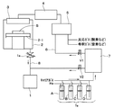
以下、本発明の実施の形態に係わる薄膜製造装置の一構成例を示す図1を参照して説明する。 A description will be given below with reference to FIG. 1 showing an example of the configuration of a thin film manufacturing apparatus according to an embodiment of the present invention.
図1に示すCVD薄膜製造装置は、真空排気システム1と、この排気システムに圧力調整バルブ1aを介して接続された反応室2と、この反応室の上部に設けられたシャワープレート3と、ガス活性化手段4と、ガス混合器5と、この混合器5に原料ガス配管6により接続された気化システムである気化器7とを有している。気化器7で気化された原料は、混合器5内で反応ガス及び希釈ガスと混合され、この混合ガスがシャワープレート3に導入される。従来の装置では、この混合ガスを直接シャワープレートへ導入していたが、本発明では、シャワープレート3と混合器5との間にガス活性化手段4を設け、混合ガスをこのガス活性化手段を通してシャワープレートに導入する。このガス活性化手段は、例えばガス配管であってもよい。気化器7と混合器5との間の配管6にはバルブV1が、また、気化器7と排気システム1との間の配管8にはバルブV2が設けられ、これにより気化器7、混合器5、排気システム1を遮断できるように構成されている。これは、気化器7、混合器5及び排気システム1の構成要素の各々のメンテナンスサイクルが異なるため、大気開放により成膜に悪影響を及ぼす水分等の物質がこれら構成要素に付着するのを避けることが目的である。1つの構成要素を大気開放してメンテナンスしている場合に、他の2つの構成要素をも大気開放することなく、真空を保持しうるように構成されている。 The CVD thin film manufacturing apparatus shown in FIG. 1 includes an
上記ガス活性化手段4には、例えばヒーター、紫外線加熱装置、マイクロ波加熱装置、又はプラズマ加熱装置等のような加熱手段が設けられている。この加熱手段で、ガス活性化手段を原料ガスの液化、析出、成膜が起こらない温度に維持し、混合ガスがガス活性化手段を通過する間に、良好な膜特性を得ることができる段階に原料を気相分解し、得られた適切な金属原子含有分子を含む混合ガスを反応室内へ供給できるようにする。そのため、使用する原料にも依るが、ガス活性化手段の温度を室温〜400℃、好ましくは165〜360℃、より好ましくは165〜250℃に設定して成膜プロセスを行う。この設定温度が低すぎると、原料ガスの析出等が起こって、パーティクルの発生につながり、また、高すぎると原料の分解が進みすぎ、その結果としてパーティクルの発生につながるという問題がある。なお、ガス活性化手段を通った混合ガスは直接シャワープレートへ導入することが好ましい。 The gas activation means 4 is provided with a heating means such as a heater, an ultraviolet heating device, a microwave heating device, or a plasma heating device. With this heating means, the gas activating means is maintained at a temperature that does not cause liquefaction, precipitation, and film formation of the source gas, and good film characteristics can be obtained while the mixed gas passes through the gas activating means. The raw material is vapor-phase decomposed, and the resulting mixed gas containing appropriate metal atom-containing molecules can be supplied into the reaction chamber. Therefore, although depending on the raw material to be used, the film forming process is performed by setting the temperature of the gas activation means to room temperature to 400 ° C, preferably 165 to 360 ° C, more preferably 165 to 250 ° C. If the set temperature is too low, the deposition of raw material gas occurs and leads to the generation of particles, and if it is too high, the decomposition of the raw material proceeds excessively, resulting in the generation of particles. The mixed gas that has passed through the gas activation means is preferably introduced directly into the shower plate.
以下、上記各構成要素について詳細に説明する。 Hereafter, each said component is demonstrated in detail.
反応室2には、成膜対象物である基板Sを載置するための、基板加熱手段を有する基板ステージ2−1が配設されており、この加熱された基板上にシャワープレート3から成膜用の混合ガスが導入される。基板Sとの反応に使用されなかった余剰の混合ガスや、基板等との反応により生じた混合ガスとの副生成物ガスや、反応物ガスが排気システム1により排気される。シャワープレート3は適度に加熱され、導入ガスが液化、析出、成膜しない温度に保たれている。 The
この反応室2の上部に設けられたシャワープレート3には、混合ガス中に存在するパーティクルを捕獲するためのフィルターとしてのパーティクル捕獲器が配設されていてもよい。このパーティクル捕獲器は、シャワープレートのシャワーホール直前に設けられていても良く、反応に必要な特定の気化した原料元素を付着・捕獲しない温度に適切に調整されていることが望ましい。 The
上記排気システム1と反応室2との間に設けられた圧力調整バルブ1aにより、様々な成膜圧力条件に容易に対応することが出来る。 Various film forming pressure conditions can be easily accommodated by the pressure regulating valve 1a provided between the
混合器5は、バルブV1が設けられている配管6により気化器7に接続されると共に、バルブ、熱交換器、マスフローコントローラ(図示せず)を介してそれぞれ二つのガス源(例えば、酸素などの酸化ガス源:窒素などの不活性ガスである希釈ガス源)にも連結されている。混合器5内で均一に混合されて得られた混合ガスは、ガス活性化手段4を経てシャワープレート3を介して反応室2へ導入され、室内において層流になることなく基板ステージ2−1上に載置された成膜対象物表面に供給される。 The
混合器5では、酸化ガス源から供給される適度に加熱された酸化ガスと、気化器7により生じ、液化、析出、成膜しない温度に保たれた配管6を経て送られる原料ガスと、不活性ガスとが導入・混合され、混合ガスが得られる。この原料ガスは、1種類の又は複数の種類のガスが混じったガスである。かくして得られた混合ガスは、ガス活性化手段4を経て反応室2内に導入される。 In the
このガス活性化手段4及び配管6はVCR継手で接続されていてもよく、各継手のVCRガスケットは、ただのリングではなく穴のところがパーティクル捕獲器となっているVCR型パーティクル捕獲器であっても良い。このVCR型パーティクル捕獲器のある継手部は、原料ガスが液化、析出、成膜しない温度に設定・保持され、かつ、反応に必要な特定の気化した原料元素を付着・捕獲しないようにすることが望ましい。 The gas activation means 4 and the
ガス混合器5とシャワープレート3との間に設けたガス活性化手段4には、混合ガスの切替えを行うバルブが混合器5の2次側に設けてあってもよい。このバルブの下流側は、反応室2に接続されている。成膜時にはこのバルブを開け、成膜終了後にこのバルブを閉じる。 In the gas activating means 4 provided between the
気化器7には、原料供給部7aと気化部(図示せず)とが接続されている。この気化器は、加圧ガス(例えば、Heガス等の不活性ガス)により液体・固体原料を有機溶媒に溶解した原料液A、B、Cを加圧・搬送し、圧送された原料液のそれぞれの流量を各液体流量制御器で制御して、キャリアガスにより気化部に運ぶように構成されている。気化部は、流量の制御された原料液を効率よく気化させ、気化して得られた原料ガスを混合器5へ供給することができるように構成されている。この気化部では、液体原料が1種の場合は単液を、液体原料が複数の場合は複数の原料液を混合して気化させることができる。原料液を気化させる際は、原料液の液滴を気化させるだけでなく、液滴にガスを当てたり、物理的な振動を与えたり又は超音波を当てたりして、気化部の壁面に設けたノズルを介して更に細かい液粒として気化部内に導入して気化させ、気化効率を上げることが好ましい。気化部の内部には、液滴又は液粒が、効率良く気化すべき箇所で極力気化することができるように、かつ、各種パーティクル捕獲器による液粒気化負荷の軽減のために、Al等の熱伝導の良い材料で作製された気化部材が配置されることが好ましい。また、気化部の内部には、原料液が気化する際に発生する残渣を元とするパーティクルを気化部外に出さないようにするために、また、少量流れ来る液滴が気化器外に真空により吸い込まれることなく気化できるようにするために、パーティクル捕獲器を設けてもよい。この気化部材とパーティクル捕獲器においては、これらに接触した液滴、細かい液粒が確実に気化できるように、かつ、反応に必要な特定の気化した原料元素を付着・捕獲しないように、適切な温度に気化条件が保たれていることが望ましい。なお、この気化器7は、原料溶解用の溶媒Dを有し、その流量を流量制御器で制御して気化部へ導入して気化部で気化させ、この溶媒ガスを作ることが可能なように構成されていてもよい。この溶媒ガスを用いて装置内部をクリーニングできる。 A raw material supply unit 7 a and a vaporization unit (not shown) are connected to the vaporizer 7. This vaporizer pressurizes and conveys the raw material liquids A, B, and C obtained by dissolving a liquid / solid raw material in an organic solvent with a pressurized gas (for example, an inert gas such as He gas). Each flow rate is controlled by each liquid flow rate controller, and is transported to the vaporization section by the carrier gas. The vaporizing section is configured to efficiently vaporize the raw material liquid whose flow rate is controlled and supply the raw material gas obtained by the vaporization to the
上記したように、本発明の薄膜製造装置は、好ましくは円筒形状の反応室2を有しており、この反応室の内部には、シリコンウェハー等の基板が載置される円筒形状の基板ステージ2−1が設けられている。この基板ステージには、基板を加熱するための加熱手段が組み込まれている。また、反応室2は、基板ステージ2−1を反応室の成膜位置と反応室下方の基板搬送位置との間で昇降自在に構成するための手段を備えていてもよい。反応室2上側の中央部には、基板ステージ2−1に対向してシャワープレート3が設けられ、パーティクルの除去された混合ガスがシャワープレート3から基板の中央部に向かって噴出されるように構成されている。 As described above, the thin film manufacturing apparatus of the present invention preferably has a
ところで、MOCVD法等のCVD法により基板上に薄膜を製造する場合、原料ガスがある温度以下に低下すると、原料ガスがパーティクルとして析出し、反応室内での成膜ダストの原因ともなる。そのため、酸化ガス用配管にガス温度調節手段である熱交換器を設けたり、また、原料ガスの析出を防止するために反応室2の外壁や基板ステージ2−1にヒータ等の加熱手段を設けてある。 Incidentally, when a thin film is produced on a substrate by a CVD method such as the MOCVD method, when the source gas is lowered below a certain temperature, the source gas is precipitated as particles, which may cause film formation dust in the reaction chamber. Therefore, a heat exchanger as a gas temperature adjusting means is provided in the oxidizing gas pipe, and a heating means such as a heater is provided on the outer wall of the
図1の薄膜製造装置を用い、本発明の製造方法を実施すれば、原料源としての有機金属化合物、例えば、液体原料としてPb(DPM)2、Zr(DMHD)4、Ti(i−PrO)2(DPM)2を用いて行う強誘電体膜PZTのCVD成膜や、液体原料としてBa(DPM)2、Sr(DPM)2、Ti(i−PrO)2(DPM)2を用いて行う強誘電体膜BSTのCVD成膜が可能であると共に、Cu、Al等のメタル配線用途を主とした薄膜や、TiN、TaN、ZrN、VN、NbN、Al2O3等のバリア用途を主とした薄膜や、その他にSBT、STO等の誘電体薄膜をCVD法により製造することができる。If the manufacturing method of this invention is implemented using the thin film manufacturing apparatus of FIG. 1, for example, Pb (DPM) 2 , Zr (DMHD) 4 , Ti (i-PrO) as a liquid source, as a raw material source. 2 (DPM) 2 is used to form a ferroelectric film PZT, and Ba (DPM) 2 , Sr (DPM) 2 , and Ti (i-PrO) 2 (DPM) 2 are used as liquid raw materials. Ferroelectric film BST can be formed by CVD, thin film mainly used for metal wiring such as Cu and Al, and barrier use such as TiN, TaN, ZrN, VN, NbN, and Al 2 O 3 In addition, a dielectric thin film such as SBT or STO can be manufactured by the CVD method.
本発明では、常温で気体、液体又は固体である原料を用い、この原料を加熱気化した原料ガスを用いることができる。この原料ガスとして、液体原料又は固体原料が溶媒に溶解されているものを気化したガスを用いることもできる。 In the present invention, it is possible to use a raw material gas obtained by heating and vaporizing this raw material using a raw material which is gas, liquid or solid at normal temperature. As the source gas, a gas obtained by vaporizing a liquid source or a solid source dissolved in a solvent may be used.
本発明の別の実施の形態によれば、図1に示す混合器5とシャワープレート3との間に設けられたガス活性化手段4として機能する上記加熱手段を備えた配管を用い、この配管を通して、混合ガスを反応室内へ導入することもできる。この配管は、例えばその内壁表面積が4.8×10⁻³m2〜1.28×10⁻¹m2の範囲であれば、所望のガス活性化を図れる。配管をこのように構成することにより、原料ガスが活性化され、良好なエビタキシャル成長が実現できる。すなわち、反応室内へ導入する原料の分解段階が適切になり、所望の金属含有分子を得ることができるので、成膜を効率良く行い、かつ、膜特性(例えば、リーク電流密度、分極反転電荷密度、分極飽和電圧等)を向上させることができる。配管の内壁表面積が4.8×10⁻³m2未満であると、有機材料ガスの分解が不十分で膜中酸素欠損が多くなり、また、内壁表面積が大きすぎると、原料ガスの気相分解が起こり、配管内壁等への膜付着による成膜速度の減少及び原料消費量の増加や、装置表面積の増大及び温調部分の増加によるコストアップなどの問題があるので、内壁表面積は1.28×10⁻¹m2程度が許容され得る好ましい上限である。なお、配管の内径にもよるが、通常用いられる内径(10.5〜25mm程度)の場合、配管長さは150〜1625mm程度あれば、同様な効果が得られる。According to another embodiment of the present invention, a pipe provided with the heating means functioning as the gas activating means 4 provided between the
本発明によれば、製造する酸化物薄膜中の所定の原子が拡散しやすい基板を用いる場合、初期層中のその原子の量を拡散しにくい基板の場合より多くすることが好ましい。これにより、所望のエピタキシャル成長を実現することができる。例えば、PtやSRO等のPbが拡散しやすい基板を用いる場合、シード層(初期層)のPb組成割合を多くすることにより、異相が無く、低電圧で自発分極が飽和する強誘電体膜を製造できる。この点に関しては、後述する図15〜22から明らかである。 According to the present invention, when a substrate in which a predetermined atom in the oxide thin film to be manufactured is easy to diffuse is used, it is preferable to increase the amount of the atom in the initial layer as compared with the case in which the substrate is difficult to diffuse. Thereby, desired epitaxial growth can be realized. For example, when using a substrate that easily diffuses Pb, such as Pt or SRO, by increasing the Pb composition ratio of the seed layer (initial layer), a ferroelectric film that has no heterogeneous phase and has a spontaneous polarization saturated at a low voltage is obtained. Can be manufactured. This point is apparent from FIGS. 15 to 22 described later.
上記したような構成を有する本発明によれば、酸素欠陥を改善することができる。更に、核成長時のシード層(初期層)を成膜する際の酸化ガス流量割合を低くし、その後膜成長時の酸化ガス流量割合を初期層の場合より高くして連続成膜することにより、エピタキシャル成長が促進され、配向が整い、リーク電流密度が低く、低電圧で自発分極が飽和する強誘電体薄膜の製造を実現できる。 According to the present invention having the configuration as described above, oxygen defects can be improved. Furthermore, by continuously forming the film by reducing the oxidizing gas flow rate when forming the seed layer (initial layer) during the nucleus growth and then increasing the oxidizing gas flow rate during film growth as compared with the initial layer. It is possible to produce a ferroelectric thin film in which epitaxial growth is promoted, orientation is aligned, leakage current density is low, and spontaneous polarization is saturated at a low voltage.
以下、図1に示す薄膜製造装置を用いて本発明の薄膜製造方法に従い、MOCVD法によりPZT強誘電体薄膜を製造する例について説明する。 Hereinafter, an example of manufacturing a PZT ferroelectric thin film by MOCVD according to the thin film manufacturing method of the present invention using the thin film manufacturing apparatus shown in FIG. 1 will be described.
固体原料のPb(thd)2、Zr(dmhd)4、Ti(i−PrO)2(thd)2をそれぞれテトラヒドロフラン(THF)溶媒に0.3mol/Lの濃度で溶かした原料の入った容器A、B及びC並びにTHFの入った容器Dをヘリウムにより加圧し、キャリアガスである窒素により気化器7へ輸送し、そこで気化した。気化して得られた原料ガスを配管6を通してガス混合器5へ輸送し、そこで酸化ガスである酸素(流量3500sccm)及び希釈ガス(キャリアガス)である窒素(300sccm)と混合し、次いでこの混合ガスをガス活性化手段4を経てシャワープレート3へ輸送し、このシャワープレートを通して、反応室2内に載置された620℃に加熱された基板S上に導入し、PZT薄膜を堆積させ、成膜せしめた。Container A containing raw materials prepared by dissolving Pb (thd) 2 , Zr (dmhd) 4 , and Ti (i-PrO) 2 (thd) 2 as solid raw materials in tetrahydrofuran (THF) solvent at a concentration of 0.3 mol / L. , B and C, and a container D containing THF were pressurized with helium and transported to the vaporizer 7 with nitrogen as a carrier gas, where it was vaporized. The raw material gas obtained by vaporization is transported to the
上記プロセスにおいて、反応室圧力は、圧力調整バルブ1aにより667Pa程度に調圧した。一般的に、反応室は133.3Pa〜3999Pa程度に調圧されるので、ガス活性化手段4の圧力は、反応室よりやや高い圧力になる。また、ガス活性化手段の温度は、原料の析出が起こらないように調整する必要があり、本実施例で用いるPb(thd)2錯体等の場合は、210℃〜250℃程度に調整した。In the above process, the reaction chamber pressure was regulated to about 667 Pa by the pressure regulating valve 1a. Generally, since the reaction chamber is regulated to about 133.3 Pa to 3999 Pa, the pressure of the gas activation means 4 is slightly higher than that of the reaction chamber. Further, the temperature of the gas activation means needs to be adjusted so that the raw material does not precipitate. In the case of the Pb (thd) 2 complex used in this example, it was adjusted to about 210 ° C. to 250 ° C.
なお、本実施例では、上記したように、基板Sの温度を基板ステージ2−1の加熱により620℃に維持して成膜を行ったが、一般には、成膜プロセスは500〜650℃程度の温度で行われる。 In this embodiment, as described above, film formation was performed while maintaining the temperature of the substrate S at 620 ° C. by heating the substrate stage 2-1, but generally the film formation process is about 500 to 650 ° C. At a temperature of
上記基板としては、Si上に形成された熱酸化SiO2膜表面に下部電極が成膜された基板を用いた。この下部電極としては、Pt、Ir、Rh、Ru、MgO、SrTiO3、IrO2、RuO2、SrRuO3、LaNiO3などのような、ある面方位に配向したものを用いることができるが、本実施例では、Ir/SiO2/Si、Pt/Ti/SiO2/Si及びSRO/Pt/Ti/SiO2/Siを用いた。As the substrate, a substrate in which a lower electrode was formed on the surface of a thermally oxidized SiO 2 film formed on Si was used. As this lower electrode, an electrode oriented in a certain plane direction such as Pt, Ir, Rh, Ru, MgO, SrTiO 3 , IrO 2 , RuO 2 , SrRuO 3 , LaNiO 3, etc. can be used. In the examples, Ir / SiO 2 / Si, Pt / Ti / SiO 2 / Si and SRO / Pt / Ti / SiO 2 / Si were used.
図2に示すように、下部電極上に、上記した手順に従ってPZT強誘電体酸化物薄膜を100nmの厚さで成膜し、更に、得られたPZT強誘電体酸化物薄膜の電気特性を評価するために、この薄膜上に上部電極としてPt膜を直径0.3mmマスクスルースパッタにより形成せしめた。この構造物を以下の実施例でサンプルとして用いて、各種評価を行った。 As shown in FIG. 2, a PZT ferroelectric oxide thin film having a thickness of 100 nm is formed on the lower electrode in accordance with the procedure described above, and the electrical properties of the obtained PZT ferroelectric oxide thin film are evaluated. In order to achieve this, a Pt film as an upper electrode was formed on this thin film by mask through sputtering with a diameter of 0.3 mm. Various evaluations were performed using this structure as a sample in the following examples.
本実施例では、PZT薄膜特性に対するガス混合器−シャワープレート間に設けたガス活性化手段の内壁表面積依存性について述べる。。 In this embodiment, the dependence of the gas activation means provided between the gas mixer and the shower plate on the PZT thin film characteristics will be described. .
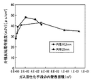
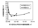
図3に、PZT薄膜の1.5V印加時のリーク電流密度(A/m2)に対するガス活性化手段の内壁表面積(m2)依存性を示す。この場合、反応室2に流れる酸素ガスの全供給ガスに対する割合は91%とした。基板にはIr(111)配向膜を用いた。リーク電流密度は、ガス活性化手段を用いない時(内壁表面積0m2)、2.5E−6A/cm2であり、内壁表面積が4.8E−3m2の時、2.0E−7であったが、内壁表面積を大きくすると減少し、内壁表面積が2.1E−2m2の時、最小値7.5E−8A/cm2を示した。内壁表面積をさらに大きくすると、リーク電流密度は上昇し、内壁表面積が5.2E−2m2の時、1.7E−7A/cm2であった。FIG. 3 shows the dependency of the gas activation means on the inner wall surface area (m 2 ) with respect to the leakage current density (A / m 2 ) of the PZT thin film when 1.5 V is applied. In this case, the ratio of the oxygen gas flowing into the
図4に、PZT薄膜の2.0V印加時の分極反転電荷密度に対するガス活性化手段の内表面積依存性を示す。この場合、酸素ガスの流量及び基板は上記と同じとした。分極反転電荷密度は、ガス活性化手段を用いない時、28μC/cm2であり、内壁表面積が4.8E−3m2の時、39μC/cm2であったが、内壁表面積を大きくすると上昇し、内壁表面積が2.1E−2m2の時、最大値48μC/cm2を示した。内壁表面積をさらに大きくすると、分極反転電荷密度は下降し、内壁表面積が5.2E−2m2の時、40μC/cm2であった。FIG. 4 shows the dependence of the gas activating means on the internal surface area of the PZT thin film with respect to the polarization inversion charge density when 2.0 V is applied. In this case, the flow rate of oxygen gas and the substrate were the same as described above. Polarization inversion charge density, when not using the gas activation means is 28μC / cm 2, when the inner wall surface area of 4.8E-3m 2, was the 39μC / cm 2, increased by increasing the inner wall surface When the inner wall surface area was 2.1E-2m 2 , the maximum value was 48 μC / cm 2 . When the inner wall surface area was further increased, the domain-inverted charge density decreased and was 40 μC / cm 2 when the inner wall surface area was 5.2E-2m 2 .
図5に、PZT薄膜の分極飽和電圧に対するガス活性化手段の内壁表面積依存性を示す。この場合、酸素ガスの流量及び基板は上記と同じとした。分極飽和電圧は、ガス活性化手段を用いない時、2.2Vであり、4.8E−3m2の時、1.90Vであったが、内壁表面積を大きくすると減少し、内壁表面積が2.1E−2m2の時、最小値1.7Vを示した。内壁表面積をさらに大きくすると、分極飽和密度は上昇し、内壁表面積が5.2E−2m2の時、1.83Vであった。FIG. 5 shows the dependence of the gas activation means on the inner wall surface area with respect to the polarization saturation voltage of the PZT thin film. In this case, the flow rate of oxygen gas and the substrate were the same as described above. The polarization saturation voltage was 2.2 V when the gas activation means was not used, and 1.90 V when 4.8E-3m 2 , but decreased when the inner wall surface area was increased, and the inner wall surface area was 2.2. when 1E-2m 2, showing the minimum value 1.7V. When the inner wall surface area was further increased, the polarization saturation density increased and was 1.83 V when the inner wall surface area was 5.2E-2m 2 .
上記したように、現在でも明確には解明されていないが、本発明で用いるような有機原料はそもそもその分解過程で少なくとも数十種類の中間体や安定な分子(THF溶媒の場合には、200種類以上の中間体や安定分子)に分解していくと推察されている。その中の極く一部の金属原子を含む分子が成膜に寄与していると考えられている。本実施例の結果は、どの分解段階の金属原子を含む分子を反応室に導入し、基板上で反応させるかにより膜特性(リーク電流密度、分極反転電荷密度、分極飽和電圧)が異なる事を示している。 As described above, although not clearly clarified at present, organic raw materials as used in the present invention are originally at least several tens of kinds of intermediates and stable molecules (in the case of THF solvent, 200 in the decomposition process). It is speculated that it will be decomposed into more than kinds of intermediates and stable molecules. Among them, molecules containing a very small part of metal atoms are considered to contribute to film formation. The result of this example is that the film properties (leakage current density, polarization inversion charge density, polarization saturation voltage) differ depending on which decomposition stage metal atom containing molecule is introduced into the reaction chamber and reacted on the substrate. Show.
本発明者らは、金属原子を含む分子の分解段階を見極めて、成膜を効率良く行いかつ膜特性を向上させるためには、気化して得た原料ガスに酸化ガスを混合した後、気相分解状態をコントロールするガス活性化手段を設け、良好な膜特性を得ることができる段階にした金属原子含有分子をシャワープレートを通して反応室へ導入しなければならないことを見出した。 In order to perform the film formation efficiently and improve the film characteristics by identifying the decomposition stage of the molecule containing the metal atom, the present inventors mixed the oxidizing gas with the raw material gas obtained by vaporization, It has been found that a gas activation means for controlling the phase decomposition state is provided, and metal atom-containing molecules in a stage capable of obtaining good film characteristics must be introduced into the reaction chamber through a shower plate.
本実施例では、PZT薄膜特性に対する酸素流量割合依存性について述べる。 In this example, the oxygen flow rate dependency on the PZT thin film characteristics will be described.
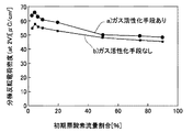
図6に、PZT薄膜の1.5V印加時のリーク電流密度に対する混合ガス中の全導入ガス基準の酸素流量割合依存性を示す。この場合、酸素流量割合は0.5〜95%と変化させ、ガス活性化手段の内壁表面積は、2.1E−2m2に設定し、基板にはIr(111)配向膜を用いた。酸素流量割合が1%の時、リーク電流密度は1E−1であり、酸素流量割合の上昇に伴い、徐々にリーク電流密度は低下していった。FIG. 6 shows the oxygen flow rate ratio dependence of the total introduced gas reference in the mixed gas with respect to the leakage current density when 1.5 V is applied to the PZT thin film. In this case, the oxygen flow rate ratio was changed to 0.5 to 95%, the inner wall surface area of the gas activation means was set to 2.1E-2m 2 , and an Ir (111) oriented film was used as the substrate. When the oxygen flow rate ratio was 1%, the leak current density was 1E-1, and as the oxygen flow rate ratio increased, the leak current density gradually decreased.
しかし、図7に示すように、PZT薄膜のXRD測定結果では、酸素流量割合5%(図中のa)と比較して、酸素流量割合80%(図中のb)では、(111)配向強度が著しく低下していた。図7の場合、Pb/(Zr+Ti)=1.15である。図8に、XRD測定によるPZT薄膜のすべての配向強度中のPZT(111)強度割合に対する酸素流量割合依存性を示す。酸素流量割合は0.5〜95%と変化させて行った。XRD(111)強度の割合は、酸素流量割合の増加に伴い減少した。このように、リーク電流密度の低減とエピタキシャル成長とはトレードオフの関係にあることが分かる。 However, as shown in FIG. 7, in the XRD measurement results of the PZT thin film, the (111) orientation was obtained at an oxygen flow rate of 80% (b in the figure) as compared to an oxygen flow rate of 5% (a in the figure). The strength was significantly reduced. In the case of FIG. 7, Pb / (Zr + Ti) = 1.15. FIG. 8 shows the oxygen flow rate ratio dependence on the PZT (111) intensity ratio in all orientation strengths of the PZT thin film by XRD measurement. The oxygen flow rate ratio was changed from 0.5 to 95%. The proportion of XRD (111) intensity decreased with increasing oxygen flow rate. Thus, it can be seen that the reduction in leakage current density and the epitaxial growth are in a trade-off relationship.
そこで、本実施例では、核発生時の初期層成膜で用いる混合ガス中の酸素流量割合(以下、初期層酸素流量割合と称す)を変化させて(0.5〜60%)エピタキシャル成長を行い、その上に連続して酸素流量割合91%の第二層目の膜を作製せしめた。かくして得られたPZT薄膜に対する膜特性を検討し、その結果を図9〜14に示す。 Therefore, in this example, the epitaxial growth is performed by changing the oxygen flow rate ratio (hereinafter referred to as the initial layer oxygen flow rate ratio) in the mixed gas used in the initial layer film formation at the time of nucleus generation (0.5 to 60%). Then, a second layer film having an oxygen flow rate ratio of 91% was continuously formed thereon. The film characteristics for the PZT thin film thus obtained were examined, and the results are shown in FIGS.
図9に、PZT薄膜の1.5V印加時のリーク電流密度に対する初期層酸素流量割合依存性を示す。この場合、初期層の厚さは5nmとし、第二層目の厚さは100nmとした。リーク電流密度は、初期層酸素流量割合5%で最小値2E−9を示し、初期層酸素流量割合の増加と共に増加した。図9から、初期層の酸素流量割合が0.5%でも十分リーク電流密度は低く、60%未満程度までは所望の値が得られ、好ましくは20%程度までであることが分かる。 FIG. 9 shows the dependency of the initial layer oxygen flow rate on the leakage current density when a 1.5 V voltage is applied to the PZT thin film. In this case, the thickness of the initial layer was 5 nm, and the thickness of the second layer was 100 nm. The leakage current density showed a minimum value 2E-9 at an initial layer oxygen flow rate ratio of 5%, and increased with an increase in the initial layer oxygen flow rate ratio. FIG. 9 shows that the leakage current density is sufficiently low even when the oxygen flow rate ratio of the initial layer is 0.5%, and a desired value is obtained up to about 60%, preferably up to about 20%.
図10に、PZT薄膜の2.0V印加時の分極反転電荷密度に対する初期層酸素流量割合依存性を示す。分極反転電荷密度は、初期層酸素流量割合5%で最大値66μC/cm2を示し、その後、初期層酸素流量割合の増加と共に減少した。図10から、初期層酸素流量割合0.5%程度でも十分分極反転電荷密度が高く、60%未満程度までは所望の値が得られ、好ましくは20%程度までであることが分かる。FIG. 10 shows the dependency of the initial layer oxygen flow rate on the polarization inversion charge density when 2.0 V is applied to the PZT thin film. The polarization inversion charge density showed a maximum value of 66 μC / cm 2 at an initial layer oxygen flow rate of 5%, and then decreased with an increase in the initial layer oxygen flow rate. FIG. 10 shows that the polarization inversion charge density is sufficiently high even at an initial layer oxygen flow rate ratio of about 0.5%, and a desired value is obtained up to about 60%, preferably up to about 20%.
図11に、分極飽和電圧に対する初期層酸素流量割合依存性を示す。分極飽和電圧は、初期層酸素流量割合5%で最小値1.29Vを示し、その後、初期層酸素流量割合の増加と共に減少した。図11から、初期層酸素流量割合0.5%程度でも十分低く、60%未満程度までは所望の値が得られ、好ましくは20%程度までであることが分かる。 FIG. 11 shows the dependence of the initial layer oxygen flow rate on the polarization saturation voltage. The polarization saturation voltage showed a minimum value of 1.29 V at an initial layer oxygen flow rate of 5%, and then decreased with an increase in the initial layer oxygen flow rate. FIG. 11 shows that the initial layer oxygen flow rate ratio of about 0.5% is sufficiently low, and a desired value is obtained up to about 60%, preferably up to about 20%.
図12、13、14に、PZT薄膜の1.5V印加時のリーク電流密度、PZT薄膜の2.0V印加時の分極反転電荷密度及び分極飽和電圧に対する初期層酸素流量割合依存性について、ガス活性化手段がある場合(図中のa、内壁表面積2.1E−2m2)とない場合とのデータを示す。これらの図から、ガス活性化手段がある場合には、ガス活性化手段がない場合と比べると、全ての酸素流量割合(0.5〜95%)に対して、低リーク電流密度、高分極反転電荷密度及び低分極飽和電圧が得られ、優れた膜特性を示すことがわかる。12, 13, and 14 show the gas activity of the leakage current density when 1.5 V is applied to the PZT thin film, the polarization inversion charge density when 2.0 V is applied to the PZT thin film, and the dependency of the initial layer oxygen flow rate on the polarization saturation voltage. The data with and without the conversion means (a in the figure, inner wall surface area 2.1E-2m 2 ) and without. From these figures, when there is a gas activation means, compared with the case without the gas activation means, for all oxygen flow rate ratios (0.5-95%), low leakage current density, high polarization It can be seen that an inverted charge density and a low polarization saturation voltage are obtained, and excellent film characteristics are exhibited.
本実施例では、Pt基板上に成膜されたPZT薄膜特性について初期核を形成する初期層Pb/(Zr+Ti)組成依存性について述べる。この場合、ガス混合器−シャワープレート間のガス活性化手段の内壁表面積は、2.08E−02m2に設定し、基板としてPt/Ti/SiO2/Si基板を用いた。In this example, the dependency of the PZT thin film formed on the Pt substrate on the composition of the initial layer Pb / (Zr + Ti) forming the initial nucleus will be described. In this case, the inner wall surface area of the gas activation means between the gas mixer and the shower plate was set to 2.08E-02m 2 , and a Pt / Ti / SiO 2 / Si substrate was used as the substrate.
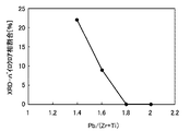
まず、単一層成膜として、酸素流量割合を91%として成膜プロセスを実施した。図15に、得られたPZT薄膜のXRD測定結果を示す。Pb/(Zr+Ti)=1.15(図15中のa)の膜は、PZTのペロブスカイト相に関するピークが観測されず、パイロクロア相のみが観測された。また、Pb/(Zr+Ti)=1.80(図15中のb)の膜は、PZTペロブスカイト単相が観測された。図16に、XRD強度パイロクロア相割合に対するPb/(Zr+Ti)組成依存性を示す。Pb/(Zr+Ti)=1.80以上では、PZTのみに配向が観測された。ただし、これらのPZT単相膜は非常にリーク電流密度が大きく、強誘電特性が得られない。 First, as a single layer film formation, a film formation process was performed with an oxygen flow rate ratio of 91%. FIG. 15 shows the XRD measurement results of the obtained PZT thin film. In the film of Pb / (Zr + Ti) = 1.15 (a in FIG. 15), no peak related to the perovskite phase of PZT was observed, and only the pyrochlore phase was observed. In addition, a PZT perovskite single phase was observed in the film of Pb / (Zr + Ti) = 1.80 (b in FIG. 15). FIG. 16 shows the Pb / (Zr + Ti) composition dependence on the XRD strength pyrochlore phase ratio. When Pb / (Zr + Ti) = 1.80 or more, orientation was observed only in PZT. However, these PZT single-phase films have a very large leakage current density, and ferroelectric properties cannot be obtained.
次いで、シード層としての初期層及び第二層の連続成膜により、特性の改善を図った。初期核を形成する初期層を、酸素流量割合5%、膜厚5nmとし、Pb(Zr+Ti)組成比を変化させて成膜した。この初期層の上に、酸素流量割合91%、膜厚100nmの膜を形成した。 Next, the characteristics were improved by continuously forming an initial layer and a second layer as a seed layer. An initial layer for forming initial nuclei was formed with an oxygen flow rate ratio of 5% and a film thickness of 5 nm, and the Pb (Zr + Ti) composition ratio was changed. On the initial layer, a film having an oxygen flow rate ratio of 91% and a film thickness of 100 nm was formed.
図17に、XRD強度パイロクロア相割合に対する初期層Pb/(Zr+Ti)組成依存性を示す。この図から、Pb/(Zr+Ti)=1.69以上でPZT単相が得られていることが推測される。 FIG. 17 shows the dependence of the initial layer Pb / (Zr + Ti) composition on the XRD strength pyrochlore phase ratio. From this figure, it is inferred that a PZT single phase is obtained at Pb / (Zr + Ti) = 1.69 or more.
図18に、分極反転電荷密度に対する初期層Pb/(Zr+Ti)組成依存性を示す。分極反転電荷密度は、Pb/(Zr+Ti)組成の増加と共に増加し、Pb/(Zr+Ti)=1.75で最大値52μC/cm2を示した。それ以上では、分極反転電荷密度は緩やかに減少した。FIG. 18 shows the dependence of the initial layer Pb / (Zr + Ti) composition on the polarization inversion charge density. The polarization inversion charge density increased with an increase in the Pb / (Zr + Ti) composition, and showed a maximum value of 52 μC / cm 2 at Pb / (Zr + Ti) = 1.75. Above that, the polarization inversion charge density decreased slowly.
図19に、分極飽和電圧に対する初期層Pb/(Zr+Ti)組成依存性を示す。分極飽和電圧は、Pb/(Zr+Ti)組成の増加と共に減少し、Pb/(Zr+Ti)=1.75で最小値1.56Vを示し、1.75を超えると緩やかに上昇した。 FIG. 19 shows the dependency of the initial layer Pb / (Zr + Ti) composition on the polarization saturation voltage. The polarization saturation voltage decreased with an increase in the Pb / (Zr + Ti) composition, showed a minimum value of 1.56 V when Pb / (Zr + Ti) = 1.75, and gradually increased when it exceeded 1.75.
これらの結果より、Pb/(Zr+Ti)=1.69から1.82までの間でPZT単相が得られており、Pb/(Zr+Ti)=1.93ではPbOの常誘電層が混在していると推測される。 From these results, a PZT single phase was obtained between Pb / (Zr + Ti) = 1.69 and 1.82, and when Pb / (Zr + Ti) = 1.93, a PbO paraelectric layer was mixed. It is estimated that
本実施例では、SrRuO3(SRO)基板上に成膜されたPZT薄膜特性に対する初期層Pb/(Zr+Ti)組成依存性について述べる。In this example, the dependency of the initial layer Pb / (Zr + Ti) composition on the properties of the PZT thin film formed on the SrRuO 3 (SRO) substrate will be described.
SRO基板においても、PbがSRO中に拡散することが確認されており、本実施例でも、初期層及び第二層の連続成膜を行い、PZT膜特性の初期層Pb/(Zr+Ti)組成依存性を調べた。 Also in the SRO substrate, it was confirmed that Pb diffuses into the SRO. In this example, the initial layer and the second layer are continuously formed, and the PZT film characteristic depends on the composition of the initial layer Pb / (Zr + Ti). I examined the sex.
図20に、XRD強度パイロクロア相割合に対する初期層Pb/(Zr+Ti)組成依存性を示す。この場合、ガス活性化手段の内壁表面積を2.08E−2m2に設定し、基板としてSRO/Pt/Ti/SiO2/Si基板を用いた。初期層成膜の際の酸素流量割合を91%、二層目成膜の際の酸素流量割合を91%にして成膜した。この図から明らかなように、Pb/(Zr+Ti)組成の増加とともにパイロクロア相割合は減少し、Pb/(Zr+Ti)=1.31以上でゼロになった。FIG. 20 shows the dependence of the initial layer Pb / (Zr + Ti) composition on the XRD strength pyrochlore phase ratio. In this case, the inner wall surface area of the gas activation means was set to 2.08E-2m 2 , and an SRO / Pt / Ti / SiO 2 / Si substrate was used as the substrate. The film was formed with an oxygen flow rate ratio of 91% during the initial layer deposition and an oxygen flow rate ratio of 91% during the second layer deposition. As is clear from this figure, the pyrochlore phase ratio decreased with an increase in the Pb / (Zr + Ti) composition, and became zero when Pb / (Zr + Ti) = 1.31 or more.
図21に、分極反転電荷密度に対する初期層Pb/(Zr+Ti)組成依存性を示す。分極反転電荷密度は、Pb/(Zr+Ti)組成の増加とともに増加し、Pb/(Zr+Ti)=1.31で最大値56μC/cm2を示した。FIG. 21 shows the dependency of the polarization inversion charge density on the composition of the initial layer Pb / (Zr + Ti). The polarization inversion charge density increased with an increase in the Pb / (Zr + Ti) composition, and showed a maximum value of 56 μC / cm 2 at Pb / (Zr + Ti) = 1.31.
図22に、分極飽和電圧に対する初期層Pb/(Zr+Ti)組成依存性を示す。分極反転密度は、Pb/(Zr+Ti)組成の増加とともに減少し、Pb/(Zr+Ti)=1.31で最小値1.41Vを示した。 FIG. 22 shows the dependency of the initial layer Pb / (Zr + Ti) composition on the polarization saturation voltage. The polarization inversion density decreased with an increase in the Pb / (Zr + Ti) composition, and showed a minimum value of 1.41 V at Pb / (Zr + Ti) = 1.31.
図20〜22から、Pb/(Zr+Ti)=1.31以上でPZT単相が得られ、膜特性も所望の値になることが分かる。しかし、膜厚が100nm程度になると、過剰なPbが粒界に析出して、リーク電流密度が大きくなることが考えられる。そこで、図20〜22に示すようPbリッチな膜を初期層に利用して、第二層ではPbを減らして連続成膜するようにすることにより本発明の目的が達成されうる。 20 to 22, it can be seen that a PZT single phase is obtained when Pb / (Zr + Ti) = 1.31 or more, and the film characteristics also have desired values. However, when the film thickness is about 100 nm, it is considered that excess Pb precipitates at the grain boundaries and the leakage current density increases. Therefore, the object of the present invention can be achieved by using a Pb-rich film as an initial layer as shown in FIGS. 20 to 22 and continuously forming a film by reducing Pb in the second layer.
次いで、ガス活性化手段として内径の異なる配管を用い、上記実施例に従ってPZT薄膜を製造して、その特性を比較した。以下の表1に、配管内径が10.2mm及び25mmである場合の配管内壁表面積と配管長さとの関係を示す。 Subsequently, PZT thin films were manufactured according to the above-described examples using pipes having different inner diameters as gas activation means, and their characteristics were compared. Table 1 below shows the relationship between the pipe inner wall surface area and the pipe length when the pipe inner diameter is 10.2 mm and 25 mm.

ガス活性化手段として上記配管を備えた薄膜製造装置を用いてPZT薄膜を製造した場合の反応室2に流れる酸素ガスの全供給ガス(混合ガス)に対する割合は、図3の場合と同様に91%とした。図23に、得られたPZT薄膜に対して、1.5V印加時のリーク電流密度(A/cm2)に対する活性化手段である配管の内壁表面積依存性を示す。この図から明らかなように、リーク電流密度は、内壁表面積が同じであれば、内径が異なってもほぼ同じ効果が得られることが分かる。The ratio of the oxygen gas flowing into the
上記と同様にして得られたPZT薄膜について、図24に2.0V印加時の分極反転電荷密度、図25に分極飽和電圧に対するガス活性化手段である配管の内壁表面積依存性をそれぞれ示す。これらの図から明らかなように、リーク電流密度の場合と同様に、内壁表面積が同じであれば、内径が異なってもほぼ同じ効果が得られることが分かる。 For the PZT thin film obtained in the same manner as described above, FIG. 24 shows the polarization inversion charge density when 2.0 V is applied, and FIG. 25 shows the dependence on the inner wall surface area of the pipe as gas activation means with respect to the polarization saturation voltage. As can be seen from these figures, as in the case of the leakage current density, if the inner wall surface area is the same, the same effect can be obtained even if the inner diameter is different.
1 真空排気システム 1a 圧力調整バルブ
2 反応室 3 シャワープレート
4 ガス活性化手段 5 ガス混合器
6 原料ガス配管 7 気化器
7a 原料供給部 8 配管
S 基板DESCRIPTION OF
本発明によれば、所定の酸素分圧になるような酸化ガス流量割合を用いて成膜することにより、又は核成長時のシード層である初期層の酸素分庄を下げ、その後膜成長時の酸化ガス流量割合を上げて連続成膜することにより、エピタキシャル成長が促進され、配向が整い、かつ、リーク電流が少なく、低電圧で自発分極が飽和する強誘電体薄膜を実現することができた。また、良好な膜特性を得る事の出来る段階に分解した金属原子を含む分子を反応室に導入して強誘電体薄膜の製造に用いる事ができるので、酸素欠陥が改善された薄膜を製造することができた。かくして、良好な膜特性を有する強誘電体薄膜を製造する方法を提供できた。また、ガス混合器とシャワープレートとの間にガス活性化手段を設けることにより、酸素欠陥が改善された薄膜の製造装置を提供できた。かくして、この製造方法及び製造装置は、半導体素子の製造分野において極めて有用である。 According to the present invention, a film is formed by using an oxidizing gas flow rate ratio that gives a predetermined oxygen partial pressure, or the oxygen concentration of the initial layer, which is a seed layer at the time of nuclear growth, is lowered, and then the film is grown. By continuously increasing the oxidizing gas flow rate of the film, it was possible to realize a ferroelectric thin film that promotes epitaxial growth, aligns orientation, has little leakage current, and saturates spontaneous polarization at a low voltage. . In addition, since molecules containing metal atoms decomposed to a stage where good film properties can be obtained can be introduced into the reaction chamber and used for the production of ferroelectric thin films, thin films with improved oxygen defects are produced. I was able to. Thus, a method for producing a ferroelectric thin film having good film properties could be provided. Further, by providing a gas activation means between the gas mixer and the shower plate, a thin film manufacturing apparatus with improved oxygen defects can be provided. Thus, this manufacturing method and manufacturing apparatus are extremely useful in the field of manufacturing semiconductor devices.
Claims (9)
前記ガス混合器と前記シャワープレートとの間に設けられ、内壁表面積が4.8×10⁻³m2〜1.28×10⁻¹m2である配管を備え、シャワープレートへ導入される際の原料ガスが所望の膜特性が得られる金属原子含有分子に気相分解される温度に加熱されたガス活性化手段を通して、前記混合ガスを前記反応室内に供給し、
前記酸化ガスの流量割合が混合ガス基準で60%以上であることを特徴とする酸化物薄膜製造方法。The raw material gas, carrier gas, and oxidizing gas that vaporize the raw material for the oxide thin film are mixed in a gas mixer, and the obtained mixed gas is supplied to the substrate heated in the reaction chamber of the chemical vapor deposition apparatus through the shower plate. In the method of producing an oxide thin film on a substrate,
When the pipe is provided between the gas mixer and the shower plate and has an inner wall surface area of 4.8 × 10 −3 m 2 to 1.28 × 10 −1 m 2 , and is introduced into the shower plate The mixed gas is supplied into the reaction chamber through a gas activation means heated to a temperature at which the raw material gas is vapor-phase decomposed into metal atom-containing molecules with desired film characteristics.
A method for producing an oxide thin film, wherein a flow rate ratio of the oxidizing gas is 60% or more based on a mixed gas.
前記混合ガスを前記ガス混合器と前記シャワープレートとの間に設けられたガス活性化手段を通して反応室内に供給するものであって、
前記混合ガスを前記反応室内に供給してシード層としての初期層を成膜する工程と、
前記初期層を成膜する工程で供給された混合ガスよりも高い酸化ガス流量割合を有する混合ガスを前記反応室内に供給して前記初期層の上に第二層を連続して成膜する工程と、を含むことを特徴とする酸化物薄膜製造方法。The raw material gas, carrier gas, and oxidizing gas that vaporize the raw material for the oxide thin film are mixed in a gas mixer, and the obtained mixed gas is supplied to the substrate heated in the reaction chamber of the chemical vapor deposition apparatus through the shower plate. In the method of producing an oxide thin film on a substrate,
Supplying the mixed gas into a reaction chamber through gas activating means provided between the gas mixer and the shower plate,
Supplying the mixed gas into the reaction chamber to form an initial layer as a seed layer;
Supplying a mixed gas having a higher flow rate of oxidizing gas than the mixed gas supplied in the step of forming the initial layer into the reaction chamber to continuously form a second layer on the initial layer. And a method for producing an oxide thin film.
Applications Claiming Priority (3)
| Application Number | Priority Date | Filing Date | Title |
|---|---|---|---|
| JP2003300014 | 2003-08-25 | ||
| JP2003300014 | 2003-08-25 | ||
| PCT/JP2004/012180 WO2005020311A1 (en) | 2003-08-25 | 2004-08-25 | Process for producing oxide thin film and production apparatus therefor |
Publications (2)
| Publication Number | Publication Date |
|---|---|
| JPWO2005020311A1 JPWO2005020311A1 (en) | 2007-11-01 |
| JP4628954B2 true JP4628954B2 (en) | 2011-02-09 |
Family
ID=34213796
Family Applications (1)
| Application Number | Title | Priority Date | Filing Date |
|---|---|---|---|
| JP2005513346A Active JP4628954B2 (en) | 2003-08-25 | 2004-08-25 | Oxide thin film manufacturing method |
Country Status (7)
| Country | Link |
|---|---|
| US (1) | US20070054472A1 (en) |
| EP (1) | EP1662556B1 (en) |
| JP (1) | JP4628954B2 (en) |
| KR (2) | KR101179098B1 (en) |
| CN (1) | CN100435294C (en) |
| TW (1) | TW200511404A (en) |
| WO (1) | WO2005020311A1 (en) |
Families Citing this family (7)
| Publication number | Priority date | Publication date | Assignee | Title |
|---|---|---|---|---|
| JP2008053683A (en) * | 2006-07-27 | 2008-03-06 | Matsushita Electric Ind Co Ltd | Insulating film forming method, semiconductor device, and substrate processing apparatus |
| EP2053642A4 (en) * | 2006-08-02 | 2011-01-05 | Ulvac Inc | Film-forming method and film-forming apparatus |
| JP2010080813A (en) * | 2008-09-29 | 2010-04-08 | Fujifilm Corp | Piezoelectric film and method of manufacturing the same, piezoelectric device, and liquid discharge apparatus |
| TWI452946B (en) * | 2009-12-29 | 2014-09-11 | Univ Nat Yunlin Sci & Tech | Plasma reaction device |
| JP2014150191A (en) * | 2013-02-01 | 2014-08-21 | Ulvac Japan Ltd | Pzt film manufacturing method and deposition apparatus |
| CN106367732B (en) * | 2016-09-22 | 2018-11-06 | 四川大学 | A kind of medium temperature metal organic chemical vapor deposition TiO2-Al2O3Composite coating device and painting method |
| CN110586180B (en) * | 2019-09-20 | 2022-06-14 | 湖南师范大学 | Visible light catalysis N has2Preparation method of ruthenium hybrid deca-poly quaternary ammonium tungstate with O participating in selective oxidation |
Citations (6)
| Publication number | Priority date | Publication date | Assignee | Title |
|---|---|---|---|---|
| JPH0883793A (en) * | 1994-06-08 | 1996-03-26 | Hyundai Electron Ind Co Ltd | Formation of ferroelectric thin film |
| JPH08268797A (en) * | 1995-03-30 | 1996-10-15 | Hitachi Ltd | Chemical vapor phase reaction deposition device |
| JPH11126877A (en) * | 1997-07-18 | 1999-05-11 | Ramtron Internatl Corp | Multilayered method for optimizing performance of ferroelectric thin film |
| JP2000058525A (en) * | 1998-08-03 | 2000-02-25 | Nec Corp | Vapor growth method for metal oxide dielectric film |
| JP2003086586A (en) * | 2001-09-13 | 2003-03-20 | Murata Mfg Co Ltd | Orientational ferroelectric thin film element and method for manufacturing the same |
| JP2003324101A (en) * | 2002-04-30 | 2003-11-14 | Fujitsu Ltd | Manufacturing method of semiconductor device |
Family Cites Families (9)
| Publication number | Priority date | Publication date | Assignee | Title |
|---|---|---|---|---|
| JPH086181B2 (en) * | 1992-11-30 | 1996-01-24 | 日本電気株式会社 | Chemical vapor deposition method and chemical vapor deposition apparatus |
| US5989998A (en) * | 1996-08-29 | 1999-11-23 | Matsushita Electric Industrial Co., Ltd. | Method of forming interlayer insulating film |
| JPH1131650A (en) * | 1997-07-14 | 1999-02-02 | Kokusai Electric Co Ltd | Antireflection coating, substrate to be treated, manufacture of the substrate to be treated, manufacture of fine pattern and manufacture of semiconductor device |
| EP1143501A4 (en) * | 1998-12-16 | 2005-02-02 | Tokyo Electron Ltd | Method of forming thin film |
| US6495878B1 (en) * | 1999-08-02 | 2002-12-17 | Symetrix Corporation | Interlayer oxide containing thin films for high dielectric constant application |
| US6811651B2 (en) * | 2001-06-22 | 2004-11-02 | Tokyo Electron Limited | Gas temperature control for a plasma process |
| US20030012875A1 (en) * | 2001-07-10 | 2003-01-16 | Shreyas Kher | CVD BST film composition and property control with thickness below 200 A for DRAM capacitor application with size at 0.1mum or below |
| US6713127B2 (en) * | 2001-12-28 | 2004-03-30 | Applied Materials, Inc. | Methods for silicon oxide and oxynitride deposition using single wafer low pressure CVD |
| US6884464B2 (en) * | 2002-11-04 | 2005-04-26 | Applied Materials, Inc. | Methods for forming silicon comprising films using hexachlorodisilane in a single-wafer deposion chamber |
-
2004
- 2004-08-25 JP JP2005513346A patent/JP4628954B2/en active Active
- 2004-08-25 EP EP04772141.0A patent/EP1662556B1/en active Active
- 2004-08-25 CN CNB2004800243173A patent/CN100435294C/en active Active
- 2004-08-25 WO PCT/JP2004/012180 patent/WO2005020311A1/en active Application Filing
- 2004-08-25 US US10/569,470 patent/US20070054472A1/en not_active Abandoned
- 2004-08-25 KR KR1020067003747A patent/KR101179098B1/en active IP Right Grant
- 2004-08-25 KR KR1020117021973A patent/KR101246499B1/en active IP Right Grant
- 2004-08-26 TW TW093125554A patent/TW200511404A/en unknown
Patent Citations (6)
| Publication number | Priority date | Publication date | Assignee | Title |
|---|---|---|---|---|
| JPH0883793A (en) * | 1994-06-08 | 1996-03-26 | Hyundai Electron Ind Co Ltd | Formation of ferroelectric thin film |
| JPH08268797A (en) * | 1995-03-30 | 1996-10-15 | Hitachi Ltd | Chemical vapor phase reaction deposition device |
| JPH11126877A (en) * | 1997-07-18 | 1999-05-11 | Ramtron Internatl Corp | Multilayered method for optimizing performance of ferroelectric thin film |
| JP2000058525A (en) * | 1998-08-03 | 2000-02-25 | Nec Corp | Vapor growth method for metal oxide dielectric film |
| JP2003086586A (en) * | 2001-09-13 | 2003-03-20 | Murata Mfg Co Ltd | Orientational ferroelectric thin film element and method for manufacturing the same |
| JP2003324101A (en) * | 2002-04-30 | 2003-11-14 | Fujitsu Ltd | Manufacturing method of semiconductor device |
Also Published As
| Publication number | Publication date |
|---|---|
| TWI363377B (en) | 2012-05-01 |
| KR20110116065A (en) | 2011-10-24 |
| WO2005020311A1 (en) | 2005-03-03 |
| US20070054472A1 (en) | 2007-03-08 |
| TW200511404A (en) | 2005-03-16 |
| EP1662556A4 (en) | 2012-05-09 |
| CN1842901A (en) | 2006-10-04 |
| KR101246499B1 (en) | 2013-03-25 |
| KR20060118418A (en) | 2006-11-23 |
| EP1662556A1 (en) | 2006-05-31 |
| KR101179098B1 (en) | 2012-09-03 |
| JPWO2005020311A1 (en) | 2007-11-01 |
| CN100435294C (en) | 2008-11-19 |
| EP1662556B1 (en) | 2013-11-06 |
Similar Documents
| Publication | Publication Date | Title |
|---|---|---|
| JP5719849B2 (en) | Thin film manufacturing method | |
| JP3462852B2 (en) | Method and apparatus for producing thin films by chemical vapor deposition | |
| US6787181B2 (en) | Chemical vapor deposition method of making layered superlattice materials using trimethylbismuth | |
| Isobe et al. | Characteristics of ferroelectric SrBi2Ta2O9 thin films grown by “flash” MOCVD | |
| KR100945096B1 (en) | Method for manufacturing capacitor | |
| JP4628954B2 (en) | Oxide thin film manufacturing method | |
| JPH08176826A (en) | Thin film depositing device by cvd, deposition method and cvd material and liquid material vessel used in the device or method | |
| US20080248595A1 (en) | Method for Manufacturing Semiconductor Device and Computer Storage Medium | |
| JP2009129963A (en) | Film formation method, film-forming apparatus, and method for manufacturing semiconductor device | |
| WO2000008680A1 (en) | Vapor growth method for metal oxide dielectric film and vapor growth device for metal oxide dielectric material | |
| JPWO2012042772A1 (en) | Thin film manufacturing method and thin film manufacturing apparatus | |
| JP4205565B2 (en) | Thin film manufacturing method | |
| JP4243171B2 (en) | Method for forming metal oxide thin film | |
| JPH09241849A (en) | Apparatus for production of oxide thin film and its production | |
| US20050167713A1 (en) | Ferroelectric capacitor and method of production of same | |
| JP3886921B2 (en) | Chemical vapor deposition method | |
| JP4473540B2 (en) | Thin film manufacturing method and particle number evaluation method | |
| JP2006351827A (en) | Film-formation method | |
| JP2003224118A (en) | Device and method for depositing film |
Legal Events
| Date | Code | Title | Description |
|---|---|---|---|
| A621 | Written request for application examination |
Free format text: JAPANESE INTERMEDIATE CODE: A621 Effective date: 20070801 |
|
| A131 | Notification of reasons for refusal |
Free format text: JAPANESE INTERMEDIATE CODE: A131 Effective date: 20100518 |
|
| A521 | Request for written amendment filed |
Free format text: JAPANESE INTERMEDIATE CODE: A523 Effective date: 20100720 |
|
| A131 | Notification of reasons for refusal |
Free format text: JAPANESE INTERMEDIATE CODE: A131 Effective date: 20100810 |
|
| A521 | Request for written amendment filed |
Free format text: JAPANESE INTERMEDIATE CODE: A523 Effective date: 20101001 |
|
| TRDD | Decision of grant or rejection written | ||
| A01 | Written decision to grant a patent or to grant a registration (utility model) |
Free format text: JAPANESE INTERMEDIATE CODE: A01 Effective date: 20101026 |
|
| A01 | Written decision to grant a patent or to grant a registration (utility model) |
Free format text: JAPANESE INTERMEDIATE CODE: A01 |
|
| A61 | First payment of annual fees (during grant procedure) |
Free format text: JAPANESE INTERMEDIATE CODE: A61 Effective date: 20101110 |
|
| FPAY | Renewal fee payment (event date is renewal date of database) |
Free format text: PAYMENT UNTIL: 20131119 Year of fee payment: 3 |
|
| R150 | Certificate of patent or registration of utility model |
Ref document number: 4628954 Country of ref document: JP Free format text: JAPANESE INTERMEDIATE CODE: R150 Free format text: JAPANESE INTERMEDIATE CODE: R150 |
|
| R250 | Receipt of annual fees |
Free format text: JAPANESE INTERMEDIATE CODE: R250 |
|
| R250 | Receipt of annual fees |
Free format text: JAPANESE INTERMEDIATE CODE: R250 |
|
| R250 | Receipt of annual fees |
Free format text: JAPANESE INTERMEDIATE CODE: R250 |
|
| R250 | Receipt of annual fees |
Free format text: JAPANESE INTERMEDIATE CODE: R250 |
|
| R250 | Receipt of annual fees |
Free format text: JAPANESE INTERMEDIATE CODE: R250 |
|
| R250 | Receipt of annual fees |
Free format text: JAPANESE INTERMEDIATE CODE: R250 |
|
| R250 | Receipt of annual fees |
Free format text: JAPANESE INTERMEDIATE CODE: R250 |
|
| R250 | Receipt of annual fees |
Free format text: JAPANESE INTERMEDIATE CODE: R250 |
|
| R250 | Receipt of annual fees |
Free format text: JAPANESE INTERMEDIATE CODE: R250 |
|
| R250 | Receipt of annual fees |
Free format text: JAPANESE INTERMEDIATE CODE: R250 |