CN100435294C - Process for producing oxide thin film and production apparatus therefor - Google Patents
Process for producing oxide thin film and production apparatus therefor Download PDFInfo
- Publication number
- CN100435294C CN100435294C CNB2004800243173A CN200480024317A CN100435294C CN 100435294 C CN100435294 C CN 100435294C CN B2004800243173 A CNB2004800243173 A CN B2004800243173A CN 200480024317 A CN200480024317 A CN 200480024317A CN 100435294 C CN100435294 C CN 100435294C
- Authority
- CN
- China
- Prior art keywords
- gas
- sull
- film
- thin film
- substrate
- Prior art date
- Legal status (The legal status is an assumption and is not a legal conclusion. Google has not performed a legal analysis and makes no representation as to the accuracy of the status listed.)
- Active
Links
- 238000000034 method Methods 0.000 title claims abstract description 55
- 238000004519 manufacturing process Methods 0.000 title claims abstract description 48
- 230000008569 process Effects 0.000 title claims abstract description 20
- 239000010409 thin film Substances 0.000 title abstract description 52
- 239000007789 gas Substances 0.000 claims abstract description 179
- 229910052760 oxygen Inorganic materials 0.000 claims abstract description 73
- QVGXLLKOCUKJST-UHFFFAOYSA-N atomic oxygen Chemical compound [O] QVGXLLKOCUKJST-UHFFFAOYSA-N 0.000 claims abstract description 71
- 239000001301 oxygen Substances 0.000 claims abstract description 71
- 239000000758 substrate Substances 0.000 claims abstract description 60
- 239000002994 raw material Substances 0.000 claims abstract description 25
- 239000012159 carrier gas Substances 0.000 claims abstract description 13
- 239000000203 mixture Substances 0.000 claims abstract description 10
- 230000004913 activation Effects 0.000 claims description 54
- 238000002309 gasification Methods 0.000 claims description 35
- 230000001590 oxidative effect Effects 0.000 claims description 33
- 239000008246 gaseous mixture Substances 0.000 claims description 32
- 239000012528 membrane Substances 0.000 claims description 21
- 239000012071 phase Substances 0.000 claims description 20
- 239000000463 material Substances 0.000 claims description 16
- 230000008676 import Effects 0.000 claims description 15
- 238000000354 decomposition reaction Methods 0.000 claims description 12
- 239000002184 metal Substances 0.000 claims description 11
- 229910052751 metal Inorganic materials 0.000 claims description 11
- 238000009434 installation Methods 0.000 claims description 10
- 239000013078 crystal Substances 0.000 claims description 9
- IJGRMHOSHXDMSA-UHFFFAOYSA-N nitrogen Substances N#N IJGRMHOSHXDMSA-UHFFFAOYSA-N 0.000 claims description 8
- 239000000126 substance Substances 0.000 claims description 8
- 239000012808 vapor phase Substances 0.000 claims description 8
- 229910002367 SrTiO Inorganic materials 0.000 claims description 6
- 229910010413 TiO 2 Inorganic materials 0.000 claims description 6
- 239000011261 inert gas Substances 0.000 claims description 6
- 229910052757 nitrogen Inorganic materials 0.000 claims description 5
- XKRFYHLGVUSROY-UHFFFAOYSA-N Argon Chemical compound [Ar] XKRFYHLGVUSROY-UHFFFAOYSA-N 0.000 claims description 4
- 229910004298 SiO 2 Inorganic materials 0.000 claims description 4
- 229910004121 SrRuO Inorganic materials 0.000 claims description 4
- 229910052697 platinum Inorganic materials 0.000 claims description 4
- 229910052726 zirconium Inorganic materials 0.000 claims description 4
- 241000877463 Lanio Species 0.000 claims description 3
- 239000001307 helium Substances 0.000 claims description 3
- 229910052734 helium Inorganic materials 0.000 claims description 3
- SWQJXJOGLNCZEY-UHFFFAOYSA-N helium atom Chemical compound [He] SWQJXJOGLNCZEY-UHFFFAOYSA-N 0.000 claims description 3
- 229910052741 iridium Inorganic materials 0.000 claims description 3
- CPLXHLVBOLITMK-UHFFFAOYSA-N magnesium oxide Inorganic materials [Mg]=O CPLXHLVBOLITMK-UHFFFAOYSA-N 0.000 claims description 3
- 229910052703 rhodium Inorganic materials 0.000 claims description 3
- 229910052707 ruthenium Inorganic materials 0.000 claims description 3
- CBENFWSGALASAD-UHFFFAOYSA-N Ozone Chemical compound [O-][O+]=O CBENFWSGALASAD-UHFFFAOYSA-N 0.000 claims description 2
- 229910052786 argon Inorganic materials 0.000 claims description 2
- 229910052743 krypton Inorganic materials 0.000 claims description 2
- DNNSSWSSYDEUBZ-UHFFFAOYSA-N krypton atom Chemical compound [Kr] DNNSSWSSYDEUBZ-UHFFFAOYSA-N 0.000 claims description 2
- 229910052754 neon Inorganic materials 0.000 claims description 2
- GKAOGPIIYCISHV-UHFFFAOYSA-N neon atom Chemical compound [Ne] GKAOGPIIYCISHV-UHFFFAOYSA-N 0.000 claims description 2
- QJGQUHMNIGDVPM-UHFFFAOYSA-N nitrogen group Chemical group [N] QJGQUHMNIGDVPM-UHFFFAOYSA-N 0.000 claims description 2
- 239000010408 film Substances 0.000 abstract description 93
- 230000003213 activating effect Effects 0.000 abstract description 8
- 230000007547 defect Effects 0.000 abstract description 8
- 238000007254 oxidation reaction Methods 0.000 abstract description 8
- 230000003647 oxidation Effects 0.000 abstract description 7
- 238000006243 chemical reaction Methods 0.000 abstract description 6
- 238000010438 heat treatment Methods 0.000 abstract description 6
- 230000001737 promoting effect Effects 0.000 abstract description 3
- 238000002156 mixing Methods 0.000 abstract description 2
- 230000008021 deposition Effects 0.000 abstract 1
- 230000006911 nucleation Effects 0.000 abstract 1
- 238000010899 nucleation Methods 0.000 abstract 1
- 230000010287 polarization Effects 0.000 description 45
- 239000007788 liquid Substances 0.000 description 20
- 239000002245 particle Substances 0.000 description 15
- 230000015572 biosynthetic process Effects 0.000 description 8
- 238000005755 formation reaction Methods 0.000 description 8
- 239000002904 solvent Substances 0.000 description 8
- 238000000605 extraction Methods 0.000 description 6
- WYURNTSHIVDZCO-UHFFFAOYSA-N Tetrahydrofuran Chemical compound C1CCOC1 WYURNTSHIVDZCO-UHFFFAOYSA-N 0.000 description 5
- 229920006395 saturated elastomer Polymers 0.000 description 5
- 230000001925 catabolic effect Effects 0.000 description 4
- 230000000694 effects Effects 0.000 description 4
- 239000011368 organic material Substances 0.000 description 4
- 230000002269 spontaneous effect Effects 0.000 description 4
- 230000002950 deficient Effects 0.000 description 3
- 238000005516 engineering process Methods 0.000 description 3
- 230000009467 reduction Effects 0.000 description 3
- 239000011343 solid material Substances 0.000 description 3
- 230000008859 change Effects 0.000 description 2
- 238000013461 design Methods 0.000 description 2
- 238000010586 diagram Methods 0.000 description 2
- 238000009792 diffusion process Methods 0.000 description 2
- 238000012423 maintenance Methods 0.000 description 2
- 238000005086 pumping Methods 0.000 description 2
- 238000011160 research Methods 0.000 description 2
- 230000000630 rising effect Effects 0.000 description 2
- 239000004065 semiconductor Substances 0.000 description 2
- 229910052710 silicon Inorganic materials 0.000 description 2
- 239000007787 solid Substances 0.000 description 2
- MEYZYGMYMLNUHJ-UHFFFAOYSA-N tunicamycin Natural products CC(C)CCCCCCCCCC=CC(=O)NC1C(O)C(O)C(CC(O)C2OC(C(O)C2O)N3C=CC(=O)NC3=O)OC1OC4OC(CO)C(O)C(O)C4NC(=O)C MEYZYGMYMLNUHJ-UHFFFAOYSA-N 0.000 description 2
- XDTMQSROBMDMFD-UHFFFAOYSA-N Cyclohexane Chemical compound C1CCCCC1 XDTMQSROBMDMFD-UHFFFAOYSA-N 0.000 description 1
- XUIMIQQOPSSXEZ-UHFFFAOYSA-N Silicon Chemical compound [Si] XUIMIQQOPSSXEZ-UHFFFAOYSA-N 0.000 description 1
- ATJFFYVFTNAWJD-UHFFFAOYSA-N Tin Chemical compound [Sn] ATJFFYVFTNAWJD-UHFFFAOYSA-N 0.000 description 1
- 230000004888 barrier function Effects 0.000 description 1
- 239000006227 byproduct Substances 0.000 description 1
- 238000005229 chemical vapour deposition Methods 0.000 description 1
- 229910052802 copper Inorganic materials 0.000 description 1
- 238000002425 crystallisation Methods 0.000 description 1
- 239000003085 diluting agent Substances 0.000 description 1
- 239000000428 dust Substances 0.000 description 1
- 238000011156 evaluation Methods 0.000 description 1
- 230000004907 flux Effects 0.000 description 1
- 230000006872 improvement Effects 0.000 description 1
- 239000004615 ingredient Substances 0.000 description 1
- 239000003595 mist Substances 0.000 description 1
- 238000005457 optimization Methods 0.000 description 1
- 239000005416 organic matter Substances 0.000 description 1
- 239000003960 organic solvent Substances 0.000 description 1
- 150000002902 organometallic compounds Chemical class 0.000 description 1
- 238000012856 packing Methods 0.000 description 1
- 230000000704 physical effect Effects 0.000 description 1
- 239000000376 reactant Substances 0.000 description 1
- 239000012495 reaction gas Substances 0.000 description 1
- 230000001105 regulatory effect Effects 0.000 description 1
- 230000008439 repair process Effects 0.000 description 1
- 238000009958 sewing Methods 0.000 description 1
- 239000010703 silicon Substances 0.000 description 1
- 239000007921 spray Substances 0.000 description 1
- 239000006200 vaporizer Substances 0.000 description 1
Images


Classifications
-
- C—CHEMISTRY; METALLURGY
- C23—COATING METALLIC MATERIAL; COATING MATERIAL WITH METALLIC MATERIAL; CHEMICAL SURFACE TREATMENT; DIFFUSION TREATMENT OF METALLIC MATERIAL; COATING BY VACUUM EVAPORATION, BY SPUTTERING, BY ION IMPLANTATION OR BY CHEMICAL VAPOUR DEPOSITION, IN GENERAL; INHIBITING CORROSION OF METALLIC MATERIAL OR INCRUSTATION IN GENERAL
- C23C—COATING METALLIC MATERIAL; COATING MATERIAL WITH METALLIC MATERIAL; SURFACE TREATMENT OF METALLIC MATERIAL BY DIFFUSION INTO THE SURFACE, BY CHEMICAL CONVERSION OR SUBSTITUTION; COATING BY VACUUM EVAPORATION, BY SPUTTERING, BY ION IMPLANTATION OR BY CHEMICAL VAPOUR DEPOSITION, IN GENERAL
- C23C16/00—Chemical coating by decomposition of gaseous compounds, without leaving reaction products of surface material in the coating, i.e. chemical vapour deposition [CVD] processes
- C23C16/22—Chemical coating by decomposition of gaseous compounds, without leaving reaction products of surface material in the coating, i.e. chemical vapour deposition [CVD] processes characterised by the deposition of inorganic material, other than metallic material
- C23C16/30—Deposition of compounds, mixtures or solid solutions, e.g. borides, carbides, nitrides
- C23C16/40—Oxides
- C23C16/409—Oxides of the type ABO3 with A representing alkali, alkaline earth metal or lead and B representing a refractory metal, nickel, scandium or a lanthanide
-
- H—ELECTRICITY
- H01—ELECTRIC ELEMENTS
- H01L—SEMICONDUCTOR DEVICES NOT COVERED BY CLASS H10
- H01L21/00—Processes or apparatus adapted for the manufacture or treatment of semiconductor or solid state devices or of parts thereof
- H01L21/02—Manufacture or treatment of semiconductor devices or of parts thereof
- H01L21/02104—Forming layers
- H01L21/02365—Forming inorganic semiconducting materials on a substrate
- H01L21/02612—Formation types
- H01L21/02617—Deposition types
- H01L21/0262—Reduction or decomposition of gaseous compounds, e.g. CVD
-
- H—ELECTRICITY
- H01—ELECTRIC ELEMENTS
- H01L—SEMICONDUCTOR DEVICES NOT COVERED BY CLASS H10
- H01L21/00—Processes or apparatus adapted for the manufacture or treatment of semiconductor or solid state devices or of parts thereof
- H01L21/02—Manufacture or treatment of semiconductor devices or of parts thereof
- H01L21/02104—Forming layers
- H01L21/02107—Forming insulating materials on a substrate
- H01L21/02225—Forming insulating materials on a substrate characterised by the process for the formation of the insulating layer
- H01L21/0226—Forming insulating materials on a substrate characterised by the process for the formation of the insulating layer formation by a deposition process
- H01L21/02263—Forming insulating materials on a substrate characterised by the process for the formation of the insulating layer formation by a deposition process deposition from the gas or vapour phase
- H01L21/02271—Forming insulating materials on a substrate characterised by the process for the formation of the insulating layer formation by a deposition process deposition from the gas or vapour phase deposition by decomposition or reaction of gaseous or vapour phase compounds, i.e. chemical vapour deposition
-
- C—CHEMISTRY; METALLURGY
- C23—COATING METALLIC MATERIAL; COATING MATERIAL WITH METALLIC MATERIAL; CHEMICAL SURFACE TREATMENT; DIFFUSION TREATMENT OF METALLIC MATERIAL; COATING BY VACUUM EVAPORATION, BY SPUTTERING, BY ION IMPLANTATION OR BY CHEMICAL VAPOUR DEPOSITION, IN GENERAL; INHIBITING CORROSION OF METALLIC MATERIAL OR INCRUSTATION IN GENERAL
- C23C—COATING METALLIC MATERIAL; COATING MATERIAL WITH METALLIC MATERIAL; SURFACE TREATMENT OF METALLIC MATERIAL BY DIFFUSION INTO THE SURFACE, BY CHEMICAL CONVERSION OR SUBSTITUTION; COATING BY VACUUM EVAPORATION, BY SPUTTERING, BY ION IMPLANTATION OR BY CHEMICAL VAPOUR DEPOSITION, IN GENERAL
- C23C16/00—Chemical coating by decomposition of gaseous compounds, without leaving reaction products of surface material in the coating, i.e. chemical vapour deposition [CVD] processes
- C23C16/44—Chemical coating by decomposition of gaseous compounds, without leaving reaction products of surface material in the coating, i.e. chemical vapour deposition [CVD] processes characterised by the method of coating
- C23C16/448—Chemical coating by decomposition of gaseous compounds, without leaving reaction products of surface material in the coating, i.e. chemical vapour deposition [CVD] processes characterised by the method of coating characterised by the method used for generating reactive gas streams, e.g. by evaporation or sublimation of precursor materials
- C23C16/4481—Chemical coating by decomposition of gaseous compounds, without leaving reaction products of surface material in the coating, i.e. chemical vapour deposition [CVD] processes characterised by the method of coating characterised by the method used for generating reactive gas streams, e.g. by evaporation or sublimation of precursor materials by evaporation using carrier gas in contact with the source material
- C23C16/4482—Chemical coating by decomposition of gaseous compounds, without leaving reaction products of surface material in the coating, i.e. chemical vapour deposition [CVD] processes characterised by the method of coating characterised by the method used for generating reactive gas streams, e.g. by evaporation or sublimation of precursor materials by evaporation using carrier gas in contact with the source material by bubbling of carrier gas through liquid source material
-
- C—CHEMISTRY; METALLURGY
- C23—COATING METALLIC MATERIAL; COATING MATERIAL WITH METALLIC MATERIAL; CHEMICAL SURFACE TREATMENT; DIFFUSION TREATMENT OF METALLIC MATERIAL; COATING BY VACUUM EVAPORATION, BY SPUTTERING, BY ION IMPLANTATION OR BY CHEMICAL VAPOUR DEPOSITION, IN GENERAL; INHIBITING CORROSION OF METALLIC MATERIAL OR INCRUSTATION IN GENERAL
- C23C—COATING METALLIC MATERIAL; COATING MATERIAL WITH METALLIC MATERIAL; SURFACE TREATMENT OF METALLIC MATERIAL BY DIFFUSION INTO THE SURFACE, BY CHEMICAL CONVERSION OR SUBSTITUTION; COATING BY VACUUM EVAPORATION, BY SPUTTERING, BY ION IMPLANTATION OR BY CHEMICAL VAPOUR DEPOSITION, IN GENERAL
- C23C16/00—Chemical coating by decomposition of gaseous compounds, without leaving reaction products of surface material in the coating, i.e. chemical vapour deposition [CVD] processes
- C23C16/44—Chemical coating by decomposition of gaseous compounds, without leaving reaction products of surface material in the coating, i.e. chemical vapour deposition [CVD] processes characterised by the method of coating
- C23C16/448—Chemical coating by decomposition of gaseous compounds, without leaving reaction products of surface material in the coating, i.e. chemical vapour deposition [CVD] processes characterised by the method of coating characterised by the method used for generating reactive gas streams, e.g. by evaporation or sublimation of precursor materials
- C23C16/452—Chemical coating by decomposition of gaseous compounds, without leaving reaction products of surface material in the coating, i.e. chemical vapour deposition [CVD] processes characterised by the method of coating characterised by the method used for generating reactive gas streams, e.g. by evaporation or sublimation of precursor materials by activating reactive gas streams before their introduction into the reaction chamber, e.g. by ionisation or addition of reactive species
-
- H—ELECTRICITY
- H01—ELECTRIC ELEMENTS
- H01L—SEMICONDUCTOR DEVICES NOT COVERED BY CLASS H10
- H01L21/00—Processes or apparatus adapted for the manufacture or treatment of semiconductor or solid state devices or of parts thereof
- H01L21/02—Manufacture or treatment of semiconductor devices or of parts thereof
- H01L21/02104—Forming layers
- H01L21/02107—Forming insulating materials on a substrate
- H01L21/02109—Forming insulating materials on a substrate characterised by the type of layer, e.g. type of material, porous/non-porous, pre-cursors, mixtures or laminates
- H01L21/02112—Forming insulating materials on a substrate characterised by the type of layer, e.g. type of material, porous/non-porous, pre-cursors, mixtures or laminates characterised by the material of the layer
- H01L21/02123—Forming insulating materials on a substrate characterised by the type of layer, e.g. type of material, porous/non-porous, pre-cursors, mixtures or laminates characterised by the material of the layer the material containing silicon
- H01L21/02164—Forming insulating materials on a substrate characterised by the type of layer, e.g. type of material, porous/non-porous, pre-cursors, mixtures or laminates characterised by the material of the layer the material containing silicon the material being a silicon oxide, e.g. SiO2
-
- H—ELECTRICITY
- H01—ELECTRIC ELEMENTS
- H01L—SEMICONDUCTOR DEVICES NOT COVERED BY CLASS H10
- H01L21/00—Processes or apparatus adapted for the manufacture or treatment of semiconductor or solid state devices or of parts thereof
- H01L21/02—Manufacture or treatment of semiconductor devices or of parts thereof
- H01L21/02104—Forming layers
- H01L21/02107—Forming insulating materials on a substrate
- H01L21/02109—Forming insulating materials on a substrate characterised by the type of layer, e.g. type of material, porous/non-porous, pre-cursors, mixtures or laminates
- H01L21/02112—Forming insulating materials on a substrate characterised by the type of layer, e.g. type of material, porous/non-porous, pre-cursors, mixtures or laminates characterised by the material of the layer
- H01L21/02172—Forming insulating materials on a substrate characterised by the type of layer, e.g. type of material, porous/non-porous, pre-cursors, mixtures or laminates characterised by the material of the layer the material containing at least one metal element, e.g. metal oxides, metal nitrides, metal oxynitrides or metal carbides
- H01L21/02175—Forming insulating materials on a substrate characterised by the type of layer, e.g. type of material, porous/non-porous, pre-cursors, mixtures or laminates characterised by the material of the layer the material containing at least one metal element, e.g. metal oxides, metal nitrides, metal oxynitrides or metal carbides characterised by the metal
- H01L21/02178—Forming insulating materials on a substrate characterised by the type of layer, e.g. type of material, porous/non-porous, pre-cursors, mixtures or laminates characterised by the material of the layer the material containing at least one metal element, e.g. metal oxides, metal nitrides, metal oxynitrides or metal carbides characterised by the metal the material containing aluminium, e.g. Al2O3
-
- H—ELECTRICITY
- H01—ELECTRIC ELEMENTS
- H01L—SEMICONDUCTOR DEVICES NOT COVERED BY CLASS H10
- H01L21/00—Processes or apparatus adapted for the manufacture or treatment of semiconductor or solid state devices or of parts thereof
- H01L21/02—Manufacture or treatment of semiconductor devices or of parts thereof
- H01L21/02104—Forming layers
- H01L21/02107—Forming insulating materials on a substrate
- H01L21/02109—Forming insulating materials on a substrate characterised by the type of layer, e.g. type of material, porous/non-porous, pre-cursors, mixtures or laminates
- H01L21/02112—Forming insulating materials on a substrate characterised by the type of layer, e.g. type of material, porous/non-porous, pre-cursors, mixtures or laminates characterised by the material of the layer
- H01L21/02172—Forming insulating materials on a substrate characterised by the type of layer, e.g. type of material, porous/non-porous, pre-cursors, mixtures or laminates characterised by the material of the layer the material containing at least one metal element, e.g. metal oxides, metal nitrides, metal oxynitrides or metal carbides
- H01L21/02175—Forming insulating materials on a substrate characterised by the type of layer, e.g. type of material, porous/non-porous, pre-cursors, mixtures or laminates characterised by the material of the layer the material containing at least one metal element, e.g. metal oxides, metal nitrides, metal oxynitrides or metal carbides characterised by the metal
- H01L21/02181—Forming insulating materials on a substrate characterised by the type of layer, e.g. type of material, porous/non-porous, pre-cursors, mixtures or laminates characterised by the material of the layer the material containing at least one metal element, e.g. metal oxides, metal nitrides, metal oxynitrides or metal carbides characterised by the metal the material containing hafnium, e.g. HfO2
-
- H—ELECTRICITY
- H01—ELECTRIC ELEMENTS
- H01L—SEMICONDUCTOR DEVICES NOT COVERED BY CLASS H10
- H01L21/00—Processes or apparatus adapted for the manufacture or treatment of semiconductor or solid state devices or of parts thereof
- H01L21/02—Manufacture or treatment of semiconductor devices or of parts thereof
- H01L21/02104—Forming layers
- H01L21/02107—Forming insulating materials on a substrate
- H01L21/02109—Forming insulating materials on a substrate characterised by the type of layer, e.g. type of material, porous/non-porous, pre-cursors, mixtures or laminates
- H01L21/02112—Forming insulating materials on a substrate characterised by the type of layer, e.g. type of material, porous/non-porous, pre-cursors, mixtures or laminates characterised by the material of the layer
- H01L21/02172—Forming insulating materials on a substrate characterised by the type of layer, e.g. type of material, porous/non-porous, pre-cursors, mixtures or laminates characterised by the material of the layer the material containing at least one metal element, e.g. metal oxides, metal nitrides, metal oxynitrides or metal carbides
- H01L21/02175—Forming insulating materials on a substrate characterised by the type of layer, e.g. type of material, porous/non-porous, pre-cursors, mixtures or laminates characterised by the material of the layer the material containing at least one metal element, e.g. metal oxides, metal nitrides, metal oxynitrides or metal carbides characterised by the metal
- H01L21/02183—Forming insulating materials on a substrate characterised by the type of layer, e.g. type of material, porous/non-porous, pre-cursors, mixtures or laminates characterised by the material of the layer the material containing at least one metal element, e.g. metal oxides, metal nitrides, metal oxynitrides or metal carbides characterised by the metal the material containing tantalum, e.g. Ta2O5
-
- H—ELECTRICITY
- H01—ELECTRIC ELEMENTS
- H01L—SEMICONDUCTOR DEVICES NOT COVERED BY CLASS H10
- H01L21/00—Processes or apparatus adapted for the manufacture or treatment of semiconductor or solid state devices or of parts thereof
- H01L21/02—Manufacture or treatment of semiconductor devices or of parts thereof
- H01L21/02104—Forming layers
- H01L21/02107—Forming insulating materials on a substrate
- H01L21/02109—Forming insulating materials on a substrate characterised by the type of layer, e.g. type of material, porous/non-porous, pre-cursors, mixtures or laminates
- H01L21/02112—Forming insulating materials on a substrate characterised by the type of layer, e.g. type of material, porous/non-porous, pre-cursors, mixtures or laminates characterised by the material of the layer
- H01L21/02172—Forming insulating materials on a substrate characterised by the type of layer, e.g. type of material, porous/non-porous, pre-cursors, mixtures or laminates characterised by the material of the layer the material containing at least one metal element, e.g. metal oxides, metal nitrides, metal oxynitrides or metal carbides
- H01L21/02175—Forming insulating materials on a substrate characterised by the type of layer, e.g. type of material, porous/non-porous, pre-cursors, mixtures or laminates characterised by the material of the layer the material containing at least one metal element, e.g. metal oxides, metal nitrides, metal oxynitrides or metal carbides characterised by the metal
- H01L21/02186—Forming insulating materials on a substrate characterised by the type of layer, e.g. type of material, porous/non-porous, pre-cursors, mixtures or laminates characterised by the material of the layer the material containing at least one metal element, e.g. metal oxides, metal nitrides, metal oxynitrides or metal carbides characterised by the metal the material containing titanium, e.g. TiO2
-
- H—ELECTRICITY
- H01—ELECTRIC ELEMENTS
- H01L—SEMICONDUCTOR DEVICES NOT COVERED BY CLASS H10
- H01L21/00—Processes or apparatus adapted for the manufacture or treatment of semiconductor or solid state devices or of parts thereof
- H01L21/02—Manufacture or treatment of semiconductor devices or of parts thereof
- H01L21/02104—Forming layers
- H01L21/02107—Forming insulating materials on a substrate
- H01L21/02109—Forming insulating materials on a substrate characterised by the type of layer, e.g. type of material, porous/non-porous, pre-cursors, mixtures or laminates
- H01L21/02112—Forming insulating materials on a substrate characterised by the type of layer, e.g. type of material, porous/non-porous, pre-cursors, mixtures or laminates characterised by the material of the layer
- H01L21/02172—Forming insulating materials on a substrate characterised by the type of layer, e.g. type of material, porous/non-porous, pre-cursors, mixtures or laminates characterised by the material of the layer the material containing at least one metal element, e.g. metal oxides, metal nitrides, metal oxynitrides or metal carbides
- H01L21/02175—Forming insulating materials on a substrate characterised by the type of layer, e.g. type of material, porous/non-porous, pre-cursors, mixtures or laminates characterised by the material of the layer the material containing at least one metal element, e.g. metal oxides, metal nitrides, metal oxynitrides or metal carbides characterised by the metal
- H01L21/02189—Forming insulating materials on a substrate characterised by the type of layer, e.g. type of material, porous/non-porous, pre-cursors, mixtures or laminates characterised by the material of the layer the material containing at least one metal element, e.g. metal oxides, metal nitrides, metal oxynitrides or metal carbides characterised by the metal the material containing zirconium, e.g. ZrO2
-
- H—ELECTRICITY
- H01—ELECTRIC ELEMENTS
- H01L—SEMICONDUCTOR DEVICES NOT COVERED BY CLASS H10
- H01L21/00—Processes or apparatus adapted for the manufacture or treatment of semiconductor or solid state devices or of parts thereof
- H01L21/02—Manufacture or treatment of semiconductor devices or of parts thereof
- H01L21/02104—Forming layers
- H01L21/02107—Forming insulating materials on a substrate
- H01L21/02109—Forming insulating materials on a substrate characterised by the type of layer, e.g. type of material, porous/non-porous, pre-cursors, mixtures or laminates
- H01L21/02112—Forming insulating materials on a substrate characterised by the type of layer, e.g. type of material, porous/non-porous, pre-cursors, mixtures or laminates characterised by the material of the layer
- H01L21/02172—Forming insulating materials on a substrate characterised by the type of layer, e.g. type of material, porous/non-porous, pre-cursors, mixtures or laminates characterised by the material of the layer the material containing at least one metal element, e.g. metal oxides, metal nitrides, metal oxynitrides or metal carbides
- H01L21/02197—Forming insulating materials on a substrate characterised by the type of layer, e.g. type of material, porous/non-porous, pre-cursors, mixtures or laminates characterised by the material of the layer the material containing at least one metal element, e.g. metal oxides, metal nitrides, metal oxynitrides or metal carbides the material having a perovskite structure, e.g. BaTiO3
-
- H—ELECTRICITY
- H01—ELECTRIC ELEMENTS
- H01L—SEMICONDUCTOR DEVICES NOT COVERED BY CLASS H10
- H01L21/00—Processes or apparatus adapted for the manufacture or treatment of semiconductor or solid state devices or of parts thereof
- H01L21/02—Manufacture or treatment of semiconductor devices or of parts thereof
- H01L21/04—Manufacture or treatment of semiconductor devices or of parts thereof the devices having at least one potential-jump barrier or surface barrier, e.g. PN junction, depletion layer or carrier concentration layer
- H01L21/18—Manufacture or treatment of semiconductor devices or of parts thereof the devices having at least one potential-jump barrier or surface barrier, e.g. PN junction, depletion layer or carrier concentration layer the devices having semiconductor bodies comprising elements of Group IV of the Periodic System or AIIIBV compounds with or without impurities, e.g. doping materials
- H01L21/30—Treatment of semiconductor bodies using processes or apparatus not provided for in groups H01L21/20 - H01L21/26
- H01L21/31—Treatment of semiconductor bodies using processes or apparatus not provided for in groups H01L21/20 - H01L21/26 to form insulating layers thereon, e.g. for masking or by using photolithographic techniques; After treatment of these layers; Selection of materials for these layers
- H01L21/314—Inorganic layers
- H01L21/316—Inorganic layers composed of oxides or glassy oxides or oxide based glass
- H01L21/3165—Inorganic layers composed of oxides or glassy oxides or oxide based glass formed by oxidation
Abstract
The invention relates to a method and apparatus for manufacturing an oxide thin film. An oxide thin film having good characteristic properties is prepared by reducing an occurrence of an oxygen defect of the resulting oxide thin film and promoting the epitaxial growth of the film. The oxide thin film is prepared by admixing a raw gas, a carrier gas and an oxidation gas and supplying the resulting gas mixture on a heated substrate placed in a reaction chamber from a shower plate through a gas activating means which is maintained, by a heating means, at such a temperature that any liquefaction, deposition and film-formation of a raw material are never caused, to thus make the oxidation gas react with one another and to prepare the oxide thin film on the substrate. In this case, a rate of the oxidation gas flow rate is not less than 60% on the basis of the gas mixture. Furthermore, a flow rate of oxidation gas used for forming an initial layer by nucleation is less than 60%, and a flow rate of oxidation gas used in a subsequent film-forming process for forming a second layer is not less than 60%. Furthermore, in an apparatus for preparing the oxide thin film, a heating means is arranged between a gas-mixing unit and a shower plate.
Description
Technical field
The present invention relates to sull manufacture method and manufacturing installation thereof, particularly relate to the manufacture method and the manufacturing installation thereof of the sull that adopts chemical vapor-phase growing (CVD) method.
Background technology
In recent years, since the highly integrated demand of semiconductor device in the exploitation of the volume production technology of carrying out the good chemical vapor-phase growing method of fault tunicle energetically.Wherein, make by SiO
2, TiO
2, Al
2O
3, Ta
2O
5, MgO, ZrO
2, HfO
2, (Ba, Sr) TiO
2, SrTiO
3Deng normal dielectric oxide, Pb (Zr, Ti) O
3, SrBi
2Ta
2O
9, Bi
4Ti
3O
12Deng strong dielectric oxide constitute film the time, if thereby the oxygen in the film is damaged when influencing good epitaxial growth, normal dielectric oxide film and strong dielectric oxide film insulating properties reduce respectively.
The reduction of these characteristics results from the decomposable process of the organic material that is used for raw material.Though also do not get across clearly at present, estimate that organic material resolves into tens of kinds intermediate and stable molecule after all at least in its decomposable process.Can think that wherein the molecule of the containing metal atom of quite a few has the film forming of helping.In addition, according to the molecule of the metallic atom that contains which of decomposable process is imported film forming room in stage, whether on substrate, react the membrane property difference.If use the molecular film-forming that contains the metallic molecule that decomposes insufficient stage, then a lot of organic principles enter in the film, influence the crystallinity of film.If use the molecular film-forming of the metallic atom that contains the excessive decomposition stage, then cause gas-phase decomposition, produce a large amount of particles.Yet manufacture method does not in the past adopt the process conditions of considering this decomposable process, and device in the past can not become the device of considering this decomposable process and constitute, the result, with single crystals mutually specific characteristic do not guide fully.
CVD oxide in the past, for example Pb (Zr, Ti) O
3(below, claim PZT) strong dielectric oxide, generally also difficult anti-crystallization defective, leakage current density is about 1E-6.This occasion, if the oxygen amount (oxygen flow ratio) of increase mixing then can make leakage current density reduce, but owing to influence the motion of atom in the crystalline growth, so amorphous or with the normal dielectric layer growth of strong dielectricity different orientation, dielectric property variation by force.Otherwise, if reduce the oxygen flow ratio, then can obtain to be orientated neat film near epitaxial growth, but because residual organic matter or oxygen defect are many, so the leakage current increase in density.This PZT raw material, for example Pb (thd)
2, Zr (dmhd)
4, Ti (i-PrO)
2(thd)
2, owing to be solid at normal temperatures, carry so be dissolved in the solvent of oxolane or cyclohexane etc., at high temperature after the gasification, be blended in formation PZT film on the CVD reative cell substrate with oxygen.At this moment, simultaneously decompose one side with oxygen raw materials mixed gas and import reative cell.
Summary of the invention
Problem of the present invention is the research that solves the problem of above-mentioned conventional art, its purpose is to provide by making the oxidizing gas flow proportional, the activation optimization of unstripped gas, the oxygen of seeking to reduce the sull that organic material constitutes is damaged, promote epitaxial growth, improve membranously, can make the film-forming method and the manufacturing installation thereof of chemical vapor-phase growing method of the sull of excellent specific property.
Sull manufacture method of the present invention, it is characterized in that the unstripped gas of sull with material gasification, help the carrier gas and the oxidizing gas of transferring raw material in gas mixer, to mix, supplying with the gaseous mixture that obtains by jet tray (shower plate) on being arranged at as the heated substrates in the reative cell of chemical vapor-phase growing apparatus reacts it, on substrate, make in the method for sull, the flow proportional of oxidizing gas is pressed the gaseous mixture benchmark for more than or equal to 60%, and preferably 60%~95%.The flow proportional of oxidizing gas is lower than at 60% o'clock, because so damaged oxygen is the leakage current increase.If use oxidizing gas more than or equal to 60% flow proportional, then can realize desired epitaxial growth, obtain the few crystal of defective.In addition, because to the logical inert gas of gasifier, so the upper limit of oxidizing gas flow proportional is generally about 95%.
Sull manufacture method of the present invention, its feature is still with the unstripped gas of sull with material gasification, carrier gas and oxidizing gas mix in gas mixer, by the jet tray gaseous mixture that the supply system gets on being arranged at as the heated substrates in the reative cell of chemical vapor-phase growing apparatus it is reacted, on substrate, make in the method for sull, at first use above-mentioned gaseous mixture to be made as the initial stage tunic of crystal seed layer, adopt gaseous mixture to make second tunic continuously then with oxidizing gas flow proportional higher than initial stage layer occasion.By making layer and the second layer variation in the early stage of oxidizing gas flow proportional carry out continuous film forming, it is few to make defective, and smooth sull like this.
In the above-mentioned sull manufacture method of utilizing continuous film forming, it is characterized in that the oxidizing gas flow proportional in the initial stage layer film-forming process is lower than 60%, preferably 0.5%~60%, the oxidizing gas flow proportional in the second layer film-forming process is more than or equal to 60%, preferably 60%~95%.Oxidizing gas flow proportional in the initial stage layer film-forming process is lower than at 0.5% o'clock, and because of damaged oxygen event leakage current increases, and the oxidizing gas flow proportional surpasses at 60% o'clock, hinders epitaxial growth, the orientation variation.In addition, when the oxidizing gas flow proportional in the second layer film-forming process is lower than 60%, because of damaged oxygen event leakage current increases.
Above-mentioned sull manufacture method is characterized in that supplying with gaseous mixture by the gas activation means that are arranged between blender and the jet tray in reative cell.Like this, because the gas-phase decomposition state of control unstripped gas can be used for film forming to the molecule that reative cell imports the containing metal atom of kilter, so the membrane property of the film that makes is good.
The above-mentioned gas activating means is characterized in that maintaining the temperature of molecule that unstripped gas gas-phase decomposition when jet tray imports becomes to obtain the containing metal atom of desired membrane property.By making the gas activation means can control the gas-phase decomposition state of raw material in this wise, can make film with good membrane property.This occasion, the liquefaction that this gas activation means are maintained never produce unstripped gas, the temperature of separating out are in the scope of the temperature that does not cause the unstripped gas film forming.This temperature also depends on employed raw material, but generally is room temperature~400 ℃, preferred 165~360 ℃, is more preferably 165~250 ℃.As above-mentioned oxidizing gas, the preferred use is selected from oxygen, ozone, N
2O and NO
2Gas.
Preferably use the inert gas that is selected from nitrogen, helium, argon, neon, krypton as above-mentioned carrier gas.
As aforesaid substrate, the preferred use is selected from Pt, Ir, Rh, Ru, MgO, SrTiO
3, IrO
2, RuO
2, SrRuO
3And LaNiO
3The substrate that constitutes of material.
In the above-mentioned sull manufacture method,, can use to be selected from SiO as the sull raw material
2, TiO
2, Al
2O
3, Ta
2O
5, MgO, ZrO
2, HfO
2, (Ba, Sr) TiO
2And SrTiO
3Normal dielectric oxide, be selected from Pb (Zr, Ti) O
3, SrBi
2Ta
2O
9And Bi
4Ti
3O
12Strong dielectric oxide.
Above-mentioned sull manufacture method, the occasion that it is characterized in that making the atom stipulated in the sull by manufacturing in substrate, to spread easily, the occasion that is difficult to be diffused into substrate than the amount of this atom in the initial stage layer is many, realizes epitaxial growth.
Sull manufacturing installation of the present invention, it is characterized in that the unstripped gas of sull with material gasification, carrier gas and oxidizing gas mix in gas mixer, supplying with prepared gaseous mixture by jet tray on being arranged at as the heated substrates in the reative cell of chemical vapor-phase growing apparatus reacts it, on substrate, make in the device of sull, between blender and jet tray, establish the gas activation means.
The above-mentioned gas activating means is characterized in that having heater means.These gas activation means can be the pipe arrangements between blender and the jet tray.
According to the present invention, as above-mentioned oxidizing gas by use particular flow rate ratio, and by using the gas activation means of setting, the catabolic phase of the unstripped gas that can obtain suiting, can realize not having the good epitaxial growth of oxygen defect, the result can make the sull of excellent specific property.
According to the present invention, become the such oxidizing gas flow proportional of setting partial pressure of oxygen by utilization and carry out film forming, or the partial pressure of oxygen of the initial stage layer of the crystal seed layer when reducing as nucleus growth, oxidizing gas flow proportional when improving the film growth then carries out continuous film forming, has the promotion epitaxial growth, can realize making that to have orientation neat, and leakage current is few, the effect of the sull of the saturated good membrane property of spontaneous polarization under the low pressure.In addition, be used for the manufacturing of sull owing to the molecule at the containing metal atom that can obtain the decomposition of good membrane property stage can be imported reative cell, so can make the improved film of oxygen defect.In addition, by between gas mixer and jet tray, establishing the gas activation means, have the manufacturing installation that the film that oxygen defect is improved can be provided.
Description of drawings
Fig. 1 represents the schematic drawing of a kind of configuration example of apparatus for manufacturing thin film of the present invention.
Fig. 2 represents the schematic drawing of the sample structure that the evaluated for film characteristic is used among each embodiment.
The curve chart of the dependence of the leakage current density when Fig. 3 represents that the inner wall surface area of gas activation means and pzt thin film add 1.5V.
The curve chart of the dependence of polarization reversal charge density when Fig. 4 represents that the inner wall surface area of gas activation means and pzt thin film add 2.0V.
Fig. 5 represents the curve chart of the dependence of the inner wall surface area of gas activation means and pzt thin film polarization saturation voltage.
Fig. 6 represents the curve chart of sewing the dependence of current density when oxygen flow ratio (gaseous mixture benchmark) and pzt thin film add 1.5V.
Fig. 7 is the XRD determining figure of pzt thin film.
Fig. 8 represents that the pzt thin film of oxygen flow ratio and XRD determining all is orientated the curve chart of the dependence of PZT (111) intensity in the intensity.
The curve chart of the dependence of the leakage current density when Fig. 9 represents that initial stage layer oxygen flow ratio and pzt thin film add 1.5V.
The curve chart of the dependence of the polarization reversal charge density when Figure 10 represents that initial stage layer oxygen flow ratio and pzt thin film add 2.0V.
Figure 11 represents the curve chart of the dependence of initial stage layer oxygen flow ratio and polarization saturation voltage.
The curve chart of the dependence of the leakage current density when Figure 12 represents that relevant initial stage layer oxygen flow ratio and pzt thin film add 1.5V.
The curve chart of the dependence of the polarization reversal charge density when Figure 13 represents that relevant initial stage layer oxygen flow ratio and pzt thin film add 2.0V.
Figure 14 represents the curve chart of dependence of the polarization saturation voltage of relevant initial stage layer oxygen flow ratio and pzt thin film.
Figure 15 is the XRD determining figure of pzt thin film.
Figure 16 represents that Pb/ (Zr+Ti) forms and the XRD intensity pyrochlore curve chart of the dependency relationships of ratio mutually.
Figure 17 represents that initial stage layer Pb/ (Zr+Ti) forms and the XRD intensity pyrochlore curve chart of the dependency relationships of ratio mutually.
Figure 18 represents that initial stage layer Pb/ (Zr+Ti) forms and the curve chart of the dependency relationships of polarization reversal charge density.
Figure 19 represents that one deck Pb/ (Zr+Ti) forms and the curve chart of the dependency relationships of polarization saturation voltage.
Figure 20 represents that initial stage layer Pb/ (Zr+Ti) forms and the XRD intensity pyrochlore curve chart of the dependence of ratio mutually.
Figure 21 represents that initial stage layer Pb/ (Zr+Ti) forms and the curve chart of the dependence of polarization reversal charge density.
Figure 22 represents that initial stage layer Pb/ (Zr+Ti) forms and the curve chart of the dependence of polarization saturation voltage.
The curve chart of the dependence of the leakage current density when Figure 23 represents that the inner wall surface area of gas activation means and pzt thin film add 1.5V.
The curve chart of the dependence of the polarization reversal charge density when Figure 24 represents that the inner wall surface area of gas activation means and pzt thin film add 2.0V.
Figure 25 represents the curve chart of dependence of the polarization saturation voltage of the inner wall surface area of gas activation means and pzt thin film.
Symbol description
1 vacuum pumping system
The 1a pressure-regulating valve
2 reative cells
3 jet trays
4 gas activation means
5 gas mixers
6 unstrpped gas pipe arrangements
7 gasifiers
7a raw material supplying portion
8 pipe arrangements
The S substrate
Embodiment
According to the present invention, the film that not only adopts the individual layer film-forming process to make, and adopting change oxidizing gas flow repeatedly to be carried out to the occasion that membrane process makes film continuously, it is little also can to make leakage current density, the polarization reversal saturation voltage is little, and the film of good membrane property is arranged.The latter's continuous film forming method can obtain better characteristic.In addition, if use manufacturing installation of the present invention, can make expeditiously as above-mentioned sull.
Below, Fig. 1 of a kind of configuration example of the apparatus for manufacturing thin film that the reference expression is relevant with embodiment of the present invention describes.
The CVD apparatus for manufacturing thin film that Fig. 1 represents, has vacuum pumping system 1, with the reative cell 2 that is connected with this gas extraction system by pressure-regulating valve 1a, be located at the jet tray 3 on this reative cell top, gas activation means 4, gas mixer 5 reaches the gasifier 7 as the gasification system that is connected with this blender 5 by unstripped gas pipe arrangement 6.Raw material in gasifier 7 gasifications mixes with reaction gas and carrier gas in blender 5, and this gaseous mixture is imported in the jet tray 3.Device in the past is directly this gaseous mixture to be imported jet tray, and the present invention then establishes gas activation means 4 between jet tray 3 and blender 5, by these gas activation means gaseous mixture is imported jet tray.These gas activation means for example can be the gas pipe arrangements.Can establish valve V1 on the pipe arrangement 6 between gasifier 7 and the blender 5, can also establish valve V2 on the pipe arrangement 8 between gasifier 7 and the gas extraction system 1, this formation can be blocked gasifier 7, blender 5 and gas extraction system 1.This is because gasifier 7, and each maintenance cycle difference of the inscape of blender 5 and gas extraction system 1 its objective is and avoids causing the material that film forming is produced dysgenic moisture etc. to stick on these inscapes because of leading to atmosphere.It is formed in the occasion that a kind of structure key element is keeped in repair to atmosphere opening, can not allow other 2 kinds of inscapes lead to atmosphere, and keep vacuum.
Above-mentioned gas activating means 4 for example can be established heater, ultraviolet heater, microwave heating equipment, or the heater means of plasma heater etc. and so on.Adopt this heater means the gas activation means can be maintained the liquefaction that does not cause unstripped gas, separate out, the temperature of film forming, when gaseous mixture is by the gas activation means, the stage that can obtain good membrane property with the unstripped gas phase decomposition, in reative cell, supply with the gaseous mixture of the molecule contain gained suitable metal atom.Therefore, though, the temperature of gas activation means is set in room temperature~400 ℃, preferred 165~360 ℃, more preferably is set in 165~250 ℃ and is carried out to membrane process also according to employed raw material difference.When this design temperature is too low, cause separating out of unstripped gas etc., be related to the generation of particle, and design temperature when too high raw material decompose excessively, as a result of exist to be related to the problem that particle produces and so on.Moreover, preferably directly import gaseous mixture by the gas activation means to jet tray.
Below, above-mentioned each inscape is at length described.
In reative cell 2, set mounting and use, the substrate platform 2-1 of substrate heater means is arranged, import the gaseous mixture that film forming is used to this heated substrate from jet tray 3 as the substrate S of film forming object.With substrate S reaction in the remaining gaseous mixture that do not use, or the byproduct gas of the gaseous mixture that produces with reaction, or reactant gas carries out exhaust through gas extraction system 1 with substrate etc.Jet tray 3 is moderately heated, and remains on importing gas and does not liquefy, and separates out the temperature of film forming.
Be located on the jet tray 3 on these reative cell 2 tops, can set the particle trapping device that is present in the filter that the particle in the gaseous mixture uses as catching.This particle trapping device also can be located at the spray orifice dead ahead of jet tray, preferably suitably be adjusted to do not adhere to, the temperature of the raw material element of the required specific gasification of capture reaction.
Utilization is located at the pressure-regulating valve 1a between above-mentioned gas extraction system 1 and the reative cell 2, can be easily corresponding with various film forming pressure conditions.
Import in blender 5 and mix by producing by the oxidizing gas of appropriate heating with by gasifier 7 that oxidation source gas is supplied with, the unstripped gas of not liquefying through remaining on, separate out, the pipe arrangement 6 of the temperature of film forming being carried, and inert gas obtain gaseous mixture.This unstripped gas is the gas that one or more gas mixes.The gaseous mixture that obtains like this imports in reative cell 2 through gas activation means 4.
These gas activation means 4 and pipe arrangement 6 can connect with the VCR joint, and the VCR packing ring of each joint is not common ring, but the position in hole becomes the VCR type particle trapping device of particle trapping device.The connector portions that this VCR type particle trapping device is arranged is preferably set and is remained on unstripped gas and do not liquefy, separate out, the temperature of film forming, and otherwise adhere to, the raw material element of specific gasification that capture reaction is required.
The valve that carries out the gaseous mixture switching between gas mixer 5 and jet tray 3 in the gas activation means 4 that are provided with also can be located at the primary side of blender 5.The downstream of this valve links to each other with reative cell 2.Open this valve during film forming, film forming is closed this valve after finishing.
Connecting 7a of raw material supplying portion and gasification portion (not having diagram) on the gasifier 7.Its formation of this gasifier is to utilize gas-pressurized (for example, the inert gas of He gas etc.) material liquid A, B, the C that is dissolved with liquid, solid material in the organic solvent pressurizeed and carry, use each flow of the material liquid of each liquid flow controller control institute force feed, utilize carrier gas to be transported to gasification portion.The formation of gasification portion wants to make expeditiously the controlled material liquid of flow to gasify, and the unstripped gas that gasification obtains is supplied with blender 5.This gasification portion liquid charging stock is that a kind occasion can make single liquid gasification, and liquid charging stock is to make it gasification after multiple occasion is mixed multiple material liquid.When making the material liquid gasification, be not only the droplets vaporize that makes material liquid, and preferably make gas bump against drop, or drop given the vibration of physical property or make ultrasonic wave and drop bumps against, form thinner liquid grain and import in the gasification portion and gasify by being located at nozzle on the gasification portion wall, improve gasification efficiency.Inside in gasification portion, for make drop or liquid grain should high efficiency the position of gasification can do one's utmost to gasify, and in order to alleviate the liquid grain gasification load that various particle trapping devices cause, preferred disposition is used the gasification member of the good made of conducting heat such as Al.In addition, be discharged to outside the gasification portion for the particle on basis in order not make residue that material liquid when gasification produce, and gasifier is outer can to gasify for the drop that a small amount of stream is come is not drawn onto by vacuum, also the particle trapping device can be set in the inside of gasification portion.This gasification member and particle trapping device positively gasify in order to make the drop that contacts these parts, thin liquid grain, and for the raw material element of the required specific gasification of the reaction of Adhesion catching not, preferably make gasification condition remain on suitable temperature.In addition, these gasifier 7 its formations also can be for there being the solvent D of raw material dissolving usefulness, and use traffic controller control solvent flux imports to gasification portion and makes it the gasification in gasification portion, can form this solvent gas.Can use this solvent gas cleanup device inside.
Apparatus for manufacturing thin film of the present invention as mentioned above preferably has the reative cell 2 of drum, can establish the substrate platform 2-1 of the drum of substrates such as mounting silicon chip in the inside of this reative cell.The heater means that this substrate platform combination has heated substrates to use.In addition, reative cell 2 also can be purchased between the one-tenth film location of reative cell and the substrate transferring position below the reative cell and constitute the means that lifting substrate platform 2-1 freely uses.The central portion that is formed in reative cell 2 upsides of reative cell 2,2-1 relatively is provided with jet tray 3 with the substrate platform, removes the central portion ejection of gaseous mixture from jet tray 3 towards substrate of particle.
Yet the CVD method of employing mocvd method etc. is made the occasion of film on substrate, if unstripped gas drops to certain below the temperature, unstripped gas is separated out as particle, also becomes the reason of the film forming dust in the reative cell.Therefore, establish heat exchanger on pipe arrangement, perhaps, in order to prevent separating out of unstripped gas, and on the outer wall of reative cell 2 or substrate 2-1, establish the heater means of heater etc. as the gas temperature regulating measure at oxidizing gas.
If use the apparatus for manufacturing thin film of Fig. 1, implement manufacture method of the present invention, then can use organo-metallic compound as raw material source, for example, use Pb (DPM)
2, Zr (DMHD)
4, Ti (i-PrO)
2(DPM)
2Carry out the CVD film forming of strong dielectric film PZT as liquid charging stock, or use Ba (DPM)
2, Sr (DPM)
2, Ti (i-PrO)
2(DPM)
2Carry out the CVD film forming of strong dielectric film BST as liquid charging stock, can adopt the film of CVD manufactured Cu, Al etc. simultaneously based on the metal wiring purposes, or TiN, TaN, ZrN, VN, NbN, Al
2O
3Deng the film based on barrier applications, or the dielectric film of other SBT, STO etc.
Using under the normal temperature among the present invention is gas, and the raw material of liquid or solid can use the unstripped gas with this raw material heating and gasifying.As this unstripped gas, also can use the gas that liquid charging stock or solid material is dissolved in the vaporizer in the solvent.
According to other embodiments of the present invention, also can use as the pipe arrangement that is located at the above-mentioned heater means that blender 5 that Fig. 1 represents and the gas activation means 4 between the jet tray 3 work, by this pipe arrangement, gaseous mixture is imported in the reative cell.This pipe arrangement, for example the inner wall surface area of pipe is 4.8 * 10
-3m
2~1.28 * 10
-1m
2Scope the time, can realize desired gas activation.By constituting pipe arrangement in this wise, unstripped gas is activated, and can realize good epitaxial growth.That is, become suitable, can obtain to contain the molecule of desired metal owing to import the catabolic phase of the raw material in the reative cell, so can carry out film forming expeditiously, and improve membrane property (for example, leakage current density, polarization reversal charge density, polarization saturation voltage etc.).The inner wall surface area of pipe arrangement is lower than 4.8 * 10
-3m
2The time, oxygen is damaged in the insufficient and film of the decomposition of organic material gas increases, in addition, when inner wall surface area is too big, cause the gas-phase decomposition of unstrpped gas, owing to have the reduction of the film forming speed that film causes the adhesion of pipe arrangement inwall etc. and the increase of consumption of raw materials amount, or the problem that raises of the cost that causes of the increase of long-pending increase of apparatus surface and adjustment part, so the preferred permissible upper limit of inner wall surface area is 1.28 * 10
-1m
2In addition, though also depend on the internal diameter of pipe arrangement,,, then can obtain same effect if piping length is about 150~1625mm in the occasion of common employed internal diameter (about 10.5~25mm).
According to the present invention, preferably use the atom set in the sull of the manufacturing occasion of the substrate of diffusion easily, the occasion that is difficult to be diffused into substrate than the amount of its atom in the initial stage layer is many.Therefore, can realize desired epitaxial growth.For example, when using the substrate of the easy diffusion of Pb such as Pt or SRO, by increasing the Pb ratio of components of crystal seed layer (initial stage layer), can make does not have out-phase, the saturated strong dielectric film of spontaneous polarization under the low-voltage.About this point, can find out by Figure 15 described later~22.
According to having the present invention as constituted above, can improve oxygen defect.In addition, oxidizing gas flow proportional when reducing nucleus growth during crystal seed layer (initial stage layer) film forming, oxidizing gas flow proportional when making its caudacoria growth carries out continuous film forming than the occasion highland of initial stage layer, can realize promoting the long-living length of extension, it is neat to make orientation, leakage current density is low, the saturated strong dielectric film of spontaneous polarization under the low-voltage.
Below, the apparatus for manufacturing thin film that use Fig. 1 represents describes the example that adopts mocvd method to make the strong dielectric film of PZT according to film-forming method of the present invention.
Concentration by 0.3mol/L is dissolved with solid material Pb (thd) being added with in oxolane (THF) solvent respectively
2, Zr (dmhd)
4, Ti (i-PrO)
2(thd)
2Container A, B and the C of raw material and the container D that is added with THF utilize helium to pressurize, utilize as the nitrogen of carrier gas and carry to gasifier 7.Gasify at gasifier.Carry the unstripped gas that gasifies and obtain by pipe arrangement 6 to gas mixer 5, in gas mixer 5 with as the oxygen (flow 3500sccm) of oxidizing gas and as the nitrogen (300sccm) of carrier gas (carrier gas), mix, carry this gaseous mixture through gas activation means 4 to jet tray 3 then, by this jet tray, importing to mounting is heated in reative cell 2 on 620 ℃ the substrate S, make pzt thin film pile up film forming.
In the above-mentioned technology, chamber pressure utilizes pressure-regulating valve 1a to be adjusted to about 667Pa.Usually, because chamber pressure is adjusted to about 133.3Pa~3999Pa,, the pressure of gas activation means 4 omits the pressure higher than reative cell so becoming.In addition, the temperature of gas activation means must be adjusted to and make it not cause separating out of raw material, in the present embodiment the Pb of Shi Yonging (thd)
2The occasion of complex is adjusted to about 210 ℃~250 ℃.
In addition, as mentioned above, utilize the heating of substrate platform 2-1 that the temperature maintenance of substrate S is carried out film forming at 620 ℃ in the present embodiment, but general film-forming process carry out under the temperature about 500~650 ℃.
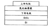
As aforesaid substrate, use formed thermal oxidation SiO on Si
2The substrate that the lower electrode film forming is arranged on the film surface.As this lower electrode, can use Pt, Ir, Rh, Ru, MgO, SrTiO
3, IrO
2, RuO
2, SrRuO
3, LaNiO
3Deng and so on, at the material of certain face direction orientation, and use Ir/SiO among the present invention
2/ Si, Pt/Ti/SiO
2/ Si and SRO/Pt/Ti/SiO
2/ Si.
As shown in Figure 2, on lower electrode, according to the thickness formation PZT strong dielectric oxide thin film of above-mentioned order with 100nm, in addition, for the electrical characteristic of the strong dielectric oxide thin film of gained PZT is estimated, adopt diameter 0.3mm mask to penetrate and sputter at the Pt film that forms on this film as upper electrode.In following embodiment, use this works to carry out various evaluations as sample.
Present embodiment is described about the inner wall surface that is arranged on the gas activation means between gas mixer and the jet tray dependence with respect to the pzt thin film characteristic.
Fig. 3 represents the inner wall surface area (m of gas activation means
2) with the leakage current density (A/m of pzt thin film when adding 1.5V
2) dependence.This occasion, the oxygen that flows to reative cell 2 is 91% with the ratio of aggregate supply gas.Substrate uses Ir (111) alignment films.Leakage current density is (interior surface area 0m when using gases activating means not
2) be 2.5E-6A/cm
2, inner wall surface area is 4.8E-3m
2The time be 2.0E-7, but reduce when increasing inner wall surface area, inner wall surface area is 2.1E-2m
2The time demonstrate minimum value 7.5E-8A/cm
2If increase inner wall surface area again, then leakage current density rises, and inner wall surface area is 5.2E-2m
2The time, be 1.7E-7A/cm
2
The dependence of polarization reversal charge density when Fig. 4 represents that the inner wall surface area of gas activation means and pzt thin film add 2.0V.This occasion, oxygen flow and substrate are same as described above.Polarization reversal charge density is 28 μ C/cm when using gases activating means not
2, inner wall surface area is 4.8E-3m
2The time be 39 μ C/cm
2If, increasing inner wall surface area then rise, inner wall surface area is 2.1E-2m
2The time, demonstrate maximum 48 μ C/cm
2If increase inner wall surface area again, then polarization reversal charge density descends, and inner wall surface area is 5.2E-2m
2The time be 40 μ C/cm
2
Fig. 5 represents the dependence of the polarization saturation voltage of the inner wall surface area of gas activation means and pzt thin film.This occasion, the flow and the substrate of oxygen are same as described above.The polarization saturation voltage is 2.2V when using gases activating means not, 4.8E-3m
2The time be 1.90V, if increase inner wall surface area then the saturation voltage that polarizes reduces, inner wall surface area is 2.1E-2m
2The time demonstrate minimum value 1.7V.If increase inner wall surface area again then the saturated density rising that polarizes, inner wall surface area is 5.2E-2m
2The time be 1.83V.
Though also do not get across clearly at present as above-mentioned, but estimate that this Organic Ingredients that the present invention uses resolves into tens of kinds intermediate and stable molecule (occasion of THF solvent resolves into intermediate or stable molecule more than or equal to 200 kinds) after all at least in its decomposable process.Can think that wherein the molecule of the containing metal atom of quite a few has the film forming of helping.The result of present embodiment demonstrates according to the molecule of the metallic atom that contains which catabolic phase is imported reative cell whether react membrane property (leakage current density, polarization reversal charge density, polarization saturation voltage) difference on substrate.
The inventor is for the catabolic phase of the molecule of getting the containing metal atom clear, carry out film forming expeditiously and improve membrane property, discovery must be in the unstripped gas that gasification obtains behind the mixed oxidization gas, if the gas activation means of control gas-phase decomposition state import reative cell to the molecule that becomes the containing metal atom that can obtain the good membrane property stage by jet tray.Embodiment 3
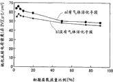
Present embodiment is described the dependence of relevant oxygen flow ratio and pzt thin film characteristic.
The dependence of the leakage current density when Fig. 6 represents in the mist that total oxygen flow ratio that imports the gas benchmark and pzt thin film add 1.5V.This occasion makes the oxygen flow ratio change 0.5~95%, and the inner wall surface area of gas activation means is set 2.1E-2m for
2, substrate uses Ir (111) alignment films.The oxygen flow ratio is 1% o'clock, and leakage current density is 1E-1, and along with the rising of oxygen flow ratio, leakage current density slowly reduces.
But as shown in Figure 7, among the XRD determining result of pzt thin film, (a) comparing among the figure, during oxygen flow ratio 80% (b among the figure), (111) orientation intensity significantly reduces with oxygen flow ratio 5%.The occasion of Fig. 7, Pb/ (Zr+Ti)=1.15.Fig. 8 represents the dependence of PZT (111) intensity of all orientations of pzt thin film in intensity of oxygen flow ratio and XRD determining.The oxygen flow ratio is changed 0.5~95% carries out.The ratio of XRD (111) intensity reduces with the increase of oxygen flow ratio.Therefore, illustrate that the reduction of leakage current density and epitaxial growth are in inner feelings (trade off) relation of tearing open.
Therefore, in the present embodiment, oxygen flow ratio in the gaseous mixture that uses in the initial stage layer film forming when changing nucleus and taking place (below, title initial stage layer oxygen flow ratio) (0.5~60%) is carried out epitaxial growth, and is made the film of the second layer of oxygen flow ratio 91% continuously.Research is shown in Fig. 9~14 to result of study with respect to the membrane property of the pzt thin film that makes like this.
Fig. 9 represents to sew when initial stage layer oxygen flow ratio and pzt thin film add 1.5V the dependence of current density.This occasion, the thickness of initial stage layer are 5nm, and the thickness of the second layer is 100nm.Leakage current density layer oxygen flow ratio in the early stage is 5% o'clock demonstration minimum value 2E-9, and the increase of layer oxygen flow ratio increases together along with the initial stage.Even find out that by Fig. 9 the oxygen flow ratio 0.5% leakage current density of initial stage layer is also very low, can obtain desired value up to less than about 60%, preferably to about 20%.
The dependence of polarization reversal charge density when Figure 10 represents that initial stage layer oxygen flow ratio and pzt thin film add 2.0V.Polarization reversal charge density layer oxygen flow ratio in the early stage is 5% o'clock demonstration maximum 66 μ C/cm
2Along with the increase of initial stage layer oxygen flow ratio reduce thereafter.Find out by Figure 10, even initial stage layer oxygen flow ratio 0.5% left and right sides polarization reversal charge density is also very high, can obtain desired value, preferably to about 20% up to less than about 60%.
Figure 11 represents the dependence of initial stage layer oxygen flow ratio and polarization saturation voltage.Polarization saturation voltage layer oxygen flow ratio in the early stage is 5% o'clock demonstration minimum value 1.29V, thereafter, reduces along with the increase of initial stage layer oxygen flow ratio.As seen from Figure 11, even initial stage layer oxygen flow ratio is about 0.5%, the polarization saturation voltage is also very low, can obtain desired value up to less than about 60%, preferably to about 20%.
Among Figure 12,13,14, the dependence of the leakage current density when adding 1.5V with regard to initial stage layer oxygen flow ratio and pzt thin film, the dependence of the polarization reversal charge density when adding 2.0V with pzt thin film, and with the polarization saturation voltage dependence, provided occasion (a among the figure, inner wall surface area 2.1E-2m that the gas activation means are arranged
2) and do not have the data of gas activation means occasion.Find out by these figure, the occasion of gas activation means is arranged if compare with the occasion that does not have the gas activation means, the oxygen flow ratio (0.5~95%) with respect to total can obtain low-leakage current density, high polarization reversal charge density and hypopolarization saturation voltage demonstrate excellent membrane property.
The initial stage layer Pb/ (Zr+Ti) that present embodiment is described formation initial stage nucleus form with the Pt substrate on the dependence of pzt thin film characteristic of film forming.This occasion, the inner wall surface area of the gas activation means between gas mixer one jet tray is set 2.08E-02m for
2, use Pt/Ti/SiO as substrate
2/ Si substrate.
At first, as the individual layer film forming, the oxygen flow ratio is 91% to be implemented as membrane process.Figure 15 represents the XRD determining result of gained pzt thin film.(film a) among Figure 15 does not observe the peak mutually relevant with the perovskite of PZT to Pb/ (Zr+Ti)=1.15, has only observed the pyrochlore phase.And the film of Pb/ (Zr+Ti)=1.80 (b among Figure 15), it is single-phase to have observed the PZT perovskite.Figure 16 represents that Pb/ (Zr+Ti) forms and the XRD intensity pyrochlore dependence of ratio mutually.Pb/ (Zr+Ti)=1.80 or when higher only observes the PZT orientation.But these PZT single phase film leakage current density is very big, can not obtain strong dielectric property.
Then, utilize the improvement that realizes characteristic as the continuous film forming of the initial stage layer of crystal seed layer and the second layer.Making the oxygen flow ratio is 5%, and making thickness is 5nm, changes the initial stage layer film forming that Pb/ (Zr+Ti) ratio of components forms the initial stage nucleus.On this initial stage layer, oxygen flow ratio 91%, the film of formation thickness 100nm.
Figure 17 represents that initial stage layer Pb/ (Zr+Ti) forms and the XRD intensity pyrochlore dependence of ratio mutually.Can infer by this figure, Pb/ (Zr+Ti)=1.69 or more Gao Shike to obtain PZT single-phase.
Figure 18 represents that initial stage layer Pb/ (Zr+Ti) forms and the dependence of polarization reversal charge density.Polarization reversal charge density increased with the increase that Pb/ (Zr+Ti) forms, and demonstrated maximum 52 μ C/cm at Pb/ (Zr+Ti)=1.75 o'clock
2Reduce at leisure greater than 1.75 o'clock polarization reversal charge density.
Figure 19 represents that initial stage layer Pb/ (Zr+Ti) forms and the dependence of polarization saturation voltage.The polarization saturation voltage reduces with the increase that Pb/ (Zr+Ti) forms, and shows at Pb/ (Zr+Ti)=1.75 o'clock to surpass minimum value 1.56V at 1.75 o'clock and rise at leisure.
Can infer that by these result can to obtain PZT between Pb/ (Zr+Ti)=1.69~1.82 single-phase, be mixed with the normal dielectric layer of PbO at Pb/ (Zr+Ti)=1.93 o'clock.
Present embodiment describe relevant initial stage layer Pb/ (Zr+Ti) form with at SrRuO
3(SRO) dependence of the pzt thin film characteristic of film forming on the substrate.
The SRO substrate confirms that also Pb is diffused among the SRO, and present embodiment also carries out the continuous film forming of the initial stage layer and the second layer, has studied the dependence of initial stage layer Pb/ (Zr+Ti) composition with the PZT membrane property.
Figure 20 represents that initial stage layer Pb/ (Zr+Ti) forms and the XRD intensity pyrochlore dependence of ratio mutually.This occasion is set in 2.08E-2m with the inner wall surface area of gas activation means
2, use SRO/Pt/Ti/SiO as substrate
2/ Si substrate.The oxygen flow ratio of initial stage during layer film forming is 91%, and the oxygen flow ratio during second layer film forming is 91% to carry out film forming.Find out significantly that by this figure pyrochlore phase ratio reduces with the increase that Pb/ (Zr+Ti) forms, become 0 at Pb/ (Zr+Ti)=1.31 or when higher.
Figure 21 represents that initial stage layer Pb/ (Zr+Ti) forms and the dependence of polarization reversal charge density.Plate counter-rotating charge density increases with the increase that Pb/ (Zr+Ti) forms, and demonstrates maximum 56 μ C/cm at Pb/ (Zr+Ti)=1.31 o'clock
2
Figure 22 represents that initial stage layer Pb/ (Zr+Ti) forms and the dependence of polarization saturation voltage.Polarization reversal voltage reduces with the increase that Pb/ (Zr+Ti) forms, and demonstrates minimum value 1.41V at Pb/ (Zr+Ti)=1.31 o'clock.
Found out that by Figure 20~22 it is single-phase to obtain PZT at Pb/ (Zr+Ti)=1.31 or when higher, membrane property also becomes desired value.But when thickness became the 100nm left and right sides, excessive Pb separated out in the grain boundary, estimated that leakage current density increases.In addition, as Figure 20~22, utilize rich Pb film by the initial stage layer, second layer minimizing Pb carries out continuous film forming and can reach purpose of the present invention.
Then, use the different pipe arrangement of internal diameter, make pzt thin film, its characteristic is compared according to the foregoing description as the gas activation means.Pipe arrangement internal diameter shown in the following table 1 is the pipe arrangement inner wall surface area of occasion of 10.2mm and 25mm and the relation of piping length.
(table 1)

Use apparatus for manufacturing thin film to make the occasion of pzt thin film as the gas activation means, flow into the oxygen of reative cell 2 and the ratio of aggregate supply gas (gaseous mixture) with above-mentioned pipe arrangement, with the occasion of Fig. 3 similarly be 91%.Figure 23 represents the gained pzt thin film, sews current density (A/cm when adding 1.5V as the inner wall surface area of the pipe arrangement of activating means
2) dependence.Clearly illustrate if inner wall surface area is identical by this figure, even then the different leakage current density of internal diameter also obtain roughly the same effect.
To with the above-mentioned pzt thin film that similarly makes, in Figure 24, express dependence, express among Figure 25 as the inner wall surface area of the pipe arrangement of gas activation means and the dependence of polarization saturation voltage as the inner wall surface area of the pipe arrangement of gas activation means polarization reversal charge density when adding 2.0V.By these figure clearly illustrate with the occasion of leakage current density similarly, if inner wall surface area is identical, even then the internal diameter difference also must cause roughly the same effect.
Industrial applicibility
Becoming the oxidizing gas flow proportional of setting partial pressure of oxygen according to the present invention by employing advances The row film forming, perhaps when reducing nucleus growth as the partial pressure of oxygen of the initial stage layer of crystal seed layer, then Oxidizing gas flow proportional when improving the film growth carries out continuous film forming, can realize promoting extension Growth, orientation is neat, and leakage current is few, the saturated strong dielectric of spontaneous polarization under the low-voltage Film. In addition, because will be at the metallic atom that contains of the stage decomposition that can obtain good membrane property Molecule import reative cell and can for the manufacture of strong dielectric film, obtain so can make oxygen defect The film that improves. Therefore, can provide the method for making the strong dielectric film that good film is arranged. In addition, by the gas activation means are set between gas mixer and jet tray, can provide The manufacturing installation of the improved film of oxygen defect. Therefore, this manufacture method and manufacturing installation exist Extremely useful in the manufacturing field of semiconductor devices.
Claims (11)
1. sull manufacture method, it is characterized in that with sull with material gasification unstripped gas, carrier gas and oxidizing gas in gas mixer, mix, supplying with the gaseous mixture that obtains by jet tray on being arranged at as the heated substrates in the reative cell of chemical vapor-phase growing apparatus reacts, on substrate, make in the method for sull, at first use this gaseous mixture film forming to be the initial stage layer as crystal seed layer, adopting the gaseous mixture continuous film forming with oxidizing gas flow proportional higher than initial stage layer occasion then is the second layer.
2. the described sull manufacture method of claim 1 is characterized in that, the oxidizing gas flow proportional in the film-forming process of this initial stage layer is a less than 60%, and the oxidizing gas flow proportional in the film-forming process of this second layer is more than or equal to 60%.
3. the described sull manufacture method of claim 1 is characterized in that, supplies with this gaseous mixture by the gas activation means that are arranged between blender and the jet tray in reative cell.
4. the described sull manufacture method of claim 3 is characterized in that, these gas activation means maintain the temperature of molecule that unstripped gas gas-phase decomposition when jet tray imports becomes to obtain the containing metal atom of desired membrane property.
5. the described sull manufacture method of claim 4 is characterized in that, the temperature that these gas activation means maintain the liquefaction that never produces unstripped gas, separate out is to the scope of the temperature that does not cause the unstripped gas film forming.
6. the described sull manufacture method of any one of claim 1~5 is characterized in that, as oxidizing gas, uses to be selected from oxygen, ozone, N
2O and NO
2Gas.
7. the described sull manufacture method of any one of claim 1~5 is characterized in that, as carrier gas, uses the inert gas that is selected from nitrogen, helium, argon, neon, krypton.
8. the described sull manufacture method of any one of claim 1~5 is characterized in that, as this substrate, uses to be selected from Pt, Ir, Rh, Ru, MgO, SrTiO
3, IrO
2, RuO
2, SrRuO
3And LaNiO
3The substrate of material system.
9. the described sull manufacture method of any one of claim 1~5 is characterized in that, as the sull raw material, uses to be selected from SiO
2, TiO
2, Al
2O
3, Ta
2O
5, MgO, ZrO
2, HfO
2, (Ba, Sr) TiO
2And SrTiO
3Normal dielectric oxide, be selected from Pb (Zr, Ti) O
3, SrBi
2Ta
2O
9And Bi
4Ti
3O
12Strong dielectric oxide.
10. the described sull manufacture method of any one of claim 1~5, it is characterized in that, the occasion that spreads in substrate easily by the atom of setting in the sull that makes manufacturing, the occasion that is difficult to be diffused into substrate than the amount of this atom in the initial stage layer is many, realizes epitaxial growth.
11. sull manufacturing installation, it is characterized in that with sull with material gasification unstripped gas, carrier gas and oxidizing gas mix in gas mixer, supplying with prepared gaseous mixture by jet tray on being arranged at as the heated substrates in the reative cell of chemical vapor-phase growing apparatus reacts, on substrate, make in the device of sull, the gas activation means are set between this blender and jet tray, and these gas activation means are the liquefaction that has not causing described unstrpped gas, separate out and the temperature of film forming under the pipe arrangement of the heater means that heats.
Applications Claiming Priority (2)
| Application Number | Priority Date | Filing Date | Title |
|---|---|---|---|
| JP2003300014 | 2003-08-25 | ||
| JP300014/2003 | 2003-08-25 |
Publications (2)
| Publication Number | Publication Date |
|---|---|
| CN1842901A CN1842901A (en) | 2006-10-04 |
| CN100435294C true CN100435294C (en) | 2008-11-19 |
Family
ID=34213796
Family Applications (1)
| Application Number | Title | Priority Date | Filing Date |
|---|---|---|---|
| CNB2004800243173A Active CN100435294C (en) | 2003-08-25 | 2004-08-25 | Process for producing oxide thin film and production apparatus therefor |
Country Status (7)
| Country | Link |
|---|---|
| US (1) | US20070054472A1 (en) |
| EP (1) | EP1662556B1 (en) |
| JP (1) | JP4628954B2 (en) |
| KR (2) | KR101246499B1 (en) |
| CN (1) | CN100435294C (en) |
| TW (1) | TW200511404A (en) |
| WO (1) | WO2005020311A1 (en) |
Families Citing this family (7)
| Publication number | Priority date | Publication date | Assignee | Title |
|---|---|---|---|---|
| JP2008053683A (en) * | 2006-07-27 | 2008-03-06 | Matsushita Electric Ind Co Ltd | Insulating film forming method, semiconductor device, and substrate processing apparatus |
| US20100000673A1 (en) * | 2006-08-02 | 2010-01-07 | Ulvac, Inc. | Film forming method and film forming apparatus |
| JP2010080813A (en) * | 2008-09-29 | 2010-04-08 | Fujifilm Corp | Piezoelectric film and method of manufacturing the same, piezoelectric device, and liquid discharge apparatus |
| TWI452946B (en) * | 2009-12-29 | 2014-09-11 | Univ Nat Yunlin Sci & Tech | Plasma reaction device |
| JP2014150191A (en) * | 2013-02-01 | 2014-08-21 | Ulvac Japan Ltd | Pzt film manufacturing method and deposition apparatus |
| CN106367732B (en) * | 2016-09-22 | 2018-11-06 | 四川大学 | A kind of medium temperature metal organic chemical vapor deposition TiO2-Al2O3Composite coating device and painting method |
| CN110586180B (en) * | 2019-09-20 | 2022-06-14 | 湖南师范大学 | Visible light catalysis N has2Preparation method of ruthenium hybrid deca-poly quaternary ammonium tungstate with O participating in selective oxidation |
Citations (5)
| Publication number | Priority date | Publication date | Assignee | Title |
|---|---|---|---|---|
| JPH0883793A (en) * | 1994-06-08 | 1996-03-26 | Hyundai Electron Ind Co Ltd | Formation of ferroelectric thin film |
| JPH08268797A (en) * | 1995-03-30 | 1996-10-15 | Hitachi Ltd | Chemical vapor phase reaction deposition device |
| JP2000058525A (en) * | 1998-08-03 | 2000-02-25 | Nec Corp | Vapor growth method for metal oxide dielectric film |
| US6090443A (en) * | 1997-07-18 | 2000-07-18 | Ramtron International Corporation | Multi-layer approach for optimizing ferroelectric film performance |
| US20030062554A1 (en) * | 2001-09-13 | 2003-04-03 | Atsushi Sakurai | Oriented ferroelectric thin-film device and method for manufacturing the same |
Family Cites Families (10)
| Publication number | Priority date | Publication date | Assignee | Title |
|---|---|---|---|---|
| JPH086181B2 (en) * | 1992-11-30 | 1996-01-24 | 日本電気株式会社 | Chemical vapor deposition method and chemical vapor deposition apparatus |
| US5989998A (en) * | 1996-08-29 | 1999-11-23 | Matsushita Electric Industrial Co., Ltd. | Method of forming interlayer insulating film |
| JPH1131650A (en) * | 1997-07-14 | 1999-02-02 | Kokusai Electric Co Ltd | Antireflection coating, substrate to be treated, manufacture of the substrate to be treated, manufacture of fine pattern and manufacture of semiconductor device |
| KR100392047B1 (en) * | 1998-12-16 | 2003-07-23 | 동경 엘렉트론 주식회사 | Method of forming thin film |
| US6495878B1 (en) * | 1999-08-02 | 2002-12-17 | Symetrix Corporation | Interlayer oxide containing thin films for high dielectric constant application |
| US6811651B2 (en) * | 2001-06-22 | 2004-11-02 | Tokyo Electron Limited | Gas temperature control for a plasma process |
| US20030012875A1 (en) * | 2001-07-10 | 2003-01-16 | Shreyas Kher | CVD BST film composition and property control with thickness below 200 A for DRAM capacitor application with size at 0.1mum or below |
| US6713127B2 (en) * | 2001-12-28 | 2004-03-30 | Applied Materials, Inc. | Methods for silicon oxide and oxynitride deposition using single wafer low pressure CVD |
| JP3971645B2 (en) * | 2002-04-30 | 2007-09-05 | 富士通株式会社 | Manufacturing method of semiconductor device |
| US6884464B2 (en) * | 2002-11-04 | 2005-04-26 | Applied Materials, Inc. | Methods for forming silicon comprising films using hexachlorodisilane in a single-wafer deposion chamber |
-
2004
- 2004-08-25 KR KR1020117021973A patent/KR101246499B1/en active IP Right Grant
- 2004-08-25 JP JP2005513346A patent/JP4628954B2/en active Active
- 2004-08-25 US US10/569,470 patent/US20070054472A1/en not_active Abandoned
- 2004-08-25 WO PCT/JP2004/012180 patent/WO2005020311A1/en active Application Filing
- 2004-08-25 KR KR1020067003747A patent/KR101179098B1/en active IP Right Grant
- 2004-08-25 CN CNB2004800243173A patent/CN100435294C/en active Active
- 2004-08-25 EP EP04772141.0A patent/EP1662556B1/en active Active
- 2004-08-26 TW TW093125554A patent/TW200511404A/en unknown
Patent Citations (5)
| Publication number | Priority date | Publication date | Assignee | Title |
|---|---|---|---|---|
| JPH0883793A (en) * | 1994-06-08 | 1996-03-26 | Hyundai Electron Ind Co Ltd | Formation of ferroelectric thin film |
| JPH08268797A (en) * | 1995-03-30 | 1996-10-15 | Hitachi Ltd | Chemical vapor phase reaction deposition device |
| US6090443A (en) * | 1997-07-18 | 2000-07-18 | Ramtron International Corporation | Multi-layer approach for optimizing ferroelectric film performance |
| JP2000058525A (en) * | 1998-08-03 | 2000-02-25 | Nec Corp | Vapor growth method for metal oxide dielectric film |
| US20030062554A1 (en) * | 2001-09-13 | 2003-04-03 | Atsushi Sakurai | Oriented ferroelectric thin-film device and method for manufacturing the same |
Also Published As
| Publication number | Publication date |
|---|---|
| EP1662556B1 (en) | 2013-11-06 |
| TW200511404A (en) | 2005-03-16 |
| JPWO2005020311A1 (en) | 2007-11-01 |
| JP4628954B2 (en) | 2011-02-09 |
| CN1842901A (en) | 2006-10-04 |
| KR101246499B1 (en) | 2013-03-25 |
| EP1662556A4 (en) | 2012-05-09 |
| KR101179098B1 (en) | 2012-09-03 |
| TWI363377B (en) | 2012-05-01 |
| KR20110116065A (en) | 2011-10-24 |
| KR20060118418A (en) | 2006-11-23 |
| EP1662556A1 (en) | 2006-05-31 |
| WO2005020311A1 (en) | 2005-03-03 |
| US20070054472A1 (en) | 2007-03-08 |
Similar Documents
| Publication | Publication Date | Title |
|---|---|---|
| KR100300834B1 (en) | Cvd apparatus for and method of forming thin film having high dielectric constant | |
| KR100269851B1 (en) | Manufacturing method of semiconductor device | |
| JP3462852B2 (en) | Method and apparatus for producing thin films by chemical vapor deposition | |
| KR100418461B1 (en) | Process for metal metalloid oxides and nitrides with compositional gradients | |
| CN101048853B (en) | Precursor for film formation and method for forming ruthenium-containing film | |
| JP3576934B2 (en) | Method for growing multimetallic compound layers and compositions for growing mixed metal or metal compound layers | |
| US6787186B1 (en) | Method of controlled chemical vapor deposition of a metal oxide ceramic layer | |
| JPWO2012039107A1 (en) | Thin film manufacturing method and thin film manufacturing apparatus | |
| TW201139721A (en) | Thin film manufacturing apparatus, thin film manufacturing method, and method for manufacturing semiconductor device | |
| US20030080325A1 (en) | Chemical vapor deposition method of making layered superlattice materials using trimethylbismuth | |
| KR100322821B1 (en) | Semiconductor device and its manufacturing method | |
| TW527665B (en) | Chemical vapor deposition process for fabricating layered superlattice materials | |
| CN100435294C (en) | Process for producing oxide thin film and production apparatus therefor | |
| JPH11317377A (en) | Cvd material for forming electrodes and capacitor electrodes and wiring film formed with the same | |
| US20040209384A1 (en) | Low temperature chemical vapor deposition process for forming bismuth-containing ceramic thin films useful in ferroelectric memory devices | |
| JPH08176826A (en) | Thin film depositing device by cvd, deposition method and cvd material and liquid material vessel used in the device or method | |
| KR20030014659A (en) | FORMING FERROELECTRIC Pb(Zr,Ti)O3 FILMS | |
| CN101116183A (en) | Method for manufacturing capacity element, method for manufacturing semiconductor device and semiconductor-manufacturing apparatus | |
| US7629183B2 (en) | Method for manufacturing semiconductor device and computer storage medium | |
| WO2000008680A1 (en) | Vapor growth method for metal oxide dielectric film and vapor growth device for metal oxide dielectric material | |
| Jung et al. | Strontium ruthenium oxide deposition in supercritical carbon dioxide using a closed reactor system | |
| JP4205565B2 (en) | Thin film manufacturing method | |
| US20050167713A1 (en) | Ferroelectric capacitor and method of production of same | |
| JPH09241849A (en) | Apparatus for production of oxide thin film and its production | |
| JP2003142473A (en) | Gas supplying apparatus and method therefor, and film forming apparatus and method therefor |
Legal Events
| Date | Code | Title | Description |
|---|---|---|---|
| C06 | Publication | ||
| PB01 | Publication | ||
| C10 | Entry into substantive examination | ||
| SE01 | Entry into force of request for substantive examination | ||
| C14 | Grant of patent or utility model | ||
| GR01 | Patent grant |