JP4205565B2 - Thin film manufacturing method - Google Patents
Thin film manufacturing method Download PDFInfo
- Publication number
- JP4205565B2 JP4205565B2 JP2003403975A JP2003403975A JP4205565B2 JP 4205565 B2 JP4205565 B2 JP 4205565B2 JP 2003403975 A JP2003403975 A JP 2003403975A JP 2003403975 A JP2003403975 A JP 2003403975A JP 4205565 B2 JP4205565 B2 JP 4205565B2
- Authority
- JP
- Japan
- Prior art keywords
- thin film
- gas
- temperature
- film
- film manufacturing
- Prior art date
- Legal status (The legal status is an assumption and is not a legal conclusion. Google has not performed a legal analysis and makes no representation as to the accuracy of the status listed.)
- Expired - Lifetime
Links
- 239000010409 thin film Substances 0.000 title claims description 88
- 238000004519 manufacturing process Methods 0.000 title claims description 26
- 239000010408 film Substances 0.000 claims description 90
- 239000007789 gas Substances 0.000 claims description 74
- 239000000758 substrate Substances 0.000 claims description 44
- 230000015572 biosynthetic process Effects 0.000 claims description 41
- 239000002994 raw material Substances 0.000 claims description 41
- 238000000137 annealing Methods 0.000 claims description 38
- 238000006243 chemical reaction Methods 0.000 claims description 36
- 239000007788 liquid Substances 0.000 claims description 33
- 238000002425 crystallisation Methods 0.000 claims description 31
- 230000008025 crystallization Effects 0.000 claims description 31
- 230000008016 vaporization Effects 0.000 claims description 26
- 238000009834 vaporization Methods 0.000 claims description 23
- 239000002904 solvent Substances 0.000 claims description 16
- 238000000151 deposition Methods 0.000 claims description 15
- 230000008021 deposition Effects 0.000 claims description 13
- XDTMQSROBMDMFD-UHFFFAOYSA-N Cyclohexane Chemical compound C1CCCCC1 XDTMQSROBMDMFD-UHFFFAOYSA-N 0.000 claims description 9
- 238000000034 method Methods 0.000 claims description 9
- 230000008569 process Effects 0.000 claims description 6
- 239000012495 reaction gas Substances 0.000 claims description 6
- 238000011084 recovery Methods 0.000 claims description 6
- 238000000354 decomposition reaction Methods 0.000 claims description 5
- 229910004298 SiO 2 Inorganic materials 0.000 claims description 3
- 238000001556 precipitation Methods 0.000 claims description 3
- 238000005245 sintering Methods 0.000 claims 1
- 239000006200 vaporizer Substances 0.000 description 19
- 239000002245 particle Substances 0.000 description 18
- 239000003990 capacitor Substances 0.000 description 17
- 230000010287 polarization Effects 0.000 description 14
- 238000005229 chemical vapour deposition Methods 0.000 description 13
- 238000002441 X-ray diffraction Methods 0.000 description 9
- 239000000203 mixture Substances 0.000 description 8
- 239000000463 material Substances 0.000 description 7
- IJGRMHOSHXDMSA-UHFFFAOYSA-N Atomic nitrogen Chemical compound N#N IJGRMHOSHXDMSA-UHFFFAOYSA-N 0.000 description 6
- 238000001228 spectrum Methods 0.000 description 6
- 238000010438 heat treatment Methods 0.000 description 5
- 230000001590 oxidative effect Effects 0.000 description 5
- 239000012159 carrier gas Substances 0.000 description 4
- 238000002488 metal-organic chemical vapour deposition Methods 0.000 description 4
- 239000004065 semiconductor Substances 0.000 description 4
- QVGXLLKOCUKJST-UHFFFAOYSA-N atomic oxygen Chemical compound [O] QVGXLLKOCUKJST-UHFFFAOYSA-N 0.000 description 3
- 230000001276 controlling effect Effects 0.000 description 3
- 239000011261 inert gas Substances 0.000 description 3
- 238000002156 mixing Methods 0.000 description 3
- 229910052757 nitrogen Inorganic materials 0.000 description 3
- 239000001301 oxygen Substances 0.000 description 3
- 229910052760 oxygen Inorganic materials 0.000 description 3
- 239000000654 additive Substances 0.000 description 2
- 230000000996 additive effect Effects 0.000 description 2
- 239000013078 crystal Substances 0.000 description 2
- 238000010586 diagram Methods 0.000 description 2
- 229910052746 lanthanum Inorganic materials 0.000 description 2
- 238000012423 maintenance Methods 0.000 description 2
- 230000001105 regulatory effect Effects 0.000 description 2
- 229910018072 Al 2 O 3 Inorganic materials 0.000 description 1
- MYMOFIZGZYHOMD-UHFFFAOYSA-N Dioxygen Chemical compound O=O MYMOFIZGZYHOMD-UHFFFAOYSA-N 0.000 description 1
- 241000877463 Lanio Species 0.000 description 1
- XUIMIQQOPSSXEZ-UHFFFAOYSA-N Silicon Chemical compound [Si] XUIMIQQOPSSXEZ-UHFFFAOYSA-N 0.000 description 1
- 229910004121 SrRuO Inorganic materials 0.000 description 1
- 229910002367 SrTiO Inorganic materials 0.000 description 1
- ATJFFYVFTNAWJD-UHFFFAOYSA-N Tin Chemical compound [Sn] ATJFFYVFTNAWJD-UHFFFAOYSA-N 0.000 description 1
- 230000002411 adverse Effects 0.000 description 1
- 238000004458 analytical method Methods 0.000 description 1
- 230000004888 barrier function Effects 0.000 description 1
- 239000006227 byproduct Substances 0.000 description 1
- 230000008859 change Effects 0.000 description 1
- 230000007423 decrease Effects 0.000 description 1
- 230000007547 defect Effects 0.000 description 1
- 230000002950 deficient Effects 0.000 description 1
- 238000009792 diffusion process Methods 0.000 description 1
- 238000010790 dilution Methods 0.000 description 1
- 239000012895 dilution Substances 0.000 description 1
- 229910001882 dioxygen Inorganic materials 0.000 description 1
- 239000000428 dust Substances 0.000 description 1
- 230000000694 effects Effects 0.000 description 1
- 239000007772 electrode material Substances 0.000 description 1
- 238000001704 evaporation Methods 0.000 description 1
- 230000008020 evaporation Effects 0.000 description 1
- 230000005294 ferromagnetic effect Effects 0.000 description 1
- 230000006870 function Effects 0.000 description 1
- 239000001307 helium Substances 0.000 description 1
- 229910052734 helium Inorganic materials 0.000 description 1
- SWQJXJOGLNCZEY-UHFFFAOYSA-N helium atom Chemical compound [He] SWQJXJOGLNCZEY-UHFFFAOYSA-N 0.000 description 1
- UCNNJGDEJXIUCC-UHFFFAOYSA-L hydroxy(oxo)iron;iron Chemical compound [Fe].O[Fe]=O.O[Fe]=O UCNNJGDEJXIUCC-UHFFFAOYSA-L 0.000 description 1
- 230000010354 integration Effects 0.000 description 1
- 229910052741 iridium Inorganic materials 0.000 description 1
- 230000015654 memory Effects 0.000 description 1
- 239000002184 metal Substances 0.000 description 1
- 229910052751 metal Inorganic materials 0.000 description 1
- 239000003921 oil Substances 0.000 description 1
- 239000003960 organic solvent Substances 0.000 description 1
- 150000002902 organometallic compounds Chemical class 0.000 description 1
- 239000007800 oxidant agent Substances 0.000 description 1
- 229910052697 platinum Inorganic materials 0.000 description 1
- WQGWDDDVZFFDIG-UHFFFAOYSA-N pyrogallol Chemical compound OC1=CC=CC(O)=C1O WQGWDDDVZFFDIG-UHFFFAOYSA-N 0.000 description 1
- 239000000376 reactant Substances 0.000 description 1
- 238000001953 recrystallisation Methods 0.000 description 1
- 230000009467 reduction Effects 0.000 description 1
- 229910052707 ruthenium Inorganic materials 0.000 description 1
- 229910052710 silicon Inorganic materials 0.000 description 1
- 239000010703 silicon Substances 0.000 description 1
- 239000007787 solid Substances 0.000 description 1
- 239000000243 solution Substances 0.000 description 1
- 229910001220 stainless steel Inorganic materials 0.000 description 1
- 239000010935 stainless steel Substances 0.000 description 1
- 239000000126 substance Substances 0.000 description 1
- 238000003852 thin film production method Methods 0.000 description 1
- 229910052726 zirconium Inorganic materials 0.000 description 1
Images


Description
本発明は、薄膜製造方法に関し、特に、MOCVD等のCVD法により酸化物薄膜を製造する方法に関する。 The present invention relates to a thin film manufacturing method, and more particularly to a method of manufacturing an oxide thin film by a CVD method such as MOCVD.
近年、半導体分野では、半導体素子の高集積化、高性能化が求められている。これらの要求を解決するための手段として、段差被覆性に優れ、欠陥の少ない緻密な膜が期待されるCVD(化学気相成長)法による成膜が注目を集めている。 In recent years, high integration and high performance of semiconductor elements are required in the semiconductor field. As means for solving these demands, film formation by CVD (chemical vapor deposition) method, which is expected to be a dense film having excellent step coverage and few defects, has attracted attention.
また、これらの要求に応えるために、新材料の導入も提案されている。この新材料の導入の際の問題を解決したり、また、元素の拡散などの問題を解決するためには、成膜プロセス温度のなお一層の低温化が要求されている。 In order to meet these requirements, the introduction of new materials has also been proposed. In order to solve the problems at the time of introducing this new material and to solve problems such as element diffusion, it is required to further lower the film forming process temperature.
また、Ta2O5、(Ba,Sr)TiO3、SrTiO3などの高誘電率誘電体酸化物、Pb(Zr,Ti)O3、SrBi2Ta2O9、Bi4Ti3O12などの強誘電体酸化物、IrO2、RuO2、SrRuO3、LaNiO3などの電気伝導性酸化物、(La,Sr)MnO3、(Pr,Ca)MnO3などの強磁性酸化物からなる薄膜は、高集積化素子、低消費電力化素子、不揮発メモリー、キャパシターの電極材などといった利用用途から注目を集めている。しかし、これらの膜を低温で成膜すると、膜が結晶化せず、各用途として機能する状態にならないこと、下地との界面付近の膜組成が異なること、大きなリーク電流が発生することなどの種々の問題が発生する。例えば、膜中の酸素が欠損して、良好なエピタキシャル成長が妨げられると、常誘電体酸化物膜及び強誘電体酸化物膜では絶縁性がそれぞれ低下し、また、電気伝導性酸化物膜及び強磁性酸化物膜では電気伝導性がそれぞれ低下するという問題がある。
Also, high dielectric constant dielectric oxides such as Ta 2 O 5 , (Ba, Sr) TiO 3 , SrTiO 3 , Pb (Zr, Ti) O 3 , SrBi 2 Ta 2 O 9 , Bi 4 Ti 3 O 12, etc. ferroelectric oxide, IrO 2, RuO 2, SrRuO 3, electrically conductive oxides such as LaNiO 3, (La, Sr)
本発明の課題は、上記従来技術の問題点に鑑み、低温でCVD法により薄膜を製造する際に、成膜初期の膜組成のずれを補正し、膜厚方向に組成を制御することにより、電気特性に優れた、特にリーク電流密度が2V印加で1.0E−3A/cm2以下であり、かつ分極反転電荷密度が2V印加で25μC/cm2以上である薄膜を製造する方法を提供することにある。 The problem of the present invention is to solve the above-mentioned problems of the prior art, by correcting a film composition deviation at the initial stage of film formation and controlling the composition in the film thickness direction when manufacturing a thin film by a CVD method at a low temperature, Provided is a method for producing a thin film having excellent electrical characteristics, in particular, a leakage current density of 1.0E-3 A / cm 2 or less when 2 V is applied and a polarization reversal charge density of 25 μC / cm 2 or more when 2 V is applied. There is.
請求項1によれば、本発明の薄膜製造方法は、Pb(thd) 2 、Zr(dmhd) 4 及びTi(i−PrO) 2 (thd) 2 を溶媒に溶かした液体を気化システムを用いて気化した原料ガスと反応ガスとを含む成膜ガスをガス導入手段を介して反応室内に導入し、原料ガスの分解温度以上に加熱された基板上にPZT薄膜を成膜する薄膜製造方法において、上記Pb(thd) 2 を溶媒に溶かした液体、上記Zr(dmhd) 4 を溶媒に溶かした液体、上記Ti(i−PrO) 2 (thd) 2 を溶媒に溶かした液体を所定の流量で上記気化システムに供給することで、上記基板上に初期層を成膜した後、上記Pb(thd) 2 を溶媒に溶かした液体の流量を上記初期層の成膜時の流量よりも少なくして、上記初期層の上にバルク層を成膜することを特徴とする。
According to
上記したような配合割合の成膜ガスを用いて初期層及びバルク層からなるPZT薄膜を製造することにより、結晶化が促進された薄膜であって、電気特性の優れた薄膜、例えば、低いリーク電流密度、高い分極反転電荷密度を有し、また、その電荷密度の低電圧での立ち上がりが良好である薄膜を得ることができる。例えば、2V印加で1.0E−3A/cm2以下、好ましくは1.0E−4/cm2以下のリーク電流密度、また、2V印加で25μC/cm2以上、好ましくは30μC/cm2以上の分極反転電荷密度を有する薄膜を得ることができる。さらに、PZT薄膜の配向方向に基板の配向方向を反映させることができる。 By manufacturing a PZT thin film composed of an initial layer and a bulk layer using a film forming gas having a blending ratio as described above, the thin film has improved crystallization and has excellent electrical characteristics, for example, low leakage. A thin film having a current density, a high polarization inversion charge density, and a good rise of the charge density at a low voltage can be obtained. For example, 1.0E-3A / cm 2 or less at 2V applied, preferably 1.0E-4 / cm 2 or less of the leakage current density also,, 25μC / cm 2 or more at 2V applied, preferably 30 .mu.C / cm 2 or more A thin film having a polarization reversal charge density can be obtained. Furthermore, the orientation direction of the substrate can be reflected in the orientation direction of the PZT thin film.
請求項2によれば、上記気化システムから反応室上部のガス導入手段内までの経路の温度を、該原料ガスが基板へ到達する前に析出又は分解を起こすことのない温度に設定して前記初期層及びバルク層を成膜することを特徴とする。
原料ガス組成に応じて経路等の温度を適宜設定することにより、パーティクルの発生が防止され、所望の電気特性を有する薄膜を製造できる。
According to
By appropriately setting the temperature of the path or the like according to the raw material gas composition, generation of particles can be prevented and a thin film having desired electrical characteristics can be manufactured.
請求項3によれば、上記バルク層を成膜した後、上記バルク層の成膜温度以下の温度で結晶化アニール処理を行うことを特徴とする。
According to
上記した温度範囲で結晶化アニール処理することにより、結晶化が促進された薄膜であって、電気特性の優れた薄膜、例えば、低いリーク電流密度や高い分極反転電荷密度を有する薄膜を得ることができる。 By performing the crystallization annealing treatment in the above-mentioned temperature range, it is possible to obtain a thin film with accelerated crystallization and excellent electrical characteristics, for example, a thin film having a low leakage current density and a high polarization inversion charge density. it can.
請求項4によれば、上記結晶化アニール処理の後に、上記バルク層の上に上部電極を成膜し、上記上部電極の成膜時のダメージを回復させる回復アニール処理を、上記結晶化アニール処理と同じ条件で行うことを特徴とする。この回復アニール処理により、上部電極成膜時の下地膜へのダメージが回復される。 According to the fourth aspect of the present invention , after the crystallization annealing treatment , a recovery annealing treatment for forming an upper electrode on the bulk layer and recovering damage at the time of film formation of the upper electrode is performed by the crystallization annealing treatment. and wherein the line Ukoto under the same conditions as. By this recovery annealing treatment, damage to the base film during upper electrode film formation is recovered.
請求項5によれば、上記初期層の厚さが上記バルク層の厚さよりも薄いことを特徴とする。これにより、電気特性の優れた薄膜を得ることができる。
請求項6によれば、上記初期層の厚さが上記バルク層の厚さの20分の1以下であることを特徴とする。
請求項7によれば、上記初期層の厚さが2nm以上20nm以下であることを特徴とする。
初期層の厚さを上記したような厚さにすることにより、低いリーク電流密度、高い分極反転電荷密度を有する薄膜を製造できる。
According to
According to claim 6, the thickness of the initial layer is characterized by one less der Rukoto twentieth of the thickness of the bulk layer.
According to
By setting the thickness of the initial layer as described above, a thin film having a low leakage current density and a high polarization inversion charge density can be manufactured.
請求項8によれば、上記溶媒がシクロヘキサンであることを特徴とする。
According to
請求項9によれば、上記基板がIr電極付きSiO2/Si基板であることを特徴とする。 According to claim 9, said substrate and said SiO 2 / Si substrate der Rukoto with Ir electrode.
本発明によれば、所定の配合割合の原料ガスを有する成膜ガスを用いて、成膜初期の組成ずれを補正し、膜厚方向に組成を制御することにより、また、成膜後に所定の条件でアニール処理を行うことにより、結晶化が促進された薄膜であって、電気特性の優れた薄膜、例えば、低いリーク電流密度、高い分極反転電荷密度を有し、その電荷密度の低電圧での立ち上がりが良好である薄膜を得ることができるという効果が達成される。 According to the present invention, by using a film-forming gas having a raw material gas with a predetermined blending ratio, correcting a composition shift at the initial stage of film formation and controlling the composition in the film thickness direction, and after film formation, A thin film whose crystallization is promoted by annealing treatment under conditions, and has excellent electrical characteristics, for example, a low leakage current density, a high polarization inversion charge density, and a low voltage of the charge density. The effect that a thin film having a good rise can be obtained.
以下、本発明に係わる薄膜製造方法を実施するための装置の一例として、図1に示すCVD薄膜製造装置の概略の配置・構成図を参照して説明する。 Hereinafter, an example of an apparatus for carrying out the thin film manufacturing method according to the present invention will be described with reference to a schematic arrangement / configuration diagram of a CVD thin film manufacturing apparatus shown in FIG.
図1に示すCVD薄膜製造装置は、真空排気システム1に圧力調整バルブ1aを介して接続された反応室2と、反応室の上部に設けられたガス導入手段としてのシャワープレート3に所定の長さの成膜ガス配管4により接続されたガス混合器5と、この混合器5に原料ガス配管6により接続された気化システムである気化器7とを有している。
The CVD thin film manufacturing apparatus shown in FIG. 1 has a
気化器7から反応室2までのガス配管・各種バルブ・混合器等を含む装置構成物には気化した原料ガスが液化/析出/成膜しない温度に保つために、ヒータ等の加熱手段や熱交換器が設けられている。気化器7と混合器5との間の配管6にはバルブV1が、また、気化器7と排気システム1との間の配管8にはバルブV2が設けられ、これにより気化器7、混合器5、排気システム1を遮断できるように構成されている。これは、気化器7、混合器5及び排気システム1の構成要素の各々のメンテナンスサイクルが異なるため、大気開放により成膜に悪影響を及ぼす水分等の物質がこれら構成要素に付着するのを避けることが目的である。1つの構成要素を大気開放してメンテナンスしている場合に、他の2つの構成要素をも大気開放することなく、真空を保持しうるように構成されている。
In order to keep the vaporized source gas at a temperature at which the vaporized source gas is not liquefied / deposited / deposited on the apparatus components including the gas piping from the
以下、上記各構成要素について詳細に説明する。
反応室2には、成膜対象物である基板Sを載置するための、基板加熱手段を有する基板ステージ2−1が配設されており、この加熱された基板上にシャワープレート3から成膜ガスが導入される。基板Sとの反応に使用されなかった余剰の成膜ガスや、基板との反応により生じた成膜ガスとの副生成物ガスや、反応物ガスが排気システム1により排気される。シャワープレート3は適度に加熱され、導入ガスが液化/析出/成膜しない温度に保たれている。
Hereafter, each said component is demonstrated in detail.
The
この反応室2の上部に設けられたシャワープレート3には、成膜ガス中に存在するパーティクルを捕獲するためのフィルターとしてのパーティクル捕獲器が配設されていてもよい。このパーティクル捕獲器は、シャワープレートのシャワーホール直前に設けられていても良く、反応に必要な特定の気化した原料元素を付着・捕獲しない温度に適切に調整されていることが望ましい。
The
上記排気システム1と反応室2との間に設けられた圧力調整バルブ1aにより、様々な成膜圧力条件に容易に対応することが出来る。
Various film forming pressure conditions can be easily accommodated by the
混合器5は、バルブV1が設けられている配管6により気化器7に接続されると共に、バルブ、熱交換器、マスフローコントローラ(図示せず)を介してそれぞれ二つのガス源(例えば、酸素などの酸化ガス源:窒素などの不活性ガスである希釈ガス源)にも連結されている。混合器5内で均一に混合されて得られた成膜ガスは、配管4を経てシャワープレート3を介して反応室2へ導入され、室内において層流になることなく基板ステージ2−1上に載置された成膜対象物表面に供給される。
The
混合器5では、酸化ガス源から供給される適度に加熱された酸化ガスと、気化器7により生じ、液化/析出/成膜しない温度に保たれた配管6を経て送られる原料ガスとが導入・混合され、成膜ガス(酸化ガス+原料ガス)が得られる。この原料ガスは、1種類の又は複数の種類のガスが混じったガスである。かくして得られた成膜ガスは、配管4を経て反応室2内に導入される。
In the
この配管4及び6はVCR継手で接続されていてもよく、一部の配管各継手のVCRガスケットは、ただのリングではなく穴のところがパーティクル捕獲器となっているVCR型パーティクル捕獲器であっても良い。このVCR型パーティクル捕獲器のある継手部は、原料ガスが液化/析出しない温度よりも高く設定・保持され、かつ、反応に必要な特定の気化した原料元素を付着・捕獲しないようにすることが望ましい。
These
ガス混合器5とシャワープレート3との間の成膜ガス配管4には、成膜ガスの切替えを行うバルブが混合器5の2次側に設けてあってもよい。このバルブの下流側は、反応室2に接続されている。成膜時は、このバルブを開け、成膜終了後にこのバルブを閉じる。
In the film forming
気化器7には、原料供給部7aと気化部(図示せず)とが接続されている。この気化器は、加圧ガス(例えば、Heガス等の不活性ガス)により液体・固体原料を有機溶媒に溶解した原料液A、B、Cを加圧・搬送し、圧送された原料液のそれぞれの流量を各液体流量制御器で制御して、キャリアガスにより気化部に運ぶように構成されている。
A raw
気化部は、流量の制御された原料液を効率よく気化させ、気化して得られた原料ガスを混合器5へ供給することができるように構成されている。この気化部では、液体原料が1種の場合は単液を、液体原料が複数の場合は複数の原料液を混合して気化させることができる。原料液を気化させる際は、原料液の液滴を気化させるだけでなく、液滴にガスを当てたり、物理的な振動を与えたり又は超音波を当てたりして、気化部の壁面に設けたノズルを介して更に細かい液粒として気化部内に導入して気化させ、気化効率を上げることが好ましい。気化部の内部には、液滴又は液粒が、効率良く気化すべき箇所で極力気化することができるように、かつ、各種パーティクル捕獲器による液粒気化負荷の軽減のために、Al等の熱伝導の良い材料で作製された気化部材が配置されることが好ましい。
The vaporizing section is configured to efficiently vaporize the raw material liquid whose flow rate is controlled and supply the raw material gas obtained by the vaporization to the
また、気化部の内部には、原料液が気化する際に発生する残渣を元とするパーティクルを気化部外に出さないようにするために、また、少量流れ来る液滴が気化器外に真空により吸い込まれることなく気化できるようにするために、パーティクル捕獲器を設けてもよい。この気化部材とパーティクル捕獲器においては、これらに接触した液滴、細かい液粒が確実に気化できるように、かつ、反応に必要な特定の気化した原料元素を付着・捕獲しないように、適切な温度に気化条件が保たれていることが望ましい。 In addition, in order to prevent particles based on the residue generated when the raw material liquid is vaporized from exiting the vaporizer, a small amount of liquid droplets are vacuumed outside the vaporizer. In order to be able to vaporize without being sucked by a particle trap, a particle trap may be provided. In this vaporization member and particle trap, appropriate droplets and fine liquid droplets that come into contact with these vaporization members and fine liquid particles can be surely vaporized, and appropriate vaporization source elements necessary for the reaction should not be attached and captured. It is desirable that vaporization conditions be maintained at the temperature.
なお、この気化器7は、原料溶解用の溶媒Dを有し、その流量を流量制御器で制御して気化部へ導入して気化部で気化させ、この溶媒ガスを作ることが可能なように構成されていてもよい。この溶媒ガスを用いて装置内部をクリーニングできる。
The
上記したように、本発明で用いる薄膜製造装置は、好ましくは円筒形状の反応室2を有しており、この反応室の内部には、シリコンウェハー等の基板が載置される円筒形状の基板ステージ2−1が設けられている。この基板ステージには、基板を加熱するための加熱手段が組み込まれている。また、反応室2は、基板ステージ2−1を反応室の成膜位置と反応室下方の基板搬送位置との間で昇降自在に構成するための手段を備えていてもよい。反応室2上側の中央部には、基板ステージ2−1に対向してシャワープレート3が設けられ、パーティクルの除去された成膜ガスがシャワープレート3から基板の中央部に向かって噴出されるように構成されている。
As described above, the thin film manufacturing apparatus used in the present invention preferably has a
ところで、MOCVD法等のCVD法により基板上に薄膜を製造する場合、原料ガスがある温度以下に低下すると、原料ガスがパーティクルとして析出し、反応室内での成膜ダストの原因ともなる。そのため、酸化ガス用配管にガス温度調節手段である熱交換器を設けたり、また、原料ガスの析出を防止するために反応室2の外壁や基板ステージ2−1にヒータ等の加熱手段を設けてある。
Incidentally, when a thin film is produced on a substrate by a CVD method such as the MOCVD method, when the source gas is lowered below a certain temperature, the source gas is precipitated as particles, which may cause film formation dust in the reaction chamber. Therefore, a heat exchanger as a gas temperature adjusting means is provided in the oxidizing gas pipe, and a heating means such as a heater is provided on the outer wall of the
本発明の薄膜製造方法を実施する際の成膜温度は、特に制限される訳ではなく、MOCVD法等のCVD法における既知の成膜温度であればよい。例えば、550℃程度以下、好ましくは450〜550℃程度の成膜温度であればよい。本発明では、2層以上の層からなる薄膜を製造し、また、所定の温度で結晶化アニール処理を行うことにより所期の目的を達成しているため、これよりさらに低い成膜温度によるプロセスでも実施できる。 The film formation temperature at the time of carrying out the thin film production method of the present invention is not particularly limited, and may be a known film formation temperature in a CVD method such as the MOCVD method. For example, the film forming temperature may be about 550 ° C. or less, preferably about 450 to 550 ° C. In the present invention, a thin film composed of two or more layers is manufactured, and the intended purpose is achieved by performing a crystallization annealing treatment at a predetermined temperature. But it can be done.
また、本発明におけるこの結晶化アニール処理は、成膜温度以下の温度で実施すればよい。例えば、成膜温度が530℃の場合、成膜温度より110℃低い温度、好ましくは80℃低い温度、さらに好ましくは50℃低い温度から成膜温度付近までの間の温度で結晶化アニール処理を実施すれば、満足すべき結晶化が得られると共に、所望の電気特性を有する薄膜が得られる。 Further, this crystallization annealing treatment in the present invention may be performed at a temperature lower than the film forming temperature. For example, when the film formation temperature is 530 ° C., the crystallization annealing treatment is performed at a temperature 110 ° C. lower than the film formation temperature, preferably 80 ° C., more preferably 50 ° C. to a temperature near the film formation temperature. When carried out, satisfactory crystallization is obtained and a thin film having desired electrical characteristics is obtained.
上記した図1に示す薄膜製造装置を用いれば、原料源としてPt、Ir、Ru等を含む有機金属化合物を用いたキャパシタ用電極膜、例えば、液体原料としてPb(DPM)2、Zr(DMHD)4、Ti(i−PrO)2(DPM)2などを用いて強誘電体膜PZTのCVD成膜や、このPZTにLa、Sr、Ca、Al等の添加元素を加えたCVD成膜や、液体原料としてBa(DPM)2、Sr(DPM)2、Ti(i−PrO)2(DPM)2などを用いて高誘電率誘電体膜BSTのCVD成膜を行うことができると共に、Cu、Al等のメタル配線用途を主とした薄膜や、TiN、TaN、ZrN、VN、NbN、Al2O3等のバリア用途を主とした薄膜や、その他にSBT、STO等の誘電体薄膜及びこの誘電体にLa、Sr、Ca、Al等の添加元素を加えた膜をCVD法により製造することができる。 If the thin film manufacturing apparatus shown in FIG. 1 is used, a capacitor electrode film using an organometallic compound containing Pt, Ir, Ru, or the like as a raw material source, for example, Pb (DPM) 2 , Zr (DMHD) as a liquid raw material 4 , CVD film formation of the ferroelectric film PZT using Ti (i-PrO) 2 (DPM) 2 or the like, CVD film formation in which additive elements such as La, Sr, Ca, Al, etc. are added to this PZT, A high dielectric constant dielectric film BST can be formed by CVD using Ba (DPM) 2 , Sr (DPM) 2 , Ti (i-PrO) 2 (DPM) 2 or the like as a liquid source, and Cu, Thin films mainly used for metal wiring such as Al, thin films mainly used for barriers such as TiN, TaN, ZrN, VN, NbN, and Al 2 O 3 , and other dielectric thin films such as SBT and STO, and this Di, La, Sr, Ca, A The film plus the additive element etc. can be produced by the CVD method.
以下の実施例において、図1に示す薄膜製造装置を用いて、MOCVD法によりPZT強誘電体薄膜を製造し、得られた薄膜の電気特性に対するパラメータの影響について説明する。 In the following examples, a PZT ferroelectric thin film is manufactured by MOCVD using the thin film manufacturing apparatus shown in FIG. 1, and the influence of parameters on the electrical characteristics of the obtained thin film will be described.
本実施例では、得られた強誘電体PZT薄膜の電気特性に対する結晶化アニール処理温度の依存性について説明する。 In this example, the dependence of the crystallization annealing temperature on the electrical characteristics of the obtained ferroelectric PZT thin film will be described.
PZTの原料ガスと反応ガスである酸素ガス(O2)との混合ガスを用いて成膜する際に、原料、溶媒、反応ガス、キャリアガス、基板、基板温度、成膜時間、反応室圧力等の条件を以下の通りにして実施した。 When forming a film using a mixed gas of PZT source gas and oxygen gas (O 2 ), which is a reaction gas, source material, solvent, reaction gas, carrier gas, substrate, substrate temperature, film formation time, reaction chamber pressure The conditions were as follows.
(原料) (濃度) (設定流量)
Pb(thd)2/CHX 0.3mol/L 0.28mL/min
Zr(dmhd)4/CHX 0.3mol/L 0.13mL/min
Ti(i-PrO)2(thd)2/CHX 0.3mol/L 0.20mL/min
(Raw material) (Concentration) (Set flow rate)
Pb (thd) 2 / CHX 0.3mol / L 0.28mL / min
Zr (dmhd) 4 / CHX 0.3mol / L 0.13mL / min
Ti (i-PrO) 2 (thd) 2 / CHX 0.3mol / L 0.20mL / min
溶媒:CHX(シクロヘキサン)
反応ガス(O2)流量:3500sccm
気化器キャリアガス(N2):300sccm
基板:(111)面方位に配向したIr電極付きSiO2/Si(8インチ)基板
基板温度:530℃
成膜時間:525sec
反応室圧力:667Pa
Solvent: CHX (cyclohexane)
Reaction gas (O 2 ) flow rate: 3500sccm
Vaporizer carrier gas (N 2 ): 300sccm
Substrate: SiO 2 / Si (8 inch) substrate with Ir electrode oriented in (111) plane orientation Substrate temperature: 530 ° C.
Deposition time: 525 sec
Reaction chamber pressure: 667 Pa
成膜圧力は、圧力調整バルブや不活性ガスや反応ガス等により常に667Pa程度に調圧した。反応室に反応ガス1250sccmを予め流し、APCで圧力を上記圧力に調圧した。反応室、気化器、各配管の温度は、220℃を維持した。基板(ウェハ)は、これを載置する基板ステージの加熱により530℃に維持した。 The film forming pressure was always adjusted to about 667 Pa by a pressure adjusting valve, an inert gas, a reactive gas, or the like. A reaction gas of 1250 sccm was flowed in advance into the reaction chamber, and the pressure was adjusted to the above pressure by APC. The temperature of the reaction chamber, the vaporizer, and each pipe was maintained at 220 ° C. The substrate (wafer) was maintained at 530 ° C. by heating the substrate stage on which it was placed.
図1に示す装置を用いて、以下のようにしてPZT薄膜を形成した。
まず、反応室2内へ基板Sを載置し、上記原料をそれぞれ、シクロヘキサン(CHX)0.3mol/Lに溶かした原料液の入った容器A、B及びCとこの溶媒の入った容器Dとを用意し、これらをヘリウムにより加圧し、キャリアガスである窒素と共に気化器7まで輸送し、気化した。気化して得られた原料ガスをガス混合器5内で反応ガスである酸素と希釈ガスである窒素と混合し、この混合ガスを3/8インチのステンレス製配管4を経てシャワープレート3を介して反応室2内へ導入した。導入した混合ガスを、反応室内で530℃に加熱された基板上に輸送してPZT薄膜を堆積せしめた。反応室2内のガスを排気システム1により排気し、反応室内圧力を圧力調整器により667Paの一定に調整した。なお、基板ステージ表面以外の気化器等の気化システムから排気システムまでの経路は、オイル循環システムやブロックヒーター等で原料の析出(再結晶)や分解(成膜)が起こらない温度(220℃)にコントロールした。
Using the apparatus shown in FIG. 1, a PZT thin film was formed as follows.
First, the substrate S is placed in the
上記のようにして成膜した試料を、次いで、結晶化アニール処理、上部電極(TEL)成膜、その後の回復アニール処理(結晶化アニール処理と同じ温度で行った)を施した。この場合、アニール処理温度を530℃、500℃、420℃、350℃に設定して行った。かくして得られた各PZT薄膜について、X線回折(XRD)分析を行った。比較としてアニール処理を行わなかった試料についてもXRD分析を行った。得られたXRDスペクトルから、アニール処理温度を350℃から530℃へと上げるにつれてPZT薄膜の結晶化が促進されていることが分かる。420℃を超えると異相(Pyro)は観察されず、500℃と530℃ではほぼ同じ結晶化を示した。 The sample deposited as described above was then subjected to crystallization annealing, upper electrode (TEL) deposition, and subsequent recovery annealing (performed at the same temperature as the crystallization annealing). In this case, the annealing treatment temperature was set to 530 ° C., 500 ° C., 420 ° C., and 350 ° C. Each PZT thin film thus obtained was subjected to X-ray diffraction (XRD) analysis. As a comparison, XRD analysis was also performed on a sample that was not annealed. The obtained XRD spectrum shows that the crystallization of the PZT thin film is promoted as the annealing temperature is increased from 350 ° C. to 530 ° C. Above 420 ° C, no heterogeneous phase (Pyro) was observed, and almost the same crystallization was observed at 500 ° C and 530 ° C.
上記で得られた各PZT薄膜を用いたPZTキャパシタに2Vの電圧を印加した時のリーク電流密度を測定した。図2に、リーク電流密度(A/cm2)の結晶化アニール処理温度依存性を示す。図2から明らかなように、結晶化アニール温度を350℃から420℃、500℃と上げるにつれてリーク電流密度が低くなり、その後成膜温度付近まで若干上昇することが分かる。アニール処理温度420℃から530℃付近までの範囲で、リーク電流密度は1.0E−3A/cm2以下であった。 The leakage current density was measured when a voltage of 2 V was applied to the PZT capacitor using each PZT thin film obtained above. FIG. 2 shows the dependence of the leakage current density (A / cm 2 ) on the crystallization annealing treatment temperature. As can be seen from FIG. 2, as the crystallization annealing temperature is increased from 350 ° C. to 420 ° C. and 500 ° C., the leakage current density decreases and then increases slightly to near the film forming temperature. In the annealing temperature range from 420 ° C. to around 530 ° C., the leakage current density was 1.0E-3 A / cm 2 or less.
また、上記で得られた各PZT薄膜を用いたPZTキャパシタに0Vから4.0Vまでの電圧を印加した時の分極反転電荷密度[QTV特性](Qsw(μC/cm2))を測定した。図3に、このQswの結晶化アニール処理温度依存性を示す。図中、a:FA530C、b:FA500C、c:FA420C、及びFA350Cは、それぞれ、アニール処理温度530℃、500℃、420℃、及び350℃の場合を示す。図3から明らかなように、結晶化アニール処理温度を高くしていくにつれて強誘電体キャパシタの特性であるQswが大きくなり、500℃と530℃ではほぼ同じであることが分かる。アニール処理温度420℃から530℃付近までの範囲で、分極反転電荷密度は、2V印加で18μC/cm2以上であった。 Further, the polarization inversion charge density [QTV characteristics] (Qsw (μC / cm 2 )) when a voltage of 0 V to 4.0 V was applied to the PZT capacitor using each PZT thin film obtained above was measured. FIG. 3 shows the dependence of Qsw on the crystallization annealing treatment temperature. In the figure, a: FA 530C, b: FA 500C, c: FA 420C, and FA 350C indicate cases where the annealing temperatures are 530 ° C., 500 ° C., 420 ° C., and 350 ° C., respectively. As is apparent from FIG. 3, Qsw, which is a characteristic of the ferroelectric capacitor, increases as the crystallization annealing treatment temperature is increased, and it is understood that the temperature is almost the same at 500 ° C. and 530 ° C. In the annealing temperature range from 420 ° C. to around 530 ° C., the polarization inversion charge density was 18 μC / cm 2 or more when 2 V was applied.
上記したXRD分析、リーク電流密度(図2)、及びQTV特性(図3)の結果から、結晶化アニール処理温度を成膜温度よりも低い温度範囲に設定した時、例えば、成膜温度530℃の場合に420℃から530℃付近までの温度に設定した時、PZT薄膜は結晶化し、優れた電気特性を有することが明らかである。 From the results of the above XRD analysis, leakage current density (FIG. 2), and QTV characteristics (FIG. 3), when the crystallization annealing temperature is set to a temperature range lower than the film formation temperature, for example, the film formation temperature is 530 ° C. In this case, when the temperature is set to 420 ° C. to around 530 ° C., the PZT thin film crystallizes and has excellent electric characteristics.
本実施例では、目的とする薄膜の製造において、初期層とそれに続くバルク層とに分け、初期層の成膜に際しては、0.3M−Pb(thd)2原料の流量を0.27〜0.29ml/minの間で変化させて成膜し、バルク層の成膜に際しては、この原料の流量を0.27ml/minと一定にして成膜し、PZT薄膜の電気特性に及ぼす成膜条件(各層における原料ガス流量割合変動)の依存性を検討した。 In this example, in the production of the target thin film, the initial layer and the subsequent bulk layer are divided, and when the initial layer is formed, the flow rate of 0.3M-Pb (thd) 2 raw material is 0.27 to 0. The film thickness was changed between 29 ml / min, and the bulk layer was formed at a constant flow rate of 0.27 ml / min, and the film forming conditions affecting the electrical characteristics of the PZT thin film The dependence of (the ratio of the raw material gas flow rate in each layer) was examined.
(表1)

上記成膜条件に従って、基板(530℃)上にPZT薄膜の初期層及びバルク層を成膜した。いずれの試料の場合も、成膜後に500℃で結晶化アニール処理を施した。アニール処理後の薄膜について、XRDによる結晶構造の解析後、上部電極を成膜した。次いで、500℃で回復アニール処理を施して、下地膜へのダメージを回復せしめた。かくして得られたPZT薄膜について、XRDスペクトル、リーク電流密度及び分極反転電荷密度を実施例1と同様にして測定した。 In accordance with the above film forming conditions, an initial layer and a bulk layer of a PZT thin film were formed on a substrate (530 ° C.). In any case, crystallization annealing treatment was performed at 500 ° C. after film formation. For the annealed thin film, an upper electrode was formed after analyzing the crystal structure by XRD. Next, a recovery annealing treatment was performed at 500 ° C. to recover damage to the underlying film. With respect to the PZT thin film thus obtained, the XRD spectrum, the leakage current density and the polarization inversion charge density were measured in the same manner as in Example 1.
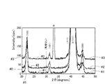
図4に、結晶化に対する成膜条件(Pb原料の流量)依存性を検討するためのXRDスペクトルを示す。図4中、スペクトル#1、#2及び#3はそれぞれ、表1中の試料番号に対応する。図4から明らかなように、異相は観察されず、全ての試料でPZT単相が得られていることが分かる。また、PZT薄膜の配向については、初期層のPb原料流量が多いほど基板の配向を反映した(111)方向へ結晶成長していることが分かる。
FIG. 4 shows an XRD spectrum for studying the dependency of the film formation condition (flow rate of Pb raw material) on crystallization. In FIG. 4,
なお、#2の試料について、アニール処理温度を実施例1と同様に変動させて得られた薄膜について、同様にしてXRDスペクトルを測定したところ、実施例1の場合と同様に、アニール処理温度を高くするにつれて結晶化が促進され、同様の結晶化傾向が得られた。
As for the
次に、図5に、上記で得られた各PZT薄膜を用いたPZTキャパシタに2Vの電圧を印加した時のリーク電流密度に対する成膜条件の依存性、すなわちリーク電流密度の初期層Pb原料流量依存性を示す。図5から明らかなように、リーク電流密度は、初期層のPb原料流量が低い試料ほど低いことが分かる。いずれの試料も、1.0E−4A/cm2以下であり、目的とするリーク電流密度を満足した。 Next, FIG. 5 shows the dependence of the film formation condition on the leakage current density when a voltage of 2 V is applied to the PZT capacitor using each PZT thin film obtained above, that is, the initial layer Pb raw material flow rate of the leakage current density. Indicates dependency. As can be seen from FIG. 5, the leakage current density is lower for samples with a lower Pb raw material flow rate in the initial layer. All the samples were 1.0E-4 A / cm 2 or less and satisfied the target leakage current density.
また、図6に、上記で得られた各PZT薄膜を用いたPZTキャパシタに0Vから4.0Vまでの電圧を印加した時の、各印加電圧における強誘電体キャパシタのQTV特性について、成膜条件依存性を示す。図6から明らかなように、Qswは初期層成膜時のPb原料流量に大きく依存し、初期層成膜時のPb原料流量が大きい試料ほどQswは大きく、また、低電圧でのQswの立ち上がりが良好になっていることが分かる。 FIG. 6 shows the film formation conditions for the QTV characteristics of the ferroelectric capacitor at each applied voltage when a voltage from 0 V to 4.0 V is applied to the PZT capacitor using each PZT thin film obtained above. Indicates dependency. As apparent from FIG. 6, Qsw greatly depends on the Pb raw material flow rate during the initial layer film formation, and the sample having a larger Pb raw material flow rate during the initial layer film formation has a higher Qsw, and the rise of Qsw at a low voltage. It turns out that is improving.
上記の結果から、適当な電気特性を有する単相PZT薄膜が得られる原料流量を求め、基板の配向を引きずったPZT薄膜であって、強誘電体キャパシタとして利用できる良好なQTV特性を有する薄膜を得るためには、初期層のPb原料流量をバルク層のPb原料流量と同量以上、好ましくはその流量以上にする必要があること、また、所定のアニール処理を実施する必要があることが分かる。 From the above results, a raw material flow rate for obtaining a single-phase PZT thin film having appropriate electrical characteristics was obtained, and a thin film having good QTV characteristics that can be used as a ferroelectric capacitor is a PZT thin film in which the orientation of the substrate is dragged. In order to obtain, it is understood that the Pb material flow rate of the initial layer needs to be equal to or higher than the Pb material flow rate of the bulk layer, preferably more than that flow rate, and that a predetermined annealing process needs to be performed. .
本実施例では、目的とするPZT薄膜を初期層とそれに続くバルク層とに分け、それぞれの層の成膜に際し、全成膜時間を一定にして初期層とバルク層との成膜時間(すなわち、膜厚)を変化させて成膜し、PZT薄膜の電気特性に対する成膜時間の依存性を検討した。この成膜条件を表2に示す。この場合、初期層とバルク層とでPb原料流量が多少異なっているが、成膜速度はほぼ一定とみなせるので、膜厚は成膜時間に比例するものとみなせる。 In this embodiment, the target PZT thin film is divided into an initial layer and a subsequent bulk layer, and when forming each layer, the total film formation time is kept constant, that is, the initial layer and the bulk layer are formed (that is, The film thickness was changed, and the dependence of the film formation time on the electrical characteristics of the PZT thin film was examined. Table 2 shows the film forming conditions. In this case, the Pb material flow rate is slightly different between the initial layer and the bulk layer, but since the film formation rate can be regarded as almost constant, the film thickness can be regarded as being proportional to the film formation time.
(表2)
上記成膜条件に従って、基板上にPZT薄膜の初期層及びバルク層を成膜した。いずれの試料の場合も、成膜後に500℃で結晶化アニール処理を施した。アニール処理後の薄膜上に上部電極を成膜し、次いで、500℃で回復アニール処理を施して、下地膜へのダメージを回復せしめた。かくして得られたPZT薄膜について、リーク電流密度及び分極反転電荷密度を実施例1と同様にして測定した。 In accordance with the film formation conditions, an initial layer and a bulk layer of a PZT thin film were formed on the substrate. In any case, crystallization annealing treatment was performed at 500 ° C. after film formation. An upper electrode was formed on the annealed thin film, and then a recovery annealing process was performed at 500 ° C. to recover damage to the underlying film. For the PZT thin film thus obtained, the leakage current density and the polarization inversion charge density were measured in the same manner as in Example 1.
図7に、上記で得られた各PZT薄膜を用いたPZTキャパシタに2Vの電圧を印加した時のリーク電流密度に対する初期層成膜時間(sec)の依存性を示す。図7から明らかなように、リーク電流密度は、初期層の成膜時間が短い領域では低く、特に変化はないが、初期層の成膜時間が50秒(膜厚は約10nm)を超えるとリーク電流密度は上昇し、100sec程度でほぼ1.0E−04A/cm2程度のリーク電流密度となっていることが分かる。 FIG. 7 shows the dependence of the initial layer deposition time (sec) on the leakage current density when a voltage of 2 V is applied to the PZT capacitor using each PZT thin film obtained above. As is clear from FIG. 7, the leakage current density is low in the region where the initial layer deposition time is short, and there is no particular change, but when the initial layer deposition time exceeds 50 seconds (the film thickness is about 10 nm). It can be seen that the leakage current density rises and is about 1.0E-04 A / cm 2 in about 100 seconds.
また、図8に、上記で得られた各PZT薄膜を用いたPZTキャパシタに0Vから4.0Vまでの電圧を印加した時の、各印加電圧における強誘電体キャパシタのQTV特性に対する成膜条件依存性を示す。図8中、#1、#2、#3及び#4はそれぞれ、表2中の試料番号に対応する。図8から明らかなように、Qswは、初期層の成膜時間を長くしていくと、その値は上昇し、低電圧での立ち上がりが良好になっていることが分かる。Qswは、2V印加で25μC/cm2以上であった。 Further, FIG. 8 shows the dependence on the film formation conditions for the QTV characteristics of the ferroelectric capacitor at each applied voltage when a voltage from 0 V to 4.0 V is applied to the PZT capacitor using each PZT thin film obtained above. Showing gender. In FIG. 8, # 1, # 2, # 3, and # 4 correspond to the sample numbers in Table 2, respectively. As can be seen from FIG. 8, Qsw increases as the initial layer deposition time is increased, and the rise at low voltage is good. Qsw was 25 μC / cm 2 or more when 2 V was applied.
上記の結果から、強誘電体キャパシタとして利用できるPZT薄膜を得るには、初期層の成膜時間を最適な範囲に調整することが望ましい。成膜時間を100sec以下(膜厚20nm以下)、好ましくは50sec以下(膜厚10nm以下)にすれば、Qswが2V印加で25μC/cm2以上、好ましくは30μC/cm2以上である薄膜を得ることができる。従って、初期層の膜厚としては、2nm〜20nm、好ましくは2nm〜10nmであれば、上記したような所望の電気特性を有する薄膜を得ることができるが、その範囲を外れるとリーク電流が高く、分極反転電荷密度が低い薄膜しか得られない。 From the above results, in order to obtain a PZT thin film that can be used as a ferroelectric capacitor, it is desirable to adjust the film formation time of the initial layer to an optimum range. The deposition time 100sec or less (thickness 20nm or less), preferably if below (thickness 10nm or less) 50 sec, Qsw is 25μC / cm 2 or more at 2V applied, preferably to obtain a thin film is 30 .mu.C / cm 2 or more be able to. Therefore, if the film thickness of the initial layer is 2 nm to 20 nm, preferably 2 nm to 10 nm, a thin film having the desired electrical characteristics as described above can be obtained. Only thin films with low polarization inversion charge density can be obtained.
なお、初期層の厚さを2番目の層の厚さよりも薄く、好ましくは10分の1以下、さらに好ましくは20分の1以下にすることにより、所望の電気特性を有する薄膜を得ることができるが、その範囲を外れるとリーク電流が高く、分極反転電荷密度が低い薄膜しか得られない。 Note that a thin film having desired electrical characteristics can be obtained by making the thickness of the initial layer thinner than the thickness of the second layer, preferably 1/10 or less, more preferably 1/20 or less. However, if it is out of the range, only a thin film having a high leakage current and a low polarization inversion charge density can be obtained.
本発明によれば、成膜初期の組成ずれを補正して膜厚方向に組成を制御することにより、また、成膜後に所定の条件でアニール処理を行うことにより、優れた電気特性を有する薄膜を製造することができるので、本発明は、半導体素子の高集積化、高性能化の進む半導体産業におけるCVD法による成膜プロセスに有効に適用できる。 According to the present invention, a thin film having excellent electrical characteristics can be obtained by correcting the composition deviation in the initial stage of film formation and controlling the composition in the film thickness direction, and by performing annealing treatment under predetermined conditions after film formation. Therefore, the present invention can be effectively applied to a film forming process by a CVD method in the semiconductor industry where semiconductor elements are highly integrated and have high performance.
1 真空排気システム 1a 圧力調整バルブ
2 反応室 2−1 基板ステージ
3 シャワープレート 4 成膜ガス配管
5 ガス混合器 6 原料ガス配管
7 気化システム 7a 原料供給部
8 配管 S 基板
DESCRIPTION OF
Claims (9)
前記Pb(thd) 2 を溶媒に溶かした液体、前記Zr(dmhd) 4 を溶媒に溶かした液体、前記Ti(i−PrO) 2 (thd) 2 を溶媒に溶かした液体を所定の流量で前記気化システムに供給することで、前記基板上に初期層を成膜した後、
前記Pb(thd) 2 を溶媒に溶かした液体の流量を前記初期層の成膜時の流量よりも少なくして、前記初期層の上にバルク層を成膜することを特徴とする薄膜製造方法。 Pb a (thd) 2, Zr (dmhd ) 4 and Ti (i-PrO) 2 ( thd) deposition gas containing a raw material gas vaporized by using a liquid vaporization system dissolved 2 in a solvent and the reaction gas In a thin film manufacturing method for forming a PZT thin film on a substrate that is introduced into a reaction chamber through a gas introduction means and heated to a temperature equal to or higher than a decomposition temperature of a source gas,
The liquid in which the Pb (thd) 2 is dissolved in the solvent, the liquid in which the Zr (dmhd) 4 is dissolved in the solvent, and the liquid in which the Ti (i-PrO) 2 (thd) 2 is dissolved in the solvent are added at a predetermined flow rate. By supplying the vaporization system, after depositing the initial layer on the substrate ,
A method for producing a thin film , comprising forming a bulk layer on the initial layer by reducing a flow rate of the liquid obtained by dissolving Pb (thd) 2 in a solvent to a flow rate at the time of forming the initial layer. .
前記上部電極の成膜時のダメージを回復させる回復アニール処理を、前記結晶化アニール処理と同じ条件で行うことを特徴とする請求項3記載の薄膜製造方法。 After the sintering crystallization annealing, forming a top electrode on the bulk layer,
The recovery annealing process for recovering the damage at the deposition of the upper electrode, the thin film manufacturing method of claim 3 wherein the row Ukoto characterized under the same conditions as the crystallization annealing process.
Priority Applications (1)
| Application Number | Priority Date | Filing Date | Title |
|---|---|---|---|
| JP2003403975A JP4205565B2 (en) | 2003-12-03 | 2003-12-03 | Thin film manufacturing method |
Applications Claiming Priority (1)
| Application Number | Priority Date | Filing Date | Title |
|---|---|---|---|
| JP2003403975A JP4205565B2 (en) | 2003-12-03 | 2003-12-03 | Thin film manufacturing method |
Publications (3)
| Publication Number | Publication Date |
|---|---|
| JP2005166965A JP2005166965A (en) | 2005-06-23 |
| JP2005166965A5 JP2005166965A5 (en) | 2006-12-07 |
| JP4205565B2 true JP4205565B2 (en) | 2009-01-07 |
Family
ID=34727077
Family Applications (1)
| Application Number | Title | Priority Date | Filing Date |
|---|---|---|---|
| JP2003403975A Expired - Lifetime JP4205565B2 (en) | 2003-12-03 | 2003-12-03 | Thin film manufacturing method |
Country Status (1)
| Country | Link |
|---|---|
| JP (1) | JP4205565B2 (en) |
Families Citing this family (4)
| Publication number | Priority date | Publication date | Assignee | Title |
|---|---|---|---|---|
| US20070218200A1 (en) * | 2006-03-16 | 2007-09-20 | Kenji Suzuki | Method and apparatus for reducing particle formation in a vapor distribution system |
| JP5248025B2 (en) * | 2007-03-01 | 2013-07-31 | 東京エレクトロン株式会社 | Method for forming SrTiO3 film and computer-readable storage medium |
| WO2011070945A1 (en) * | 2009-12-11 | 2011-06-16 | 株式会社アルバック | Thin film manufacturing apparatus, thin film manufacturing method, and method for manufacturing semiconductor device |
| KR102433290B1 (en) * | 2018-02-08 | 2022-08-17 | 에스케이하이닉스 주식회사 | Method of Fabricating Ferroelectric Device |
-
2003
- 2003-12-03 JP JP2003403975A patent/JP4205565B2/en not_active Expired - Lifetime
Also Published As
| Publication number | Publication date |
|---|---|
| JP2005166965A (en) | 2005-06-23 |
Similar Documents
| Publication | Publication Date | Title |
|---|---|---|
| JP3462852B2 (en) | Method and apparatus for producing thin films by chemical vapor deposition | |
| US5572052A (en) | Electronic device using zirconate titanate and barium titanate ferroelectrics in insulating layer | |
| US6056994A (en) | Liquid deposition methods of fabricating layered superlattice materials | |
| EP2620975A1 (en) | Thin film production process and thin film production device | |
| JPH0927602A (en) | Manufacture of capacitor and large capacitance capacitor | |
| JP3109485B2 (en) | Vapor phase growth method of metal oxide dielectric film | |
| JPH0927601A (en) | Manufacture of memory and ferroelectric memory | |
| KR100945096B1 (en) | Method for manufacturing capacitor | |
| US7629183B2 (en) | Method for manufacturing semiconductor device and computer storage medium | |
| WO2000036640A1 (en) | Method of forming thin film | |
| TW437058B (en) | Vapor growth method and device for metal oxide dielectric film | |
| JP4205565B2 (en) | Thin film manufacturing method | |
| JP4628954B2 (en) | Oxide thin film manufacturing method | |
| JP2001127258A (en) | Semiconductor device and manufacturing method therefor | |
| JPH0689986A (en) | Electronic device and its manufacturing method | |
| US20050167713A1 (en) | Ferroelectric capacitor and method of production of same | |
| JP3171246B2 (en) | Vapor phase growth method of metal oxide dielectric film | |
| JP3353835B2 (en) | Vapor phase growth method of metal oxide dielectric film | |
| EP1120475A1 (en) | A method and system for MOCVD of PGO films | |
| JP4473540B2 (en) | Thin film manufacturing method and particle number evaluation method | |
| JP2004289035A (en) | Chemical vapor deposition method and chemical vapor deposition apparatus | |
| Cho et al. | Low temperature MOCVD of BST thin film for high density DRAMs | |
| Cho et al. | LOWERING OF LEAKAGE CURRENT DENSITY OF (Ba, Sr) TiO3 THIN FILMS BY TWO-STEP DEPOSITION METHOD | |
| JP2014150191A (en) | Pzt film manufacturing method and deposition apparatus |
Legal Events
| Date | Code | Title | Description |
|---|---|---|---|
| A521 | Request for written amendment filed |
Free format text: JAPANESE INTERMEDIATE CODE: A523 Effective date: 20061020 |
|
| A621 | Written request for application examination |
Free format text: JAPANESE INTERMEDIATE CODE: A621 Effective date: 20061020 |
|
| A977 | Report on retrieval |
Free format text: JAPANESE INTERMEDIATE CODE: A971007 Effective date: 20070402 |
|
| A131 | Notification of reasons for refusal |
Free format text: JAPANESE INTERMEDIATE CODE: A131 Effective date: 20080527 |
|
| A521 | Request for written amendment filed |
Free format text: JAPANESE INTERMEDIATE CODE: A523 Effective date: 20080728 |
|
| TRDD | Decision of grant or rejection written | ||
| A01 | Written decision to grant a patent or to grant a registration (utility model) |
Free format text: JAPANESE INTERMEDIATE CODE: A01 Effective date: 20080930 |
|
| A01 | Written decision to grant a patent or to grant a registration (utility model) |
Free format text: JAPANESE INTERMEDIATE CODE: A01 |
|
| A61 | First payment of annual fees (during grant procedure) |
Free format text: JAPANESE INTERMEDIATE CODE: A61 Effective date: 20081016 |
|
| FPAY | Renewal fee payment (event date is renewal date of database) |
Free format text: PAYMENT UNTIL: 20111024 Year of fee payment: 3 |
|
| R150 | Certificate of patent or registration of utility model |
Free format text: JAPANESE INTERMEDIATE CODE: R150 Ref document number: 4205565 Country of ref document: JP Free format text: JAPANESE INTERMEDIATE CODE: R150 |
|
| FPAY | Renewal fee payment (event date is renewal date of database) |
Free format text: PAYMENT UNTIL: 20111024 Year of fee payment: 3 |
|
| FPAY | Renewal fee payment (event date is renewal date of database) |
Free format text: PAYMENT UNTIL: 20141024 Year of fee payment: 6 |
|
| R250 | Receipt of annual fees |
Free format text: JAPANESE INTERMEDIATE CODE: R250 |
|
| R250 | Receipt of annual fees |
Free format text: JAPANESE INTERMEDIATE CODE: R250 |
|
| R250 | Receipt of annual fees |
Free format text: JAPANESE INTERMEDIATE CODE: R250 |
|
| R250 | Receipt of annual fees |
Free format text: JAPANESE INTERMEDIATE CODE: R250 |
|
| R250 | Receipt of annual fees |
Free format text: JAPANESE INTERMEDIATE CODE: R250 |
|
| R250 | Receipt of annual fees |
Free format text: JAPANESE INTERMEDIATE CODE: R250 |
|
| R250 | Receipt of annual fees |
Free format text: JAPANESE INTERMEDIATE CODE: R250 |
|
| R250 | Receipt of annual fees |
Free format text: JAPANESE INTERMEDIATE CODE: R250 |
|
| R250 | Receipt of annual fees |
Free format text: JAPANESE INTERMEDIATE CODE: R250 |