EP1120475A1 - A method and system for MOCVD of PGO films - Google Patents
A method and system for MOCVD of PGO films Download PDFInfo
- Publication number
- EP1120475A1 EP1120475A1 EP01300635A EP01300635A EP1120475A1 EP 1120475 A1 EP1120475 A1 EP 1120475A1 EP 01300635 A EP01300635 A EP 01300635A EP 01300635 A EP01300635 A EP 01300635A EP 1120475 A1 EP1120475 A1 EP 1120475A1
- Authority
- EP
- European Patent Office
- Prior art keywords
- substrate
- depositing
- annealing
- temperature
- precursor
- Prior art date
- Legal status (The legal status is an assumption and is not a legal conclusion. Google has not performed a legal analysis and makes no representation as to the accuracy of the status listed.)
- Withdrawn
Links
Images


Classifications
-
- H—ELECTRICITY
- H01—ELECTRIC ELEMENTS
- H01L—SEMICONDUCTOR DEVICES NOT COVERED BY CLASS H10
- H01L21/00—Processes or apparatus adapted for the manufacture or treatment of semiconductor or solid state devices or of parts thereof
- H01L21/02—Manufacture or treatment of semiconductor devices or of parts thereof
- H01L21/04—Manufacture or treatment of semiconductor devices or of parts thereof the devices having at least one potential-jump barrier or surface barrier, e.g. PN junction, depletion layer or carrier concentration layer
- H01L21/18—Manufacture or treatment of semiconductor devices or of parts thereof the devices having at least one potential-jump barrier or surface barrier, e.g. PN junction, depletion layer or carrier concentration layer the devices having semiconductor bodies comprising elements of Group IV of the Periodic System or AIIIBV compounds with or without impurities, e.g. doping materials
- H01L21/30—Treatment of semiconductor bodies using processes or apparatus not provided for in groups H01L21/20 - H01L21/26
- H01L21/324—Thermal treatment for modifying the properties of semiconductor bodies, e.g. annealing, sintering
-
- C—CHEMISTRY; METALLURGY
- C23—COATING METALLIC MATERIAL; COATING MATERIAL WITH METALLIC MATERIAL; CHEMICAL SURFACE TREATMENT; DIFFUSION TREATMENT OF METALLIC MATERIAL; COATING BY VACUUM EVAPORATION, BY SPUTTERING, BY ION IMPLANTATION OR BY CHEMICAL VAPOUR DEPOSITION, IN GENERAL; INHIBITING CORROSION OF METALLIC MATERIAL OR INCRUSTATION IN GENERAL
- C23C—COATING METALLIC MATERIAL; COATING MATERIAL WITH METALLIC MATERIAL; SURFACE TREATMENT OF METALLIC MATERIAL BY DIFFUSION INTO THE SURFACE, BY CHEMICAL CONVERSION OR SUBSTITUTION; COATING BY VACUUM EVAPORATION, BY SPUTTERING, BY ION IMPLANTATION OR BY CHEMICAL VAPOUR DEPOSITION, IN GENERAL
- C23C16/00—Chemical coating by decomposition of gaseous compounds, without leaving reaction products of surface material in the coating, i.e. chemical vapour deposition [CVD] processes
- C23C16/44—Chemical coating by decomposition of gaseous compounds, without leaving reaction products of surface material in the coating, i.e. chemical vapour deposition [CVD] processes characterised by the method of coating
- C23C16/455—Chemical coating by decomposition of gaseous compounds, without leaving reaction products of surface material in the coating, i.e. chemical vapour deposition [CVD] processes characterised by the method of coating characterised by the method used for introducing gases into reaction chamber or for modifying gas flows in reaction chamber
- C23C16/45514—Mixing in close vicinity to the substrate
-
- C—CHEMISTRY; METALLURGY
- C23—COATING METALLIC MATERIAL; COATING MATERIAL WITH METALLIC MATERIAL; CHEMICAL SURFACE TREATMENT; DIFFUSION TREATMENT OF METALLIC MATERIAL; COATING BY VACUUM EVAPORATION, BY SPUTTERING, BY ION IMPLANTATION OR BY CHEMICAL VAPOUR DEPOSITION, IN GENERAL; INHIBITING CORROSION OF METALLIC MATERIAL OR INCRUSTATION IN GENERAL
- C23C—COATING METALLIC MATERIAL; COATING MATERIAL WITH METALLIC MATERIAL; SURFACE TREATMENT OF METALLIC MATERIAL BY DIFFUSION INTO THE SURFACE, BY CHEMICAL CONVERSION OR SUBSTITUTION; COATING BY VACUUM EVAPORATION, BY SPUTTERING, BY ION IMPLANTATION OR BY CHEMICAL VAPOUR DEPOSITION, IN GENERAL
- C23C16/00—Chemical coating by decomposition of gaseous compounds, without leaving reaction products of surface material in the coating, i.e. chemical vapour deposition [CVD] processes
- C23C16/22—Chemical coating by decomposition of gaseous compounds, without leaving reaction products of surface material in the coating, i.e. chemical vapour deposition [CVD] processes characterised by the deposition of inorganic material, other than metallic material
- C23C16/30—Deposition of compounds, mixtures or solid solutions, e.g. borides, carbides, nitrides
- C23C16/40—Oxides
-
- C—CHEMISTRY; METALLURGY
- C30—CRYSTAL GROWTH
- C30B—SINGLE-CRYSTAL GROWTH; UNIDIRECTIONAL SOLIDIFICATION OF EUTECTIC MATERIAL OR UNIDIRECTIONAL DEMIXING OF EUTECTOID MATERIAL; REFINING BY ZONE-MELTING OF MATERIAL; PRODUCTION OF A HOMOGENEOUS POLYCRYSTALLINE MATERIAL WITH DEFINED STRUCTURE; SINGLE CRYSTALS OR HOMOGENEOUS POLYCRYSTALLINE MATERIAL WITH DEFINED STRUCTURE; AFTER-TREATMENT OF SINGLE CRYSTALS OR A HOMOGENEOUS POLYCRYSTALLINE MATERIAL WITH DEFINED STRUCTURE; APPARATUS THEREFOR
- C30B25/00—Single-crystal growth by chemical reaction of reactive gases, e.g. chemical vapour-deposition growth
- C30B25/02—Epitaxial-layer growth
-
- C—CHEMISTRY; METALLURGY
- C30—CRYSTAL GROWTH
- C30B—SINGLE-CRYSTAL GROWTH; UNIDIRECTIONAL SOLIDIFICATION OF EUTECTIC MATERIAL OR UNIDIRECTIONAL DEMIXING OF EUTECTOID MATERIAL; REFINING BY ZONE-MELTING OF MATERIAL; PRODUCTION OF A HOMOGENEOUS POLYCRYSTALLINE MATERIAL WITH DEFINED STRUCTURE; SINGLE CRYSTALS OR HOMOGENEOUS POLYCRYSTALLINE MATERIAL WITH DEFINED STRUCTURE; AFTER-TREATMENT OF SINGLE CRYSTALS OR A HOMOGENEOUS POLYCRYSTALLINE MATERIAL WITH DEFINED STRUCTURE; APPARATUS THEREFOR
- C30B29/00—Single crystals or homogeneous polycrystalline material with defined structure characterised by the material or by their shape
- C30B29/10—Inorganic compounds or compositions
- C30B29/16—Oxides
- C30B29/22—Complex oxides
- C30B29/32—Titanates; Germanates; Molybdates; Tungstates
Definitions
- the present invention relates to metalorganic chemical vapor deposition (MOCVD) and annealing processes for depositing lead germanium oxide (PGO) thin film materials, and oxide thin films, particularly Pb- and Bi-based oxide thin films, the precursors of which react with oxygen when in a gas phase.
- MOCVD metalorganic chemical vapor deposition
- PGO lead germanium oxide
- oxide thin films particularly Pb- and Bi-based oxide thin films
- Ferroelectric films have attracted great interest in recent years because of their applications in electro-optic, pyroelectric, frequency agile electronic and non-volatile memory devices.
- the fabrication and characterization of ferroelectric lead germanium oxide thin films (PGO), such as Pb 5 Ge 3 O 11 and Pb 3 GeO 5 are of current interest.
- Lead germanite (Pb 5 Ge 3 O 11 ) is a relative new member of ferroelectric family.
- the ferroelectricity in this material was first discovered by Iwasaki et al ., Applied Physics Letters, 18, 444 (1971), 43, 4907 (1972). Other work with this material is described in Ferroelectric memory cell for VLSI ram array and method of making the same, U.S. Patent Application Serial No.
- CVD Chemical vapor deposition
- the electronics industry has extensive experience and tested equipment for CVD technology. This legacy experience and equipment is readily applied to a new CVD processes.
- the control of key variables such as stoichiometry and film thickness, and the coating of a wide variety of substrate geometries are possible with CVD.
- Forming thin films by CVD permits the integration of these materials into existing device production technologies.
- CVD also permits the formation of layers of refractory materials that are epitaxially related to substrates having close crystal structures.
- Fig. 2 is a somewhat schematic representation of the system of the invention.
- Fig. 4 depicts the fatigue property of the capacitor of Fig. 3.
- Fig. 9 depicts the fatigue property of the capacitor of Fig. 8.
- Fig. 11 depicts the retention properties of the capacitor of Fig. 8.
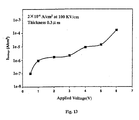
- Fig. 13 depicts the leakage current vs. applied voltage of the capacitor of Fig. 8.
- the system of the invention utilizes separated injection lines and gas curtain flows, or extending lines, to avoid a pre-reaction between a Pb precursor, a Ge precursor and oxygen, all in gas phases, before deposition on the surface of a subject substrate.
- This system uses between about 2% and about 50% excess Pb, along with a high oxygen flow, having a partial pressure of about 10% to about 60%, which is introduced into a reactor, to compensate for Pb loss in the processes and avoid any Pb and/or O deficiency.
- An appropriate second phase of Pb 3 GeO 5 can decrease the deposition temperature and improve the ferroelectric properties of Pb 5 Ge 3 O 11 thin films.
- Fig. 1 is a flow chart showing the processing steps for making a metal-PGO-metal capacitor, generally at 20.
- Polycrystalline Pb 5 Ge 3 O 11 thin films, with preferred C-axis orientation, and Pb 5 Ge 3 O 11 with Pb 3 GeO 5 thin films, with very good ferroelectric properties were deposited on 6" Ir (150nm)-Ti(25nm)-SiO 2 (100nm)-Si using the MOCVD processes.
- a three step process is used to make high quality PGO thin films.
- First step 22 is a two sub-step process, and includes depositing a nucleation, or buffer, layer, and then further depositing material to promote grain growth.
- Pb(thd) 2 and Ge(ETO) 4 having a molar ratio of 5:3 with Pb having an excess of from about 1% to about 30% over the stoichiometric requirement are dissolved in a mixed solvent of tetrahydrofuran, isopropanol and tetraglyme, in the molar ratio of 8:2:1.
- the precursor solutions have a concentration of 0.1 - 0.3 M/L of PGO.
- the solution is injected into a vaporizer at between about 180°C to about 250°C, by a pump at a rate of 0.1 - 0.5 ml/min to form the precursor gases.
- the precursor gases are introduced into reaction chamber 42 using a preheated argon flow at about 180° C to about 250°C.
- the deposition temperatures and pressure are about 400°C to about 650°C and 2 - 20 torr, respectively.
- the shroud flow is introduced into reaction chamber 42 with an Ar flow of about 2000 sccm to about 6000 sccm, with an oxygen flow of about 500 sccm to about 3000 sccm.
- the basic composition, phase, and ferroelectric and electrical properties of the polycrystalline Pb 5 Ge 3 O 11 thin films with preferred C-axis orientation and polycrystalline Pb 5 Ce 3 O 11 thin films with second phase Pb 3 GeO 5 were measured.
- the compositions of the PGO thin films were analyzed by using energy dispersion X-ray analysis (EDX).
- the phases of the films were identified using x-ray diffraction.
- the thickness and surface morphologies of the films on Ir/Ti/SiO 2 /Si substrates were investigated by scanning electronic microscope.
- the leakage currents and dielectric constants of the films were measured using HP 4155-6 precision semiconductor parameter analyzer and Keithley 182 CV analyzer respectively.
- the ferroelectric properties of the films were measured by a standardized RT66A tester. Analysis results for the two kinds of PGO thin films made by the MOCVD and annealing processes are now presented.
- the fatigue properties of the Pb 5 Ge 3 O 11 thin film shown in Fig. 4 at 64, 66 were measured at switch cycles 1x10 9 .
- the Pb 5 Ge 3 O 11 thin films on Ir substrate are nearly fatigue free, as shown by hysteresis loop 64 of the Pb 5 Ge 3 O 11 films before fatigue, and the hysteresis loop 66 after fatigue.
- the experimental results demonstrated that the composition of the PGO thin film with good ferroelectric properties is Pb 5 Ge 3 O 11 having an appropriate excess Pb layer, which is located between Pb 5 Ge 3 O 11 and Pb 3 GeO 5 in PbO - GeO 2 phase diagram.
- a single phase Pb 5 Ge 3 O 11 with C-axis orientation has the best ferroelectric properties.
- excess Pb, or the second phase of Pb 3 GeO 5 is necessary to make up for the Pb loss and avoid a Pb and/or O deficiency.
- the Pb excess improves the ferroelectric properties of MOCVD PGO thin films.
- Fig. 8 depicts the hysteresis loop of the PGO thin films on Ir substrate before annealing at 70, and after TE at 72.
- the hysteresis loop with 2Pr: 4.15 ⁇ C/cm 2 and 217 KV/cm was square, symmetric and saturated.
- the fatigue properties of the PGO thin film were measured at switch cycles 1x10 6 , 1x10 9 and 1x10 10 .
- the retention properties of the PGO thin films are depicted in Fig. 11.
- the retained charge of the PGO thin films dropped nearly 50% at most when the waiting time increased to 10 seconds, after that, the retained charge was stable with increasing waiting time.
- the retention properties of PGO thin films were similar with that of Pb(Zr, Ti)O 3 (PZT) thin films.
- the imprint properties of the PGO thin film were also measured and are depicted in Fig. 12) It was found that the remanent polarization of the PGO film decreased from 1.88 ⁇ C/cm 2 to 1.41 ⁇ C/cm 2 , and from 1.91 ⁇ C/cm 2 to 1.40 ⁇ C/cm 2 at writing voltage 6V and -6V, respectively, after an imprint at 100°C for 100 minutes. The results showed very small imprint properties of the PGO thin films.
Abstract
Description
- The present invention relates to metalorganic chemical vapor deposition (MOCVD) and annealing processes for depositing lead germanium oxide (PGO) thin film materials, and oxide thin films, particularly Pb- and Bi-based oxide thin films, the precursors of which react with oxygen when in a gas phase.
- Ferroelectric films have attracted great interest in recent years because of their applications in electro-optic, pyroelectric, frequency agile electronic and non-volatile memory devices. The fabrication and characterization of ferroelectric lead germanium oxide thin films (PGO), such as Pb5Ge3O11 and Pb3GeO5, are of current interest. Lead germanite (Pb5Ge3O11) is a relative new member of ferroelectric family. The ferroelectricity in this material was first discovered by Iwasaki et al., Applied Physics Letters, 18, 444 (1971), 43, 4907 (1972). Other work with this material is described in Ferroelectric memory cell for VLSI ram array and method of making the same, U.S. Patent Application Serial No. 08/870,375, of Hsu et al., filed June 6, 1997. The piezoelectric, dielectric and electric-optic properties of single crystal and polycrystalline materials have been reported in the literature. Pb5Ge3O11 is an optically active and ferroelectric material, has a moderate dielectric constant and a small remanent polarization, which make it particularly suitable for ferroelectric non-volatile memory devices such as metal ferroelectric metal oxide silicon (MFMOS), metal ferroelectric metal silicon (MFMS), metal ferroelectric insulators silicon (MFIS), metal-insulator-ferroelectric-silicon (MIFS), metal-insulator ferroelectric insulators silicon (MIFIS), and metal-ferroelectric-silicon (MFS) type memories, Krupanidhi et al., Proceedings of the 3d International Symposium on Integrated Ferroelectrics, 100 (1991). Pb5Ge3O11 also has potential in thermal detector applications because of its pyroelectric and dielectric characteristics. Pb3GeO5 is a ferroelastic material, which may be used for microelectromechanical systems (MEMS) applications.
- Thin films of lead germanite have been made by thermal evaporation and flash evaporation, A. Mansingh et al., J. Appl. Phys. 51, 5408 (1980); DC reactive sputtering, H. Schmitt et al., Ferroelectrics, 56, 141(1984), laser ablation, S.B. Krupanidhi et al., Proceedings of the 3d International Symposium on Integrated Ferroelectrics, 100 (1991); and C.J. Peng et al., Appl. Phys. Lett. 60, 827 (1992), Sol-gel technique J.J. Lee et al., Appl. Phys. Lett. 60, 827 (1992), and CVD, as described in Chemical vapor deposition of Pb5Ge3O11 thin film for ferroelectric applications, Chien-Hsiung Peng and J.J. Lee, Serial No. 09/291,688, filed April 13, 1999. Y. Nakao et al. Study on Ferroelectric Thin films for Application to NDRO Nonvolatile Memories Integrated Ferroelectrics, Vol. 6, 23 (1995). U.S. Patent No. 5,204,314, to Kirlin et al., for Method for delivering an involatile reagent in vapor form to a CVD reactor, granted April 20, 1993.
- Chemical vapor deposition (CVD) is a particularly attractive method for semiconductor industries because it is readily scaled up to production runs and provides very good step coverage. The electronics industry has extensive experience and tested equipment for CVD technology. This legacy experience and equipment is readily applied to a new CVD processes. In general, the control of key variables such as stoichiometry and film thickness, and the coating of a wide variety of substrate geometries are possible with CVD. Forming thin films by CVD permits the integration of these materials into existing device production technologies. CVD also permits the formation of layers of refractory materials that are epitaxially related to substrates having close crystal structures.
- CVD requires that the element source reagents must be sufficiently volatile to permit gas phase transport into the deposition reactor. The element source reagent must decompose in the reactor to deposit only the desired element at the desired growth temperature. Premature gas phase reaction, leading to particulate formation, must not occur, nor should the source reagent decompose in the reactant lines before reaching the reactor deposition chamber. Obtaining optimal conditions to deposit a specific compound requires precise control of stoichiometry that can be achieved only if the reagent is delivered into the reactor in a desired condition.
- For PGO (Pb5Ge3O11 and Pb3GeO5) films, the content of lead to germanium is very high, i.e., 5:3 and 3:1, respectively. Because of Pb loss in the thermal MOCVD process, an excess Pb concentration and a high oxygen partial pressure must be used to make stoichiometric PGO thin films and avoid the Pb and O deficiency.
- The Pb precursors for MOCVD PGO film are liquids or solids that can be sublimed into a gas phase and transported into a reactor. The process window of Pb precursors is very narrow, i.e., the sublimation temperature of the Pb precursors is close to the decomposition and condensation temperature, in which case the reagent may begin to decompose or condense in the reactant lines before reaching the reactor, making it very difficult to control the stoichiometry of the deposited films. The Pb precursor gas easily reacts with oxygen in the gas phase before deposition, which results in large particles and a cloudy film, especially at higher deposition temperatures.
- In a traditional MOCVD process for forming oxide thin films, oxygen is mixed with thin film precursors. The mixed gases are injected into a reactor, or oxygen and the precursors are individually directed into a shower head and mixed in the shower head before deposition. these techniques allow premature gas phase reaction to occur in the reactant lines and in the shower head, which causes particulate formation, especially at high growth rates and at high deposition temperature. To insure precise deposition of oxide thin films, a high O2 partial pressure and distribution are required. A low O2 partial pressure results in incomplete decomposition of the precursors and incomplete oxidation of thin films, as well as contamination of carbon in the films, which causes the films to have a high leakage current. A high O2 partial pressure allows the reaction between the precursor and oxygen to occur in the gas phase. In the case of large area substrates, a non-homogeneous distribution of oxygen causes non-uniform thin films. Therefore, traditional MOCVD processes cannot produce high quality, large area PGO thin films with a high growth rates at high deposition temperature. For these reasons, ferroelectric PGO thin films have not been made by MOCVD.
- A method of making ferroelectric PGO thin films includes depositing Pb and Ge on a substrate using a thermal MOCVD process, wherein the Pb and Ge precursor gases are separately supplied to a region adjacent the substrate; annealing the substrate in a first annealing step; forming top electrodes on the substrate; and annealing the substrate in a second annealing step. A system for forming ferroelectric PGO thin films includes a reaction chamber, having a substrate support therein; a substrate located on said substrate support; precursor gas lines extending from a precursor gas source into said reaction chamber; background gas lines for providing a background gas into said reaction chamber; and separation means for separating the precursor gases until the precursor gases are adjacent said substrate.
- An object of the invention is to provide a metalorganic chemical vapor deposition and annealing processes for lead germanium oxide (PGO) thin film materials.
- Another object of the invention is to provide a system for performing metalorganic chemical vapor deposition and annealing processes for lead germanium oxide (PGO) thin film materials
- These and other objects and advantages of the invention will become more fully apparent as the description which follows is read in conjunction with the drawings.
- Fig. 1 is a flow chart depicting the steps of the invention.
- Fig. 2 is a somewhat schematic representation of the system of the invention.
- Fig. 3 depicts a hysteresis loop of a Pt - Pb5Ge3O11 - Ir capacitor having a C-axis orientation, constructed according to the invention..
- Fig. 4 depicts the fatigue property of the capacitor of Fig. 3.
- Fig. 5 depicts the hysteresis loops of the capacitor of Fig. 3.
- Fig. 6 depicts the leakage current vs. applied voltage of the capacitor of Fig. 3.
- Fig. 7 depicts the dielectric constant vs applied voltage the capacitor of Fig. 3.
- Fig. 8 depicts a hysteresis loop of a Pt - Pb5Ge3O11 with Pb3GeO5 - Ir capacitor constructed according to the invention.
- Fig. 9 depicts the fatigue property of the capacitor of Fig. 8.
- Fig. 10 depicts the hysteresis loops of the capacitor of Fig. 8, before and after fatigue of 1x10⁻⁹ switch cycles.
- Fig. 11 depicts the retention properties of the capacitor of Fig. 8.
- Fig. 12 depicts the imprint properties of the capacitor of Fig. 8.
- Fig. 13 depicts the leakage current vs. applied voltage of the capacitor of Fig. 8.
- Fig. 14 depicts the dielectric constant vs. applied voltage of the capacitor of Fig. 8.
- The system of the invention utilizes separated injection lines and gas curtain flows, or extending lines, to avoid a pre-reaction between a Pb precursor, a Ge precursor and oxygen, all in gas phases, before deposition on the surface of a subject substrate. This system uses between about 2% and about 50% excess Pb, along with a high oxygen flow, having a partial pressure of about 10% to about 60%, which is introduced into a reactor, to compensate for Pb loss in the processes and avoid any Pb and/or O deficiency. An appropriate second phase of Pb3GeO5 can decrease the deposition temperature and improve the ferroelectric properties of Pb5Ge3O11 thin films.
- Fig. 1 is a flow chart showing the processing steps for making a metal-PGO-metal capacitor, generally at 20. Polycrystalline Pb5Ge3O11 thin films, with preferred C-axis orientation, and Pb5Ge3O11 with Pb3GeO5 thin films, with very good ferroelectric properties were deposited on 6" Ir (150nm)-Ti(25nm)-SiO2(100nm)-Si using the MOCVD processes. A three step process is used to make high quality PGO thin films. First step 22 is a two sub-step process, and includes depositing a nucleation, or buffer, layer, and then further depositing material to promote grain growth. A thermal MOCVD deposition process, which takes place at a relatively low deposition temperature, below 700°C, is used to deposit high quality PGO films with excellent step coverage. In first step 22, Pb and Ge precursors 24 and O2, 26, are provided in gas phase compounds, along with a suitable substrate, such as Ir or Pt on a layer of Ti, which is carried on a layer of SiO2, which is on a Si substrate. The thermal MOCVD processes may be used to improve lattice mismatch between the film and substrates and to produce homogeneous and preferred orientation PGO thin films. The distribution of oxygen and reactant flow is controlled across the large deposition area covering one or multiple wafers.
- The second step is a RTP (Rapid Thermal Process) or
thermal annealing step 30, a first annealing step, which takes place in a O2, or Pb and O2,atmosphere 32 to achieve desired grain size and properties beforetop electrode deposition 34 takes place. The third step is another RTP orthermal annealing step 36, a second annealing step, which also takes place in an O2, or Pb and O2,atmosphere 38 to improve interface properties between the film and top electrodes. This novel process offers high quality PGO thin films over large area substrates with high growth rates - Referring now to Fig. 2, a system constructed according to the invention is depicted generally at 40.
System 40 utilizes separated inject lines and gas curtain flows, or extended reactant lines, to avoid early reaction between the Pb and Ge precursors and oxygen before deposition on the surface of the substrate.System 40 includes areaction chamber 42, which is fed byoxygen lines 44, control, or background,gas lines 46, andreactant lines 48. The background gas lines 4b feed agas curtain flow 50, in the preferred embodiment. Asubstrate 52 is supported on a suitable mount. Gas outflow 54 is provided. - The Pb and Ge precursor gases are injected into the reactor from
lines 48, and three mass flow controllers (MFC) are used to control the distribution of the precursor gases. The oxygen is injected into the reactor fromline 44, and three MFCs, or needle valves, are used to control the distribution of the oxygen. As the process takes place in an oxygen atmosphere, oxygen is the background gas, and may be provided as pure O2, N2O, or a mixture of O2 and N2O. In the preferred embodiment, an Ar curtain flow is used to separate the oxygen and precursor gases. Alternately, lines 44, 48 may be extended to introduce oxygen close to the surface of the substrate. The gas curtain flow and the extended precursor gas lines are referred to herein as precursor gas separation means.Lines reaction chamber 42 and outflow 54 are provided with a heating system, which, in the preferred embodiment, takes the form of a controlled heating system, for maintaining the precursor gases, curtain gases and background gases at a temperature to insure that the gases remain in an appropriate gas phase. The lines and reaction chamber wall may be wrapped in a heat tape, or enveloped in a silicon oil heating mechanism to maintain an appropriate temperature. The heating system includes, in the preferred embodiment, thermocouple heat sensors to provide input for the control mechanism. - The precursors for PGO thin films are listed in Table 1.
Properties of precursors for PGO thin films Precursors Formula Vapor Pressure (mm Hg) Decomposition Temperature(°C) Pb(TMHD)2 Pb(C11H19O2)2 180°C/0.05 325°C Ge(ETO)4 Ge(C2H5O)4 b.p. 185.5°C - Pb(thd)2 and Ge(ETO)4, having a molar ratio of 5:3 with Pb having an excess of from about 1% to about 30% over the stoichiometric requirement are dissolved in a mixed solvent of tetrahydrofuran, isopropanol and tetraglyme, in the molar ratio of 8:2:1. The precursor solutions have a concentration of 0.1 - 0.3 M/L of PGO. The solution is injected into a vaporizer at between about 180°C to about 250°C, by a pump at a rate of 0.1 - 0.5 ml/min to form the precursor gases. The precursor gases are introduced into
reaction chamber 42 using a preheated argon flow at about 180° C to about 250°C. The deposition temperatures and pressure are about 400°C to about 650°C and 2 - 20 torr, respectively. The shroud flow is introduced intoreaction chamber 42 with an Ar flow of about 2000 sccm to about 6000 sccm, with an oxygen flow of about 500 sccm to about 3000 sccm. - For MOCVD first step 22, a two sub-step MOCVD process may be used to improve lattice mismatch between the film and the substrates and get homogeneous and preferred orientation PGO thin films. In the first sub-step MOCVD process a very thin nucleation layer of the desired materials, or a buffer layer, is deposited at a relatively low temperature of about 400°C to about 500°C. In the second sub-step, the deposition temperatures increased to about 500°C to about 700°C, to promote grain growth. After deposition, the PGO films are cooled to room temperature in am oxygen atmosphere.
- In
second step 30, the PGO thin films are transferred to RTP, or thermal oven, for annealing in O2, or Pb and O2, atmosphere, with an appropriate Pb and O2 partial pressure and temperature of about 500°C to about 750°C, to achieve desired grain size and properties. - In
third step 36, the PGO thin films are transferred to RTP or thermal oven again for annealing in O2, or Pb and O2, atmosphere with an appropriate Pb and O2 partial pressure at temperatures from about 500°C to about 750°C, to improve interface properties between the film and top electrodes. - The basic composition, phase, and ferroelectric and electrical properties of the polycrystalline Pb5Ge3O11 thin films with preferred C-axis orientation and polycrystalline Pb5Ce3O11 thin films with second phase Pb3GeO5 were measured. The compositions of the PGO thin films were analyzed by using energy dispersion X-ray analysis (EDX). The phases of the films were identified using x-ray diffraction. The thickness and surface morphologies of the films on Ir/Ti/SiO2/Si substrates were investigated by scanning electronic microscope. The leakage currents and dielectric constants of the films were measured using HP 4155-6 precision semiconductor parameter analyzer and Keithley 182 CV analyzer respectively. The ferroelectric properties of the films were measured by a standardized RT66A tester. Analysis results for the two kinds of PGO thin films made by the MOCVD and annealing processes are now presented.
- The measurements of the composition and X-ray pattern confirmed that the Pb5Ge3O11 thin films having a C-axis orientation were deposited on
substrate 52. The Pb5Ge3O11 thin films demonstrated good ferroelectric properties with 2Pr 3.8 µC/cm2, and resulted in the hysteresis loop, as shown in Fig. 3, before annealing at 60, and after TE at 62. - The fatigue properties of the Pb5Ge3O11 thin film shown in Fig. 4 at 64, 66 were measured at switch cycles 1x10⁹. The Pb5Ge3O11 thin films on Ir substrate are nearly fatigue free, as shown by
hysteresis loop 64 of the Pb5Ge3O11 films before fatigue, and the hysteresis loop 66 after fatigue. - The remanent polarization (2Pr) and coercive field (2Ec) of the films were 1.5 µC/cm2 and 52 KV/cm before fatigue, shown in Fig. 5a, and 1.5 µC/cm2 and 54 KV/cm after fatigue, as shown in Fig.5b.
- The leakage current of the PGO films is depicted in Fig. 6 at 68.The leakage current increased with increasing applied voltage, and was found about 3.6x10⁻⁷ A/cm2 at 100KV/cm. The dielectric constant of the PGO thin films showed the similar behavior to the most ferroelectric materials, which dielectric constant changed with applied voltage. The maximum dielectric constant of the PGO film was close to 45, as shown in Fig. 7.
- The experimental results demonstrated that the composition of the PGO thin film with good ferroelectric properties is Pb5Ge3O11 having an appropriate excess Pb layer, which is located between Pb5Ge3O11 and Pb3GeO5 in PbO - GeO2 phase diagram. In theory, a single phase Pb5Ge3O11 with C-axis orientation has the best ferroelectric properties. Because of Pb loss during fabrication, excess Pb, or the second phase of Pb3GeO5, is necessary to make up for the Pb loss and avoid a Pb and/or O deficiency. The Pb excess improves the ferroelectric properties of MOCVD PGO thin films. The experimental results confirmed that the polycrystalline Pb5Ge3O11 with Pb3GeO5 thin films, formed at a lower deposition temperature, had very good ferroelectric properties.
- Fig. 8 depicts the hysteresis loop of the PGO thin films on Ir substrate before annealing at 70, and after TE at 72. The hysteresis loop with 2Pr: 4.15 µC/cm2 and 217 KV/cm was square, symmetric and saturated. The fatigue properties of the PGO thin film were measured at switch cycles 1x10⁶, 1x10⁹ and 1x10¹⁰.
- Fig. 9 depicts experimental results of fatigues testing. The PGO thin films on Ir substrate are virtually fatigue free, as indicated by the before and after traces, which are substantially overlaid on one another. The hysteresis loops of the PGO films before and after fatigue had no change.
- The remanent polarization (2Pr) and coercive field (2Ec) of the films were 3.0 µC/cm2 and 38 KV/cm before fatigue, and 3.1 µC/cm2 and 32 KV/cm after fatigue respectively, as shown in Fig. 10.
- The retention properties of the PGO thin films are depicted in Fig. 11. The retained charge of the PGO thin films dropped nearly 50% at most when the waiting time increased to 10 seconds, after that, the retained charge was stable with increasing waiting time. The retention properties of PGO thin films were similar with that of Pb(Zr, Ti)O3 (PZT) thin films.
- The imprint properties of the PGO thin film were also measured and are depicted in Fig. 12) It was found that the remanent polarization of the PGO film decreased from 1.88 µC/cm2 to 1.41 µC/cm2, and from 1.91 µC/cm2 to 1.40 µC/cm2 at writing
voltage 6V and -6V, respectively, after an imprint at 100°C for 100 minutes. The results showed very small imprint properties of the PGO thin films. - The leakage current of the PGO films increased with increasing applied voltage, and was found about 2x10⁻⁶ A/cm2 at 100KV/cm, as shown in Fig. 13. The dielectric constant of the PGO thin films showed the similar behavior to the most ferroelectric materials, which dielectric constant changed with applied voltage. The maximum dielectric constant, shown in Fig. 14, of the PGO film was close to 100.
- Thus a system and method have been disclosed for depositing PGO thin films. Although a preferred embodiment of the invention and several variations thereof have been disclosed, it will be appreciated that further modifications and variations may be made thereto without departing from the scope of the invention as defined in the appended claims.
Claims (16)
- A method of making ferroelectric PGO thin films, comprising:depositing Pb and Ge on a substrate using a thermal MOCVD process, wherein the Pb and Ge precursor gases are separately supplied to a region adjacent the substrate;annealing the substrate in a first annealing step;forming top electrodes on the substrate; andannealing the substrate in a second annealing step.
- The method of claim 1 wherein said depositing includes depositing a nucleation layer at a first temperature and then depositing additional material at a second temperature, wherein the second temperature is higher than the first temperature.
- The method of claim 2 wherein said depositing includes depositing a nucleation layer of the materials taken from the group of material consisting of GeO2 and PbO, and wherein the first temperature is a range of from about 400°C to about 500°C and at a pressure within a range of about 1 torr to about 10 torr; and wherein said depositing further includes setting the second temperature ion a range from about 500°C to about 700°C and at a pressure with a range of about 1 torr to about 20 torr.
- The method of claim 3 wherein said depositing includes forming the nucleation layer over the entire surface of the substrate at a thickness of about 5 nm to about 50 nm.
- The method of claim 2 wherein said depositing includes depositing the nucleation layers at an oxygen partial pressure with a range of from about 5% to about 40%.
- The method of claim 1 which includes separating the precursor gases from one another with a gas curtain flow.
- The method of claim 1 which includes separating the precursor gases from one another by providing separate feed lines, which feed lines terminate adjacent the substrate.
- The method of claim 1 which includes providing from about 2% to about 50% excess Pb above the stoichiometric requirement and providing an oxygen flow having a partial pressure of about 10% to about 60%.
- The method of claim I which includes providing a second phase of Pb3GeO5 in a range of about 1% to about 20% at a decreased deposition temperature.
- The method of claim 1 wherein said first annealing includes placing the deposited PGO thin films in an RTP or thermal oven for annealing in O2 or Pb and O2 atmosphere with an appropriate Pb and O2 partial pressure at temperature of about 500°C to about 750°C to achieve desired grain size and properties; and wherein said second annealing includes placing the structure in an RTP or thermal oven again for annealing in O2 or Pb and O2 atmosphere with an appropriate Pb and O2 partial pressure at temperature of about 500°C to about 750°C to improve interface properties between the film and top electrodes.
- The method of claim 1 wherein said depositing including depositing in an oxygen atmosphere, which is comprised of pure O2, N2O, or a mixture of O2 and N2O.
- A system for forming ferroelectric PGO thin films, comprising:a reaction chamber, having a substrate support therein;a substrate located on said substrate support;precursor gas lines extending from a precursor gas source into said reaction chamber;background gas lines for providing a background gas into said reaction chamber; andseparation means for separating the precursor gases until the precursor gases are adjacent said substrate.
- The system of claim 12 wherein said precursor gas lines and said background gas lines include a controlled heating systems for maintaining the precursor gases and background gases in a gas phase.
- The system of claim 13 wherein said heating system includes a heating mechanism taken from the group of heating mechanisms consisting of heat tapes and silicon oil heating mechanisms; and wherein said heating system includes thermocouples temperature sensors.
- The system of claim 12 wherein said separation means includes a gas curtain flow for separating the precursor gases within said reaction chamber.
- The system of claim 12 wherein said separation means includes extending said precursor gas lines into said reaction chamber and terminating said precursor gas lines adjacent said substrate support.
Priority Applications (1)
| Application Number | Priority Date | Filing Date | Title |
|---|---|---|---|
| EP06006082A EP1734151A1 (en) | 2000-01-24 | 2001-01-24 | A method and system for metalorganic chemical vapour deposition (MOCVD) and annealing of lead germanite (PGO) thin films films |
Applications Claiming Priority (2)
| Application Number | Priority Date | Filing Date | Title |
|---|---|---|---|
| US48985700A | 2000-01-24 | 2000-01-24 | |
| US489857 | 2000-01-24 |
Related Child Applications (1)
| Application Number | Title | Priority Date | Filing Date |
|---|---|---|---|
| EP06006082A Division EP1734151A1 (en) | 2000-01-24 | 2001-01-24 | A method and system for metalorganic chemical vapour deposition (MOCVD) and annealing of lead germanite (PGO) thin films films |
Publications (1)
| Publication Number | Publication Date |
|---|---|
| EP1120475A1 true EP1120475A1 (en) | 2001-08-01 |
Family
ID=23945551
Family Applications (2)
| Application Number | Title | Priority Date | Filing Date |
|---|---|---|---|
| EP06006082A Withdrawn EP1734151A1 (en) | 2000-01-24 | 2001-01-24 | A method and system for metalorganic chemical vapour deposition (MOCVD) and annealing of lead germanite (PGO) thin films films |
| EP01300635A Withdrawn EP1120475A1 (en) | 2000-01-24 | 2001-01-24 | A method and system for MOCVD of PGO films |
Family Applications Before (1)
| Application Number | Title | Priority Date | Filing Date |
|---|---|---|---|
| EP06006082A Withdrawn EP1734151A1 (en) | 2000-01-24 | 2001-01-24 | A method and system for metalorganic chemical vapour deposition (MOCVD) and annealing of lead germanite (PGO) thin films films |
Country Status (4)
| Country | Link |
|---|---|
| EP (2) | EP1734151A1 (en) |
| JP (1) | JP2001254176A (en) |
| KR (1) | KR100392299B1 (en) |
| TW (1) | TW593734B (en) |
Cited By (1)
| Publication number | Priority date | Publication date | Assignee | Title |
|---|---|---|---|---|
| CN102517632A (en) * | 2012-01-11 | 2012-06-27 | 南京大学 | Method for preparing epitaxial Gd2-xLaxO gate dielectric film by MOCVD (Metal Organic Chemical Vapor Deposition) |
Families Citing this family (3)
| Publication number | Priority date | Publication date | Assignee | Title |
|---|---|---|---|---|
| US20030082909A1 (en) * | 2001-10-30 | 2003-05-01 | Tingkai Li | High-k gate oxides with buffer layers of titanium for MFOS single transistor memory applications |
| JP4643196B2 (en) * | 2003-07-25 | 2011-03-02 | 三星電子株式会社 | Deposition method of metal compound film |
| CN112663143B (en) * | 2020-12-04 | 2022-08-26 | 中国科学院广州地球化学研究所 | Preparation method of high-purity lead germanate crystal with cubic perovskite structure |
Citations (4)
| Publication number | Priority date | Publication date | Assignee | Title |
|---|---|---|---|---|
| US3502502A (en) * | 1967-01-05 | 1970-03-24 | Motorola Inc | Process for depositing a tantalum oxide containing coating |
| US3511703A (en) * | 1963-09-20 | 1970-05-12 | Motorola Inc | Method for depositing mixed oxide films containing aluminum oxide |
| US3894164A (en) * | 1973-03-15 | 1975-07-08 | Rca Corp | Chemical vapor deposition of luminescent films |
| US5545436A (en) * | 1993-11-12 | 1996-08-13 | Sony Corporation | CVD method and apparatus for making silicon oxide films |
Family Cites Families (2)
| Publication number | Priority date | Publication date | Assignee | Title |
|---|---|---|---|---|
| JPH08277196A (en) * | 1995-03-31 | 1996-10-22 | Tdk Corp | Ferroelectric thin film, its production, semiconductor non-volatile memory element, ferroelectric gate-type fet element and sensor |
| JPH11307733A (en) * | 1998-04-17 | 1999-11-05 | Nec Corp | Manufacturing ferroelectric integrated circuit |
-
2000
- 2000-12-27 JP JP2000399614A patent/JP2001254176A/en active Pending
-
2001
- 2001-01-18 TW TW090101136A patent/TW593734B/en not_active IP Right Cessation
- 2001-01-22 KR KR10-2001-0003598A patent/KR100392299B1/en not_active IP Right Cessation
- 2001-01-24 EP EP06006082A patent/EP1734151A1/en not_active Withdrawn
- 2001-01-24 EP EP01300635A patent/EP1120475A1/en not_active Withdrawn
Patent Citations (4)
| Publication number | Priority date | Publication date | Assignee | Title |
|---|---|---|---|---|
| US3511703A (en) * | 1963-09-20 | 1970-05-12 | Motorola Inc | Method for depositing mixed oxide films containing aluminum oxide |
| US3502502A (en) * | 1967-01-05 | 1970-03-24 | Motorola Inc | Process for depositing a tantalum oxide containing coating |
| US3894164A (en) * | 1973-03-15 | 1975-07-08 | Rca Corp | Chemical vapor deposition of luminescent films |
| US5545436A (en) * | 1993-11-12 | 1996-08-13 | Sony Corporation | CVD method and apparatus for making silicon oxide films |
Non-Patent Citations (1)
| Title |
|---|
| LI T ET AL: "THE FERROELECTRIC PROPERTIES OF C-AXIS ORIENTED PB5GE3O11 THIN FILMS PREPARED BY METALORGANIC CHEMICAL VAPOR DEPOSITION", APPLIED PHYSICS LETTERS,US,AMERICAN INSTITUTE OF PHYSICS. NEW YORK, vol. 74, no. 2, 11 January 1999 (1999-01-11), pages 296 - 298, XP000804876, ISSN: 0003-6951 * |
Cited By (2)
| Publication number | Priority date | Publication date | Assignee | Title |
|---|---|---|---|---|
| CN102517632A (en) * | 2012-01-11 | 2012-06-27 | 南京大学 | Method for preparing epitaxial Gd2-xLaxO gate dielectric film by MOCVD (Metal Organic Chemical Vapor Deposition) |
| CN102517632B (en) * | 2012-01-11 | 2014-10-22 | 南京大学 | Method for preparing epitaxial Gd2-xLaxO gate dielectric film by MOCVD (Metal Organic Chemical Vapor Deposition) |
Also Published As
| Publication number | Publication date |
|---|---|
| KR20010074540A (en) | 2001-08-04 |
| TW593734B (en) | 2004-06-21 |
| EP1734151A1 (en) | 2006-12-20 |
| JP2001254176A (en) | 2001-09-18 |
| KR100392299B1 (en) | 2003-07-22 |
Similar Documents
| Publication | Publication Date | Title |
|---|---|---|
| US5527567A (en) | Metalorganic chemical vapor deposition of layered structure oxides | |
| US5478610A (en) | Metalorganic chemical vapor deposition of layered structure oxides | |
| US5431958A (en) | Metalorganic chemical vapor deposition of ferroelectric thin films | |
| JP3611392B2 (en) | Capacitor and high-capacitance capacitor manufacturing method | |
| US6281022B1 (en) | Multi-phase lead germanate film deposition method | |
| WO2000037712A1 (en) | Liquid delivery mocvd process for deposition of high frequency dielectric materials | |
| US6787181B2 (en) | Chemical vapor deposition method of making layered superlattice materials using trimethylbismuth | |
| US6410343B1 (en) | C-axis oriented lead germanate film and deposition method | |
| US5625587A (en) | Rare earth manganate films made by metalorganic decomposition or metalorganic chemical vapor deposition for nonvolatile memory devices | |
| KR100371299B1 (en) | Epitaxially grown lead germanate film and deposition method | |
| Shimizu et al. | Growth and Characterization of Ferroelectric Pb (Zr, Ti) OM3 Thin Films by Mocvd Using A 6 Inch Single Wafer Cvd System | |
| US7629183B2 (en) | Method for manufacturing semiconductor device and computer storage medium | |
| EP1120475A1 (en) | A method and system for MOCVD of PGO films | |
| Li et al. | Microstructure and properties of PbZr1-xTixO3 thin films made by one and two step metalorganic chemical vapor deposition | |
| KR100365038B1 (en) | Multi-Phase Lead Germanate Film And Deposition Method | |
| Li et al. | Ferroelectric PbZr1-xTixO3 thin films made by various metalorganic chemical vapor deposition techniques | |
| JP2005166965A (en) | Method for manufacturing thin film | |
| Li et al. | Large Area PbZr 1-x Ti x O 3 (PZT) Thin Films Deposited by MOCVD Processes | |
| Chen et al. | Low Temperature MOCVD of Thin Film PZT | |
| JPH1143328A (en) | Thin film of ferroelectric substance, its production and production apparatus therefor |
Legal Events
| Date | Code | Title | Description |
|---|---|---|---|
| PUAI | Public reference made under article 153(3) epc to a published international application that has entered the european phase |
Free format text: ORIGINAL CODE: 0009012 |
|
| AK | Designated contracting states |
Kind code of ref document: A1 Designated state(s): AT BE CH LI Kind code of ref document: A1 Designated state(s): DE FR GB |
|
| AX | Request for extension of the european patent |
Free format text: AL;LT;LV;MK;RO;SI |
|
| 17P | Request for examination filed |
Effective date: 20020123 |
|
| AKX | Designation fees paid |
Free format text: AT BE CH LI |
|
| REG | Reference to a national code |
Ref country code: DE Ref legal event code: 8566 |
|
| RBV | Designated contracting states (corrected) |
Designated state(s): DE FR GB |
|
| 17Q | First examination report despatched |
Effective date: 20050909 |
|
| STAA | Information on the status of an ep patent application or granted ep patent |
Free format text: STATUS: THE APPLICATION IS DEEMED TO BE WITHDRAWN |
|
| 18D | Application deemed to be withdrawn |
Effective date: 20081112 |