JP2009129963A - Film formation method, film-forming apparatus, and method for manufacturing semiconductor device - Google Patents
Film formation method, film-forming apparatus, and method for manufacturing semiconductor device Download PDFInfo
- Publication number
- JP2009129963A JP2009129963A JP2007300400A JP2007300400A JP2009129963A JP 2009129963 A JP2009129963 A JP 2009129963A JP 2007300400 A JP2007300400 A JP 2007300400A JP 2007300400 A JP2007300400 A JP 2007300400A JP 2009129963 A JP2009129963 A JP 2009129963A
- Authority
- JP
- Japan
- Prior art keywords
- film
- gas
- substrate
- raw material
- organic solvent
- Prior art date
- Legal status (The legal status is an assumption and is not a legal conclusion. Google has not performed a legal analysis and makes no representation as to the accuracy of the status listed.)
- Granted
Links
Images


Abstract
Description
本発明は、成膜方法、成膜装置及び半導体装置の製造方法に関し、特に、有機溶媒に有機金属化合物を溶解した液体原料を使用する成膜方法と、その成膜方法を実施するための成膜装置と、誘電体膜を有する半導体装置の製造方法に関する。 The present invention relates to a film forming method, a film forming apparatus, and a method for manufacturing a semiconductor device, and in particular, a film forming method using a liquid raw material in which an organometallic compound is dissolved in an organic solvent, and a composition for performing the film forming method. The present invention relates to a film device and a method for manufacturing a semiconductor device having a dielectric film.
強誘電体メモリデバイスでは、さらなる高集積化の要求に伴い、チップ内にて占有率が大きい強誘電体キャパシタの微細化が進みつつある。微細化に関わるキャパシタ製造技術上の課題は、十分な大きさのキャパシタ容量を確保することである。 In a ferroelectric memory device, with the demand for further higher integration, the miniaturization of a ferroelectric capacitor having a large occupation ratio in a chip is progressing. A problem in the capacitor manufacturing technology related to miniaturization is to secure a sufficiently large capacitor capacity.
強誘電体キャパシタを構成する強誘電体膜として例えばチタン酸ジルコン酸鉛(PZT:Pb(Zr,Ti)O3)が使用され、PZT膜の形成方法としてスパッタリング法、ゾルゲル法、気相成長(CVD: Chemical Vapor Deposition)法等が知られている。 For example, lead zirconate titanate (PZT: Pb (Zr, Ti) O 3 ) is used as the ferroelectric film constituting the ferroelectric capacitor, and the PZT film is formed by sputtering, sol-gel method, vapor phase growth ( The CVD (Chemical Vapor Deposition) method and the like are known.
それらの成膜方法のうち、必要なキャパシタ容量を確保するためにPZT膜の薄膜化が可能なCVD法が用いられている。CVD法は、原料供給方法の違いにより2種類の方法が存在する。 Among these film forming methods, a CVD method capable of reducing the thickness of the PZT film is used in order to secure a necessary capacitor capacity. There are two types of CVD methods depending on the raw material supply method.
第1の方法は、室温にて固体である有機金属化合物を原料容器内で加熱して昇華させ、昇華した有機金属化合物をキャリアガスにより成膜チャンバーに搬送する方法である。また、第2の方法は、室温にて固体である有機金属化合物を有機溶剤に溶解して液体原料となし、これを気化器により気化して成膜チャンバーに搬送する方法である。 The first method is a method in which an organometallic compound that is solid at room temperature is heated and sublimated in a raw material container, and the sublimated organometallic compound is conveyed to a film forming chamber by a carrier gas. The second method is a method in which an organometallic compound that is solid at room temperature is dissolved in an organic solvent to form a liquid raw material, which is vaporized by a vaporizer and conveyed to a film formation chamber.
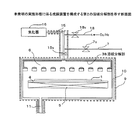
第1の方法は、例えば図10に示すような成膜装置によって実施される。
図10に示すCVD装置の成膜チャンバー101には、ヒータ102により加熱されるガス配管103,103a〜103c及びガス混合器104を介して複数の原料容器105a〜105cが接続されている。また、原料容器105a〜105cのそれぞれには、マスフローコントローラ106a〜106cを介してキャリアガス配管107a〜107cが接続されている。マスフローコントローラ106a〜106c、原料容器105a〜105c等のガス搬送系の装置は、恒温槽108a、108bに囲まれて所定の温度に加熱される。
The first method is performed by a film forming apparatus as shown in FIG. 10, for example.
A plurality of
複数の原料容器105a〜105cのそれぞれに充填される原料109a〜109cとして有機金属化合物を用いる。そして、図11Aに示すように、原料109a(109b、109c)は、原料容器105a(105b、105c)内で上下をメッシュ板110a、110bに挟まれた囲まれた領域に充填される。
An organometallic compound is used as the
原料容器105a〜105c、キャリアガス配管107a〜107cを含むガス供給系の装置は、恒温槽108a,108b及びヒータ102によって有機金属化合物の昇華温度以上の温度、例えば250℃に加熱される。
The gas supply system apparatus including the
これにより原料容器105a〜105c内で昇華した有機金属化合物は、キャリアガスとともに成膜チャンバー101内のシャワーヘッド111に導入される。なお、キャリアガスの流量はマスフローコントローラ106a〜106cにより制御される。
原料容器に充填した有機金属化合物を恒温槽で昇華して基板に供給する方法については、例えば特開2001−342566(特許文献1)に記載がある。
Thus, the organometallic compound sublimated in the
For example, JP-A-2001-342566 (Patent Document 1) describes a method of sublimating an organometallic compound filled in a raw material container in a thermostatic bath and supplying the substrate to a substrate.
シャワーヘッド111に導入された各有機金属化合物は、ヒータ112により加熱された基板113に飛来する。そして、基板113に供給された各有機金属化合物は、ガス配管103の途中で導入された酸化剤との反応により基板113上にPZT膜を形成する。基板113の温度は、ヒータ112により450℃〜600℃の温度範囲内となるように制御される。
Each organometallic compound introduced into the shower head 111 flies to the
なお、成膜チャンバー101に取り付けられた排気管114には自動圧力制御器115が取り付けられていて、自動圧力制御器115は、成膜チャンバー101に接続された圧力計116の測定データに基づいて排気流量を制御する。
なお、図10において、符号107a〜107m、118はバルブを示している。
Note that an
In FIG. 10,
図10に示す成膜装置を用いる成膜方法によれば、原料容器105a〜105c内で各有機金属化合物109a〜109cを昇華してキャリアガスとともに成膜チャンバー101に搬送する原料供給方法を採用している。
According to the film forming method using the film forming apparatus shown in FIG. 10, a raw material supply method is adopted in which the
この原料供給方法によれば、原料容器105a〜105c内で有機金属化合物を昇華させる時間が経過するにつれて、初期状態で微粉末状態の有機金属化合物109a〜109cが凝集して図11Bに示す状態となる。凝集が生じた有機金属化合物109a〜109cは、総表面積が小さくなり昇華量が減少するとともに、キャリアガスとの接触面積も小さくなり、有機金属化合物ガスの供給量が低下する。
According to this raw material supply method, as the time for sublimating the organometallic compound in the
そのような凝集は、PZTを形成する場合にZrを供給するための有機金属化合物で顕著に現れる。これは、Zr(DPM)4が、他の有機金属化合物であるPb(DPM)2とTi(OiPr)2(DPM)2よりも蒸気圧が低いからである。
この結果、成膜チャンバーに供給されるZrの濃度が使用時間の経過とともに変化しやすくなり、PZT膜の膜質を低下させる原因となる。
Such agglomeration is noticeable in the organometallic compound for supplying Zr when forming PZT. This is because Zr (DPM) 4 has a lower vapor pressure than Pb (DPM) 2 and Ti (OiPr) 2 (DPM) 2 which are other organometallic compounds.
As a result, the concentration of Zr supplied to the film forming chamber is likely to change with the passage of time of use, which causes the quality of the PZT film to deteriorate.
これに対し、第2の方法を実施するための成膜装置は、特に図示しないが、有機金属化合物を有機溶剤に溶解した液体原料を気化器により気化し、気化した原料をガス配管を通して成膜チャンバーに供給する構成となっている。そのような液体原料が充填された原料容器内では、有機金属化合物の凝集は殆ど問題にならない。 On the other hand, a film forming apparatus for carrying out the second method is not particularly shown, but a liquid raw material in which an organometallic compound is dissolved in an organic solvent is vaporized by a vaporizer, and the vaporized raw material is formed through a gas pipe. It is configured to supply to the chamber. In the raw material container filled with such a liquid raw material, the aggregation of the organometallic compound is hardly a problem.
しかし、有機溶剤を含む有機金属化合物を気化した原料ガスを基板上に供給してPZT膜を形成すると、有機溶剤の膜質への影響が無視できない状態となる。 However, when a source gas obtained by vaporizing an organometallic compound containing an organic solvent is supplied onto the substrate to form a PZT film, the influence of the organic solvent on the film quality cannot be ignored.
有機溶剤を除去する方法として、特開2002−305194号公報(特許文献2)には、成膜チャンバーに原料ガスを供給するガス配管の途中に燃焼室を設けて、その燃焼室に酸化剤を導入して原料ガスを320℃以上で予備加熱することが記載されている。これにより、基板への有機溶剤の供給を抑制することができると特許文献2に記載されている。
As a method for removing the organic solvent, Japanese Patent Laid-Open No. 2002-305194 (Patent Document 2) discloses that a combustion chamber is provided in the middle of a gas pipe for supplying a raw material gas to a film forming chamber, and an oxidizing agent is added to the combustion chamber. It is described that the raw material gas is introduced and preheated at 320 ° C. or higher. Thus,
また、特開2004−335607号公報(特許文献3)には、PZT、SBT等を形成するための原料ガスに酸素を添加する前に、ロジウム、又はロジウムを主成分とする貴金属の触媒により有機溶剤成分を加熱分解する触媒加熱分解手段を成膜チャンバーの上流側に設けることが記載されている。
しかし、特許文献2に記載の有機溶剤の除去方法によれば、原料ガスに含まれる有機金属化合物も同時に320℃以上で加熱されるので、有機金属化合物が基板に到達する前に分解してしまうおそれがある。
また、特許文献3には、有機溶媒成分の加熱分解について温度等の具体的な記載はなく、低温で分解できるとだけ記載されている。
However, according to the method for removing an organic solvent described in
Further, Patent Document 3 does not specifically describe the temperature or the like for the thermal decomposition of the organic solvent component, but only describes that it can be decomposed at a low temperature.
本発明の目的は、原料ガス中の有機溶媒成分を効率よく除去することができる成膜方法、成膜装置及び半導体装置の製造方法を提供することにある。 An object of the present invention is to provide a film forming method, a film forming apparatus, and a semiconductor device manufacturing method capable of efficiently removing an organic solvent component in a source gas.
本発明の1つの観点によれば、金属有機化合物を有機溶媒に溶解した溶液を気化して原料ガスを生成する工程と、原料ガスを、基板の設置された反応室内に導入する工程と、を有し、原料ガスが前記基板に到達する前に、貴金属を含む触媒と原料ガスと酸素ガスとを接触させ、有機溶媒を分解した上で、基板上に金属を含む膜を成膜することを特徴とする成膜方法が提供される。
本発明の別の観点によれば、基板が設置される反応室と、金属有機化合物を有機溶媒に溶解した溶液を気化して原料ガスを生成する気化器と、気化器で生成された原料ガスを反応室に導入する通路と、通路内に、酸素ガスを供給する酸素ガス供給部と、原料ガス中の有機溶媒と酸素ガスと貴金属を含む触媒とを接触させ、有機溶媒を分解する溶媒分解部とを有することを特徴とする成膜装置が提供される。
本発明の別の観点によれば、半導体基板の上方に下部電極を形成する工程と、下部電極上に誘電体膜を形成する工程と、誘電体膜上に上部電極を形成する工程と、を有し、前記誘電体膜を形成する工程は、金属有機化合物を有機溶媒に溶解した溶液を気化して原料ガスを生成し、下部電極の形成された半導体基板に供給する工程を含み、原料ガスが前記下部電極の形成された半導体基板に到達する前に、貴金属を含む触媒と原料ガスと酸素ガスとを接触させ、有機溶媒を分解して誘電体膜を堆積することを特徴とする半導体装置の製造方法が提供される。
According to one aspect of the present invention, a step of generating a raw material gas by vaporizing a solution in which a metal organic compound is dissolved in an organic solvent, and a step of introducing the raw material gas into a reaction chamber in which a substrate is installed. And before the source gas reaches the substrate, the catalyst containing the noble metal, the source gas, and the oxygen gas are brought into contact with each other, the organic solvent is decomposed, and a film containing the metal is formed on the substrate. A featured deposition method is provided.
According to another aspect of the present invention, a reaction chamber in which a substrate is installed, a vaporizer that generates a raw material gas by vaporizing a solution obtained by dissolving a metal organic compound in an organic solvent, and a raw material gas generated by the vaporizer Solvent decomposition that decomposes the organic solvent by bringing the oxygen gas supply unit that supplies oxygen gas into the reaction chamber, the organic solvent in the raw material gas, the catalyst containing the oxygen gas, and the noble metal in contact with each other A film forming apparatus characterized in that the film forming apparatus is provided.
According to another aspect of the present invention, a step of forming a lower electrode above a semiconductor substrate, a step of forming a dielectric film on the lower electrode, and a step of forming an upper electrode on the dielectric film, And forming the dielectric film includes a step of generating a source gas by vaporizing a solution in which a metal organic compound is dissolved in an organic solvent, and supplying the source gas to the semiconductor substrate on which the lower electrode is formed. Before reaching the semiconductor substrate on which the lower electrode is formed, a catalyst containing a noble metal, a source gas, and an oxygen gas are brought into contact with each other to decompose an organic solvent and deposit a dielectric film. A manufacturing method is provided.
本発明によれば、有機溶媒を含む膜形成用原料ガスと酸素ガスと触媒を接触させることにより、原料ガスに含まれる有機溶媒を効率よく分解することができる。 According to the present invention, the organic solvent contained in the raw material gas can be efficiently decomposed by bringing the film forming raw material gas containing the organic solvent into contact with the oxygen gas and the catalyst.
以下に、本発明の実施形態を図面に基づいて詳細に説明する。
図1は、本発明の実施形態に係る成膜装置の一例を示す構成図である。
Embodiments of the present invention will be described below in detail with reference to the drawings.
FIG. 1 is a configuration diagram showing an example of a film forming apparatus according to an embodiment of the present invention.
図1に示す成膜装置は、有機金属化合物を原料に用いてCVD法により膜を形成する装置であって、成膜チャンバー10内には、基板1を載置するウェーハステージ4と、基板1を加熱するヒータ5と、ウェーハステージ4の上方に配置されたシャワーヘッド6とを有している。
The film forming apparatus shown in FIG. 1 is an apparatus for forming a film by a CVD method using an organometallic compound as a raw material. In a
シャワーヘッド6は、成膜チャンバー10の上部のガス導入ポート10aから導入するガスを拡散しつつ多数の孔を通してムラなく基板1に供給する構造を有するガス分散装置であり、シャワーノズルともいう。
The shower head 6 is a gas dispersion apparatus having a structure in which a gas introduced from a
また、成膜チャンバー10の下部には、排気管11を介して外部の真空ポンプ12に接続される排気ポート10bが設けられている。排気管11には、成膜チャンバー10に取り付けられた圧力計13の測定値に基づいて排気量を制御する自動圧力制御器(APC:Auto Pressure Controller)14が設けられている。
In addition, an
成膜チャンバー10のガス導入ポート10aは、第1のガス配管15を介して気化器16のガス放出ポートに接続される。また、第1のガス配管15のうち成膜チャンバー10寄りには第1のバルブ15vが接続され、さらにバルブ15vより上流側には、排気管11に繋がるバイパス配管7が接続されている。
The
バイパス配管7には第2のバルブ7vが取り付けられており、第1のガス配管15を流れるガスの流路は、第1、第2のバルブ15v,7vの操作によって成膜チャンバー10かバイパス配管7のいずれかを選択することが可能になっている。
A
第1のガス配管15のうちバイパス配管7との接続部より上流側には、第2のガス配管18aを介して酸化剤供給源18が接続されている。酸化剤供給源18から供給される酸化剤(酸化ガス)として、例えば、酸素(O2)、オゾン(O3)、一酸化窒素(N2O)、二酸化窒素(NO2)のうち少なくとも1つのガスが使用され、以下の説明では酸化剤として、酸素ガスを例に挙げる。なお、第2のガス配管18aには、バルブ(不図示)を介して水素ガス源が接続され、酸化ガスを水素ガスに切替えることが可能になっている。
An
第1のガス配管15と第2のガス配管18aとバイパス配管7とそれらの接続部分はそれぞれステンレスから形成されている。なお、第2のガス配管18aにはバルブ18vが取り付けられている。
The
第1のガス配管15のうち第2のガス配管18aとの接続部分よりも下流側、即ち成膜チャンバー10寄りの領域には、有機溶媒を分解するための溶媒分解部8が設けられている。
A solvent
溶媒分解部8は、例えば図2に示すような断面構造のように、少なくとも第2のガス配管18aよりも成膜チャンバー10寄りの領域の内面に形成された触媒膜8aを有している。触媒膜8としては、プラチナ(Pt)、イリジウム(Ir)等のような貴金属を有する膜からなる触媒が形成されている。なお、以下の説明では触媒としてPtを例に挙げて説明する。
The solvent
プラチナ、イリジウム等の貴金属またはその酸化物は、例えば強誘電体キャパシタの電極を構成する材料であって、成膜チャンバー10内の基板1上に下部電極としてCVD法により形成されることもある。
A noble metal such as platinum or iridium or an oxide thereof is, for example, a material constituting an electrode of a ferroelectric capacitor, and may be formed on the
溶媒分解部8は、第1のガス配管15を通して流入する有機溶媒と酸素ガスの双方を触媒に接触させることにより有機溶媒を燃焼反応により分解する。その詳細については後述する。
The
気化器16は、原料導入ポートから導入した液体原料を気化してガス排出ポートから第1のガス配管15に放出する装置であり、キャリアガスとともに導入した液体原料を霧化して気化チャンバー16a内に放出する気化ノズル16bと、気化チャンバー16aを液体原料の気化温度に予め加熱し且つ保温するヒータ16cとを有している。
The
気化チャンバー16aの温度は、有機金属化合物を含む液体原料を気化する際に吸熱作用により低下し易いので、これを防止するために熱容量を稼げるステンレスなどの材質で気化チャンバー16aを構成する。
Since the temperature of the
気化チャンバー16a内の圧力は、気化したガスの搬送先となる成膜チャンバー10内の圧力にも影響されるが、気化ノズル16bに導入する液体原料の流量及びキャリアガス流量によって制御される。なお、特に図示しないが、気化器16には、気化チャンバー16aの圧力を測定する圧力計が取り付けられている。
The pressure in the
気化ノズル16bには、第3のガス配管19と第1の給液管21が接続されている。第3のガス配管19の上流側には、アルゴン(Ar)、窒素(N2)等のキャリアガスを気化ノズル16bに供給するためのキャリアガス源20が接続されている。また、第1の給液管21の上流側には、気化ノズル16bに液体原料を供給するマニホールド17の原料出力ポートが接続されている。なお、第3のガス配管19にはバルブ19vが取り付けられている。
A
マニホールド17は、原料導入ポートに並列に接続された第2〜第6の給液管22a〜22eから導入する液体原料を混合して原料放出ポートから放出する構造を有するとともに、液体原料の気化温度より低い温度に内部を加熱するヒータ17aを有している。
The manifold 17 has a structure in which liquid raw materials introduced from second to sixth
第1の給液管21、第1、第3のガス管15、19及び成膜チャンバー10等にはヒータ9が設けられ、気化した有機金属化合物の凝集を防止している。ヒータ9は、温度分布制御が可能な構造を有し、通常220℃〜280℃に設定されるが、第1のガス配管15のうち少なくとも第2のガス配管18aの接続部より下流側の領域では加熱温度を300℃〜350℃まで上昇可能になっている。
The first
マニホールド17の原料入力ポートに接続される第2〜第6の給液管22a〜22eのそれぞれは、液体用のマスフローコントローラ(MFC)23a〜23eを介して第1〜第5の原料容器24〜28に接続されている。
Each of the second to sixth
また、第1〜第5の原料容器24〜28のそれぞれの上部に形成される空間には、ネオン、窒素、アルゴン等の不活性ガスを封入した不活性ガス源30に接続される不活性ガス導入管31a〜31eが差し込まれている。
Moreover, the inert gas connected to the inert gas source 30 which enclosed inert gas, such as neon, nitrogen, and argon, in the space formed in each upper part of the 1st-5th raw material containers 24-28. The
第1〜第5の原料容器24〜28のそれぞれに充填された液体原料には、第2〜第6の給液管22a〜22eが差し込まれている。これにより、第1〜第5の原料容器24〜28内に充填された液体原料は、不活性ガスの供給により、第2〜第6の給液管22a〜22eを介してマニホールド17に圧送されることになる。
Second to sixth
第1〜第5の原料容器24〜28のそれぞれは、密封状態で液体原料を収納する容器であって、その液体原料に対して耐腐食性が優れるステンレスなどの材料から構成されている。第1〜第5の原料容器24〜28に付随する第2〜第6の給液管22a〜22e、不活性ガス導入管31a〜31eの他、Oリング、ガスケット及びバルブ等も同様にステンレスから構成される。
Each of the first to fifth raw material containers 24 to 28 is a container for storing a liquid raw material in a sealed state, and is made of a material such as stainless steel having excellent corrosion resistance against the liquid raw material. In addition to the second to sixth
なお、図中符号34a〜34pは、第2〜第7の給液管22a〜22eに接続されるバルブを示し、符号35a〜35fは、不活性ガス導入管31a〜31eのそれぞれに接続されるバルブを示している。
In addition, the code |
ところで、上記の溶媒分解部8は、第1のガス配管15の内面に形成された貴金属を含む触媒膜8aから構成されている。その触媒膜8aは、メッキ法により形成してもよいしCVD法により形成してもよい。
By the way, the solvent decomposing
CVD法により形成する場合には例えば次のような方法を採用する。
まず、触媒作用を有する金属と有機化合物との金属錯体を含む有機金属化合物、より具体的にはPt(HFA)2を原料とし、これを有機溶媒に溶解して構成されるPt用CVD原料を第5の原料容器28に充填する。Pt(HFA)2に示すHFAはヘキサフルオロアセトン(hexafluoroacetone)である。
In the case of forming by the CVD method, for example, the following method is adopted.
First, an organic metal compound containing a metal complex of a metal having a catalytic action and an organic compound, more specifically, a Pt CVD raw material composed of Pt (HFA) 2 as a raw material and dissolved in an organic solvent. The fifth
プラチナ(Pt)を成膜するための有機金属化合物として、Pt(HFA)2の他にPt(DPM)2等があるが、以下の説明ではPt(HFA)2を例に挙げている。なお、Pt(DPM)2に示すDPMの化学式は(CH3)3C-CO-CH-CO-C(CH3)3である。
また、有機溶媒として、テトラヒドロフラン(以下、THFとも記載する)、或いは酢酸ブチル(以下、n−Baとも記載する)、オクタン等を使用し、以下の説明では酢酸ブチルを使用することを例に挙げている。
As an organometallic compound for depositing platinum (Pt), there is Pt (DPM) 2 in addition to Pt (HFA) 2. In the following description, Pt (HFA) 2 is taken as an example. Note that the chemical formula of DPM shown in Pt (DPM) 2 is (CH 3 ) 3 C—CO—CH—CO—C (CH 3 ) 3 .
Further, as an organic solvent, tetrahydrofuran (hereinafter also referred to as THF), butyl acetate (hereinafter also referred to as n-Ba), octane or the like is used, and in the following description, butyl acetate is used as an example. ing.
そのPt用CVD原料におけるPt濃度は、酢酸ブチルにおける飽和溶解度以下とする。具体的には、Pt(HFA)2濃度を0.1モル/リットル(mol/l)〜3.0mol/lの濃度範囲に調整すること望ましい。
また、第4の原料容器27には有機溶剤を充填する。
The Pt concentration in the Pt CVD raw material is set to be equal to or lower than the saturation solubility in butyl acetate. Specifically, it is desirable to adjust the Pt (HFA) 2 concentration to a concentration range of 0.1 mol / liter (mol / l) to 3.0 mol / l.
The fourth
まず、第5の原料容器28に充填されたPt用CVD原料は、不活性ガス源30から供給される不活性ガス、例えばヘリウムガスにより第5の給液管22eに圧送され、さらにマスフローコントローラ23e及びマニホールド17を介して気化器16に送られる。アルゴン、ヘリウム等の不活性ガスは酢酸ブチルへの溶解度が小さいので問題はない。
First, the Pt CVD raw material filled in the fifth
第1の給液管21でのPt用CVD原料の流量は、マスフローコントローラ23eにより制御され、気化器16の気化能力、第1のガス配管15でのガス流量などの条件によって決定される。
The flow rate of the Pt CVD raw material in the first
気化器16内では、Pt用CVD原料は気化ノズル16bから不活性ガスとともに噴霧され、さらに気化チャンバー16a内で気化され第1のガス配管15に搬送される。第1のガス配管15は、第2のガス配管18aの接続部分より上流側でヒータ9によって予めPt(HFA)2の気化温度より高い温度に加熱されている。酢酸ブチルは、Pt(HFA)2の気化温度により気化する。
なお、Ptを含む有機金属原料を気化するための気化器を、他の有機金属原料を気化するための気化器とは別に設けてもよい。
In the
Note that a vaporizer for vaporizing an organometallic raw material containing Pt may be provided separately from a vaporizer for vaporizing other organometallic raw materials.
そして、図2に示すように、ガス流路に沿って温度分布の制御が可能なヒータ9により、第1のガス配管15のうち少なくとも第2のガス配管との接続部分より下流側を、気化温度より高い300℃〜350℃に加熱する。具体的には、例えば、第2の配管18aの接続部分とバイパス配管7の接続部分との間の第1領域15aを300℃とし、さらにバイパス配管7より下流側の第2領域15bを350℃とし、第2領域15bと第1領域15aの間の第3領域15cとその他の領域15eをPt用CVD原料の気化温度に設定する。
Then, as shown in FIG. 2, the
これにより、第1のガス配管15内を流れるPt(DPM)2は、第1、第2領域15a,15bで分解して第1のガス配管15の内面にPtからなる触媒膜8aを形成する。
この方法により形成されたPtを有する触媒膜8aは炭素を含んでいる。その炭素は、Pt(HFA)2と酢酸ブチルの反応による分解物である。触媒膜8aに残留する炭素は、触媒作用には寄与しないので除去することが望ましい。
Thus, Pt (DPM) 2 flowing in the
The catalyst film 8a having Pt formed by this method contains carbon. The carbon is a decomposition product of the reaction of Pt (HFA) 2 and butyl acetate. It is desirable to remove carbon remaining in the catalyst film 8a because it does not contribute to the catalytic action.
残留炭素の除去方法として、Ptの触媒膜8aを被覆した第1のガス配管15内に水素(H2)ガスを流す方法がある。水素ガスを触媒膜8aの表面に供給することにより、蒸気圧を有する炭化水素(CHx)が形成されて触媒膜8a中から炭素が除外される。この際、CHxの生成を促進するために第1のガス配管15を例えば350℃程度で加熱することが望ましい。なお、水素ガスは、第2のガス配管18aから供給してもよい。
As a method for removing residual carbon, there is a method of flowing hydrogen (H 2 ) gas into the
以上のような方法により、第1のガス配管15のうち酸化ガス導入部よりも下流側の内面に触媒膜8aが形成される。
次に、溶媒分解部8を備えた成膜装置を使用して基板1上にPZT膜2を形成する方法について説明する。
By the above method, the catalyst film 8a is formed on the inner surface of the
Next, a method for forming the
まず、Pb(DMHD)2を酢酸ブチルに溶解させて液化した第1のCVD原料を第1の原料容器24の中に充填し、また、Zr(DMHD)4を酢酸ブチルに溶解させて液化した第2のCVD原料を第2の原料容器25の中に充填し、Ti(OiPr)2(DPM)2を酢酸ブチルに溶解させて液化した第3のCVD原料を第3の原料容器26の中に充填し、第4の原料容器27の中に有機溶剤として酢酸ブチルを充填する。
Pb(DMHD)2、Zr(DMHD)4、Ti(OiPr)2(DPM)2はそれぞれ金属と有機化合物との金属錯体を含む有機金属化合物である。Pb(DMHD)2、Zr(DMHD)4に示すDMHDの化学式は(CH3)2CHCOCHCOCH(CH3)2である。Ti(OiPr)2(DPM)2の代わりにTi(O iPr)2(DMHD)2を使用しても効果は同じである。
First, the first CVD raw material in which Pb (DMHD) 2 was dissolved in butyl acetate and liquefied was filled in the first raw material container 24, and Zr (DMHD) 4 was dissolved in butyl acetate and liquefied. The second CVD source is filled in the second source vessel 25, and the third CVD source obtained by dissolving Ti (OiPr) 2 (DPM) 2 in butyl acetate is liquefied in the
Pb (DMHD) 2 , Zr (DMHD) 4 , and Ti (OiPr) 2 (DPM) 2 are each an organometallic compound containing a metal complex of a metal and an organic compound. The chemical formula of DMHD shown in Pb (DMHD) 2 and Zr (DMHD) 4 is (CH 3 ) 2 CHCOCHCOCH (CH 3 ) 2 . Even if Ti (O iPr) 2 (DMHD) 2 is used instead of Ti (OiPr) 2 (DPM) 2 , the effect is the same.
そして、第1のCVD原料中のPb(DMHD)2の濃度、第2のCVD原料中のZr(DMHD)4の濃度、および第3のCVD原料中のTi(OiPr)2(DPM)2の濃度をそれぞれ0.5mol/l〜1.0mol/lの範囲で調整する。 The concentration of Pb (DMHD) 2 in the first CVD material, the concentration of Zr (DMHD) 4 in the second CVD material, and Ti (OiPr) 2 (DPM) 2 in the third CVD material The concentration is adjusted in the range of 0.5 mol / l to 1.0 mol / l, respectively.
Pb(DMHD)2、Zr(DMHD)4、Ti(OiPr)2(DPM)2のそれぞれの有機金属化合物は室温において白色の固体であって微粉末状になっている。 Each organometallic compound of Pb (DMHD) 2 , Zr (DMHD) 4 , and Ti (OiPr) 2 (DPM) 2 is a white solid at room temperature and is in a fine powder form.
PZT膜を形成するために用いる有機溶剤としてはテトラヒドロフラン或いは酢酸ブチルのどちらの有機溶剤を選択しても同じ効果を得ることができる。 The same effect can be obtained by selecting either tetrahydrofuran or butyl acetate as the organic solvent used for forming the PZT film.
PZT膜を形成するために、まず、不活性ガスを第1〜第4の原料容器24〜27に充填することにより、それらの内部空間の圧力を高くし、さらに、第2〜第5の給液管22a〜22dにそれぞれ接続されたバルブ34a〜34pを制御することにより、第1〜第3の原料容器24〜26内のCVD原料と第4の原料容器28内の有機溶剤をマニホールド17に圧送する。
In order to form a PZT film, first, the first to fourth raw material containers 24 to 27 are filled with an inert gas to increase the pressure in the internal space, and further, the second to fifth supply gas is supplied. By controlling the
これにより、第1〜第3のCVD原料は有機溶剤とともにマニホールド17内で混合され、さらに第1の給液管21を通して気化器16に搬送される。
第1の給液管21での液体原料の流量は、気化器16の気化能力、成膜チャンバー10へのガス流量などの条件によって決定され、マスフローコントローラ23a〜23eにより制御される。
Thereby, the first to third CVD raw materials are mixed in the manifold 17 together with the organic solvent, and further conveyed to the
The flow rate of the liquid raw material in the first
そしてマニホールド17から圧送された第1〜第3のCVD原料及び有機溶剤はキャリアガスとともに気化ノズル16bから気化チャンバー16a内に噴霧され、さらに霧化された第1〜第3のCVD原料及び有機溶剤は、ヒータ16cによって気化されてCVD原料ガスとなる。
The first to third CVD raw materials and organic solvent pumped from the manifold 17 are sprayed into the vaporizing
その気化条件として、気化チャンバー16a内での温度を220℃〜280℃、好ましくは250℃〜270℃の範囲内に設定し、また、気化チャンバー16a内での気化圧力を20Torr(2666.4Pa)以下に設定する。温度制御はヒータ16cによって行われる。
気化圧力は、成膜チャンバー10の圧力に影響されるが、第1〜第3のCVD原料の流量、キャリアガスの流量などの調整によって制御される。
As the vaporization conditions, the temperature in the
The vaporization pressure is influenced by the pressure in the
気化器16において気化されたCVD原料は、キャリアガスとともに第1のガス配管15に搬送され、さらに、第1のガス配管15の途中で酸化剤供給源18から酸素ガスが加えられて溶媒分解部8を通過する。第1のガス配管15はヒータ9によって220℃〜280℃の範囲に加熱される。
なお、酸素ガスの流量は、溶媒分解部8を有しない従来の成膜装置における流量よりも多くする。
The CVD raw material vaporized in the
The flow rate of the oxygen gas is set higher than that in a conventional film forming apparatus that does not have the solvent
溶媒分解部8では、CVD原料ガス中の酢酸ブチルは酸素と燃焼反応を生じて分解する。その燃焼反応はさらに溶媒分解部8内の触媒膜8aによって促進される。この場合、溶媒分解部8は、第1のガス配管15の他の領域と同じ温度、即ち280℃以下、220℃以上の範囲に設定される。なお、溶媒分解部8における触媒作用の詳細については後述する。
In the
このように有機溶媒成分が低減されたCVD原料ガスと酸素ガスは、第1のガス配管15からシャワーヘッド6内に流入してその中で拡散し、さらに基板1に向けて放出される。
Thus, the CVD source gas and oxygen gas with reduced organic solvent components flow into the shower head 6 from the
これにより、CVD原料ガスと酸化ガスは基板1表面にムラ無く到達し、そこで反応及び分解を繰り返すことによりPZT膜2が基板1上に形成される。なお、イリジウム或いは酸化イリジウム、プラチナ或いはプラチナ酸化物からなる膜が基板1の表面に形成されている場合には、PZT膜2の結晶は(111)優先配向性を示す。
Thereby, the CVD source gas and the oxidizing gas reach the surface of the
なお、PZT膜2の成膜終了後には、第1のガス配管15内を流れるガスは、開閉バルブ15v、7vの切り替えにより流路が変更されてバイパス配管7を通して排気管11に搬送される。
After the formation of the
次に、本実施形態に係る成膜装置を使用して形成されたPZT膜から構成される強誘電体キャパシタと、従来技術の成膜装置を使用して形成されたPZT膜から構成される強誘電体キャパシタとを比較する。 Next, a ferroelectric capacitor composed of a PZT film formed using the film forming apparatus according to the present embodiment and a strong capacitor composed of a PZT film formed using the conventional film forming apparatus. The dielectric capacitor is compared.
強誘電体キャパシタにおいては、誘電体膜であるPZT膜を薄膜化すればするほど容量が増加傾向となるのが理想的である。しかし、PZT膜を薄くしても容量が増加しないこともあり、この場合には、強誘電体キャパシタの微細化を図るために、少なくともPZT膜の薄膜化に伴ってキャパシタ容量が減少しないことが好ましい。 In a ferroelectric capacitor, ideally, the capacity tends to increase as the PZT film, which is a dielectric film, is made thinner. However, even if the PZT film is thinned, the capacitance may not increase. In this case, in order to miniaturize the ferroelectric capacitor, the capacitor capacity may not decrease at least as the PZT film is thinned. preferable.
図1に示した本実施形態の成膜装置を使用し、酸素ガスが加えられたCVD原料ガスを溶媒分解部8に通過させて基板1に供給してPZT膜2を形成し、PZT膜の厚さと強誘電体キャパシタの容量との関係を調べたところ図3の実線に示すような特性が得られた。
Using the film forming apparatus of the present embodiment shown in FIG. 1, a CVD source gas to which oxygen gas is added is passed through the
その特性によれば、120nmから80nmにPZT膜を薄くしてもキャパシタ容量は殆ど変化せず、また、80nmから60nmに薄くするとキャパシタ容量が減少するがその量は僅かである。これにより、本実施形態の成膜方法を強誘電体キャパシタの製造工程に適用することによりキャパシタ容量の低下の抑制が可能になる。
なお、図3における縦軸に示すキャパシタ容量は、PZT膜の厚さを120nmとした場合のキャパシタ容量(単位:μC/cm2)を「1」として規格化した値である。
According to the characteristics, even if the thickness of the PZT film is reduced from 120 nm to 80 nm, the capacitance of the capacitor hardly changes, and when the thickness is reduced from 80 nm to 60 nm, the capacitance of the capacitor decreases but the amount is small. As a result, it is possible to suppress a decrease in the capacitance of the capacitor by applying the film forming method of the present embodiment to the manufacturing process of the ferroelectric capacitor.
Note that the capacitor capacity shown on the vertical axis in FIG. 3 is a value normalized by assuming that the capacitor capacity (unit: μC / cm 2 ) when the thickness of the PZT film is 120 nm is “1”.
一方、図10に示した従来の成膜装置を使用し、有機金属化合物を加熱して昇華させた原料ガスを基板に供給してPZT膜を形成したところ、PZT膜の厚さとキャパシタ容量との関係は図3の破線に示すような特性となった。
その特性によれば、本実施形態と同様に、PZT膜の厚さを120nmから60nmまで薄くしてもキャパシタ容量は殆ど変化しない。
On the other hand, when the conventional deposition apparatus shown in FIG. 10 was used and the PZT film was formed by supplying the substrate with the source gas obtained by heating and sublimating the organometallic compound, the relationship between the thickness of the PZT film and the capacitance of the capacitor was obtained. The relationship was as shown by the broken line in FIG.
According to the characteristics, as in the present embodiment, the capacitance of the capacitor hardly changes even if the thickness of the PZT film is reduced from 120 nm to 60 nm.
これに対して、溶媒分解部8の無い状態で構成される従来の成膜装置を用いて、酸素ガスが加えられたCVD原料ガスを基板に供給してPZT膜を形成したところ、PZT膜の厚さと強誘電体キャパシタの容量との関係は図3の一点鎖線に示すような特性となった。
On the other hand, when a PZT film was formed by supplying a CVD source gas to which oxygen gas was added to a substrate using a conventional film forming apparatus configured without the
その特性によれば、PZTの膜厚を120nmから100nmまで薄くしてもキャパシタ容量は殆ど変化しないが、その膜厚を100nmから薄くするにつれてキャパシタ容量が大幅に低下してしまい強誘電体キャパシタの微細化には向かない特性となっている。 According to the characteristics, even if the thickness of the PZT film is reduced from 120 nm to 100 nm, the capacitance of the capacitor hardly changes. However, as the thickness of the PZT film is reduced from 100 nm, the capacitance of the capacitor is greatly reduced, and the ferroelectric capacitor is reduced. This is not suitable for miniaturization.
以上のことから、CVD原料ガスに酸素を加えて溶媒分解部8で有機溶媒を分解した原料ガスによって膜質の良いPZT膜を形成でき、これによりPZT膜の薄層化に伴うキャパシタ容量の低下を抑制できることが明らかになった。
From the above, it is possible to form a PZT film with good film quality by using the source gas obtained by adding oxygen to the CVD source gas and decomposing the organic solvent in the
また、有機金属化合物を昇華して得られた原料ガスを使用してPZT膜を形成しても、PZT膜の薄層化に伴うキャパシタ容量の低下を抑制できる。しかし、この成膜方法によれば、図4の破線で示すように、成膜チャンバーでの基板の累積処理枚数が増えるにつれてキャパシタ容量が低下するので、量産性が劣る。これは、背景技術の欄で説明したように、原料容器内で有機金属化合物の凝集が生じるからである。 Moreover, even if the PZT film is formed using the raw material gas obtained by sublimating the organometallic compound, it is possible to suppress the decrease in the capacitor capacity accompanying the thinning of the PZT film. However, according to this film forming method, as shown by the broken line in FIG. 4, the capacity of the capacitor decreases as the cumulative number of substrates processed in the film forming chamber increases, so that the mass productivity is inferior. This is because the organic metal compound aggregates in the raw material container as described in the background art section.
有機金属化合物を有機溶媒に溶解して形成されたCVD原料を使用する場合には、図4の一点鎖線で示すように、成膜チャンバーでの基板の累積処理枚数が150枚となってもキャパシタ容量に大きな変化はない。これにより、CVD原料を成膜チャンバーに安定して供給できることがわかる。 When using a CVD raw material formed by dissolving an organometallic compound in an organic solvent, as shown by the one-dot chain line in FIG. There is no significant change in capacity. Thereby, it can be seen that the CVD raw material can be stably supplied to the film forming chamber.
次に、本実施形態に係る成膜装置の溶媒分解部8における有機溶媒の燃焼について説明する。
まず、触媒膜を基板上に形成し、その基板を真空チャンバー内に置き、さらに基板に熱電対を接続した。そして、真空チャンバー内で基板をヒータで加熱し、さらにガス配管を通して真空チャンバー内にガスを導入するとともに、排気管を通して真空チャンバー内部を減圧した。なお、触媒膜としてPtの変わりにIrを形成して実験を行ったが、どちらの材料でも触媒作用があるので違いはない。
Next, the combustion of the organic solvent in the
First, a catalyst film was formed on a substrate, the substrate was placed in a vacuum chamber, and a thermocouple was connected to the substrate. Then, the substrate was heated with a heater in the vacuum chamber, and gas was introduced into the vacuum chamber through the gas pipe, and the inside of the vacuum chamber was decompressed through the exhaust pipe. In addition, although it experimented by forming Ir instead of Pt as a catalyst film, since both materials have a catalytic action, there is no difference.
このような装置では、通常、基板加熱温度と基板表面温度は線形関係となる。
そこで、基板に酸素のみを供給した場合と、酢酸ブチルと酸素の混合ガスを基板に供給した場合のそれぞれについて、基板加熱温度を変化させて基板表面温度を調査したところ、図5に示すような関係が得られた。
In such an apparatus, the substrate heating temperature and the substrate surface temperature usually have a linear relationship.
Therefore, the substrate surface temperature was investigated by changing the substrate heating temperature for each of the case where only oxygen was supplied to the substrate and the case where the mixed gas of butyl acetate and oxygen was supplied to the substrate. As shown in FIG. A relationship was obtained.
図5の横軸と縦軸は、それぞれ基板加熱温度の値と基板上昇温度の値である。基板上昇温度は、熱電対により測定された基板温度と、ヒータの加熱温度との差を示している。 The horizontal and vertical axes in FIG. 5 are the substrate heating temperature value and the substrate rising temperature value, respectively. The substrate rising temperature indicates the difference between the substrate temperature measured by the thermocouple and the heating temperature of the heater.
酢酸ブチルと酸素のそれぞれのガス流量を1ccm、5slmとした。また、真空チャンバー内の圧力を1Torr(約133Pa)とした。さらに、基板加熱温度を100℃から300℃まで変化した。 The gas flow rates of butyl acetate and oxygen were 1 ccm and 5 slm, respectively. The pressure in the vacuum chamber was 1 Torr (about 133 Pa). Further, the substrate heating temperature was changed from 100 ° C. to 300 ° C.
図5の破線に示すように、酸素ガスのみを真空チャンバー内に導入した場合には、基板上昇温度は数度程度となった。即ち、加熱温度と基板表面温度の差は殆どなく、基板表面温度は、加熱温度とともに増加し、加熱温度に対して線形関係となっている。 As shown by a broken line in FIG. 5, when only oxygen gas was introduced into the vacuum chamber, the substrate rising temperature was about several degrees. That is, there is almost no difference between the heating temperature and the substrate surface temperature, and the substrate surface temperature increases with the heating temperature and has a linear relationship with the heating temperature.
これに対し、酸素と酢酸ブチルの混合ガスを真空チャンバーに導入すると、図5の実線に示すように、酸素のみの場合に比べて基板上昇温度は高くなり、しかも基板表面温度は基板加熱温度に対して線形関係にはなっていない。これは、酸素と酢酸ブチルの燃焼反応によるものである。 On the other hand, when a mixed gas of oxygen and butyl acetate is introduced into the vacuum chamber, as shown by the solid line in FIG. 5, the substrate rising temperature becomes higher than that of oxygen alone, and the substrate surface temperature becomes the substrate heating temperature. On the other hand, it is not a linear relationship. This is due to the combustion reaction of oxygen and butyl acetate.
また、酸素と酢酸ブチルの混合ガスを基板に供給する場合には、基板加熱温度を150℃以上にすると基板上昇温度も少しずつ高くなり、さらに基板加熱温度が200℃前後になると基板上昇温度はピークとなり、さらに基板加熱温度を約200℃から高くするにつれて基板上昇温度は徐々に低くなって300℃付近で基板加熱温度より少し高い状態となる。 Also, when supplying a mixed gas of oxygen and butyl acetate to the substrate, if the substrate heating temperature is set to 150 ° C. or higher, the substrate rising temperature gradually increases, and if the substrate heating temperature is about 200 ° C., the substrate rising temperature is As the substrate heating temperature is increased from about 200 ° C., the substrate rising temperature gradually decreases and becomes slightly higher than the substrate heating temperature around 300 ° C.
このように基板加熱温度が150℃以上になると基板上昇温度が急激に高くなるという現象は、Irの触媒作用が寄与するからである。即ち、酸素と酢酸ブチルの燃焼反応がIrの触媒作用により加速されて加熱温度以上に基板の温度が高くなるからである。 This is because the phenomenon that the substrate temperature rises rapidly when the substrate heating temperature is 150 ° C. or higher contributes to the catalytic action of Ir. That is, the combustion reaction of oxygen and butyl acetate is accelerated by the catalytic action of Ir, and the temperature of the substrate becomes higher than the heating temperature.
ところで、従来技術の欄に示した特開2004−335607号公報には、有機金属原料ガスに酸素を添加せずに、ロジウムの触媒により有機溶媒成分を加熱分解することが記載されている。しかし、この加熱分解では、酸素添加による燃焼反応を伴っていないので、触媒による燃焼反応の促進といった作用は生じない。また、ロジウムの触媒により有機溶媒成分を加熱分解する際には、基板測定温度と基板加熱温度はほぼ同じになる。 Incidentally, Japanese Patent Application Laid-Open No. 2004-335607 shown in the column of the prior art describes that an organic solvent component is thermally decomposed by a rhodium catalyst without adding oxygen to an organic metal source gas. However, since this thermal decomposition does not involve a combustion reaction due to the addition of oxygen, there is no effect of promoting the combustion reaction by the catalyst. When the organic solvent component is thermally decomposed with a rhodium catalyst, the substrate measurement temperature and the substrate heating temperature are substantially the same.
以上のように本実施形態の成膜方法及び成膜装置によれば、CVD原料ガスと酸素ガスと触媒を接触させると、有機金属化合物の分解温度以下の温度でも有機溶媒を分解することができる。この結果、PZT膜を形成する際の有機溶剤による影響を大幅に低減することができる。 As described above, according to the film forming method and film forming apparatus of this embodiment, when the CVD source gas, oxygen gas, and catalyst are brought into contact, the organic solvent can be decomposed even at a temperature lower than the decomposition temperature of the organometallic compound. . As a result, the influence of the organic solvent when forming the PZT film can be greatly reduced.
なお、上記した実施形態による成膜方法はPZT膜を形成するためにのみ適用されるものではなく、ランタン(La)、カルシウム(Ca)などのドーパントをPZTに添加したPZT系膜の形成についても適用できる。また、PZT以外の膜、例えばストロンチウム・ビスマス・タンタル酸化物(SBT)膜を形成する場合にも適用できる。 Note that the film forming method according to the above-described embodiment is not only applied for forming a PZT film, but also for forming a PZT-based film in which a dopant such as lanthanum (La) or calcium (Ca) is added to PZT. Applicable. The present invention can also be applied to the case of forming a film other than PZT, for example, a strontium bismuth tantalum oxide (SBT) film.
ところで、上記の溶媒分解部8は、第1のガス配管15の内面に形成された触媒膜8aから構成しているが、そのような構造に限られるものではない。例えば、溶媒分解部8を図6に示すようにシャワーヘッド6に設けてもよい。
図6に示すシャワーヘッド6は、その内面に触媒膜を被覆して構成される溶媒分解部38を併設した構造を有し、その触媒膜の形成方法は、図2に示した触媒膜8aの形成方法と同様の方法を採用する。
By the way, although said solvent decomposition |
The shower head 6 shown in FIG. 6 has a structure in which a solvent decomposition portion 38 configured by covering the inner surface of the shower head 6 is provided, and a method for forming the catalyst film is the same as that of the catalyst film 8a shown in FIG. A method similar to the forming method is employed.
即ち、気化器16と成膜チャンバー10を接続する第1のガス配管15及びバルブ15vをCVD原料の気化温度に設定するとともに、シャワーヘッド6をその気化温度より高い300℃〜350℃に加熱する。シャワーヘッド6の温度制御方法について、シャワーヘッド6にヒータが装備されている場合にはそのヒータによって前記温度に制御するが、ヒータを装備していない場合には基板加熱用のヒータ5を利用してヒータ5からの輻射熱によって300℃〜350℃の温度に制御する。
That is, the
そして、有機溶媒及びPt用有機金属化合物を含む原料ガスを気化器16から第1のガス配管15を通して成膜チャンバー10に導入する。Pt用有機金属化合物として例えばPt(HFA)2を使用する。この場合、第1のガス配管15の温度を280℃以下に設定することでその内面にPtを積極的に被覆しない。
Then, a source gas containing an organic solvent and an organometallic compound for Pt is introduced from the
成膜チャンバー10に導入された原料ガスは、シャワーヘッド6の内部において加熱分解してその内部にPt膜を被覆する。Pt膜中の残留炭素は、上述した方法にて除去することが可能である。このPt膜は、触媒膜として使用され、溶媒分解部38を構成する。触媒膜は、シャワーヘッド6のうち基板1との対向面に形成されてもよい。
The source gas introduced into the
シャワーヘッド6に設けられた溶媒分解部38は、図1に示す溶媒分解部8と併用されることもある。
上記した溶媒分解部8、38は、第1のガス配管15の表面、シャワーヘッド6の内面に形成された触媒膜によって構成されているが、溶媒分解部はそれらの構造に限られない。例えば、図7A〜図7Cに示す構造のガスフィルターを溶媒分解部39として使用してもよい。
The solvent decomposition part 38 provided in the shower head 6 may be used together with the
Although the above-mentioned
図7Aに示す溶媒分解部39は、少なくとも表面がPtからなるビーズの集合体39aを上と下からメッシュ板39b、39cにより挟んで触媒容器39dに充填した構造を有している。また、図7Bに示す溶媒分解部39は、少なくとも表面がPtからなるメッシュ39eを触媒容器39d内に配置した構造を有している。さらに、図7Cに示す溶媒分解部39は、少なくともガスが通過する部分がPtからなる多孔質体39fを触媒容器39dに配置した構造を有している。
The solvent decomposing
触媒容器39dは、原料容器24〜28と同様に有機触媒に反応しない材料、例えばステンレスから構成される。
図7A〜図7Cに示す触媒容器39d内のビーズ集合39a体又はメッシュ39e又は多孔質体39fのPtは、それぞれ気化器16の気化圧力に影響を与えない構造にする。例えば、図7Aに示すビーズ集合体39aを構成するビーズの最小直径を1mmとする。
The catalyst container 39d is made of a material that does not react with the organic catalyst, for example, stainless steel, like the raw material containers 24-28.
The Pt of the
ビーズ集合体39a、メッシュ29e又は多孔質体39fの表面にPtを被覆する方法は、図2に示す触媒膜8aの形成方法と同じ方法を採用してもよい。
溶媒分解部39であるガスフィルターは、第1のガス配管15のうち酸化剤導入部よりも下流側、即ち成膜チャンバー10寄りに設置される。また、ガスフィルター39において燃焼反応と触媒作用により有機溶媒を分解する際には、ガスフィルター39を囲むヒータ9により触媒容器39dを220℃以上、280℃以下に加熱する。
The method for coating the surface of the
The gas filter that is the
PZTを作製するためのCVD原料ガスは、ガスフィルターから構成される溶媒分解部39を通過して成膜チャンバー10に導入され、溶媒分解部39では、Ptの触媒作用により酢酸ブチルが燃焼する。
なお、図7A〜図7Cにおいて、符号39g、39hはそれぞれバルブを示している。
A CVD source gas for producing PZT is introduced into the
In FIGS. 7A to 7C,
ところで、酢酸ブチルと酸素の燃焼反応、即ち酢酸ブチルの酸化により生成されるH2O、CHx等は、気化温度が低いために成膜チャンバー10内に導入されても多くは排気ポート10bから排出される。しかし、そのような生成物は基板1に到達する前に除去されることが好ましい。その生成物を除去するために、図8に示すように、生成物を捕獲するための分子篩(モレキュラーシーブ)40を溶媒分解部8のガス下流側に配置してもよい。
By the way, the combustion reaction of butyl acetate and oxygen, that is, H 2 O, CH x and the like produced by the oxidation of butyl acetate are mostly introduced from the
なお、上記の溶媒分解部8,38,39を構成する触媒としてPtを例に挙げて説明したが、Ptの他にロジウム(Rh)、イリジウム(Ir)、パラジウム(Pd)等の貴金属、又はその貴金属を含む材料を用いてもよい。Rhの有機金属化合物としてRh(DPM)2があり、Irの有機金属化合物としてIr(DPM)2があり、さらにPdの有機金属化合物としてPd(DPM)2がある。
In addition, although Pt was mentioned as an example as a catalyst which comprises said solvent decomposition |
次に、上記した成膜方法を適用する例として半導体装置の製造方法を説明する。
図9A〜図9Iは、本発明の第1実施形態に係る半導体装置の製造工程を示す断面図である。
Next, a method for manufacturing a semiconductor device will be described as an example to which the above-described film forming method is applied.
9A to 9I are cross-sectional views showing the manufacturing steps of the semiconductor device according to the first embodiment of the present invention.
まず、図9Aに示す断面構造を形成するまでの工程を説明する。
図9Aにおいて、p型又はn型のシリコン(半導体)基板41のメモリセル領域Aと周辺回路領域Bにおける所定の活性領域にp型不純物とn型不純物のいずれかを選択して導入することにより、メモリセル領域Aの活性領域に第1のウェル42aを形成し、周辺回路領域Bの活性領域には第2のウェル42bを形成する。
First, steps required until a sectional structure shown in FIG. 9A is formed will be described.
9A, by selectively introducing either a p-type impurity or an n-type impurity into a predetermined active region in the memory cell region A and the peripheral circuit region B of the p-type or n-type silicon (semiconductor)
なお、シリコン基板41のうち活性領域の周囲には素子分離絶縁膜43が形成されている。
シリコン基板41の表面上に、ゲート絶縁膜44として例えばシリコン酸化膜を熱酸化法により形成する。さらに、第1のウェル42a上のゲート絶縁膜44の上に、間隔をおいて第1、第2のゲート電極45a,45bを形成する。
An element
On the surface of the
第1のウェル42aの上にゲート絶縁膜44を介して形成された2つのゲート電極45a、45bの両側で、第1のウェル42aと逆導電型の不純物をシリコン基板1にイオン注入してエクステンション領域47a、47b、47cを形成する。
次に、図9Bに示す構造を形成するまでの工程を説明する。
On both sides of the two
Next, steps required until a structure shown in FIG. 9B is formed will be described.
まず、シリコン酸化膜の形成とその後のエッチバックにより、ゲート電極45a,45bの側面に絶縁性のサイドウォール50を形成する。続いて、ゲート電極45a,45b及びサイドウォール50をマスクにして第1のウェル42aにエクステンション領域47a,47b,47cと同じ導電型の不純物をイオン注入することにより、エクステンション領域47a,47b,47cの一部に重なる第1、第2及び第3の高濃度不純物拡散領域48a,48b,48cを形成する。第1、第2及び第3の高濃度不純物拡散領域48a,48b,48cは、それぞれエクステンション領域47a、47b、47cとともに第1、第2及び第3のソース/ドレイン領域49a,49b,49cを構成する。
First, an insulating
続いて、全面に、例えばスパッタリング法により、例えばコバルト膜を形成する。さらに、コバルト膜を熱処理することにより、ゲート電極45a,45bを構成するドープトシリコン膜とコバルト膜がシリサイド反応し、ゲート電極45a,45bの上面にシリサイド層46を形成する。また、図示はしていないが、高濃度不純物拡散領域48a,48b,48cの上層部においてもシリサイド層が形成される。その後、フッ酸等を用いて未反応のコバルト膜を除去する。
Subsequently, for example, a cobalt film is formed on the entire surface by, eg, sputtering. Further, by heat-treating the cobalt film, the doped silicon film constituting the
これにより、第1のウェル42a、ゲート絶縁膜44、第1のゲート電極45a、第1、第2のソース/ドレイン領域49a、49b等により第1のMOSトランジスタT1が構成され、また、第1のウェル42a、ゲート絶縁膜44、第2のゲート電極45b、第2、第3のソース/ドレイン領域49b、49c等により第2のMOSトランジスタT2が構成される。
Thus, the
続いて、MOSトランジスタT1,T2をカバー絶縁膜51、第1の層間絶縁膜52で覆い、さらに、第1、第2及び第3の高濃度不純物拡散領域48a,48b,48cのそれぞれの上に第1、第2及び第3のプラグ電極55a,55b,55cを形成する。第1、第2及び第3のプラグ電極55a,55b,55cは、次のような工程により形成される。
Subsequently, the MOS transistors T 1 and T 2 are covered with the
まず、第1、第2のMOSトランジスタT1 、T2を覆う例えば酸窒化シリコン(SiON)のカバー絶縁膜51をプラズマ化学気相成長(P−CVD)法によりシリコン基板41の上に形成する。
First, a
次に、TEOS(テトラエトキシシラン)ガスを用いるP−CVD法により、カバー膜51上にシリコン酸化膜(SiO2膜)を成長し、このシリコン酸化膜を第1の層間絶縁膜52とする。続いて、第1の層間絶縁膜52の緻密化処理として、常圧の窒素素雰囲気中で第1の層間絶縁膜52を所定温度、所定時間で熱処理する。その後に、第1の層間絶縁膜52の上面を化学機械研磨(CMP)法により研磨して平坦化する。
Next, a silicon oxide film (SiO 2 film) is grown on the
カバー絶縁膜51及び第1の層間絶縁膜52をフォトリソグラフィー法によりパターニングすることにより、第1、第2及び第3のソース/ドレイン領域49a,49b,49cのそれぞれの上に、第1、第2及び第3のコンタクトホール52a,52b,52cを形成する。さらに、第1、第2及び第3のコンタクトホール52a,52b,52cの内壁及び底面には、グルー(密着)膜53として厚さ30nmのTi膜、厚さ50nmのTiN膜をスパッタリング法により順に形成する。
By patterning the
さらに、第1、第2及び第3のコンタクトホール52a,52b,52cを埋め込む厚さのタングステン(W)膜54をCVD法によりグルー膜53上に形成する。その後に、W膜54とグルー膜53をCMP法により研磨して第1の層間絶縁膜52の上面を露出させる。
Further, a tungsten (W)
これにより、第1、第2及び第3のコンタクトホール51a、52b、52c内に残されたW膜54及びグルー膜53は、それぞれ第1、第2及び第3のプラグ電極55a,55b,55cとなる。
As a result, the
次に、図9Cに示す構造を形成するまでの工程を説明する。
まず、第1の層間絶縁膜52と第1、第2及び第3のプラグ電極55a,55b,15cの上に、チタン(Ti)膜56aをスパッタリング法により20nmの厚さに形成する。Ti膜は、自己配向性の強い性質を有する金属膜の1つであり、c軸に配向する良好な結晶性を有する。続いて、Ti膜を窒素(N2)雰囲気中で急速熱アニール(RTA)処理を行って窒化することによりTiN膜56を形成する。
Next, steps required until a structure shown in FIG. 9C is formed will be described.
First, a titanium (Ti) film 56a is formed to a thickness of 20 nm on the first
TiN膜56は、酸化防止膜であり、Ti膜の結晶性を受け継ぐために、強く<111>に配向した良好な結晶性を有する。Ti膜を窒化させるのはTiが酸化し易いからであり、窒化により耐酸化性が向上する。TiN膜56は、第1の層間絶縁膜52及びプラグ電極55a,55b,55cを覆うとともに、次の工程で形成され膜の結晶性を向上させる配向性向上膜として機能する。
The
さらに、TiN膜56の上に酸素バリア膜57、電極膜58を順に形成する。酸素バリア膜47は、例えばスパッタリング法により形成された厚さ100nmのチタンアルミナイトライド(TiAlN)膜のような酸化防止機能を有する膜である。また、電極膜58は、スパッタリング法により形成されたIr膜であり、例えば100nmの厚さを有している。なお、電極膜58として、Pt膜のような他の貴金属膜、又は酸化イリジウムのような貴金属酸化膜を採用してもよい。それらの膜は、例えば有機金属化合物を溶媒に溶解した有機金属原料を図1に示す第5の原料容器28に充填し、図1に示す成膜装置により形成してもよい。
Further, an
次に、図9Dに示すように、電極膜58上に強誘電体膜として例えばPZT膜59を例えば150nm以下の厚さに形成する。
PZT膜59は、図1に示す成膜装置を使用し、有機金属材料としてPb(DMHD)2、Zr(DMHD)4、Ti(O iPr)2(DPM)2をそれぞれ有機溶剤に溶解したCVD原料を用いてCVD法により形成する。その液体原料は図1に示す気化器16により気化された後に、図2、図6又は図7に示す溶媒分解部8(38、39)内を通って成膜チャンバー10に供給される。溶媒分解部8(38、39)では、220℃以上、280℃以下の温度で、CVD原料ガス中の有機溶剤と酸素ガスの燃焼反応が触媒により促進されて分解する。
Next, as shown in FIG. 9D, for example, a
The
これにより、有機溶媒が低減されたCVD原料の反応によって電極膜58上にPZT膜59が形成される。PZT膜59の成膜時の基板温度は例えば620℃であり、成長雰囲気の圧力は例えば5Torr(約667Pa)である。
Thereby, the
なお、PZT膜59の他の強誘電体膜として、PZTにCa、Sr、La、Nbなどのドーパントを添加したPZT系膜をCVD法により形成してもよく、ドーパント原料として有機金属原料が使用される。
As another ferroelectric film of the
次に、PZT膜59を酸素含有雰囲気中の減圧下でアニールし、これにより、PZT膜59中の酸素欠損を減少させておく。
Next, the
次に、図9Eに示す構造を形成するまでの工程を説明する。
まず、PZT膜59上に、例えば厚さ150nmの酸化イリジウム(IrOx)膜61をスパッタ法により形成する。ここで、導電性酸化物である酸化イリジウムを用いたのは、PZT膜59の水素劣化耐性を向上させるためであるが、Pt膜、SrRuO3(SRO)を用いてもよい。
Next, steps required until a structure shown in FIG.
First, an iridium oxide (IrO x )
続いて、酸化イリジウム膜61上に、膜厚100nmのイリジウムなどの貴金属膜62をスパッタリング法により形成する。なお、貴金属膜62とその下の酸化イリジウム膜61は、強誘電体キャパシタ用の上部電極膜となる。
Subsequently, a noble metal film 62 such as iridium having a thickness of 100 nm is formed on the
さらに、貴金属膜62の上にキャパシタ形成領域を覆うハードマスク63を形成する。ハードマスク63の形成は、膜厚200nmのTiN膜63aをスパッタ法により形成し、その上に膜厚700nmのシリコン酸化膜63bをTEOS使用のプラズマCVD法により成膜し、これをフォトリソグラフィー法によりパターニングすることにより形成される。
Further, a
次に、ハードマスク63から露出した領域の貴金属膜62から下側のIr電極膜58までの各層を誘導結合プラズマ(ICP)型エッチング装置を用いて連続して一括で高温エッチングする。その後に、ハードマスク63を構成するシリコン酸化膜63bを反応性イオンエッチングによる除去する。さらに、ハードマスク63を構成するTiN膜63a、およびTiNAlN膜57、TiN膜56を反応性イオンエッチングにより除去した後に、それらのエッチング残渣をウェット処理により除去する。これにより、図9Fに示すスタック構造の強誘電体キャパシタQが形成される。
Next, each layer from the noble metal film 62 to the lower
ここで、TiN膜56、酸素バリア膜57及び電極膜58は強誘電体キャパシタQの下部電極64を構成し、強誘電体膜59は強誘電体キャパシタQのキャパシタ誘電体膜となり、また、第1及び第2の酸化イリジウム膜60,61及び貴金属膜62は強誘電体キャパシタQの上部電極65を構成する。スタック型のキャパシタ構造においては、強誘電体キャパシタQの下部電極64は、各々のプラグ電極55a,55cとその周辺領域を覆って島状に形成されている。
Here, the
次に、図9Gに示す構造を形成するまでの工程を説明する。
まず、第1の酸化アルミニウム(Al2O3;以降、ALOと表記する)膜66を保護膜として強誘電体キャパシタQ、層間絶縁膜52及び第2のプラグ電極55bの表面の上に形成する。ここでは、ステップカバレッジが良好な第1のALO膜66をALD(ALD;Atomic Layer Deposition)法により40nmの厚さに形成する。
Next, steps required until a structure shown in FIG. 9G is formed will be described.
First, a first aluminum oxide (Al 2 O 3 ; hereinafter referred to as ALO)
続いて、強誘電体キャパシタQを覆う第1のALO膜66の上に、第2の層間絶縁膜67として例えばTEOSを用いたプラズマCVD法によりシリコン酸化膜を膜厚1500nm〜2500nm程度に形成する。その後、第2の層間絶縁膜67の上面をCMP処理により研磨する。
Subsequently, a silicon oxide film having a film thickness of about 1500 nm to 2500 nm is formed on the
CMP処理後に、第2の層間絶縁膜67の脱水を目的として、例えばN2Oのプラズマアニール処理を施す。続いて、脱水処理された第2の層間絶縁膜67上に、第2のALO膜68を高周波スパッタ法により50nmの膜厚に形成する。さらに、第2のALO膜68の上に、TEOSを用いたプラズマCVD法により第3の層間絶縁膜69としてシリコン酸化膜を成膜する。
After the CMP process, for example, a N 2 O plasma annealing process is performed for the purpose of dehydrating the second
次に、図9Hに示す構造を形成するまでの工程を説明する。
まず、フォトレジストをマスクとするフォトリソグラフィー法により第3の層間絶縁膜69、第2のALO膜68、第2の層間絶縁膜67及び第1のALO膜66の一部をエッチングし、これにより第1、第3のプラグ電極55a,55cの上方の上部電極65の表面を露出させる第1、第3のビアホール70a,70cを形成する。
Next, steps required until a structure shown in FIG. 9H is formed will be described.
First, a part of the third
その後、強誘電体キャパシタQの膜質改善のための最後の回復アニールを行う。この場合の回復アニールとしては、例えば、温度500℃程度、O2雰囲気の炉内でアニールを60分間程度行う。 Thereafter, the final recovery annealing for improving the film quality of the ferroelectric capacitor Q is performed. As recovery annealing in this case, for example, annealing is performed for about 60 minutes in a furnace having a temperature of about 500 ° C. and an O 2 atmosphere.
続いて、フォトレジストをマスクとするフォトリソグラフィー法により、第3の層間絶縁膜69、第2のALO膜68、第2の層間絶縁膜67及び第1のALO膜66の一部をエッチングすることにより、第2のプラグ電極55bの上面に達する深さの第2のビアホール70bを形成する。
Subsequently, the third
さらに、第1〜第3のビアホール70a〜70c内と第3の層間絶縁膜69上に、例えば、スパッタリング法により厚さ100nm程度のTiN膜を堆積して、これをグルー膜71とする。
Further, a TiN film having a thickness of about 100 nm is deposited on the first to third via
続いて、第1〜第3のビアホール70a〜70c内を埋めるのに足る厚さのタングステン膜72を堆積した後、CMP法により第3の層間絶縁膜69の表面が露出までタングステン膜72とグルー膜71を研磨及び平坦化することにより、第1〜第3のビアホール70a〜70c内にそれぞれ第1〜第3のビアプラグ電極73a〜73cを形成する。この段階で、第2のビアプラグ電極73bとその下の第2のプラグ電極55bとで、via−to−viaコンタクトが実現できる。
Subsequently, after depositing a
次いで、図9Iに示すように、下側グルー膜74a、配線膜74b及び上側グルー膜74cから構成される金属配線75a、金属パッド75bを形成する。
具体的には、まず、全面に例えばスパッタリング法により、厚さ60nm程度のTi膜、厚さ30nm程度のTiN膜からなる下側グルー膜74aを形成し、さらに厚さ400nm程度のAlCu合金からなる配線膜74bを形成し、続いて厚さ5nm程度のTi膜、及び厚さ70nm程度のTiN膜からなる上側グルー膜74cを順次積層する。
Next, as shown in FIG. 9I, a
Specifically, first, a
続いて、フォトリソグラフィー技術を用いて、下側グルー膜74a、配線膜74b及び上側グルー膜74cを所定形状にパターニングすることにより、第1、第3のビアプラグ電極73a,73cに接続される金属配線75aと、第2のビアプラグ電極72bに接続される金属パッド75bを形成する。
Subsequently, the
その後に、特に図示しないが層間絶縁膜や更なる上層配線の形成等の諸工程を経て、本実施形態によるスタック型の強誘電体メモリを完成させる。 Thereafter, although not shown in the drawing, the stack type ferroelectric memory according to the present embodiment is completed through various processes such as formation of an interlayer insulating film and further upper layer wiring.
以上のような工程によれば、強誘電体膜であるPZT膜59の形成に使用するCVD原料ガスに酸素ガスを添加した後に、CVD原料ガス中の有機溶媒と酸素ガスの燃焼反応を溶媒分解部8(38、39)により促進している。これにより、強誘電体キャパシタQを構成するPZT膜59を薄く形成して、キャパシタ容量の低下を防止し、強誘電体キャパシタQの微細化が図れる。
According to the above process, after adding oxygen gas to the CVD source gas used for forming the
以上説明した実施形態は典型例として挙げたに過ぎず、各構成要素を組み合わせること、その変形およびバリエーションは当業者にとって明らかであり、当業者であれば本発明の原理および請求の範囲に記載した発明の範囲を逸脱することなく上述の実施形態の種々の変形を行えることは明らかである。 The embodiment described above is merely given as a typical example, and it is obvious for those skilled in the art to combine the components and modifications and variations thereof, and those skilled in the art described the principle of the present invention and the claims. Obviously, various modifications can be made to the above-described embodiments without departing from the scope of the invention.
1 基板
2 PZT膜
4 ウェーハステージ
5 ヒータ
6 シャワーヘッド
7 バイパス配管
8、38、39 溶媒分解部
9 ヒータ
10 成膜チャンバー
15 ガス配管
16 気化器
17 マニホールド
18 酸化剤供給源
23a〜23e マスフローコントローラ
24〜28 原料容器
21、22a〜22e 給液管
40 分子篩
41 シリコン基板(半導体基板)
59 PZT膜
64 下部電極
65 上部電極
Qキャパシタ
DESCRIPTION OF
59
Claims (7)
前記原料ガスを、基板の設置された反応室内に導入する工程と、を有し、
前記原料ガスが前記基板に到達する前に、貴金属を含む触媒と前記原料ガスと酸素ガスとを接触させ、前記有機溶媒を分解した上で、前記基板上に金属を含む膜を成膜することを特徴とする成膜方法。 A step of generating a raw material gas by vaporizing a solution in which a metal organic compound is dissolved in an organic solvent;
Introducing the source gas into a reaction chamber in which a substrate is installed,
Before the source gas reaches the substrate, a catalyst containing a noble metal is brought into contact with the source gas and oxygen gas to decompose the organic solvent, and then a film containing the metal is formed on the substrate. A film forming method characterized by the above.
貴金属と第1の有機化合物との金属錯体を含む第1の有機金属化合物を有機溶媒に溶解した溶液を気化して、前記原料ガスを前記反応室に導入する通路内に、前記触媒を堆積する工程を含むことを特徴とする請求項1又は請求項2に記載の成膜方法。 Before the step of generating the source gas,
A solution obtained by dissolving a first organometallic compound including a metal complex of a noble metal and a first organic compound in an organic solvent is vaporized, and the catalyst is deposited in a passage for introducing the source gas into the reaction chamber. The film forming method according to claim 1, further comprising a step.
金属有機化合物を有機溶媒に溶解した溶液を気化して原料ガスを生成する気化器と、
前記気化器で生成された原料ガスを前記反応室に導入する通路と、
前記通路内に、酸素ガスを供給する酸素ガス供給部と、
前記原料ガス中の前記有機溶媒と前記酸素ガスと貴金属を含む触媒とを接触させ、前記有機溶媒を分解する溶媒分解部と
を有することを特徴とする成膜装置。 A reaction chamber in which the substrate is installed;
A vaporizer that generates a raw material gas by vaporizing a solution in which a metal organic compound is dissolved in an organic solvent;
A passage for introducing the raw material gas generated in the vaporizer into the reaction chamber;
An oxygen gas supply unit for supplying oxygen gas into the passage;
A film forming apparatus comprising: a solvent decomposing unit that contacts the organic solvent in the source gas, the oxygen gas, and a catalyst containing a noble metal to decompose the organic solvent.
前記下部電極上に誘電体膜を形成する工程と、
前記誘電体膜上に上部電極を形成する工程と、を有し、
前記誘電体膜を形成する工程は、
金属有機化合物を有機溶媒に溶解した溶液を気化して原料ガスを生成し、前記下部電極の形成された前記半導体基板に供給する工程を含み、
前記原料ガスが前記下部電極の形成された前記半導体基板に到達する前に、貴金属を含む触媒と前記原料ガスと酸素ガスとを接触させ、前記有機溶媒を分解して誘電体膜を堆積することを特徴とする半導体装置の製造方法。
Forming a lower electrode above the semiconductor substrate;
Forming a dielectric film on the lower electrode;
Forming an upper electrode on the dielectric film,
The step of forming the dielectric film includes
Vaporizing a solution in which a metal organic compound is dissolved in an organic solvent to generate a raw material gas, and supplying the semiconductor substrate with the lower electrode formed thereon,
Before the source gas reaches the semiconductor substrate on which the lower electrode is formed, a catalyst containing a noble metal, the source gas and oxygen gas are brought into contact with each other to decompose the organic solvent and deposit a dielectric film. A method of manufacturing a semiconductor device.
Priority Applications (1)
| Application Number | Priority Date | Filing Date | Title |
|---|---|---|---|
| JP2007300400A JP5194737B2 (en) | 2007-11-20 | 2007-11-20 | Film forming method, film forming apparatus and semiconductor device manufacturing method |
Applications Claiming Priority (1)
| Application Number | Priority Date | Filing Date | Title |
|---|---|---|---|
| JP2007300400A JP5194737B2 (en) | 2007-11-20 | 2007-11-20 | Film forming method, film forming apparatus and semiconductor device manufacturing method |
Publications (2)
| Publication Number | Publication Date |
|---|---|
| JP2009129963A true JP2009129963A (en) | 2009-06-11 |
| JP5194737B2 JP5194737B2 (en) | 2013-05-08 |
Family
ID=40820630
Family Applications (1)
| Application Number | Title | Priority Date | Filing Date |
|---|---|---|---|
| JP2007300400A Expired - Fee Related JP5194737B2 (en) | 2007-11-20 | 2007-11-20 | Film forming method, film forming apparatus and semiconductor device manufacturing method |
Country Status (1)
| Country | Link |
|---|---|
| JP (1) | JP5194737B2 (en) |
Cited By (5)
| Publication number | Priority date | Publication date | Assignee | Title |
|---|---|---|---|---|
| JP2010258046A (en) * | 2009-04-21 | 2010-11-11 | Ulvac Japan Ltd | Method for forming pzt thin film, and method for manufacturing semiconductor device |
| JP2012082445A (en) * | 2010-10-06 | 2012-04-26 | Ulvac Japan Ltd | Vacuum treatment device, vapor deposition device, plasma cvd device and organic vapor deposition method |
| KR20190049343A (en) * | 2017-10-31 | 2019-05-09 | 가부시키가이샤 히다치 하이테크놀로지즈 | Semiconductor manufacturing apparatus and manufacturing method of semiconductor device |
| CN113174568A (en) * | 2021-04-20 | 2021-07-27 | 中国航发北京航空材料研究院 | Method for preparing indium tin oxide-indium oxide film thermocouple with crystal face preferred orientation |
| WO2022045629A1 (en) * | 2020-08-25 | 2022-03-03 | 주성엔지니어링(주) | Substrate treatment apparatus |
Citations (8)
| Publication number | Priority date | Publication date | Assignee | Title |
|---|---|---|---|---|
| JPH05226335A (en) * | 1992-02-13 | 1993-09-03 | Toshiba Corp | Forming method of thin film |
| JPH0897160A (en) * | 1994-09-29 | 1996-04-12 | Fujitsu Ltd | Gas blow-out apparatus, gas mixing apparatus and semiconductor device processing method |
| JP2002305194A (en) * | 2001-04-05 | 2002-10-18 | Toshiba Corp | Method and device for forming metal oxide thin film |
| JP2003324096A (en) * | 2002-04-30 | 2003-11-14 | Fujitsu Ltd | Method for manufacturing semiconductor device and film forming processor |
| JP2004169134A (en) * | 2002-11-20 | 2004-06-17 | Watanabe Shoko:Kk | Oxygen heater and mocvd apparatus |
| JP2004335607A (en) * | 2003-05-02 | 2004-11-25 | Fujitsu Ltd | Oxide thin film manufacturing method and device thereof |
| JP2005026599A (en) * | 2003-07-01 | 2005-01-27 | Lintec Co Ltd | Unit for evaporating and feeding liquid and apparatus for evaporating and feeding liquid using the same |
| JP2007049128A (en) * | 2005-07-12 | 2007-02-22 | Seiko Epson Corp | Film forming device |
-
2007
- 2007-11-20 JP JP2007300400A patent/JP5194737B2/en not_active Expired - Fee Related
Patent Citations (8)
| Publication number | Priority date | Publication date | Assignee | Title |
|---|---|---|---|---|
| JPH05226335A (en) * | 1992-02-13 | 1993-09-03 | Toshiba Corp | Forming method of thin film |
| JPH0897160A (en) * | 1994-09-29 | 1996-04-12 | Fujitsu Ltd | Gas blow-out apparatus, gas mixing apparatus and semiconductor device processing method |
| JP2002305194A (en) * | 2001-04-05 | 2002-10-18 | Toshiba Corp | Method and device for forming metal oxide thin film |
| JP2003324096A (en) * | 2002-04-30 | 2003-11-14 | Fujitsu Ltd | Method for manufacturing semiconductor device and film forming processor |
| JP2004169134A (en) * | 2002-11-20 | 2004-06-17 | Watanabe Shoko:Kk | Oxygen heater and mocvd apparatus |
| JP2004335607A (en) * | 2003-05-02 | 2004-11-25 | Fujitsu Ltd | Oxide thin film manufacturing method and device thereof |
| JP2005026599A (en) * | 2003-07-01 | 2005-01-27 | Lintec Co Ltd | Unit for evaporating and feeding liquid and apparatus for evaporating and feeding liquid using the same |
| JP2007049128A (en) * | 2005-07-12 | 2007-02-22 | Seiko Epson Corp | Film forming device |
Cited By (7)
| Publication number | Priority date | Publication date | Assignee | Title |
|---|---|---|---|---|
| JP2010258046A (en) * | 2009-04-21 | 2010-11-11 | Ulvac Japan Ltd | Method for forming pzt thin film, and method for manufacturing semiconductor device |
| JP2012082445A (en) * | 2010-10-06 | 2012-04-26 | Ulvac Japan Ltd | Vacuum treatment device, vapor deposition device, plasma cvd device and organic vapor deposition method |
| KR20190049343A (en) * | 2017-10-31 | 2019-05-09 | 가부시키가이샤 히다치 하이테크놀로지즈 | Semiconductor manufacturing apparatus and manufacturing method of semiconductor device |
| KR102029119B1 (en) | 2017-10-31 | 2019-10-07 | 가부시키가이샤 히다치 하이테크놀로지즈 | Semiconductor manufacturing apparatus and manufacturing method of semiconductor device |
| WO2022045629A1 (en) * | 2020-08-25 | 2022-03-03 | 주성엔지니어링(주) | Substrate treatment apparatus |
| CN113174568A (en) * | 2021-04-20 | 2021-07-27 | 中国航发北京航空材料研究院 | Method for preparing indium tin oxide-indium oxide film thermocouple with crystal face preferred orientation |
| CN113174568B (en) * | 2021-04-20 | 2022-11-22 | 中国航发北京航空材料研究院 | Method for preparing indium tin oxide-indium oxide film thermocouple with crystal face preferred orientation |
Also Published As
| Publication number | Publication date |
|---|---|
| JP5194737B2 (en) | 2013-05-08 |
Similar Documents
| Publication | Publication Date | Title |
|---|---|---|
| JP3152859B2 (en) | Method for manufacturing semiconductor device | |
| US5686151A (en) | Method of forming a metal oxide film | |
| JP5194737B2 (en) | Film forming method, film forming apparatus and semiconductor device manufacturing method | |
| JP5347381B2 (en) | Manufacturing method of semiconductor device | |
| US7041546B2 (en) | Film forming method for depositing a plurality of high-k dielectric films | |
| KR100945096B1 (en) | Method for manufacturing capacitor | |
| JP2003318284A (en) | Capacitor of semiconductor element having dual dielectric film structure and method for manufacturing the same | |
| US7371670B2 (en) | Method for forming a (TaO)1-x(TiO)xN dielectric layer in a semiconductor device | |
| US7811834B2 (en) | Methods of forming a ferroelectric layer and methods of manufacturing a ferroelectric capacitor including the same | |
| US20070029595A1 (en) | Semiconductor device and manufacturing method therefor | |
| JP2007081410A (en) | Ferroelectric film, ferroelectric capacitor forming method, and ferroelectric capacitor | |
| JP2004022702A (en) | Ferroelectric capacitor, its manufacturing method and ferroelectric memory | |
| JP4812164B2 (en) | Capacitor manufacturing method for semiconductor device | |
| JP2009129965A (en) | Film formation method and method for manufacturing semiconductor device | |
| JP2009129966A (en) | Film formation method, film-forming apparatus, and method for manufacturing semiconductor device | |
| JP2004079695A (en) | Method of forming pzt ferroelectric thin film, pzt ferrodielectric thin film formed with the same method, and semiconductor device using the same thin film | |
| JP2009158539A (en) | Manufacturing method of semiconductor device | |
| JP3171246B2 (en) | Vapor phase growth method of metal oxide dielectric film | |
| JP2009129964A (en) | Organic metal raw material, film-forming apparatus, and method for manufacturing semiconductor device | |
| JP2004247324A (en) | Method of manufacturing ferroelectric capacitor | |
| KR100878866B1 (en) | Semiconductor device and production method therefor | |
| JP2001077110A (en) | Vapor growth method of metallic oxide dielectric film | |
| JP5360023B2 (en) | Semiconductor device and manufacturing method thereof | |
| JPWO2004066388A1 (en) | Ferroelectric capacitor and manufacturing method thereof | |
| JP2004063891A (en) | Method for manufacturing ferroelectric memory |
Legal Events
| Date | Code | Title | Description |
|---|---|---|---|
| A621 | Written request for application examination |
Free format text: JAPANESE INTERMEDIATE CODE: A621 Effective date: 20100726 |
|
| A977 | Report on retrieval |
Free format text: JAPANESE INTERMEDIATE CODE: A971007 Effective date: 20110210 |
|
| A131 | Notification of reasons for refusal |
Free format text: JAPANESE INTERMEDIATE CODE: A131 Effective date: 20120904 |
|
| A521 | Written amendment |
Free format text: JAPANESE INTERMEDIATE CODE: A523 Effective date: 20121105 |
|
| TRDD | Decision of grant or rejection written | ||
| A01 | Written decision to grant a patent or to grant a registration (utility model) |
Free format text: JAPANESE INTERMEDIATE CODE: A01 Effective date: 20130108 |
|
| A61 | First payment of annual fees (during grant procedure) |
Free format text: JAPANESE INTERMEDIATE CODE: A61 Effective date: 20130121 |
|
| FPAY | Renewal fee payment (event date is renewal date of database) |
Free format text: PAYMENT UNTIL: 20160215 Year of fee payment: 3 |
|
| R150 | Certificate of patent or registration of utility model |
Ref document number: 5194737 Country of ref document: JP Free format text: JAPANESE INTERMEDIATE CODE: R150 Free format text: JAPANESE INTERMEDIATE CODE: R150 |
|
| S531 | Written request for registration of change of domicile |
Free format text: JAPANESE INTERMEDIATE CODE: R313531 |
|
| R350 | Written notification of registration of transfer |
Free format text: JAPANESE INTERMEDIATE CODE: R350 |
|
| LAPS | Cancellation because of no payment of annual fees |