JP4606552B2 - Semiconductor device - Google Patents
Semiconductor device Download PDFInfo
- Publication number
- JP4606552B2 JP4606552B2 JP2000192112A JP2000192112A JP4606552B2 JP 4606552 B2 JP4606552 B2 JP 4606552B2 JP 2000192112 A JP2000192112 A JP 2000192112A JP 2000192112 A JP2000192112 A JP 2000192112A JP 4606552 B2 JP4606552 B2 JP 4606552B2
- Authority
- JP
- Japan
- Prior art keywords
- film
- electrode
- layer
- resist pattern
- metal oxide
- Prior art date
- Legal status (The legal status is an assumption and is not a legal conclusion. Google has not performed a legal analysis and makes no representation as to the accuracy of the status listed.)
- Expired - Lifetime
Links
Images

Landscapes
- Electrodes Of Semiconductors (AREA)
- Formation Of Insulating Films (AREA)
- Junction Field-Effect Transistors (AREA)
Description
【0001】
【発明の属する技術分野】
本発明は半導体装置に関するものであり、特に、HEMT(高電子移動度トランジスタ)やMESFET(Metal−Semiconductor FET)等の電界効果型化合物半導体装置の電極をプロセスダメージから保護するための電極被覆構造に特徴のある半導体装置に関するものである。
【0002】
【従来の技術】
従来より、シリコン半導体集積回路装置等のSiデバイスにおいては、MISFET(Metal−Insulator−Semiconductor FET)、即ち、絶縁ゲート型FETが用いられているが、高周波増幅素子或いは超高速集積回路装置を構成するGaAs等の化合物半導体を用いた電子デバイスにおいては界面準位の問題があるため、MESFETやHEMT等が用いられている。
【0003】
ここで、図7を参照して、従来のInP系のHEMTの製造工程を説明する。
なお、各図は、チャネル長方向に沿った概略的断面図である。
図7(a)参照
まず、半絶縁性InP基板41上に、MOVPE法(有機金属気相成長法)を用いて、i型InAlAsバッファ層42、i型InGaAsチャネル層43、n型InAlAsキャリア供給層44、及び、n+ 型InGaAsキャップ層45を順次成長させる。
【0004】
次いで、エッチングを施すことによって素子分離溝46を形成してメサ状の素子能動領域を設けたのち、素子能動領域にリフトオフ法を用いてTi膜47/Pt膜48/Au膜49からなる一対のソース・ドレイン電極50を選択的に形成する。
次いで、一対のソース・ドレイン電極50の間のn+ 型InGaAsキャップ層45を選択的に除去してゲートリセス領域51を形成したのち、再び、リフトオフ法を用いることによってTi膜52/Pt膜53/Au膜54からなるT字状のゲート電極55を形成する。
【0005】
図7(b)参照
次いで、プラズマCVD法を用いて、層間絶縁膜となるSiN膜56を、厚さ、100nm程度堆積させる。
なお、このプラズマCVD法によって堆積させたSiN膜56は、パッシベーション膜として理想的な緻密な膜となる。
【0006】
図7(c)参照
次いで、レジスト(図示せず)に電極引き出し部をパターニングによって開口したのち、F系ガス、例えば、SF6 を用いたドライエッチングを施すことによってSiN膜56に引き出し開口を形成し、次いで、スパッタリング法によって、Au膜を順次堆積させたのち、Arイオンを用いたイオンミリングを施してAu配線57とすることによってHEMTが完成する。
【0007】
【発明が解決しようとする課題】
しかし、従来においては、SiN膜56の成膜工程においてはプラズマCVD法を用いており、特に、緻密な膜を得るためにある程度RFパワーを大きくしてSiN膜56の堆積を行っているので、堆積工程中で基板が受けるプラズマダメージは避けられないという問題がある。
【0008】
即ち、堆積初期にソース・ドレイン電極50及びゲート電極55の最上層を構成するAu膜49,54は大きなプラズマダメージを受けるため、Au膜49,54の表面に高抵抗な表面変質層が形成され、配線との間のコンタクト不良が発生するという問題がある。
【0009】
これは、プラズマCVD工程において、SiNの原料となるシラン(SiH4 )系のガスによるプラズマを発生させているが、プラズマ中のSiイオンがソース・ドレイン電極50及びゲート電極55の表面に照射され、最上層を構成するAu膜49,54の表面に高抵抗なSiとAuの混成層が形成されるためと考えられる。
【0010】
なお、SiN膜等の膜をプロセスダメージが発生しない減圧化学気相成長法(LPCVD法)等で成長させることは可能であるが、そうするとパッシベーション膜として必要な緻密性が得られなくなるという問題がある。
【0011】
したがって、本発明は、耐プロセスダメージ性に優れた電極構造を提供することを目的とする。
【0012】
【課題を解決するための手段】
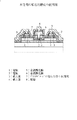
ここで、図1を参照して本発明における課題を解決するための手段を説明する。
図1参照
上述の課題を解決するために、本発明においては、半導体装置の電極1,2、または、電極1,2と半導体表面の双方のいずれかを、電極1,2の最上層3,4を構成する金と異なった金属、即ち、Ti,Co,Ta,Ni,Pd,Pr,Hf,Zrのいずれか一つの金属を構成元素とする金属酸化膜5,6によって被覆したことを特徴とする。
【0013】
このように、少なくとも電極1,2、特に、ショットキーバリアゲート電極やソース・ドレイン電極の表面を、電極1,2の最上層3,4を構成する金と異なった金属を構成元素とする金属酸化膜5,6、例えば、酸化Ti膜で被覆することによって、電極1,2の最上層3,4、特に、Au膜の表面に高抵抗な変質層が形成されるのが防止され、配線8との間のコンタクト不良を防止することが可能になる。
なお、電極1,2の最上層とは、電極1,2の形成を目的として堆積させた導電層の内の最上層3,4を意味するものであり、金属酸化物を形成するための金属が未反応のまま残存しても、本発明で言うところの「電極の最上層」ではない。
【0014】
また、半導体表面もこのような金属酸化膜5,6で被覆することによって、半導体層、例えば、キャリア供給層にプロセスダメージが導入されることが防止され、素子特性が劣化することがない。
【0015】
特に、金属酸化膜5,6を構成する金属としては、Ti,Co,Ta,Ni,Pd,Pr,Hf,Zrの酸化物の生成エネルギーの大きな金属を用いており、中でも、酸化Ti膜を用いた場合には、パッシベーション膜を構成するSiN膜と同じF系ガスを用いたドライエッチング或いはウェットエッチングによって同時にエッチング除去が可能になり、配線工程のプロセスが簡素化される。
【0016】
さらに、本発明は、電極1,2表面及び半導体表面が、プロセスダメージの発生を伴う保護膜7、即ち、プロセスダメージの発生を伴う成膜方法により形成されたSiN膜、SiON膜、または、SiO 2 膜で被覆されていることを特徴とする。
【0017】
このように、電極1,2表面及び半導体表面を金属酸化膜5,6で被覆しているので、緻密でパッシベーション膜として最適ではあるが、プロセスダメージの発生を伴う保護膜7、典型的にはプラズマCVD膜で被覆することが可能になる。
【0018】
また、本発明は、さらに、一部の電極2と半導体層との間にトンネル電流が流れる程度の厚さの金属酸化膜を介在させたことを特徴とする。
【0019】
金属酸化膜5,6の厚さがトンネル電流が流れる厚さであれば、一部の電極2と半導体層との間、典型的には、ゲート電極とキャリア供給層との間に、金属酸化膜を介在させても良く、それによって、熱的に安定なゲート電極を実現することができる。
【0020】
【発明の実施の形態】
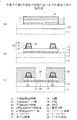
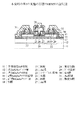
ここで、図2及び図3を参照して本発明の第1の実施の形態の製造工程を説明する。
図2(a)参照
まず、半絶縁性InP基板11上に、MOVPE法を用いて、厚さが、例えば、200nmのi型InAlAsバッファ層12、厚さが、例えば、25nmのi型InGaAsチャネル層13、厚さが、例えば、25nmで、n型不純物濃度が、例えば、2×1018cm-3のn型InAlAsキャリア供給層14、及び、厚さが、例えば、50nmで、n型不純物濃度が、例えば、1×1019cm-3のn+ 型InGaAsキャップ層15を順次成長させる。
なお、この場合のi型InGaAsチャネル層13及びn+ 型InGaAsキャップ層15の混晶比はIn0.53Ga0.47Asであり、また、i型InAlAsバッファ層12及びn型InAlAsキャリア供給層14の混晶比はIn0.52Al0.48Asである。
【0021】
次いで、レジストパターン16をマスクとして、H3 PO4 +H2 O2 +H2 Oからなるリン酸系のエッチャントを用いて、i型InAlAsバッファ層12が露出するまでエッチングして、素子分離溝17を形成する。
【0022】
図2(b)参照
次いで、レジストパターン16を除去したのち、新たにソース・ドレイン電極に対応する開口を有するレジストパターン(図示せず)を形成し、次いで、全面に、例えば、10nmのTi膜18、30nmのPt膜19、200nmのAu膜20、及び、2〜50nm、例えば、4nmのTi膜を蒸着法によって順次堆積させ、次いで、レジストパターンとともに不要なTi/Pt/Au/Ti膜をリフトオフすることによってノンアロイオーミック接触によりオーミック電極を形成する。
【0023】
次いで、酸素プラズマ雰囲気に晒すことによって、最上層のTi膜を酸化して酸化Ti膜21に変換して、Ti膜18/Pt膜19/Au膜20からなるとともに、表面が酸化Ti膜21で被覆されたソース・ドレイン電極22とする。
【0024】
この酸化工程において、Ti膜は堆積工程においてはTi膜18/Pt膜19/Au膜20構造の側面にも若干堆積するので、ソース・ドレイン電極22の側面も酸化Ti膜21で覆われることになる。
なお、下層のTi膜18については、側面からの酸化はあまり進行しないので問題はない。
【0025】
図2(c)参照
次いで、レジストパターンを除去したのち、新たにゲートリセス領域に対応する開口を有するレジストパターン23を設け、このレジストパターン23をマスクとして、クエン酸+H2 O2 +H2 Oからなるクエン酸系エッチャントを用いてn+ 型InGaAsキャップ層15を選択的に除去することによってゲートリセス領域24を形成する。
【0026】
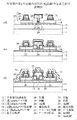
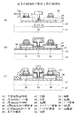
図3(d)参照
次いで、レジストパターン23を除去したのち、ゲート電極を形成するための開口パターンを有するリフトオフ用のレジストパターン(図示せず)を設けたのち、全面に、例えば、10nmのTi膜25、10nmのPt膜26、200nmのAu膜27、及び、2〜50nm、例えば、4nmのTi膜を蒸着法によって順次堆積させたのち、レジストパターンとともにリフトオフすることによって、不要なTi/Pt/Au/Ti膜を除去してショットキーバリア電極を形成する。
【0027】
次いで、再び、酸素プラズマ雰囲気に晒すことによって、最上層のTi膜を酸化して酸化Ti膜28に変換して、Ti膜25/Pt膜26/Au膜27からなるとともに、表面が酸化Ti膜28で被覆されたゲート電極29とする。
なお、Ti膜は堆積工程においてAu膜27の側面にも堆積するので、この酸化工程において、Au膜の側面も酸化Ti膜28で覆われることになる。
【0028】
図3(e)参照
次いで、プラズマCVD法によって、厚さが、例えば、100nmのSiN膜30を全面に堆積させてパッシベーション膜とする。
【0029】
図3(f)参照
次いで、ソース・ドレイン電極22及びゲート電極29に対応する開口部を有するレジストパターン(図示せず)を形成し、このレジストパターンをマスクとしてSF6 を用いたドライエッチングを施すことによって、SiN膜30及び酸化Ti膜21,28とを順次除去したのち、1μmのAu膜を順次堆積させたのち、Arイオンを用いたイオンミリングを施してAu配線31を形成することによってHEMTが完成する。
【0030】
以上、説明したように、本発明の第1の実施の形態においては、プラズマCVD法でSiN膜30を堆積する工程の前に、ゲート電極29及びソース・ドレイン電極22の表面を予め酸化Ti膜21,28で被覆・保護しているので、ゲート電極29及びソース・ドレイン電極22の最上層のAu膜20,27にプラズマ工程に伴うプラズマダメージが導入されることがなく、したがって、Au膜20,27の表面に高抵抗の変質層が形成されることがない。
【0031】
次に、図4及び図5を参照して、本発明の第2の実施の形態の製造工程を説明するが、酸化Ti膜の製造工程が異なる以外は、上記の第1の実施の形態と基本的に同一であるので、同じ工程に関しては説明は簡単にする。
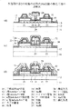
図4(a)参照
まず、上記の第1の実施の形態と全く同様に、半絶縁性InP基板11上に、i型InAlAsバッファ層12、i型InGaAsチャネル層13、n型InAlAsキャリア供給層14、及び、n+ 型InGaAsキャップ層15を順次成長させ、次いで、レジストパターン16をマスクとして、i型InAlAsバッファ層12が露出するまでエッチングして、素子分離溝17を形成する。
【0032】
図4(b)参照
次いで、レジストパターン16を除去したのち、新たにソース・ドレイン電極に対応する開口を有するレジストパターン(図示せず)を形成し、次いで、全面に、例えば、10nmのTi膜18、30nmのPt膜19、及び、200nmのAu膜20を蒸着法によって順次堆積させたのち、レジストパターンとともに不要なTi/Pt/Au膜をリフトオフすることによってノンアロイオーミック接触によりソース・ドレイン電極22を形成する。
【0033】
次いで、レジストパターンを除去したのち、新たにゲートリセス領域に対応するレジストパターン23を設け、このレジストパターン23をマスクとして、クエン酸系エッチャントを用いてn+ 型InGaAsキャップ層15を選択的に除去することによってゲートリセス領域24を形成する。
【0034】
図4(c)参照
次いで、レジストパターン23を除去したのち、全面に、厚さが、2〜10nm、例えば、4nmのTi膜を堆積させ、次いで、酸素プラズマ雰囲気に晒すことによって、Ti膜を酸化して酸化Ti膜32に変換して、ソース・ドレイン電極22及び半導体層の露出表面を酸化Ti膜32で被覆する。
【0035】
図5(d)参照
次いで、ゲート電極を形成するための開口パターンを有するリフトオフ用のレジストパターン(図示せず)を設けたのち、まず、SF6 ガスを用いたドライエッチングを施すことによって、ゲート形成予定部の酸化Ti膜32を選択的に除去する。
【0036】
次いで、全面に、例えば、10nmのTi膜25、10nmのPt膜26、200nmのAu膜27、及び、2〜50nm、例えば、4nmのTi膜を蒸着法によって順次堆積させたのち、レジストパターンとともにリフトオフすることによって、不要なTi/Pt/Au/Ti膜を除去してショットキーバリア電極を形成する。
【0037】
次いで、再び、酸素プラズマ雰囲気に晒すことによって、最上層のTi膜を酸化して酸化Ti膜28に変換して、Ti膜25/Pt膜26/Au膜27からなるとともに、表面が酸化Ti膜28で被覆されたゲート電極29とする。
【0038】
図5(e)参照
以降は、上記の第1の実施の形態と同様に、プラズマCVD法によって、厚さが、例えば、100nmのSiN膜30を全面に堆積させてパッシベーション膜とする。
【0039】
図5(f)参照
次いで、ソース・ドレイン電極22及びゲート電極29に接続するAu配線31を形成することによってHEMTが完成する。
【0040】
この様に、本発明の第2の実施の形態においては、ソース・ドレイン電極22及びゲート電極29以外に、n型InAlAsキャリア供給層14等の半導体層の露出表面を酸化Ti膜28,32で予め覆っているので、n型InAlAsキャリア供給層14等の半導体層にプラズマダメージが導入されることがなく、したがって、素子特性が劣化することがない。
【0041】
次に、図6を参照して、本発明の第3の実施の形態のHEMTを説明するが、ゲート電極の形成の前にゲート形成予定領域の酸化Ti膜を除去しない以外は上記の第2の実施の形態と基本的に同一であるので、説明は簡単にする。
図6参照
まず、上記の第2の実施の形態と全く同様に、図4(a)乃至図4(c)の工程を行うことによって、ソース・ドレイン電極22及び半導体の露出表面を酸化Ti膜32で被覆する。
【0042】
次いで、ゲート電極を形成するための開口パターンを有するリフトオフ用のレジストパターン(図示せず)を設けたのち、ゲート形成予定部の酸化Ti膜32を除去することなく、全面に、Ti膜25、Pt膜26、Au膜27、及び、Ti膜を蒸着法によって順次堆積させ、次いで、レジストパターンとともにリフトオフすることによって、不要なTi/Pt/Au/Ti膜を除去してショットキーバリア電極を形成する。
【0043】
以降は、再び、上記の第2の実施の形態と全く同様に、酸素プラズマ雰囲気に晒すことによって、Ti膜25/Pt膜26/Au膜27からなるとともに、表面が酸化Ti膜28で被覆されたゲート電極29とする。
【0044】
次いで、プラズマCVD法によって、厚さが、例えば、100nmのSiN膜30を全面に堆積させてパッシベーション膜としたのち、ソース・ドレイン電極22及びゲート電極29に接続するAu配線31を形成することによってHEMTが完成する。
【0045】
この様に、本発明の第3の実施の形態においては、ゲート電極29とn型InAlAsキャリア供給層14との間に酸化Ti膜32を介在させているので、熱的に特性の変動しない安定なゲート電極29を実現することができ、また、酸化Ti膜を除去する必要がないので、工程数を減らすことができる。
【0046】
なお、この場合の酸化Ti膜32の厚さは、2〜10nmのTi膜を酸化して形成したものであるので、トンネル電流が流れる程度の膜厚であり、したがって、ショットキーバリアゲート特性を保ったままとなる。
【0047】
以上、本発明の各実施の形態を説明してきたが、本発明は各実施の形態に記載した構成及び条件に限られるものではなく、各種の変更が可能である。
例えば、上記の各実施の形態においては、パッシベーション膜として、プラズマCVD法によって成膜したSiN膜を用いているが、SiN膜に限られるものではなく、プラズマCVD法によって成膜したSiON膜或いはSiO2 膜を用いても良いものである。
【0048】
また、上記の実施の形態においては、プラズマダメージの発生を伴うプラズマCVD法を例に説明しているが、プラズマCVD法に限られるものではなく、例えば、窒素雰囲気或いは酸素雰囲気中でSiターゲットをスパッタリングする成膜方法等の他のプロセスダメージの発生を伴う成膜方法によりパッシベーション膜を形成する場合にも適用されるものである。
【0049】
また、上記の各実施の形態においては、Ti膜の酸化を酸素プラズマ中に晒すことによって行っているが、高温工程を伴わない酸化方法であれば良く、Ti膜自体は薄いので、極端な場合には、自然酸化を利用しても良いものである。
【0050】
また、上記の各実施の形態においては、プラズマダメージからAu層を保護する保護膜として、SiN膜と同時にF系ガスによってドライエッチングが可能な酸化Ti膜を用いているが、酸化Ti膜に限られるものではなく、Co,Ta,Ni,Pd,Pr,Hf,Zr等の酸化物の生成エネルギーの大きな金属の酸化膜を用いても良いものである。
【0051】
また、上記の各実施の形態の説明においては、InP系HEMTとして説明しているが、InP系HEMTに限られるものではなく、GaAs系HEMTやMESFET等の他の電界効果型化合物半導体装置にも適用されるものである。
【0052】
さらには、ダイオード、光半導体素子等の他の化合物半導体装置にも適用されるものであり、要するに、電極として最上層がAu膜で構成される電極を設けるとともに、パッシベーション膜としてプロセスダメージの発生を伴う保護膜を設けている半導体装置に適用されるものである。
【0053】
【発明の効果】
本発明によれば、プロセスダメージの発生を伴うが緻密性の高い優れたパッシベーション膜を設ける前に、少なくとも電極の最上層を最上層を構成する金属と異なった金属の金属酸化膜で被覆・保護しているので、電極の表面に高抵抗な変質層が形成されることなく、配線との間のコンタクト不良が発生することがなく、ひいては、電界効果型化合物半導体装置の高性能化、信頼性の向上に寄与するところが大きい。
【図面の簡単な説明】
【図1】本発明の原理的構成の説明図である。
【図2】本発明の第1の実施の形態の途中までの製造工程の説明図である。
【図3】本発明の第1の実施の形態の図2以降の製造工程の説明図である。
【図4】本発明の第2の実施の形態の途中までの製造工程の説明図である。
【図5】本発明の第2の実施の形態の図4以降の製造工程の説明図である。
【図6】本発明の第3の実施の形態のHEMTの説明図である。
【図7】従来のHEMTの製造工程の説明図である。
【符号の説明】
1 電極
2 電極
3 最上層
4 最上層
5 金属酸化膜
6 金属酸化膜
7 プロセスダメージの発生を伴う保護膜
8 配線
11 半絶縁性InP基板
12 i型InAlAsバッファ層
13 i型InGaAsチャネル層
14 n型InAlAsキャリア供給層
15 n+ 型InGaAsキャップ層
16 レジストパターン
17 素子分離溝
18 Ti膜
19 Pt膜
20 Au膜
21 酸化Ti膜
22 ソース・ドレイン電極
23 レジストパターン
24 ゲートリセス領域
25 Ti膜
26 Pt膜
27 Au膜
28 酸化Ti膜
29 ゲート電極
30 SiN膜
31 Au配線
32 酸化Ti膜
41 半絶縁性InP基板
42 i型InAlAsバッファ層
43 i型InGaAsチャネル層
44 n型InAlAsキャリア供給層
45 n+ 型InGaAsキャップ層
46 素子分離溝
47 Ti膜
48 Pt膜
49 Au膜
50 ソース・ドレイン電極
51 ゲートリセス領域
52 Ti膜
53 Pt膜
54 Au膜
55 ゲート電極
56 SiN膜
57 Au配線[0001]
BACKGROUND OF THE INVENTION
The present invention relates to a semiconductor device, and more particularly, to an electrode covering structure for protecting an electrode of a field effect compound semiconductor device such as HEMT (High Electron Mobility Transistor) or MESFET (Metal-Semiconductor FET) from process damage. The present invention relates to a characteristic semiconductor device.
[0002]
[Prior art]
Conventionally, in Si devices such as silicon semiconductor integrated circuit devices, MISFETs (Metal-Insulator-Semiconductor FETs), that is, insulated gate FETs, have been used, but constitute high-frequency amplifier elements or ultra-high-speed integrated circuit devices. In an electronic device using a compound semiconductor such as GaAs, there is a problem of an interface state, and therefore MESFET, HEMT, and the like are used.
[0003]
Here, a manufacturing process of a conventional InP-based HEMT will be described with reference to FIG.
Each figure is a schematic cross-sectional view along the channel length direction.
7A. First, an i-type
[0004]
Next, after forming an
Next, after selectively removing the n + -type
[0005]
Next, referring to FIG. 7B, a
Note that the SiN
[0006]
Next, referring to FIG. 7C, an electrode lead-out portion is opened in a resist (not shown) by patterning, and then a lead-out opening is formed in the
[0007]
[Problems to be solved by the invention]
However, conventionally, a plasma CVD method is used in the process of forming the
[0008]
That is, since the Au
[0009]
In the plasma CVD process, plasma is generated by a silane (SiH 4 ) -based gas that is a raw material of SiN. Si ions in the plasma are irradiated on the surfaces of the source /
[0010]
Although it is possible to grow a film such as a SiN film by a low pressure chemical vapor deposition method (LPCVD method) which does not cause process damage, there is a problem that the denseness required for a passivation film cannot be obtained. .
[0011]
Accordingly, an object of the present invention is to provide an electrode structure having excellent process damage resistance.
[0012]
[Means for Solving the Problems]
Here, means for solving the problems in the present invention will be described with reference to FIG.
In order to solve the above-described problem, in the present invention, either of the
[0013]
As described above, at least the
The uppermost layer of the
[0014]
In addition, by covering the semiconductor surface with such
[0015]
In particular, as the metal constituting the
[0016]
Further, the present invention provides a
[0017]
As described above, since the surfaces of the
[0018]
The present invention is further characterized in that a metal oxide film having a thickness sufficient to allow a tunnel current to flow is interposed between some of the
[0019]
If the thickness of the
[0020]
DETAILED DESCRIPTION OF THE INVENTION
Here, the manufacturing process of the first embodiment of the present invention will be described with reference to FIGS.
2A. First, an i-type
In this case, the mixed crystal ratio of the i-type
[0021]
Next, using the resist
[0022]
2B, after removing the resist
[0023]
Next, by exposing to an oxygen plasma atmosphere, the uppermost Ti film is oxidized and converted to the
[0024]
In this oxidation step, the Ti film is slightly deposited also on the side surfaces of the
The
[0025]
Next, after removing the resist pattern, a resist
[0026]
Next, after removing the resist
[0027]
Next, by exposing again to an oxygen plasma atmosphere, the uppermost Ti film is oxidized and converted to the
Since the Ti film is also deposited on the side surface of the
[0028]
Next, referring to FIG. 3E, a
[0029]
Next, referring to FIG. 3F, a resist pattern (not shown) having openings corresponding to the source /
[0030]
As described above, in the first embodiment of the present invention, before the step of depositing the
[0031]
Next, the manufacturing process of the second embodiment of the present invention will be described with reference to FIG. 4 and FIG. 5, except that the manufacturing process of the Ti oxide film is different from that of the first embodiment. Since they are basically the same, the description of the same process is simplified.
4A. First, in the same manner as in the first embodiment, an i-type
[0032]
4B, after removing the resist
[0033]
Next, after removing the resist pattern, a resist
[0034]
4C. Next, after removing the resist
[0035]
Next, referring to FIG. 5D, after providing a lift-off resist pattern (not shown) having an opening pattern for forming a gate electrode, first, dry etching using SF 6 gas is performed. The
[0036]
Next, for example, a 10
[0037]
Next, by exposing again to an oxygen plasma atmosphere, the uppermost Ti film is oxidized and converted to the
[0038]
After FIG. 5E, the
[0039]
Next, the HEMT is completed by forming Au wirings 31 connected to the source /
[0040]
Thus, in the second embodiment of the present invention, the exposed surface of the semiconductor layer such as the n-type InAlAs
[0041]
Next, a HEMT according to a third embodiment of the present invention will be described with reference to FIG. 6, except that the Ti oxide film in the gate formation scheduled region is not removed before the gate electrode is formed. Since this is basically the same as the embodiment, the description will be simplified.
6 First, in the same manner as in the second embodiment, by performing the steps of FIGS. 4A to 4C, the source /
[0042]
Next, after providing a lift-off resist pattern (not shown) having an opening pattern for forming a gate electrode, the
[0043]
Thereafter, the film is again formed of the
[0044]
Next, a
[0045]
As described above, in the third embodiment of the present invention, since the
[0046]
In this case, since the thickness of the
[0047]
Although the embodiments of the present invention have been described above, the present invention is not limited to the configurations and conditions described in the embodiments, and various modifications can be made.
For example, in each of the above embodiments, a SiN film formed by plasma CVD is used as the passivation film. However, the present invention is not limited to the SiN film, and the SiON film or SiON film formed by plasma CVD is used. Two films may be used.
[0048]
In the above embodiment, the plasma CVD method accompanied by the occurrence of plasma damage is described as an example. However, the present invention is not limited to the plasma CVD method. For example, the Si target is used in a nitrogen atmosphere or an oxygen atmosphere. The present invention is also applied to the case where a passivation film is formed by a film forming method that involves generation of other process damage such as a film forming method for sputtering.
[0049]
In each of the above embodiments, the oxidation of the Ti film is performed by exposing it to oxygen plasma. However, an oxidation method that does not involve a high-temperature process may be used, and the Ti film itself is thin. For this, natural oxidation may be used.
[0050]
In each of the above embodiments, as the protective film for protecting the Au layer from plasma damage, a TiN film that can be dry-etched by F-based gas simultaneously with the SiN film is used. Instead, a metal oxide film having a large generation energy of oxides such as Co, Ta, Ni, Pd, Pr, Hf, and Zr may be used.
[0051]
In the description of each of the above embodiments, the InP-based HEMT is described. However, the present invention is not limited to the InP-based HEMT, and other field effect type compound semiconductor devices such as a GaAs-based HEMT and MESFET are also used. Applicable.
[0052]
Furthermore, it is also applied to other compound semiconductor devices such as diodes, optical semiconductor elements, etc. In short, an electrode whose uppermost layer is made of an Au film is provided as an electrode, and process damage is generated as a passivation film. The present invention is applied to a semiconductor device provided with the accompanying protective film.
[0053]
【The invention's effect】
According to the present invention, at least the uppermost layer of the electrode is covered and protected with a metal oxide film of a metal different from the metal constituting the uppermost layer before providing an excellent passivation film that is accompanied by the occurrence of process damage but is highly dense. As a result, a high-resistance deteriorated layer is not formed on the surface of the electrode, no contact failure with the wiring occurs, and as a result, high performance and reliability of the field effect compound semiconductor device The place that contributes to the improvement of
[Brief description of the drawings]
FIG. 1 is an explanatory diagram of a basic configuration of the present invention.
FIG. 2 is an explanatory diagram of the manufacturing process up to the middle of the first embodiment of the present invention.
FIG. 3 is an explanatory diagram of the manufacturing process from FIG. 2 onward according to the first embodiment of the present invention.
FIG. 4 is an explanatory diagram of the manufacturing process up to the middle of the second embodiment of the present invention.
FIG. 5 is an explanatory diagram of the manufacturing process after FIG. 4 according to the second embodiment of the present invention.
FIG. 6 is an explanatory diagram of a HEMT according to a third embodiment of this invention.
FIG. 7 is an explanatory diagram of a manufacturing process of a conventional HEMT.
[Explanation of symbols]
DESCRIPTION OF
Claims (3)
Priority Applications (1)
| Application Number | Priority Date | Filing Date | Title |
|---|---|---|---|
| JP2000192112A JP4606552B2 (en) | 2000-06-27 | 2000-06-27 | Semiconductor device |
Applications Claiming Priority (1)
| Application Number | Priority Date | Filing Date | Title |
|---|---|---|---|
| JP2000192112A JP4606552B2 (en) | 2000-06-27 | 2000-06-27 | Semiconductor device |
Publications (2)
| Publication Number | Publication Date |
|---|---|
| JP2002016086A JP2002016086A (en) | 2002-01-18 |
| JP4606552B2 true JP4606552B2 (en) | 2011-01-05 |
Family
ID=18691287
Family Applications (1)
| Application Number | Title | Priority Date | Filing Date |
|---|---|---|---|
| JP2000192112A Expired - Lifetime JP4606552B2 (en) | 2000-06-27 | 2000-06-27 | Semiconductor device |
Country Status (1)
| Country | Link |
|---|---|
| JP (1) | JP4606552B2 (en) |
Families Citing this family (3)
| Publication number | Priority date | Publication date | Assignee | Title |
|---|---|---|---|---|
| JP2012175089A (en) | 2011-02-24 | 2012-09-10 | Fujitsu Ltd | Semiconductor device and method of manufacturing semiconductor device |
| JP2016103646A (en) * | 2015-12-14 | 2016-06-02 | 富士通株式会社 | Semiconductor device and method of manufacturing semiconductor device |
| CN119213571A (en) * | 2022-05-30 | 2024-12-27 | 三菱电机株式会社 | Semiconductor device and method for manufacturing semiconductor device |
Family Cites Families (8)
| Publication number | Priority date | Publication date | Assignee | Title |
|---|---|---|---|---|
| JPS50114170A (en) * | 1974-02-15 | 1975-09-06 | ||
| JPS5795626A (en) * | 1980-12-05 | 1982-06-14 | Toshiba Corp | Manufacture of semiconductor device |
| JPH0284725A (en) * | 1988-01-20 | 1990-03-26 | Nippon Mining Co Ltd | Semiconductor device and manufacture thereof |
| JP2932304B2 (en) * | 1990-07-11 | 1999-08-09 | サンケン電気株式会社 | Method of manufacturing semiconductor device having Schottky barrier |
| JP3058040B2 (en) * | 1995-01-18 | 2000-07-04 | 株式会社村田製作所 | Semiconductor device |
| JPH0936393A (en) * | 1995-07-25 | 1997-02-07 | Denso Corp | Method of manufacturing semiconductor device having Schottky junction |
| JP3251554B2 (en) * | 1998-12-04 | 2002-01-28 | キヤノン販売株式会社 | Film forming method and semiconductor device manufacturing method |
| JP4751498B2 (en) * | 2000-03-30 | 2011-08-17 | 富士通株式会社 | Semiconductor three-terminal device |
-
2000
- 2000-06-27 JP JP2000192112A patent/JP4606552B2/en not_active Expired - Lifetime
Also Published As
| Publication number | Publication date |
|---|---|
| JP2002016086A (en) | 2002-01-18 |
Similar Documents
| Publication | Publication Date | Title |
|---|---|---|
| JP4751498B2 (en) | Semiconductor three-terminal device | |
| US4679311A (en) | Method of fabricating self-aligned field-effect transistor having t-shaped gate electrode, sub-micron gate length and variable drain to gate spacing | |
| JP2005191022A (en) | Field effect transistor and manufacturing method thereof | |
| US6642099B2 (en) | Method of manufacturing compound semiconductor device | |
| JPH0332218B2 (en) | ||
| US5362658A (en) | Method for producing semiconductor device | |
| JP4606552B2 (en) | Semiconductor device | |
| JP3470065B2 (en) | Semiconductor integrated circuit and manufacturing method thereof | |
| JP3119248B2 (en) | Field effect transistor and method of manufacturing the same | |
| JP3347947B2 (en) | Method for manufacturing semiconductor device | |
| JP3509682B2 (en) | Heterojunction bipolar transistor, method of manufacturing the same, and communication device | |
| JP2001210658A (en) | Method for manufacturing field effect transistor | |
| JP3127863B2 (en) | Semiconductor device and manufacturing method thereof | |
| JP2002100640A (en) | Field effect type compound semiconductor device | |
| JP3099874B2 (en) | Semiconductor device and manufacturing method thereof | |
| JP4546051B2 (en) | Manufacturing method of semiconductor device | |
| JP2008010467A (en) | Semiconductor device and manufacturing method thereof | |
| JP3434623B2 (en) | Field effect transistor | |
| JP3343194B2 (en) | Heterojunction field effect transistor and method of manufacturing the same | |
| JP2001044217A (en) | Compound semiconductor device and method of manufacturing the same | |
| JP3520625B2 (en) | Method for manufacturing semiconductor device | |
| JPH10261658A (en) | Method for manufacturing semiconductor device | |
| JP3715461B2 (en) | Semiconductor device and manufacturing method thereof | |
| JP2001267554A (en) | Field effect transistor and method of manufacturing the same | |
| JP3710613B2 (en) | Semiconductor device |
Legal Events
| Date | Code | Title | Description |
|---|---|---|---|
| A621 | Written request for application examination |
Free format text: JAPANESE INTERMEDIATE CODE: A621 Effective date: 20070424 |
|
| A977 | Report on retrieval |
Free format text: JAPANESE INTERMEDIATE CODE: A971007 Effective date: 20100624 |
|
| A131 | Notification of reasons for refusal |
Free format text: JAPANESE INTERMEDIATE CODE: A131 Effective date: 20100629 |
|
| A521 | Request for written amendment filed |
Free format text: JAPANESE INTERMEDIATE CODE: A523 Effective date: 20100827 |
|
| TRDD | Decision of grant or rejection written | ||
| A01 | Written decision to grant a patent or to grant a registration (utility model) |
Free format text: JAPANESE INTERMEDIATE CODE: A01 Effective date: 20101005 |
|
| A01 | Written decision to grant a patent or to grant a registration (utility model) |
Free format text: JAPANESE INTERMEDIATE CODE: A01 |
|
| A61 | First payment of annual fees (during grant procedure) |
Free format text: JAPANESE INTERMEDIATE CODE: A61 Effective date: 20101006 |
|
| R150 | Certificate of patent or registration of utility model |
Ref document number: 4606552 Country of ref document: JP Free format text: JAPANESE INTERMEDIATE CODE: R150 Free format text: JAPANESE INTERMEDIATE CODE: R150 |
|
| FPAY | Renewal fee payment (event date is renewal date of database) |
Free format text: PAYMENT UNTIL: 20131015 Year of fee payment: 3 |
|
| EXPY | Cancellation because of completion of term |