JP4585661B2 - Electro-optical array, charged particle beam exposure apparatus, and device manufacturing method - Google Patents
Electro-optical array, charged particle beam exposure apparatus, and device manufacturing method Download PDFInfo
- Publication number
- JP4585661B2 JP4585661B2 JP2000233145A JP2000233145A JP4585661B2 JP 4585661 B2 JP4585661 B2 JP 4585661B2 JP 2000233145 A JP2000233145 A JP 2000233145A JP 2000233145 A JP2000233145 A JP 2000233145A JP 4585661 B2 JP4585661 B2 JP 4585661B2
- Authority
- JP
- Japan
- Prior art keywords
- electrode
- optical system
- charged particle
- system array
- shield
- Prior art date
- Legal status (The legal status is an assumption and is not a legal conclusion. Google has not performed a legal analysis and makes no representation as to the accuracy of the status listed.)
- Expired - Fee Related
Links
Images


Classifications
-
- H—ELECTRICITY
- H01—ELECTRIC ELEMENTS
- H01J—ELECTRIC DISCHARGE TUBES OR DISCHARGE LAMPS
- H01J37/00—Discharge tubes with provision for introducing objects or material to be exposed to the discharge, e.g. for the purpose of examination or processing thereof
- H01J37/02—Details
- H01J37/04—Arrangements of electrodes and associated parts for generating or controlling the discharge, e.g. electron-optical arrangement, ion-optical arrangement
- H01J37/10—Lenses
- H01J37/12—Lenses electrostatic
-
- G—PHYSICS
- G01—MEASURING; TESTING
- G01N—INVESTIGATING OR ANALYSING MATERIALS BY DETERMINING THEIR CHEMICAL OR PHYSICAL PROPERTIES
- G01N23/00—Investigating or analysing materials by the use of wave or particle radiation, e.g. X-rays or neutrons, not covered by groups G01N3/00 – G01N17/00, G01N21/00 or G01N22/00
-
- H—ELECTRICITY
- H01—ELECTRIC ELEMENTS
- H01J—ELECTRIC DISCHARGE TUBES OR DISCHARGE LAMPS
- H01J37/00—Discharge tubes with provision for introducing objects or material to be exposed to the discharge, e.g. for the purpose of examination or processing thereof
- H01J37/30—Electron-beam or ion-beam tubes for localised treatment of objects
- H01J37/3002—Details
- H01J37/3007—Electron or ion-optical systems
-
- H—ELECTRICITY
- H01—ELECTRIC ELEMENTS
- H01J—ELECTRIC DISCHARGE TUBES OR DISCHARGE LAMPS
- H01J9/00—Apparatus or processes specially adapted for the manufacture, installation, removal, maintenance of electric discharge tubes, discharge lamps, or parts thereof; Recovery of material from discharge tubes or lamps
- H01J9/02—Manufacture of electrodes or electrode systems
- H01J9/14—Manufacture of electrodes or electrode systems of non-emitting electrodes
-
- H—ELECTRICITY
- H01—ELECTRIC ELEMENTS
- H01J—ELECTRIC DISCHARGE TUBES OR DISCHARGE LAMPS
- H01J9/00—Apparatus or processes specially adapted for the manufacture, installation, removal, maintenance of electric discharge tubes, discharge lamps, or parts thereof; Recovery of material from discharge tubes or lamps
- H01J9/02—Manufacture of electrodes or electrode systems
- H01J9/18—Assembling together the component parts of electrode systems
-
- H—ELECTRICITY
- H01—ELECTRIC ELEMENTS
- H01J—ELECTRIC DISCHARGE TUBES OR DISCHARGE LAMPS
- H01J2237/00—Discharge tubes exposing object to beam, e.g. for analysis treatment, etching, imaging
- H01J2237/10—Lenses
- H01J2237/12—Lenses electrostatic
- H01J2237/1205—Microlenses
-
- H—ELECTRICITY
- H01—ELECTRIC ELEMENTS
- H01J—ELECTRIC DISCHARGE TUBES OR DISCHARGE LAMPS
- H01J2237/00—Discharge tubes exposing object to beam, e.g. for analysis treatment, etching, imaging
- H01J2237/15—Means for deflecting or directing discharge
- H01J2237/151—Electrostatic means
-
- H—ELECTRICITY
- H01—ELECTRIC ELEMENTS
- H01J—ELECTRIC DISCHARGE TUBES OR DISCHARGE LAMPS
- H01J2237/00—Discharge tubes exposing object to beam, e.g. for analysis treatment, etching, imaging
- H01J2237/153—Correcting image defects, e.g. stigmators
- H01J2237/1534—Aberrations
-
- H—ELECTRICITY
- H01—ELECTRIC ELEMENTS
- H01J—ELECTRIC DISCHARGE TUBES OR DISCHARGE LAMPS
- H01J2237/00—Discharge tubes exposing object to beam, e.g. for analysis treatment, etching, imaging
- H01J2237/30—Electron or ion beam tubes for processing objects
- H01J2237/317—Processing objects on a microscale
- H01J2237/3175—Lithography
- H01J2237/31774—Multi-beam
Description
【0001】
【発明の属する技術分野】
本発明は、複数の荷電粒子光学系をアレイにした荷電粒子光学系アレイに関するものである。
【0002】
【従来の技術】
半導体デバイスの生産において、電子ビーム露光技術は0.1μm以下の微細パターン露光を可能とするリソグラフィの有力候補として脚光を浴びており、いくつかの方式がある。例えば、いわゆる一筆書きでパターンを描画する可変矩形ビーム方式がある。しかしこれはスループットが低く量産用露光機としては課題が多い。スループットの向上を図るものとして、ステンシルマスクに形成したパターンを縮小転写する図形一括露光方式が提案されている。この方式は、繰り返しの多い単純パターンには有利であるが、ロジック配線層等のランダムパターンではスループットの点で課題が多く、実用化に際して生産性向上の妨げが大きい。
【0003】
これに対して、マスクを用いずに複数本の電子ビームで同時にパターンを描画するマルチビームシステムの提案がなされており、物理的なマスク作製や交換をなくし、実用化に向けて多くの利点を備えている。電子ビームをマルチ化する上で重要となるのが、これに使用する電子レンズのアレイ数である。電子ビーム露光装置の内部に配置できる電子レンズのアレイ数によりビーム数が決まり、スループットを決定する大きな要因となる。このため電子レンズの性能を高めながら且つ如何に小型化できるかが、マルチビーム型露光装置の性能向上のカギのひとつとなる。
【0004】
電子レンズには電磁型と静電型があり、静電型は磁界型に比べて、コイルコア等を設ける必要がなく構成が容易であり小型化に有利となる。ここで静電型の電子レンズ(静電レンズ)の小型化に関する主な従来技術を以下に示す。
【0005】
A.D. Feinerman等(J. Vac. Sci. Technol. A 10(4), p611, 1992)は、ファイバとSiの結晶異方性エッチングにより作製したV溝を用いたマイクロメカニクス技術により、静電単一レンズである3枚の電極からなる3次元構造体を形成することを開示する。Siにはメンブレン枠とメンブレンと該メンブレンに電子ビームが通過する開口を設ける。また、K.Y. Lee等(J. Vac. Sci. Technol. B 12(6), p3425, 1994)は、陽極接合法を利用してSiとパイレックスガラスが複数積層に接合された構造体を開示するもので、高精度にアライメントされたマイクロカラム用電子レンズを作製する。また、Sasaki(J. Vac. Sci. Technol. 19, 963 (1981))はレンズ開口配列を有する3枚電極でアインツェルレンズ配列にした構成を開示する。また、Chang等(J. Vac. Sci. Technol. B10,2743 (1992))は、アインツェルレンズを有するマイクロカラムを複数配列した構成を提案している。
【0006】
【発明が解決しようとする課題】
しかしながら、上記従来例において多数の開口電極をアレイ状に配列し、各電子ビームに異なるレンズ作用を与えようとすると、周囲の静電レンズ電界の影響で軌道や収差が変化し、各電子ビームを独立に操作することが困難になる、所謂クロストーク問題を生じる可能性がある。
【0007】
このクロストーク問題を図10を用いて具体的に説明する。上電極1、中間電極2及び下電極3の3枚電極でアインツェルレンズを構成している。上電極1及び下電極3は厚さ10μmであり、径 80μmの開口が 200μmピッチで配されている。中間電極2は厚さ50μmであり、内径80μmの円筒形状をしており、これが200μmピッチで配されている。上電極1と中間電極2、中間電極2と下電極3の距離は共に100μmである。上電極1及び下電極3に電位0[V]を、中央列Bとその上列Aの中間電極2には−1000[V]を、下列Cの中間電極2には−950[V]を印加する。すなわち隣接電極間電位差は50[V]である。この場合、上電極1の左方より、ビーム径40μm、エネルギ 50 keVの電子ビームを中央の開口に入射すると、電子ビームの下方シフト角Δθ十数μrad以上となる。電子光学系の設計にも依るが、典型的な許容値として、シフト角Δθを1μrad以下に設定することが可能であるが、この電極構成ではシフト角はこの許容範囲を越えるため、周囲のレンズ電界の影響を受けて、いわゆるクロストークが発生する。これを解決することが大きな課題である。
【0008】
本発明の目的のひとつは、クロストークを軽減した荷電粒子光学系アレイを提供することである。
【0009】
【課題を解決するための手段】
本発明の第一の荷電粒子光学系アレイは、それぞれに複数の開口が形成されていて且つ互いに積層された第1電極および第2電極と、前記第1電極と前記第2電極との間において前記複数の開口のそれぞれに対応して設けられたシールド電極と、を有することを特徴とする荷電粒子光学系アレイである。
【0010】
本発明の第二の荷電粒子光学系アレイは、それぞれに複数の開口が形成されていて且つ互いに積層された上電極、中間電極および下電極と、前記上電極と前記中間電極との間ならびに前記中間電極と前記下電極との間のそれぞれにおいて前記複数の開口のそれぞれに対応して設けられたシールド電極と、を有することを特徴とする荷電粒子光学系アレイである。
【0011】
本発明の荷電粒子線露光装置は、複数の荷電粒子線でウエハを露光する露光装置であって、前記複数の荷電粒子線を形成する荷電粒子光学系を有し、前記荷電粒子光学系は、請求項1〜14のいずれか一項に記載の荷電粒子光学系アレイを含むことを特徴とする露光装置である。
【0012】
本発明のデバイス製造方法は、上述の露光装置を用いて基板を露光する工程と、前記工程で露光された基板を現像する工程と、を含むことを特徴とするデバイス製造方法である。
【0013】
【発明の実施の形態】
<電子光学系アレイ>
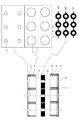
本発明の実施の形態にかかる電子光学系アレイを図面を用いて説明する。図1は電子光学系アレイの分解図である。図中、大きくは、それぞれに複数の開口が形成された上電極1、上シールド電極4、中間電極2、下シールド電極5、下電極3が順に積層された構造を有する。上電極1は導電性材料(Cu)の電極層で形成された厚さ10μmの薄膜構造であって、直径80μmの円形の開口8が200μmピッチで規則的に複数配されている。また下電極5も同様の構成を有し、上電極の開口と同一位置に複数の開口14が形成されている。中間電極2は、内側に開口10が形成された円筒形状(厚さ50μm、内径80μm、外径170μm)の導電性材料(Cu)の円筒電極素子(孔開き電極素子)11を複数有すると共に、各円筒電極素子11は、列ごと(A列、B列、C列)にグループ化され、各列に含まれる円筒電極素子11は幅4μmの帯状のCu配線12で電気的に結線された構造を有する。上シールド電極4ならびに下シールド電極5は、いずれも厚さ88μmの導電性(Cu)の板に内径160 μmの円形の開口9、13が、200μmピッチで規則的に形成された構造物である。上電極1、上シールド電極4、中間電極2、シールド電極5、下電極3、中間電極2にそれぞれ規則的に配された開口は、各開口の中心が光軸方向から見たときに一致するように配されている。上電極1と上シールド電極4とは絶縁層6を介して接合され、下電極3と下シールド電極5とは絶縁層7を介して接合されている。これら絶縁層6、絶縁層7はいずれも厚さ1μmであるため、上電極1と上シールド電極4ならびに下電極3と下シールド電極5との距離は共に1μmとなっている。また上電極1と中間電極2、下電極3と中間電極2との距離はいずれも100μmである。上シールド電極4及び下シールド電極5における各電極の開口サイズ(内径)を、中間電極2、上電極1及び下電極3の各電極の開口サイズ(内径)よりも大きくしているので、シールド電極を挿入することによるレンズ作用への影響が小さくなっている。
【0014】
上記構成の電子光学系アレイにおいて、先の図10と同様に、上電極1、上シールド電極4、下シールド電極5及び下電極3に0[V]の電位を与え、中間電極2のB列(中央列)とA列には−1000[V]の電位を、中間電極2のC列には−950[V]を印加して、B列とC列との隣接電位差が50[V]であるとする。このとき、ビームシフト角Δθは0.8mμ rad、ビーム径(最小錯乱円)は0.6μmと許容範囲内に収まり、クロストークの発生が実用的には問題にない程度に抑えられる。なお、変形例として、上電極1と下電極3にのみ0[V]の電位を与え、その間の上シールド電極4と下シールド電極5に他とは異なる共通電位Vs[V](たとえば−500V)を与えるようにしてもよい。本例によれば、それぞれに複数の開口が形成され、積層された上電極、中間電極および下電極を備えた電子光学系アレイにおいて、上電極と中間電極の間ならびに中間電極と下電極の間で、前記複数の開口のそれぞれに対応してシールド電極を設けることで、隣接レンズ電界の影響を抑える事が可能となり、良好にクロストークを抑えることができる。
【0015】
次に上記構造の電子光学系アレイの作製方法を説明する。ここでは説明を簡単にするために1つの開口部のみをクローズアップする。
【0016】
まず上電極1と上シールド電極4の作製方法について説明する。なお、下電極3と下シールド電極5もこれを同様の方法で作成する。
【0017】
最初に基板として結晶方位が<100>のシリコンウェーハを用意し、化学気層蒸着法にて膜厚300nmの窒化珪素を成膜する(図2(a))。レジストプロセスとエッチングプロセスを経て、後に電子線の光路になる部分と電極間の位置合わせを行う部分の窒化珪素膜を除去する。次いで開口部のシリコン基板をテトラメチルアンモニウムヒドロキシド水溶液で深さ1〜2μm程度異方性エッチングを行い、基板の少なくとも一つの面にV字上のV溝を形成する。次にこのV溝が形成された面に上電極としてクロム/金をそれぞれ50nm/1μmの膜厚で連続蒸着し、レジストパターニング後、金/クロムをエッチングして電子ビーム用開口を形成する(図2(b))。次にSiO2膜を1μmスパッター蒸着,パターニングする。更に、上シールド電極を作製する為のメッキ用の電極膜としてクロム/金をそれぞれ5nm/50nmの膜厚で連続蒸着、パターニングする(図2(c))。この後、電極上にメッキの鋳型となるレジストパターンを形成する。レジストにはエポキシ化ビスフェノールAオリゴマーを主成分とするSU−8(MicroChem.co)を用い、膜厚100μmに成膜する。露光は高圧水銀ランプを用いた密着型の露光装置を用いる。また、露光後ホットプレート上85℃で30分間、露光後ベーク(PEB)を行なう。基板を室温まで徐冷した後プロピレングリコールモノメチルエーテルアセテートで5分間現像し、メッキ用の鋳型パターンを形成する。次に電気めっきにより、レジストの開口部に金属パターンを埋め込む。電気めっきで膜厚89μmの金パターンをレジストパターン間隙に埋め込む(図2(d))。SU−8レジストを剥離し、IPAで洗浄、乾燥を行い、金パターンを得る(図2(e))。メッキ面をポリイミドを用いて保護し(不図示)、他方の面を22%のテトラメチルアンモニウムヒドロキシド水溶液を用い、90℃でシリコン基板のバックエッチングを行なう。エッチングは、シリコンがエッチング除去され、窒化珪素膜が露出するまで行なう。基板は水洗、乾燥を行い、ドライエッチング装置内でテトラフルオロメタンを用いて、シリコンのエッチング後に露出した窒化珪素膜をエッチング除去する。最後に、他方の面の保護をしたポリイミド膜をアッシングにより除去する(図2(f))。
【0018】
中間電極2の作製方法は以下の通りである。基板としてシリコンウェーハを用意し、スパッター法によりSiO2を50 nmの厚さに成膜する。次に中間電極を作製する為のメッキ用の電極膜として金を50nmの膜厚で蒸着、パターニングする(図3(a))。この後、メッキの鋳型となるレジストパターンを形成する。レジストは、エポキシ化ビスフェノールAオリゴマーオリゴマーを主成分とするSU−8(MicroChem.co)を用い、膜厚80μmに成膜する。露光は高圧水銀ランプを用いた密着型の露光装置を用いて行なう。また、露光後ホットプレート上85℃で30分間、露光後ベーク(PEB)を行う。基板を室温まで徐冷した後プロピレングリコールモノメチルエーテルアセテートで5分間現像し、メッキ用の鋳型パターンを形成する(図3(b))。次に電気めっきにより、レジストの開口部に金属パターンを埋め込む。電気めっきを行い膜厚50μmの金パターンをレジストパターン間隙に埋め込む(図3(c))。最後に、N−メチルピロリドン(NMP)中でSU−8レジストを剥離し、IPAで洗浄、乾燥を行い、金パターンを得る(図3(d))。
【0019】
下電極と中間電極の接合方法を図4を用いて説明する。前記図2の手順で作製した下電極及び下シールド電極(f)を用意する。これにSiO2をスパッタ法により10μm成膜しパターニングした後、金50nmを蒸着パターニングする(図4(a))。そして図3(d)で作製した中間電極を上下逆にしてこれと金・金接合で圧着する(図4(b)(c))。その後、治具を使って中間電極側のシリコンウエハのみをウェットエッチングし、SiO250nmと金50nmをドライエッチングで除去して、接合された下電極/中間電極を得る(図4(d))。
【0020】
図5は最終的な組立てを説明する図である。上記図4(d)で作製した接合された下電極・下シールド電極・中間電極と、上記図2(f)で作製した上電極・上シールド電極とを対面させ、両側の基板上に形成された位置合わせ用のV溝に合わせてファイバ20を設置し、両者に圧力を作用させることによって、接合面に平行な方向と垂直な方向に位置決めが達成される。位置決めされた部材同士の固定には接着剤を用いる。こうして組立精度に優れた電子光学素子アレイが完成する。
【0021】
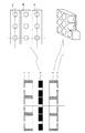
次に、上記説明した電子光学系アレイの変形例をいくつか説明する。図6は中間電極を複数持った構成例を示す分解図である。中間電極が1枚であった先の図1の例に対し、光軸に沿って、中間電極2A、中間電極2Bの2つを有し、それらの間には中間シールド電極15を挟んでいる。
【0022】
図7は、シールド電極を別体にせず1つの電極として一体形成した例である。すなわち上電極1と上シールド電極4、ならびに下電極3と下シールド電極5とをそれぞれ金属材料の一体構造とし、両者の間には絶縁層を設けないようにしている。このため製造プロセスをより簡略化することができる。
【0023】
図8はさらに別の構造例である。中間電極の複数の円筒電極素子同士の隙間に中間シールド電極が配されている図7の中間電極の周囲に中間電極シールド16が配されている。隣接電界の影響がより小さくなり、クロストーク防止効果がより向上する。
【0024】
図9はさらに別の構造例である。中間電極が列ごとにアレイ化された複数の矩形電極素子2A、2B,2Cを有し、各電極素子ごとに異なる電位を印加できる。電極素子を矩形形状とすることで構造体としての剛性が向上するのに加えてプロセス精度も向上する。
【0025】
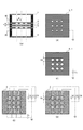
図11は更に別の形態の電子レンズアレイを示す図である。図11(A)はレンズアレイの断面図であり、複数の開口電極が形成された上電極1、中間電極2、及び下電極3を有する。中間電極2の開口電極のそれぞれを囲むように、共通の電位に設定される上シールド電極4,下シールド電極5を設けている。各電極は絶縁材からなるスペーサ20を介して積み重ねて一体化されている。図11(B)は上電極1又は下電極3の構造を示し、複数の開口電極の全てO[V]の電位に接地されている。図11(C)は上シールド電極4及び下シールド電極5の構造を示し、全ての開口電極に共通の電位Vs(例えば−500V)が印加される。図11(D)は中間電極2の構造を示し、複数の開口電極の列毎に互いに異なる電位V1、V2、V3(例えば、V1=−900V 、V2=−950V 、V3=−1000V)が印加される。これにより異なる列の中間電極を有するアインツエルレンズは互いに異なるレンズ作用を有し、中間電極はアインツエルレンズのレンズ作用を設定する設定用電極と見なすことができる。なお、本実施形態に限らず上記説明した他の形態においても、このような電位の与え方をしてもよい。
【0026】
クロストーク低減を効果的にするために、図11(A)に示すように中間電極2と上シールド電極4,下シールド電極5のそれぞれの間隔sは、中間電極2に形成される開口電極の配列間隔(ピッチ)pに比べ小さくしている。更に、シールド電極を挿入することによるレンズ作用への影響を小さくするために、シールド電極4.5における各電極の開口サイズDs(内径)(図11C)参照)は、中間電極2における各電極の開口サイズDc(内径)(図11(D)参照)に比べて大きくしている。また、上電極1及び下電極3の各電極の開口サイズよりもシールド電極4,5の各電極の開口サイズを大きくしている。
【0027】
なお、図11(E)に示すような中間電極の構造としてもよい。同図において、中間電極2は、互いに異なる電位(V1、V2、V3)に設定される電極列のそれぞれの間に、直線上に形成した中間シールド電極を挿入している。そして各中間シールド電極には、上記シールド電極4,5と同一の共通電位Vsが印加される。中間電極の中で、各電極列の間をシールドすることでより効果的にクロストークを防止している。
【0028】
図12はさらなる変形例を示す。Y方向に電極列が形成された中間電極24を含むユニットLA1と、これと直交するX方向に電極列が形成されている中間電極27と含むユニットLA2とを一体化したものである。そしてユニットLA1の下電極とユニットLA2の上電極とが1つの電極22で兼用されている。上電極21、電極22、下電極23は接地され、計4つのシールド電極25,26,28,29はいずれも同一電位Vsが印加される。
【0029】
<電子ビーム露光装置>
次に、上記電子光学系アレイを用いたシステム例として、マルチビーム型の荷電粒子露光装置(電子ビーム露光装置)の実施例を説明する。図13は全体システムの概略図である。図中、荷電粒子源である電子銃501はカソード501a、グリッド501b、アノード501cから構成される。カソード501aから放射された電子はグリッド501b、アノード501cの間でクロスオーバ像を形成する(以下、このクロスオーバ像を電子源ESと記す)。この電子源ESから放射される電子ビームは、コンデンサーレンズである照射電子光学系502を介して補正電子光学系503に照射される。照射電子光学系502は、それそれが3枚の開口電極からなる電子レンズ(アインツェルレンズ)521, 522で構成される。補正電子光学系503は電子源ESの中間像を複数形成するものであり、詳細は後述する。補正電子光学系503で形成された各中間像は投影電子光学系504によって縮小投影され、被露光面であるウエハ505上に電子源ES像を形成する。投影電子光学系504は、第1投影レンズ541(543)と第2投影レンズ542(544)とからなる対称磁気タブレットで構成される。506は補正電子光学系503の要素電子光学系アレイからの複数の電子ビームを偏向させて、複数の光源像を同時にウエハ505上でX,Y方向に変位させる偏向器である。507は偏向器506を作動させた際に発生する偏向収差による光源像のフォーカス位置のずれを補正するダイナミックフォーカスコイルであり、508は偏向により発生する偏向収差の非点収差を補正するダイナミックスティグコイルである。509はウエハ505を載置して、光軸AX(Z軸)方向とZ軸回りの回転方向に移動可能なθ-Zステージであって、その上にはステージの基準板510が固設されている。511はθ-Zステージを載置し、光軸AX(Z軸)と直交するXY方向に移動可能なXYステージである。512は電子ビームによって基準板510上のマークが照射された際に生じる反射電子を検出する反射電子検出器である。
【0030】
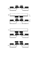
図14は補正電子光学系503の詳細を説明する図である。補正電子光学系503は、光軸に沿ってアパーチャアレイAA、ブランカーアレイBA、要素電子光学系アレイユニットLAU、ストッパーアレイSAで構成される。図14の(A)は電子銃501側から補正電子光学系503を見た図、(B)はAA’断面図である。アパーチャアレイAAは図14(A)に示すように基板に複数の開口が規則正しく配列(8×8)形成され、照射される電子ビームを複数(64本)の電子ビームに分割する。ブランカーアレイBAはアパーチャアレイAAで分割された複数の電子ビームを個別に偏向する偏向器を一枚の基板上に複数並べて形成したものである。要素電子光学系アレイユニットLAUは、同一平面内に複数の電子レンズを2次元配列して形成した電子レンズアレイである第1電子光学系アレイLA1、及び第2電子光学系アレイLA2で構成される。これら各電子光学系アレイLA1, LA2は上述の実施例で説明した構造を備え、上述する方法で作製されたものである。要素電子光学系アレイユニットLAUは共通のZ方向の軸に並ぶ、第1電子レンズアレイLA1の電子レンズと第2電子レンズアレイLA2の電子レンズとで一つの要素電子光学系ELを構成する。ストッパーアレイSAは、アパーチャーアレイAAと同様に基板に複数の開口が形成されている。そして、ブランカーアレイBAで偏向されたビームだけがストッパーアレイSAで遮断され、ブランカーアレイの制御によって各ビーム個別に、ウエハ505へのビーム入射のON/OFFの切り替えがなされる。
【0031】
本実施例の荷電粒子線露光装置によれば、補正電子光学系に上記説明したような優れた電子光学系アレイを用いることで、極めて露光精度の高い装置を提供することでき、これによって製造するデバイスの集積度を従来以上に向上させることができる。
【0032】
<半導体生産システムの実施例>
次に、上記露光装置を用いた半導体デバイス(ICやLSI等の半導体チップ、液晶パネル、CCD、薄膜磁気ヘッド、マイクロマシン等)の生産システムの例を説明する。これは半導体製造工場に設置された製造装置のトラブル対応や定期メンテナンス、あるいはソフトウェア提供などの保守サービスを、製造工場外のコンピュータネットワークを利用して行うものである。
【0033】
図15は全体システムをある角度から切り出して表現したものである。図中、101は半導体デバイスの製造装置を提供するベンダー(装置供給メーカー)の事業所である。製造装置の実例として、半導体製造工場で使用する各種プロセス用の半導体製造装置、例えば、前工程用機器(露光装置、レジスト処理装置、エッチング装置等のリソグラフィ装置、熱処理装置、成膜装置、平坦化装置等)や後工程用機器(組立て装置、検査装置等)を想定している。事業所101内には、製造装置の保守データベースを提供するホスト管理システム108、複数の操作端末コンピュータ110、これらを結ぶんでイントラネットを構築するローカルエリアネットワーク(LAN)109を備える。ホスト管理システム108は、LAN109を事業所の外部ネットワークであるインターネット105に接続するためのゲートウェイと、外部からのアクセスを制限するセキュリティ機能を備える。
【0034】
一方、102〜104は、製造装置のユーザーとしての半導体製造メーカーの製造工場である。製造工場102〜104は、互いに異なるメーカーに属する工場であっても良いし、同一のメーカーに属する工場(例えば、前工程用の工場、後工程用の工場等)であっても良い。各工場102〜104内には、夫々、複数の製造装置106と、それらを結んでイントラネットを構築するローカルエリアネットワーク(LAN)111と、各製造装置106の稼動状況を監視する監視装置としてホスト管理システム107とが設けられている。各工場102〜104に設けられたホスト管理システム107は、各工場内のLAN111を工場の外部ネットワークであるインターネット105に接続するためのゲートウェイを備える。これにより各工場のLAN111からインターネット105を介してベンダー101側のホスト管理システム108にアクセスが可能となり、ホスト管理システム108のセキュリティ機能によって限られたユーザーだけがアクセスが許可となっている。具体的には、インターネット105を介して、各製造装置106の稼動状況を示すステータス情報(例えば、トラブルが発生した製造装置の症状)を工場側からベンダー側に通知する他、その通知に対応する応答情報(例えば、トラブルに対する対処方法を指示する情報、対処用のソフトウェアやデータ)や、最新のソフトウェア、ヘルプ情報などの保守情報をベンダー側から受け取ることができる。各工場102〜104とベンダー101との間のデータ通信および各工場内のLAN111でのデータ通信には、インターネットで一般的に使用されている通信プロトコル(TCP/IP)が使用される。なお、工場外の外部ネットワークとしてインターネットを利用する代わりに、第三者からのアクセスができずにセキュリティの高い専用線ネットワーク(ISDNなど)を利用することもできる。また、ホスト管理システムはベンダーが提供するものに限らずユーザーがデータベースを構築して外部ネットワーク上に置き、ユーザーの複数の工場から該データベースへのアクセスを許可するようにしてもよい。
【0035】
さて、図16は本実施形態の全体システムを図15とは別の角度から切り出して表現した概念図である。先の例ではそれぞれが製造装置を備えた複数のユーザー工場と、該製造装置のベンダーの管理システムとを外部ネットワークで接続して、該外部ネットワークを介して各工場の生産管理や少なくとも1台の製造装置の情報をデータ通信するものであった。これに対し本例は、複数のベンダーの製造装置を備えた工場と、該複数の製造装置のそれぞれのベンダーの管理システムとを工場外の外部ネットワークで接続して、各製造装置の保守情報をデータ通信するものである。図中、201は製造装置ユーザー(半導体デバイス製造メーカー)の製造工場であり、工場の製造ラインには各種プロセスを行う製造装置、ここでは例として露光装置202、レジスト処理装置203、成膜処理装置204が導入されている。なお図16では製造工場201は1つだけ描いているが、実際は複数の工場が同様にネットワーク化されている。工場内の各装置はLAN206で接続されてイントラネットを構成し、ホスト管理システム205で製造ラインの稼動管理がされている。一方、露光装置メーカー210、レジスト処理装置メーカー220、成膜装置メーカー230などベンダー(装置供給メーカー)の各事業所には、それぞれ供給した機器の遠隔保守を行なうためのホスト管理システム211,221,231を備え、これらは上述したように保守データベースと外部ネットワークのゲートウェイを備える。ユーザーの製造工場内の各装置を管理するホスト管理システム205と、各装置のベンダーの管理システム211,221,231とは、外部ネットワーク200であるインターネットもしくは専用線ネットワークによって接続されている。このシステムにおいて、製造ラインの一連の製造機器の中のどれかにトラブルが起きると、製造ラインの稼動が休止してしまうが、トラブルが起きた機器のベンダーからインターネット200を介した遠隔保守を受けることで迅速な対応が可能で、製造ラインの休止を最小限に抑えることができる。
【0036】
半導体製造工場に設置された各製造装置はそれぞれ、ディスプレイと、ネットワークインターフェースと、記憶装置にストアされたネットワークアクセス用ソフトウェアならびに装置動作用のソフトウェアを実行するコンピュータを備える。記憶装置としては内蔵メモリやハードディスク、あるいはネットワークファイルサーバーなどである。上記ネットワークアクセス用ソフトウェアは、専用又は汎用のウェブブラウザを含み、例えば図17に一例を示す様な画面のユーザーインターフェースをディスプレイ上に提供する。各工場で製造装置を管理するオペレータは、画面を参照しながら、製造装置の機種(401)、シリアルナンバー(402)、トラブルの件名(403)、発生日(404)、緊急度(405)、症状(406)、対処法(407)、経過(408)等の情報を画面上の入力項目に入力する。入力された情報はインターネットを介して保守データベースに送信され、その結果の適切な保守情報が保守データベースから返信されディスプレイ上に提示される。またウェブブラウザが提供するユーザーインターフェースはさらに図示のごとくハイパーリンク機能(410〜412)を実現し、オペレータは各項目の更に詳細な情報にアクセスしたり、ベンダーが提供するソフトウェアライブラリから製造装置に使用する最新バージョンのソフトウェアを引出したり、工場のオペレータの参考に供する操作ガイド(ヘルプ情報)を引出したりすることができる。
【0037】
次に上記説明した生産システムを利用した半導体デバイスの製造プロセスを説明する。図18は半導体デバイスの全体的な製造プロセスのフローを示す。ステップ1(回路設計)では半導体デバイスの回路設計を行なう。ステップ2(露光制御データ作製)では設計した回路パターンに基づいて露光装置の露光制御データを作製する。一方、ステップ3(ウエハ製造)ではシリコン等の材料を用いてウエハを製造する。ステップ4(ウエハプロセス)は前工程と呼ばれ、上記用意したマスクとウエハを用いて、リソグラフィ技術によってウエハ上に実際の回路を形成する。次のステップ5(組み立て)は後工程と呼ばれ、ステップ4によって作製されたウエハを用いて半導体チップ化する工程であり、アッセンブリ工程(ダイシング、ボンディング)、パッケージング工程(チップ封入)等の組立て工程を含む。ステップ6(検査)ではステップ5で作製された半導体デバイスの動作確認テスト、耐久性テスト等の検査を行なう。こうした工程を経て半導体デバイスが完成し、これを出荷(ステップ7)する。前工程と後工程はそれぞれ専用の別の工場で行い、これらの工場毎に上記説明した遠隔保守システムによって保守がなされる。また前工程工場と後工程工場との間でも、インターネットまたは専用線ネットワークを介して生産管理や装置保守のための情報がデータ通信される。
【0038】
図19は上記ウエハプロセスの詳細なフローを示す。ステップ11(酸化)ではウエハの表面を酸化させる。ステップ12(CVD)ではウエハ表面に絶縁膜を成膜する。ステップ13(電極形成)ではウエハ上に電極を蒸着によって形成する。ステップ14(イオン打込み)ではウエハにイオンを打ち込む。ステップ15(レジスト処理)ではウエハに感光剤を塗布する。ステップ16(露光)では上記説明した露光装置によってマスクの回路パターンをウエハに焼付露光する。ステップ17(現像)では露光したウエハを現像する。ステップ18(エッチング)では現像したレジスト像以外の部分を削り取る。ステップ19(レジスト剥離)ではエッチングが済んで不要となったレジストを取り除く。これらのステップを繰り返し行なうことによって、ウエハ上に多重に回路パターンを形成する。各工程で使用する製造機器は上記説明した遠隔保守システムによって保守がなされているので、トラブルを未然に防ぐと共に、もしトラブルが発生しても迅速な復旧が可能で、従来に比べて半導体デバイスの生産性を向上させることができる。
【0039】
【発明の効果】
本発明によれば、クロストークを軽減した荷電粒子光学系アレイを提供することができる。そして、これを含む荷電粒子線露光装置、および、当該荷電粒子線露光装置を利用したデバイス製造方法を提供することができる。
【図面の簡単な説明】
【図1】電子光学系アレイの構造を説明する図
【図2】上電極(下電極)とシールド電極の作製方法を説明する図
【図3】中間電極の作製方法を説明する図
【図4】電極同士の接合の方法をを説明する図
【図5】電極同士の接合が完成した状態を説明する図
【図6】電子光学系アレイの別例の構造を説明する図
【図7】電子光学系アレイの別例の構造を説明する図
【図8】電子光学系アレイの別例の構造を説明する図
【図9】電子光学系アレイの別例の構造を説明する図
【図10】クロストークの発生を説明する図
【図11】電子光学系アレイの別例の構造を説明する図
【図12】電子光学系アレイの別例の構造を説明する図
【図13】マルチビーム型露光装置の全体図
【図14】補正電子光学系の詳細を説明する図
【図15】半導体デバイス生産システムの例をある角度から見た概念図
【図16】半導体デバイス生産システムの例を別の角度から見た概念図
【図17】ディスプレイ上のユーザーインターフェースを示す図
【図18】半導体デバイスの製造プロセスのフローを説明する図
【図19】ウエハプロセスの詳細を説明する図
【符号の説明】
1 上電極
2 中間電極
3 下電極
4 上シールド電極
5 下シールド電極
6 絶縁膜
7 絶縁膜
8 上電極の開口
9 上シールド電極の開口
10 中間電極の開口
11 中間電極の個々の電極素子
12 配線
13 下シールド電極の開口
14 下電極の開口[0001]
BACKGROUND OF THE INVENTION
The present invention,pluralCharged particlesThe optical system is an arrayCharged particlesThe present invention relates to an optical system array.
[0002]
[Prior art]
In the production of semiconductor devices, the electron beam exposure technique has been spotlighted as a promising candidate for lithography that enables fine pattern exposure of 0.1 μm or less, and there are several methods. For example, there is a variable rectangular beam method that draws a pattern by so-called one-stroke drawing. However, this has a low throughput and has many problems as an exposure machine for mass production. In order to improve the throughput, a figure batch exposure method has been proposed in which a pattern formed on a stencil mask is reduced and transferred. This method is advantageous for simple patterns with many repetitions, but random patterns such as a logic wiring layer have many problems in terms of throughput, and greatly impede productivity improvement in practical use.
[0003]
In contrast, a multi-beam system that simultaneously draws a pattern with multiple electron beams without using a mask has been proposed, which eliminates the need for physical mask fabrication and replacement, and has many advantages for practical use. I have. What is important in making an electron beam multi-purpose is the number of arrays of electron lenses used for this. The number of beams is determined by the number of electron lens arrays that can be arranged inside the electron beam exposure apparatus, which is a major factor in determining the throughput. Therefore, one of the keys to improving the performance of the multi-beam type exposure apparatus is how to reduce the size while enhancing the performance of the electron lens.
[0004]
Electron lenses are classified into an electromagnetic type and an electrostatic type, and the electrostatic type is easy to configure and advantageous for miniaturization as compared with the magnetic type without the need for providing a coil core or the like. Here, main technologies related to miniaturization of the electrostatic electron lens (electrostatic lens) are shown below.
[0005]
AD Feinerman et al. (J. Vac. Sci. Technol. A 10 (4), p611, 1992) developed an electrostatic monolithic technique using micromechanical technology using V-grooves fabricated by crystal anisotropic etching of fiber and Si. Disclosed is the formation of a three-dimensional structure consisting of three electrodes, which are lenses. Si is provided with a membrane frame, a membrane, and an opening through which the electron beam passes. In addition, KY Lee et al. (J. Vac. Sci. Technol. B 12 (6), p3425, 1994) disclose a structure in which Si and Pyrex glass are bonded in a plurality of layers using an anodic bonding method. Thus, an electron lens for microcolumn aligned with high accuracy is manufactured. Sasaki (J. Vac. Sci. Technol. 19, 963 (1981)) discloses a configuration in which an Einzel lens array is formed by three electrodes having a lens aperture array. Chang et al. (J. Vac. Sci. Technol. B10, 2743 (1992)) have proposed a configuration in which a plurality of microcolumns having Einzel lenses are arranged.
[0006]
[Problems to be solved by the invention]
However, in the above conventional example, when a large number of aperture electrodes are arranged in an array and each electron beam is to have a different lens action, the trajectory and aberration change due to the influence of the surrounding electrostatic lens electric field. There is a possibility that a so-called crosstalk problem that becomes difficult to operate independently may occur.
[0007]
This crosstalk problem will be specifically described with reference to FIG. An Einzel lens is constituted by the three electrodes of the
[0008]
The present inventionofOne of the purposes is,Reduced crosstalkCharged particlesIs to provide an optical system array.
[0009]
[Means for Solving the Problems]
BookinventionFirst charged particle optics arrayAre each formed with multiple openingsAnd each otherStacked first electrodeandSecond electrode, first electrode and second electrodeWhenBetweenInA shield electrode provided corresponding to each of the plurality of openings;,It is characterized by havingCharged particlesIt is an optical system array.
[0010]
The present inventionSecond charged particle optics arrayAre each formed with multiple openingsAnd each otherLaminated upper electrode, intermediate electrode and lower electrode, and upper electrode and intermediate electrodeWhenBetween the intermediate electrode and the lower electrodeWhenBetweenIn each ofA shield electrode provided corresponding to each of the plurality of openings;,It is characterized by havingCharged particlesIt is an optical system array.
[0011]
Of the present inventionCharged particle beam exposure systemIsAn exposure apparatus that exposes a wafer with a plurality of charged particle beams,AboveMultiple charged particle beamsFormCharged particlesOptical systemTheYesThe charged particle optical system includes the charged particle optical system array according to any one of
[0012]
Of the present inventionDevice manufacturing methodThe above-mentioned exposure apparatusUsing the step of exposing the substrate and developing the substrate exposed in the stepThis is a device manufacturing method.
[0013]
DETAILED DESCRIPTION OF THE INVENTION
<Electron optical system array>
An electron optical system array according to an embodiment of the present invention will be described with reference to the drawings. FIG. 1 is an exploded view of an electron optical system array. In the figure, there is a large structure in which an
[0014]
In the electron optical system array having the above-described configuration, a potential of 0 [V] is applied to the
[0015]
Next, a method for producing the electron optical system array having the above structure will be described. Here, in order to simplify the explanation, only one opening is closed up.
[0016]
First, a method for producing the
[0017]
First, a silicon wafer having a crystal orientation of <100> is prepared as a substrate, and silicon nitride having a film thickness of 300 nm is formed by chemical vapor deposition (FIG. 2A). Through the resist process and the etching process, the silicon nitride film is removed from the part that will later become the optical path of the electron beam and the part to be aligned between the electrodes. Next, the silicon substrate in the opening is anisotropically etched with a tetramethylammonium hydroxide aqueous solution to a depth of about 1 to 2 μm to form a V-shaped V groove on at least one surface of the substrate. Next, chromium / gold is continuously deposited as an upper electrode in a thickness of 50 nm / 1 μm on the surface where the V-groove is formed, and after resist patterning, the gold / chromium is etched to form an electron beam opening (see FIG. 2 (b)). Next, a
[0018]
The production method of the
[0019]
A method of joining the lower electrode and the intermediate electrode will be described with reference to FIG. A lower electrode and a lower shield electrode (f) prepared by the procedure of FIG. 2 are prepared. A
[0020]
FIG. 5 is a diagram for explaining the final assembly. The bonded lower electrode / lower shield electrode / intermediate electrode produced in FIG. 4 (d) and the upper electrode / upper shield electrode produced in FIG. 2 (f) face each other, and are formed on both substrates. Positioning is achieved in a direction perpendicular to the direction parallel to the bonding surface by installing the
[0021]
Next, some modifications of the above-described electron optical system array will be described. FIG. 6 is an exploded view showing a configuration example having a plurality of intermediate electrodes. In contrast to the example of FIG. 1 in which the number of intermediate electrodes is one, the
[0022]
FIG. 7 shows an example in which the shield electrode is integrally formed as one electrode without being separated. That is, the
[0023]
FIG. 8 shows another example of the structure. An intermediate shield electrode is disposed in the gap between the plurality of cylindrical electrode elements of the intermediate electrode. An
[0024]
FIG. 9 shows still another structural example. The intermediate electrode has a plurality of
[0025]
FIG. 11 is a view showing an electron lens array of still another form. FIG. 11A is a cross-sectional view of the lens array, which includes an
[0026]
In order to effectively reduce the crosstalk, as shown in FIG. 11A, the interval s between the
[0027]
Figure11An intermediate electrode structure as shown in FIG. In the figure, the
[0028]
FIG. 12 shows a further modification. The unit LA1 including the
[0029]
<Electron beam exposure system>
Next, an embodiment of a multi-beam type charged particle exposure apparatus (electron beam exposure apparatus) will be described as an example of a system using the electron optical system array. FIG. 13 is a schematic diagram of the entire system. In the figure, an
[0030]
FIG. 14 is a diagram for explaining the details of the correction electron
[0031]
According to the charged particle beam exposure apparatus of the present embodiment, by using the excellent electron optical system array as described above for the correction electron optical system, an apparatus with extremely high exposure accuracy can be provided and manufactured by this. The degree of device integration can be improved more than before.
[0032]
<Example of semiconductor production system>
Next, an example of a production system of a semiconductor device (a semiconductor chip such as an IC or LSI, a liquid crystal panel, a CCD, a thin film magnetic head, a micromachine, etc.) using the exposure apparatus will be described. In this method, maintenance services such as troubleshooting, periodic maintenance, and software provision for manufacturing apparatuses installed in a semiconductor manufacturing factory are performed using a computer network outside the manufacturing factory.
[0033]
FIG. 15 illustrates the entire system cut out from a certain angle. In the figure,
[0034]
On the other hand,
[0035]
FIG. 16 is a conceptual diagram showing the overall system of this embodiment cut out from an angle different from that in FIG. In the previous example, a plurality of user factories each equipped with a manufacturing device and a management system of a vendor of the manufacturing device are connected by an external network, and production control of each factory or at least one unit is performed via the external network. Data communication of manufacturing equipment was performed. On the other hand, in this example, a factory equipped with a plurality of vendors' manufacturing devices and a management system of each vendor of the plurality of manufacturing devices are connected via an external network outside the plant, and maintenance information for each manufacturing device is obtained. Data communication. In the figure,
[0036]
Each manufacturing apparatus installed in the semiconductor manufacturing factory includes a display, a network interface, a computer for executing network access software stored in a storage device and software for operating the apparatus. The storage device is a built-in memory, a hard disk, or a network file server. The network access software includes a dedicated or general-purpose web browser, and provides, for example, a user interface having a screen as shown in FIG. 17 on the display. The operator who manages the manufacturing equipment in each factory, while referring to the screen, the manufacturing equipment model (401), serial number (402), trouble subject (403), date of occurrence (404), urgency (405), Information such as symptom (406), coping method (407), progress (408), etc. is input to the input items on the screen. The input information is transmitted to the maintenance database via the Internet, and appropriate maintenance information as a result is returned from the maintenance database and presented on the display. The user interface provided by the web browser further realizes a hyperlink function (410 to 412) as shown in the figure. Operators can access more detailed information on each item or use the software library provided by the vendor for manufacturing equipment. The latest version of software can be pulled out, and operation guides (help information) can be pulled out for reference by factory operators.
[0037]
Next, a semiconductor device manufacturing process using the production system described above will be described. FIG. 18 shows the flow of the entire manufacturing process of the semiconductor device. In step 1 (circuit design), the semiconductor device circuit is designed. In step 2 (exposure control data creation), exposure control data for the exposure apparatus is created based on the designed circuit pattern. On the other hand, in step 3 (wafer manufacture), a wafer is manufactured using a material such as silicon. Step 4 (wafer process) is called a pre-process, and an actual circuit is formed on the wafer by lithography using the prepared mask and wafer. The next step 5 (assembly) is called a post-process, and is a process for forming a semiconductor chip using the wafer produced in
[0038]
FIG. 19 shows a detailed flow of the wafer process. In step 11 (oxidation), the wafer surface is oxidized. In step 12 (CVD), an insulating film is formed on the wafer surface. In step 13 (electrode formation), an electrode is formed on the wafer by vapor deposition. In step 14 (ion implantation), ions are implanted into the wafer. In step 15 (resist process), a photosensitive agent is applied to the wafer. In step 16 (exposure), the circuit pattern of the mask is printed on the wafer by exposure using the exposure apparatus described above. In step 17 (development), the exposed wafer is developed. In step 18 (etching), portions other than the developed resist image are removed. In step 19 (resist stripping), the unnecessary resist after etching is removed. By repeating these steps, multiple circuit patterns are formed on the wafer. Since the manufacturing equipment used in each process is maintained by the remote maintenance system described above, it is possible to prevent problems before they occur, and to recover quickly if a problem occurs. Productivity can be improved.
[0039]
【The invention's effect】
According to the present invention,Cross talkReduced charged particlesAn optical system array can be provided. And thisIncluding charged particle beamExposure equipment,And using the charged particle beam exposure apparatusDevice manufacturing methodTheCan be provided.
[Brief description of the drawings]
FIG. 1 is a diagram illustrating the structure of an electron optical system array
FIG. 2 is a view for explaining a method for producing an upper electrode (lower electrode) and a shield electrode
FIG. 3 is a diagram illustrating a method for manufacturing an intermediate electrode
FIG. 4 is a diagram illustrating a method for joining electrodes together
FIG. 5 is a diagram for explaining a state in which the joining of electrodes is completed
FIG. 6 is a diagram for explaining the structure of another example of an electron optical system array;
FIG. 7 is a view for explaining the structure of another example of an electron optical system array;
FIG. 8 is a diagram for explaining the structure of another example of an electron optical system array;
FIG. 9 is a diagram for explaining the structure of another example of an electron optical system array;
FIG. 10 is a diagram for explaining the occurrence of crosstalk.
FIG. 11 is a diagram for explaining the structure of another example of an electron optical system array;
FIG. 12 is a diagram for explaining the structure of another example of an electron optical system array;
FIG. 13 is an overall view of a multi-beam type exposure apparatus.
FIG. 14 is a diagram for explaining details of a correction electron optical system.
FIG. 15 is a conceptual diagram of an example of a semiconductor device production system viewed from a certain angle.
FIG. 16 is a conceptual diagram of an example of a semiconductor device production system viewed from another angle.
FIG. 17 shows a user interface on the display.
FIG. 18 is a diagram for explaining the flow of a semiconductor device manufacturing process;
FIG. 19 is a diagram for explaining the details of the wafer process;
[Explanation of symbols]
1 Upper electrode
2 Intermediate electrode
3 Lower electrode
4 Upper shield electrode
5 Lower shield electrode
6 Insulating film
7 Insulating film
8 Upper electrode opening
9 Opening of upper shield electrode
10 Opening of the intermediate electrode
11 Individual electrode elements of the intermediate electrode
12 Wiring
13 Opening of lower shield electrode
14 Opening of lower electrode
Claims (16)
Priority Applications (4)
| Application Number | Priority Date | Filing Date | Title |
|---|---|---|---|
| JP2000233145A JP4585661B2 (en) | 2000-03-31 | 2000-08-01 | Electro-optical array, charged particle beam exposure apparatus, and device manufacturing method |
| US09/819,737 US6965153B1 (en) | 2000-03-31 | 2001-03-29 | Electrooptic system array, charged-particle beam exposure apparatus using the same, and device manufacturing method |
| US10/454,576 US7038226B2 (en) | 2000-03-31 | 2003-06-05 | Electrooptic system array, charged-particle beam exposure apparatus using the same, and device manufacturing method |
| US11/168,425 US7126141B2 (en) | 2000-03-31 | 2005-06-29 | Electrooptic system array, charged-particle beam exposure apparatus using the same, and device manufacturing method |
Applications Claiming Priority (3)
| Application Number | Priority Date | Filing Date | Title |
|---|---|---|---|
| JP2000-97069 | 2000-03-31 | ||
| JP2000097069 | 2000-03-31 | ||
| JP2000233145A JP4585661B2 (en) | 2000-03-31 | 2000-08-01 | Electro-optical array, charged particle beam exposure apparatus, and device manufacturing method |
Publications (3)
| Publication Number | Publication Date |
|---|---|
| JP2001345259A JP2001345259A (en) | 2001-12-14 |
| JP2001345259A5 JP2001345259A5 (en) | 2007-09-13 |
| JP4585661B2 true JP4585661B2 (en) | 2010-11-24 |
Family
ID=26589083
Family Applications (1)
| Application Number | Title | Priority Date | Filing Date |
|---|---|---|---|
| JP2000233145A Expired - Fee Related JP4585661B2 (en) | 2000-03-31 | 2000-08-01 | Electro-optical array, charged particle beam exposure apparatus, and device manufacturing method |
Country Status (2)
| Country | Link |
|---|---|
| US (3) | US6965153B1 (en) |
| JP (1) | JP4585661B2 (en) |
Families Citing this family (75)
| Publication number | Priority date | Publication date | Assignee | Title |
|---|---|---|---|---|
| JP4947842B2 (en) * | 2000-03-31 | 2012-06-06 | キヤノン株式会社 | Charged particle beam exposure system |
| JP2001284230A (en) * | 2000-03-31 | 2001-10-12 | Canon Inc | Electronic optical system array, charged particle beam exposure system provided therewith, and method of manufacturing device |
| JP2001283756A (en) * | 2000-03-31 | 2001-10-12 | Canon Inc | Electron optical system array, charged particle beam exposure device using it and device manufacturing method |
| JP4585661B2 (en) * | 2000-03-31 | 2010-11-24 | キヤノン株式会社 | Electro-optical array, charged particle beam exposure apparatus, and device manufacturing method |
| JP4947841B2 (en) * | 2000-03-31 | 2012-06-06 | キヤノン株式会社 | Charged particle beam exposure system |
| JP2002217089A (en) * | 2001-01-18 | 2002-08-02 | Advantest Corp | Electron beam deflector, its manufacturing method and electron beam aligner |
| JP4246401B2 (en) * | 2001-01-18 | 2009-04-02 | 株式会社アドバンテスト | Electron beam exposure apparatus and electron beam deflection apparatus |
| EP2434522B8 (en) * | 2002-07-16 | 2014-07-23 | Canon Kabushiki Kaisha | Multi-charged beam lens, charged-particle beam exposure apparatus using the same, and device manufacturing method |
| JP2004282038A (en) * | 2003-02-28 | 2004-10-07 | Canon Inc | Deflector, method for producing deflector, and charged particle beam exposure device using deflector |
| EP1463087B1 (en) * | 2003-03-24 | 2010-06-02 | ICT, Integrated Circuit Testing Gesellschaft für Halbleiterprüftechnik Mbh | Charged particle beam device |
| JP4459568B2 (en) * | 2003-08-06 | 2010-04-28 | キヤノン株式会社 | Multi charged beam lens and charged beam exposure apparatus using the same |
| EP2579274A1 (en) | 2003-09-05 | 2013-04-10 | Carl Zeiss SMT GmbH | Particle-optical systems and arrangements and particle-optical components for such systems and arrangements |
| CN101019203B (en) * | 2004-05-17 | 2010-12-22 | 迈普尔平版印刷Ip有限公司 | Charged particle beam exposure system |
| US7102185B2 (en) * | 2004-06-21 | 2006-09-05 | Eastman Kodak Company | Lightshield architecture for interline transfer image sensors |
| JP4541798B2 (en) * | 2004-08-06 | 2010-09-08 | キヤノン株式会社 | Charged particle beam lens array, and charged particle beam exposure apparatus using the charged particle beam lens array |
| JP4738822B2 (en) * | 2005-01-26 | 2011-08-03 | キヤノン株式会社 | Electrostatic lens apparatus and adjustment method thereof, charged particle beam exposure apparatus, and device manufacturing method |
| JP4657740B2 (en) * | 2005-01-26 | 2011-03-23 | キヤノン株式会社 | Aberration measuring apparatus for charged particle beam optical system, charged particle beam exposure apparatus including the aberration measuring apparatus, and device manufacturing method using the apparatus |
| JP4648087B2 (en) * | 2005-05-25 | 2011-03-09 | キヤノン株式会社 | Deflector fabrication method, charged particle beam exposure apparatus, and device manufacturing method |
| EP1753010B1 (en) | 2005-08-09 | 2012-12-05 | Carl Zeiss SMS GmbH | Particle-optical system |
| JP2007231324A (en) * | 2006-02-28 | 2007-09-13 | Canon Inc | Multiple charged particle beam-machining apparatus |
| KR100809277B1 (en) * | 2006-07-05 | 2008-03-03 | 삼성전기주식회사 | Camer module having a array lens |
| JP5048283B2 (en) * | 2006-07-20 | 2012-10-17 | キヤノン株式会社 | Deflector array, drawing apparatus, and device manufacturing method |
| CN101496129B (en) * | 2006-07-25 | 2017-06-23 | 迈普尔平版印刷Ip有限公司 | multiple beam charged particle optical system |
| US8134135B2 (en) | 2006-07-25 | 2012-03-13 | Mapper Lithography Ip B.V. | Multiple beam charged particle optical system |
| JP2008066359A (en) * | 2006-09-05 | 2008-03-21 | Canon Inc | Charged particle beam lens array, exposure apparatus and method of manufacturing device |
| US7669985B2 (en) * | 2007-04-23 | 2010-03-02 | Xerox Corporation | Jetstack plate to plate alignment |
| EP2019415B1 (en) * | 2007-07-24 | 2016-05-11 | IMS Nanofabrication AG | Multi-beam source |
| EP2251893B1 (en) * | 2009-05-14 | 2014-10-29 | IMS Nanofabrication AG | Multi-beam deflector array means with bonded electrodes |
| JP5669636B2 (en) * | 2011-03-15 | 2015-02-12 | キヤノン株式会社 | Charged particle beam lens and exposure apparatus using the same |
| JP2012195095A (en) * | 2011-03-15 | 2012-10-11 | Canon Inc | Manufacturing method of charged particle beam lens |
| JP2012195097A (en) * | 2011-03-15 | 2012-10-11 | Canon Inc | Charged particle beam lens and exposure apparatus using the same |
| NL2007604C2 (en) * | 2011-10-14 | 2013-05-01 | Mapper Lithography Ip Bv | Charged particle system comprising a manipulator device for manipulation of one or more charged particle beams. |
| NL2006868C2 (en) | 2011-05-30 | 2012-12-03 | Mapper Lithography Ip Bv | Charged particle multi-beamlet apparatus. |
| JP2013084638A (en) * | 2011-10-05 | 2013-05-09 | Canon Inc | Electrostatic lens |
| EP2629317B1 (en) * | 2012-02-20 | 2015-01-28 | ICT Integrated Circuit Testing Gesellschaft für Halbleiterprüftechnik mbH | Charged particle beam device with dynamic focus and method of operating thereof |
| JP2013239667A (en) * | 2012-05-17 | 2013-11-28 | Canon Inc | Electrode of charged particle beam electrostatic lens and manufacturing method of the same, charged particle beam electrostatic lens, and charged particle beam exposure device |
| EP2757571B1 (en) * | 2013-01-17 | 2017-09-20 | IMS Nanofabrication AG | High-voltage insulation device for charged-particle optical apparatus |
| JP2014229841A (en) * | 2013-05-24 | 2014-12-08 | キヤノン株式会社 | Drawing device and method of manufacturing article |
| JP2015023286A (en) | 2013-07-17 | 2015-02-02 | アイエムエス ナノファブリケーション アーゲー | Pattern definition device having multiple blanking arrays |
| EP2830083B1 (en) | 2013-07-25 | 2016-05-04 | IMS Nanofabrication AG | Method for charged-particle multi-beam exposure |
| EP2913838B1 (en) | 2014-02-28 | 2018-09-19 | IMS Nanofabrication GmbH | Compensation of defective beamlets in a charged-particle multi-beam exposure tool |
| US9443699B2 (en) | 2014-04-25 | 2016-09-13 | Ims Nanofabrication Ag | Multi-beam tool for cutting patterns |
| EP3358599B1 (en) | 2014-05-30 | 2021-01-27 | IMS Nanofabrication GmbH | Compensation of dose inhomogeneity using row calibration |
| JP6892214B2 (en) | 2014-07-10 | 2021-06-23 | アイエムエス ナノファブリケーション ゲーエムベーハー | Customization of particle beam lithography system using convolution kernel |
| US9568907B2 (en) | 2014-09-05 | 2017-02-14 | Ims Nanofabrication Ag | Correction of short-range dislocations in a multi-beam writer |
| DE102015202172B4 (en) | 2015-02-06 | 2017-01-19 | Carl Zeiss Microscopy Gmbh | Particle beam system and method for particle-optical examination of an object |
| US9653263B2 (en) | 2015-03-17 | 2017-05-16 | Ims Nanofabrication Ag | Multi-beam writing of pattern areas of relaxed critical dimension |
| EP3096342B1 (en) | 2015-03-18 | 2017-09-20 | IMS Nanofabrication AG | Bi-directional double-pass multi-beam writing |
| US10410831B2 (en) | 2015-05-12 | 2019-09-10 | Ims Nanofabrication Gmbh | Multi-beam writing using inclined exposure stripes |
| US10325756B2 (en) | 2016-06-13 | 2019-06-18 | Ims Nanofabrication Gmbh | Method for compensating pattern placement errors caused by variation of pattern exposure density in a multi-beam writer |
| US10325757B2 (en) | 2017-01-27 | 2019-06-18 | Ims Nanofabrication Gmbh | Advanced dose-level quantization of multibeam-writers |
| US10522329B2 (en) | 2017-08-25 | 2019-12-31 | Ims Nanofabrication Gmbh | Dose-related feature reshaping in an exposure pattern to be exposed in a multi beam writing apparatus |
| US11569064B2 (en) | 2017-09-18 | 2023-01-31 | Ims Nanofabrication Gmbh | Method for irradiating a target using restricted placement grids |
| KR102649183B1 (en) * | 2017-10-02 | 2024-03-21 | 에이에스엠엘 네델란즈 비.브이. | An apparatus using charged particle beams |
| EP3474308A1 (en) * | 2017-10-17 | 2019-04-24 | Universiteit Antwerpen | Spatial phase manipulation of charged particle beam |
| US10651010B2 (en) | 2018-01-09 | 2020-05-12 | Ims Nanofabrication Gmbh | Non-linear dose- and blur-dependent edge placement correction |
| US10840054B2 (en) | 2018-01-30 | 2020-11-17 | Ims Nanofabrication Gmbh | Charged-particle source and method for cleaning a charged-particle source using back-sputtering |
| DE102018202428B3 (en) | 2018-02-16 | 2019-05-09 | Carl Zeiss Microscopy Gmbh | Multibeam Teilchenmikroskop |
| DE102018202421B3 (en) | 2018-02-16 | 2019-07-11 | Carl Zeiss Microscopy Gmbh | Multibeam particle beam |
| WO2019166331A2 (en) | 2018-02-27 | 2019-09-06 | Carl Zeiss Microscopy Gmbh | Charged particle beam system and method |
| CN112055694B (en) * | 2018-04-25 | 2023-12-19 | 希奥检测有限公司 | Capacitive sensor with temperature stable output |
| US10811215B2 (en) | 2018-05-21 | 2020-10-20 | Carl Zeiss Multisem Gmbh | Charged particle beam system |
| DE102018007455B4 (en) | 2018-09-21 | 2020-07-09 | Carl Zeiss Multisem Gmbh | Process for detector alignment when imaging objects using a multi-beam particle microscope, system and computer program product |
| DE102018007652B4 (en) * | 2018-09-27 | 2021-03-25 | Carl Zeiss Multisem Gmbh | Particle beam system and method for current regulation of single particle beams |
| JP7207927B2 (en) * | 2018-09-28 | 2023-01-18 | 株式会社ディスコ | Semiconductor package manufacturing method |
| DE102018124044B3 (en) | 2018-09-28 | 2020-02-06 | Carl Zeiss Microscopy Gmbh | Method for operating a multi-beam particle beam microscope and multi-beam particle beam system |
| US11145485B2 (en) * | 2018-12-26 | 2021-10-12 | Nuflare Technology, Inc. | Multiple electron beams irradiation apparatus |
| CN111477530B (en) | 2019-01-24 | 2023-05-05 | 卡尔蔡司MultiSEM有限责任公司 | Method for imaging 3D samples using a multi-beam particle microscope |
| TWI743626B (en) | 2019-01-24 | 2021-10-21 | 德商卡爾蔡司多重掃描電子顯微鏡有限公司 | System comprising a multi-beam particle microscope, method for imaging a 3d sample layer by layer and computer program product |
| EP3828914A1 (en) * | 2019-02-27 | 2021-06-02 | FEI Company | Charged particle beam device for inspection of a specimen with a plurality of charged particle beamlets |
| US11099482B2 (en) | 2019-05-03 | 2021-08-24 | Ims Nanofabrication Gmbh | Adapting the duration of exposure slots in multi-beam writers |
| JP2023517626A (en) | 2020-03-12 | 2023-04-26 | カール ツァイス マルティセム ゲゼルシヤフト ミット ベシュレンクテル ハフツング | Specific improvements for multi-beam generation units and multi-beam deflection units |
| KR20210132599A (en) | 2020-04-24 | 2021-11-04 | 아이엠에스 나노패브릭케이션 게엠베하 | Chargedparticle source |
| KR20240042652A (en) | 2021-08-10 | 2024-04-02 | 칼 짜이스 멀티셈 게엠베하 | Multi-beam generation unit with increased focusing power |
| WO2023247067A1 (en) | 2022-06-23 | 2023-12-28 | Carl Zeiss Multisem Gmbh | Multi-beam system and multi-beam forming unit with reduced sensitivity to secondary radiation |
Family Cites Families (68)
| Publication number | Priority date | Publication date | Assignee | Title |
|---|---|---|---|---|
| US3755704A (en) * | 1970-02-06 | 1973-08-28 | Stanford Research Inst | Field emission cathode structures and devices utilizing such structures |
| US4200794A (en) | 1978-11-08 | 1980-04-29 | Control Data Corporation | Micro lens array and micro deflector assembly for fly's eye electron beam tubes using silicon components and techniques of fabrication and assembly |
| SE421832B (en) | 1979-04-18 | 1982-02-01 | Pharos Ab | DEVICE FOR REGISTERING THE TOPOGRAPHY OF THE CHARGED MASS IN A MACHINE |
| US4419182A (en) * | 1981-02-27 | 1983-12-06 | Veeco Instruments Inc. | Method of fabricating screen lens array plates |
| US4354111A (en) * | 1981-03-10 | 1982-10-12 | Veeco Instruments Incorporated | Screen lens array system |
| US4419580A (en) | 1981-06-26 | 1983-12-06 | Control Data Corporation | Electron beam array alignment means |
| US4607167A (en) | 1982-10-19 | 1986-08-19 | Varian Associates, Inc. | Charged particle beam lithography machine incorporating localized vacuum envelope |
| US4569033A (en) * | 1983-06-14 | 1986-02-04 | The United States Of America As Represented By The Secretary Of The Navy | Optical matrix-matrix multiplier based on outer product decomposition |
| US4742234A (en) * | 1985-09-27 | 1988-05-03 | American Telephone And Telegraph Company, At&T Bell Laboratories | Charged-particle-beam lithography |
| US5354695A (en) * | 1992-04-08 | 1994-10-11 | Leedy Glenn J | Membrane dielectric isolation IC fabrication |
| JP2523931B2 (en) | 1990-04-16 | 1996-08-14 | 富士通株式会社 | Blanking aperture manufacturing method |
| JP2837515B2 (en) | 1990-06-20 | 1998-12-16 | 富士通株式会社 | Electron beam exposure system |
| US5121234A (en) * | 1990-10-29 | 1992-06-09 | Honeywell Incorporated | Dichroic liquid crystal display with integral electroluminescent backlighting |
| DE69226553T2 (en) * | 1991-03-13 | 1998-12-24 | Fujitsu Ltd | Device and method for exposure by means of charge carrier beams |
| US6184850B1 (en) * | 1991-09-04 | 2001-02-06 | Canon Kabushiki Kaisha | Image display apparatus with backlit display and method of driving the same |
| JPH0644093A (en) | 1992-04-01 | 1994-02-18 | Nec Corp | System for changing-over duplicating device |
| WO1994011896A1 (en) * | 1992-11-06 | 1994-05-26 | Mitsubishi Denki Kabushiki Kaisha | Image display |
| US5324930A (en) * | 1993-04-08 | 1994-06-28 | Eastman Kodak Company | Lens array for photodiode device with an aperture having a lens region and a non-lens region |
| US5617131A (en) * | 1993-10-28 | 1997-04-01 | Kyocera Corporation | Image device having a spacer with image arrays disposed in holes thereof |
| US5838119A (en) * | 1994-01-18 | 1998-11-17 | Engle; Craig D. | Electronic charge store mechanism |
| US5534311A (en) * | 1995-05-31 | 1996-07-09 | The United States Of America As Represented By The Secretary Of The Navy | Production of structures by electrostatically-focused deposition |
| US5942761A (en) * | 1995-06-07 | 1999-08-24 | Tuli; Raja Singh | Enhancement methods and devices for reading a fingerprint image |
| JPH10511501A (en) * | 1995-10-18 | 1998-11-04 | フィリップス エレクトロニクス ネムローゼ フェンノートシャップ | Display system |
| JP2785788B2 (en) | 1996-01-19 | 1998-08-13 | 日本電気株式会社 | Batch mask mounting holder structure |
| JP3647128B2 (en) * | 1996-03-04 | 2005-05-11 | キヤノン株式会社 | Electron beam exposure apparatus and exposure method thereof |
| DE69738276T2 (en) | 1996-03-04 | 2008-04-03 | Canon K.K. | Electron beam exposure apparatus, exposure method and method of creating an object |
| JP3565652B2 (en) * | 1996-04-25 | 2004-09-15 | 富士通株式会社 | Transmission mask for charged particle beam exposure apparatus and exposure apparatus using the same |
| US5929454A (en) | 1996-06-12 | 1999-07-27 | Canon Kabushiki Kaisha | Position detection apparatus, electron beam exposure apparatus, and methods associated with them |
| JP3796317B2 (en) | 1996-06-12 | 2006-07-12 | キヤノン株式会社 | Electron beam exposure method and device manufacturing method using the same |
| JP3927620B2 (en) | 1996-06-12 | 2007-06-13 | キヤノン株式会社 | Electron beam exposure method and device manufacturing method using the same |
| US5981954A (en) | 1997-01-16 | 1999-11-09 | Canon Kabushiki Kaisha | Electron beam exposure apparatus |
| JPH10214779A (en) | 1997-01-31 | 1998-08-11 | Canon Inc | Electron beam exposure method and fabrication of device using that method |
| JP4018197B2 (en) * | 1997-07-02 | 2007-12-05 | キヤノン株式会社 | Electron beam exposure method and electron beam exposure apparatus |
| US6107636A (en) | 1997-02-07 | 2000-08-22 | Canon Kabushiki Kaisha | Electron beam exposure apparatus and its control method |
| US5886432A (en) | 1997-04-28 | 1999-03-23 | Ultratech Stepper, Inc. | Magnetically-positioned X-Y stage having six-degrees of freedom |
| US6274877B1 (en) | 1997-05-08 | 2001-08-14 | Canon Kabushiki Kaisha | Electron beam exposure apparatus |
| JP3478058B2 (en) | 1997-05-30 | 2003-12-10 | 株式会社日立製作所 | Charged particle beam drawing equipment |
| JPH10335223A (en) * | 1997-06-02 | 1998-12-18 | Canon Inc | Electron beam exposure method and system |
| JPH1126348A (en) * | 1997-07-02 | 1999-01-29 | Canon Inc | Method and apparatus for electron beam exposure |
| US6104035A (en) | 1997-06-02 | 2000-08-15 | Canon Kabushiki Kaisha | Electron-beam exposure apparatus and method |
| JP3787417B2 (en) | 1997-06-11 | 2006-06-21 | キヤノン株式会社 | Electron beam exposure method and electron beam exposure apparatus |
| US6013976A (en) * | 1997-07-30 | 2000-01-11 | Zenith Electronics Corporation | In-line SB electron gun with large and deep main lens apertures |
| KR19990062942A (en) | 1997-12-10 | 1999-07-26 | 히로시 오우라 | Charge particle beam exposure device |
| JPH11195589A (en) * | 1998-01-05 | 1999-07-21 | Canon Inc | Multiple electron beam exposure method and its apparatus, and manufacture of device |
| US6381072B1 (en) * | 1998-01-23 | 2002-04-30 | Proxemics | Lenslet array systems and methods |
| US6014200A (en) | 1998-02-24 | 2000-01-11 | Nikon Corporation | High throughput electron beam lithography system |
| JP4077933B2 (en) | 1998-06-24 | 2008-04-23 | キヤノン株式会社 | Multi-electron beam exposure method and apparatus, and device manufacturing method |
| JP2000030647A (en) | 1998-07-10 | 2000-01-28 | Advantest Corp | Charged particle beam exposure device |
| US6137103A (en) * | 1998-07-31 | 2000-10-24 | Lucent Technologies | Opto-mechanical components |
| JP2000181643A (en) | 1998-12-11 | 2000-06-30 | Canon Inc | Device and method for image formation |
| TW444224B (en) * | 1998-12-21 | 2001-07-01 | Koninkl Philips Electronics Nv | Electron gun and display device provided with an electron gun |
| JP4410871B2 (en) | 1999-03-25 | 2010-02-03 | キヤノン株式会社 | Charged particle beam exposure apparatus and device manufacturing method using the apparatus |
| JP2001076990A (en) | 1999-08-31 | 2001-03-23 | Canon Inc | Charged particle beam exposure system and method for controlling the same |
| US6693684B2 (en) * | 1999-09-15 | 2004-02-17 | Rainbow Displays, Inc. | Construction of large, robust, monolithic and monolithic-like, AMLCD displays with wide view angle |
| JP3763446B2 (en) | 1999-10-18 | 2006-04-05 | キヤノン株式会社 | Electrostatic lens, electron beam drawing apparatus, charged beam application apparatus, and device manufacturing method |
| JP2001126651A (en) | 1999-10-22 | 2001-05-11 | Hitachi Ltd | Apparatus for electron beam lithography |
| JP2001168016A (en) | 1999-12-13 | 2001-06-22 | Canon Inc | Device and system for exposing charged corpuscular beam, control method therefor and device producing method |
| JP2001168017A (en) | 1999-12-13 | 2001-06-22 | Canon Inc | Device and method for exposing charged corpuscular beam, determining method for control data and method for producing device by applying the same |
| US6566664B2 (en) * | 2000-03-17 | 2003-05-20 | Canon Kabushiki Kaisha | Charged-particle beam exposure apparatus and device manufacturing method |
| JP4585661B2 (en) | 2000-03-31 | 2010-11-24 | キヤノン株式会社 | Electro-optical array, charged particle beam exposure apparatus, and device manufacturing method |
| JP2001283756A (en) | 2000-03-31 | 2001-10-12 | Canon Inc | Electron optical system array, charged particle beam exposure device using it and device manufacturing method |
| JP2001284230A (en) | 2000-03-31 | 2001-10-12 | Canon Inc | Electronic optical system array, charged particle beam exposure system provided therewith, and method of manufacturing device |
| JP4947841B2 (en) * | 2000-03-31 | 2012-06-06 | キヤノン株式会社 | Charged particle beam exposure system |
| JP4947842B2 (en) * | 2000-03-31 | 2012-06-06 | キヤノン株式会社 | Charged particle beam exposure system |
| JP3728217B2 (en) | 2000-04-27 | 2005-12-21 | キヤノン株式会社 | Charged particle beam exposure apparatus and device manufacturing method |
| JP4647820B2 (en) | 2001-04-23 | 2011-03-09 | キヤノン株式会社 | Charged particle beam drawing apparatus and device manufacturing method |
| JP4756776B2 (en) | 2001-05-25 | 2011-08-24 | キヤノン株式会社 | Charged particle beam exposure apparatus, charged particle beam exposure method and device manufacturing method |
| EP2434522B8 (en) | 2002-07-16 | 2014-07-23 | Canon Kabushiki Kaisha | Multi-charged beam lens, charged-particle beam exposure apparatus using the same, and device manufacturing method |
-
2000
- 2000-08-01 JP JP2000233145A patent/JP4585661B2/en not_active Expired - Fee Related
-
2001
- 2001-03-29 US US09/819,737 patent/US6965153B1/en not_active Expired - Fee Related
-
2003
- 2003-06-05 US US10/454,576 patent/US7038226B2/en not_active Expired - Fee Related
-
2005
- 2005-06-29 US US11/168,425 patent/US7126141B2/en not_active Expired - Fee Related
Also Published As
| Publication number | Publication date |
|---|---|
| US7038226B2 (en) | 2006-05-02 |
| US20030209673A1 (en) | 2003-11-13 |
| US6965153B1 (en) | 2005-11-15 |
| US20050253082A1 (en) | 2005-11-17 |
| JP2001345259A (en) | 2001-12-14 |
| US7126141B2 (en) | 2006-10-24 |
Similar Documents
| Publication | Publication Date | Title |
|---|---|---|
| JP4585661B2 (en) | Electro-optical array, charged particle beam exposure apparatus, and device manufacturing method | |
| JP4947841B2 (en) | Charged particle beam exposure system | |
| JP2001284230A (en) | Electronic optical system array, charged particle beam exposure system provided therewith, and method of manufacturing device | |
| US6872951B2 (en) | Electron optical system array, charged-particle beam exposure apparatus using the same, and device manufacturing method | |
| JP4947842B2 (en) | Charged particle beam exposure system | |
| US7060984B2 (en) | Multi-charged beam lens and charged beam exposure apparatus using the same | |
| JP2002015991A (en) | Charged particle beam exposure system and device- manufacturing method | |
| JP2007266525A (en) | Charged particle beam lens array, charged particle beam exposure device employing the charged particle beam lens array | |
| JP2007019248A (en) | Deflector, electrically-charged particle beam exposure device and device manufacturing method | |
| JP4615816B2 (en) | Electron lens, charged particle beam exposure apparatus using the electron lens, and device manufacturing method | |
| JP2001283755A (en) | Electron optical system array and preparing method thereof, charged particle beam exposure device and device manufacturing method | |
| JP3834271B2 (en) | Multi-charged beam lens, charged particle beam exposure apparatus and device manufacturing method using the same | |
| JP2001267221A (en) | Charged particle beam exposure system and method of manufacturing device | |
| JP2004071767A (en) | Mask, exposing method, and process for fabricating semiconductor device | |
| JP2007019242A (en) | Deflector, charged particle beam exposure apparatus, and device manufacturing method | |
| JP2005123264A (en) | Deflector array, its manufacturing method, and charged particle line exposure device using the same | |
| JP2006049702A (en) | Electrically charged particle beam lens array and electrically charged particle beam exposure device using the same | |
| JP2006049703A (en) | Electrically charged particle beam lens array and electrically charged particle beam exposure device using the same | |
| JP4252813B2 (en) | Charged beam lens, charged beam exposure apparatus and device manufacturing method | |
| JP2005136114A (en) | Electrode substrate and its manufacturing method, and charged beam exposure device using the same | |
| JP2007019192A (en) | Charged particle beam lens and charged particle beam aligner | |
| JP4532184B2 (en) | Electrode, manufacturing method thereof, and manufacturing method of deflector array structure | |
| JP2007019250A (en) | Deflector, charged beam aligner and process for fabricating device |
Legal Events
| Date | Code | Title | Description |
|---|---|---|---|
| A521 | Written amendment |
Free format text: JAPANESE INTERMEDIATE CODE: A523 Effective date: 20070727 |
|
| A621 | Written request for application examination |
Free format text: JAPANESE INTERMEDIATE CODE: A621 Effective date: 20070727 |
|
| RD04 | Notification of resignation of power of attorney |
Free format text: JAPANESE INTERMEDIATE CODE: A7424 Effective date: 20100201 |
|
| A131 | Notification of reasons for refusal |
Free format text: JAPANESE INTERMEDIATE CODE: A131 Effective date: 20100608 |
|
| RD01 | Notification of change of attorney |
Free format text: JAPANESE INTERMEDIATE CODE: A7421 Effective date: 20100630 |
|
| A521 | Written amendment |
Free format text: JAPANESE INTERMEDIATE CODE: A523 Effective date: 20100728 |
|
| TRDD | Decision of grant or rejection written | ||
| A01 | Written decision to grant a patent or to grant a registration (utility model) |
Free format text: JAPANESE INTERMEDIATE CODE: A01 Effective date: 20100831 |
|
| A01 | Written decision to grant a patent or to grant a registration (utility model) |
Free format text: JAPANESE INTERMEDIATE CODE: A01 |
|
| A61 | First payment of annual fees (during grant procedure) |
Free format text: JAPANESE INTERMEDIATE CODE: A61 Effective date: 20100906 |
|
| R150 | Certificate of patent or registration of utility model |
Free format text: JAPANESE INTERMEDIATE CODE: R150 |
|
| FPAY | Renewal fee payment (event date is renewal date of database) |
Free format text: PAYMENT UNTIL: 20130910 Year of fee payment: 3 |
|
| LAPS | Cancellation because of no payment of annual fees |