JP6892214B2 - Customization of particle beam lithography system using convolution kernel - Google Patents
Customization of particle beam lithography system using convolution kernel Download PDFInfo
- Publication number
- JP6892214B2 JP6892214B2 JP2015134558A JP2015134558A JP6892214B2 JP 6892214 B2 JP6892214 B2 JP 6892214B2 JP 2015134558 A JP2015134558 A JP 2015134558A JP 2015134558 A JP2015134558 A JP 2015134558A JP 6892214 B2 JP6892214 B2 JP 6892214B2
- Authority
- JP
- Japan
- Prior art keywords
- aperture
- pattern
- target
- kernel
- exposure
- Prior art date
- Legal status (The legal status is an assumption and is not a legal conclusion. Google has not performed a legal analysis and makes no representation as to the accuracy of the status listed.)
- Active
Links
- 238000002039 particle-beam lithography Methods 0.000 title 1
- 238000000034 method Methods 0.000 claims description 71
- 239000002245 particle Substances 0.000 claims description 47
- 230000008569 process Effects 0.000 claims description 32
- 238000012545 processing Methods 0.000 claims description 27
- 238000004364 calculation method Methods 0.000 claims description 16
- 239000011159 matrix material Substances 0.000 claims description 13
- 230000003287 optical effect Effects 0.000 claims description 12
- 238000009826 distribution Methods 0.000 claims description 10
- 230000036962 time dependent Effects 0.000 claims description 10
- 239000013598 vector Substances 0.000 claims description 9
- 238000003384 imaging method Methods 0.000 claims description 7
- 238000003491 array Methods 0.000 claims description 4
- 238000005286 illumination Methods 0.000 claims description 2
- 238000013507 mapping Methods 0.000 claims description 2
- 239000000758 substrate Substances 0.000 description 28
- 238000012937 correction Methods 0.000 description 14
- 238000001459 lithography Methods 0.000 description 12
- 230000009467 reduction Effects 0.000 description 11
- 230000008859 change Effects 0.000 description 10
- 239000010410 layer Substances 0.000 description 8
- XUIMIQQOPSSXEZ-UHFFFAOYSA-N Silicon Chemical compound [Si] XUIMIQQOPSSXEZ-UHFFFAOYSA-N 0.000 description 7
- 230000000694 effects Effects 0.000 description 7
- 230000003278 mimic effect Effects 0.000 description 7
- 229910052710 silicon Inorganic materials 0.000 description 7
- 239000010703 silicon Substances 0.000 description 7
- 238000004088 simulation Methods 0.000 description 7
- 238000005457 optimization Methods 0.000 description 6
- 238000013459 approach Methods 0.000 description 4
- 230000033001 locomotion Effects 0.000 description 4
- 230000008901 benefit Effects 0.000 description 3
- 238000011161 development Methods 0.000 description 3
- 230000018109 developmental process Effects 0.000 description 3
- 238000005516 engineering process Methods 0.000 description 3
- 238000000605 extraction Methods 0.000 description 3
- -1 hydrogen ions Chemical class 0.000 description 3
- 150000002500 ions Chemical class 0.000 description 3
- 230000005405 multipole Effects 0.000 description 3
- 230000002829 reductive effect Effects 0.000 description 3
- XKRFYHLGVUSROY-UHFFFAOYSA-N Argon Chemical compound [Ar] XKRFYHLGVUSROY-UHFFFAOYSA-N 0.000 description 2
- 238000012935 Averaging Methods 0.000 description 2
- 230000032683 aging Effects 0.000 description 2
- 230000015572 biosynthetic process Effects 0.000 description 2
- 230000002950 deficient Effects 0.000 description 2
- 238000010586 diagram Methods 0.000 description 2
- 238000010894 electron beam technology Methods 0.000 description 2
- 238000001914 filtration Methods 0.000 description 2
- 238000007667 floating Methods 0.000 description 2
- 239000001257 hydrogen Substances 0.000 description 2
- 229910052739 hydrogen Inorganic materials 0.000 description 2
- 238000002347 injection Methods 0.000 description 2
- 239000007924 injection Substances 0.000 description 2
- 230000000670 limiting effect Effects 0.000 description 2
- 238000012417 linear regression Methods 0.000 description 2
- 238000004519 manufacturing process Methods 0.000 description 2
- 238000000465 moulding Methods 0.000 description 2
- 239000011241 protective layer Substances 0.000 description 2
- 230000035945 sensitivity Effects 0.000 description 2
- KWPACVJPAFGBEQ-IKGGRYGDSA-N (2s)-1-[(2r)-2-amino-3-phenylpropanoyl]-n-[(3s)-1-chloro-6-(diaminomethylideneamino)-2-oxohexan-3-yl]pyrrolidine-2-carboxamide Chemical compound C([C@@H](N)C(=O)N1[C@@H](CCC1)C(=O)N[C@@H](CCCNC(N)=N)C(=O)CCl)C1=CC=CC=C1 KWPACVJPAFGBEQ-IKGGRYGDSA-N 0.000 description 1
- 244000208734 Pisonia aculeata Species 0.000 description 1
- 241000826860 Trapezium Species 0.000 description 1
- 238000010521 absorption reaction Methods 0.000 description 1
- 239000002253 acid Substances 0.000 description 1
- 230000006978 adaptation Effects 0.000 description 1
- 230000004075 alteration Effects 0.000 description 1
- 238000004458 analytical method Methods 0.000 description 1
- 229910052786 argon Inorganic materials 0.000 description 1
- 239000011248 coating agent Substances 0.000 description 1
- 238000000576 coating method Methods 0.000 description 1
- 239000003086 colorant Substances 0.000 description 1
- 238000012790 confirmation Methods 0.000 description 1
- 238000013144 data compression Methods 0.000 description 1
- 238000013500 data storage Methods 0.000 description 1
- 230000003247 decreasing effect Effects 0.000 description 1
- 230000001419 dependent effect Effects 0.000 description 1
- 238000013461 design Methods 0.000 description 1
- 238000009792 diffusion process Methods 0.000 description 1
- 238000005315 distribution function Methods 0.000 description 1
- 230000005684 electric field Effects 0.000 description 1
- 238000005421 electrostatic potential Methods 0.000 description 1
- 230000001747 exhibiting effect Effects 0.000 description 1
- 238000001900 extreme ultraviolet lithography Methods 0.000 description 1
- 239000001307 helium Substances 0.000 description 1
- 229910052734 helium Inorganic materials 0.000 description 1
- 238000000671 immersion lithography Methods 0.000 description 1
- 230000010365 information processing Effects 0.000 description 1
- 238000012804 iterative process Methods 0.000 description 1
- 238000012886 linear function Methods 0.000 description 1
- 238000012986 modification Methods 0.000 description 1
- 230000004048 modification Effects 0.000 description 1
- 238000010606 normalization Methods 0.000 description 1
- 238000004806 packaging method and process Methods 0.000 description 1
- 230000036961 partial effect Effects 0.000 description 1
- 238000001020 plasma etching Methods 0.000 description 1
- 238000012805 post-processing Methods 0.000 description 1
- 238000002360 preparation method Methods 0.000 description 1
- 230000000750 progressive effect Effects 0.000 description 1
- 230000000717 retained effect Effects 0.000 description 1
- 239000004065 semiconductor Substances 0.000 description 1
- 238000004904 shortening Methods 0.000 description 1
- 239000000243 solution Substances 0.000 description 1
- 238000003860 storage Methods 0.000 description 1
- 230000008685 targeting Effects 0.000 description 1
- 230000002123 temporal effect Effects 0.000 description 1
- 230000009466 transformation Effects 0.000 description 1
- 238000011144 upstream manufacturing Methods 0.000 description 1
- 230000000007 visual effect Effects 0.000 description 1
- 238000005303 weighing Methods 0.000 description 1
- 229910052724 xenon Inorganic materials 0.000 description 1
- FHNFHKCVQCLJFQ-UHFFFAOYSA-N xenon atom Chemical compound [Xe] FHNFHKCVQCLJFQ-UHFFFAOYSA-N 0.000 description 1
Images


Classifications
-
- H—ELECTRICITY
- H01—ELECTRIC ELEMENTS
- H01J—ELECTRIC DISCHARGE TUBES OR DISCHARGE LAMPS
- H01J37/00—Discharge tubes with provision for introducing objects or material to be exposed to the discharge, e.g. for the purpose of examination or processing thereof
- H01J37/30—Electron-beam or ion-beam tubes for localised treatment of objects
- H01J37/317—Electron-beam or ion-beam tubes for localised treatment of objects for changing properties of the objects or for applying thin layers thereon, e.g. for ion implantation
- H01J37/3174—Particle-beam lithography, e.g. electron beam lithography
- H01J37/3177—Multi-beam, e.g. fly's eye, comb probe
-
- G—PHYSICS
- G06—COMPUTING; CALCULATING OR COUNTING
- G06F—ELECTRIC DIGITAL DATA PROCESSING
- G06F30/00—Computer-aided design [CAD]
- G06F30/30—Circuit design
- G06F30/39—Circuit design at the physical level
- G06F30/392—Floor-planning or layout, e.g. partitioning or placement
-
- G—PHYSICS
- G06—COMPUTING; CALCULATING OR COUNTING
- G06F—ELECTRIC DIGITAL DATA PROCESSING
- G06F30/00—Computer-aided design [CAD]
- G06F30/30—Circuit design
- G06F30/39—Circuit design at the physical level
- G06F30/398—Design verification or optimisation, e.g. using design rule check [DRC], layout versus schematics [LVS] or finite element methods [FEM]
-
- H—ELECTRICITY
- H01—ELECTRIC ELEMENTS
- H01J—ELECTRIC DISCHARGE TUBES OR DISCHARGE LAMPS
- H01J37/00—Discharge tubes with provision for introducing objects or material to be exposed to the discharge, e.g. for the purpose of examination or processing thereof
- H01J37/02—Details
- H01J37/04—Arrangements of electrodes and associated parts for generating or controlling the discharge, e.g. electron-optical arrangement or ion-optical arrangement
- H01J37/045—Beam blanking or chopping, i.e. arrangements for momentarily interrupting exposure to the discharge
-
- H—ELECTRICITY
- H01—ELECTRIC ELEMENTS
- H01J—ELECTRIC DISCHARGE TUBES OR DISCHARGE LAMPS
- H01J37/00—Discharge tubes with provision for introducing objects or material to be exposed to the discharge, e.g. for the purpose of examination or processing thereof
- H01J37/02—Details
- H01J37/04—Arrangements of electrodes and associated parts for generating or controlling the discharge, e.g. electron-optical arrangement or ion-optical arrangement
- H01J37/09—Diaphragms; Shields associated with electron or ion-optical arrangements; Compensation of disturbing fields
-
- H—ELECTRICITY
- H01—ELECTRIC ELEMENTS
- H01J—ELECTRIC DISCHARGE TUBES OR DISCHARGE LAMPS
- H01J37/00—Discharge tubes with provision for introducing objects or material to be exposed to the discharge, e.g. for the purpose of examination or processing thereof
- H01J37/30—Electron-beam or ion-beam tubes for localised treatment of objects
- H01J37/302—Controlling tubes by external information, e.g. programme control
- H01J37/3023—Programme control
- H01J37/3026—Patterning strategy
-
- H—ELECTRICITY
- H01—ELECTRIC ELEMENTS
- H01J—ELECTRIC DISCHARGE TUBES OR DISCHARGE LAMPS
- H01J37/00—Discharge tubes with provision for introducing objects or material to be exposed to the discharge, e.g. for the purpose of examination or processing thereof
- H01J37/30—Electron-beam or ion-beam tubes for localised treatment of objects
- H01J37/317—Electron-beam or ion-beam tubes for localised treatment of objects for changing properties of the objects or for applying thin layers thereon, e.g. for ion implantation
- H01J37/3174—Particle-beam lithography, e.g. electron beam lithography
- H01J37/3175—Projection methods, i.e. transfer substantially complete pattern to substrate
-
- H—ELECTRICITY
- H01—ELECTRIC ELEMENTS
- H01J—ELECTRIC DISCHARGE TUBES OR DISCHARGE LAMPS
- H01J2237/00—Discharge tubes exposing object to beam, e.g. for analysis treatment, etching, imaging
- H01J2237/04—Means for controlling the discharge
- H01J2237/043—Beam blanking
-
- H—ELECTRICITY
- H01—ELECTRIC ELEMENTS
- H01J—ELECTRIC DISCHARGE TUBES OR DISCHARGE LAMPS
- H01J2237/00—Discharge tubes exposing object to beam, e.g. for analysis treatment, etching, imaging
- H01J2237/30—Electron or ion beam tubes for processing objects
- H01J2237/317—Processing objects on a microscale
- H01J2237/3175—Lithography
- H01J2237/31761—Patterning strategy
- H01J2237/31764—Dividing into sub-patterns
Landscapes
- Engineering & Computer Science (AREA)
- Chemical & Material Sciences (AREA)
- Analytical Chemistry (AREA)
- Computer Hardware Design (AREA)
- Physics & Mathematics (AREA)
- Theoretical Computer Science (AREA)
- Evolutionary Computation (AREA)
- Geometry (AREA)
- General Engineering & Computer Science (AREA)
- General Physics & Mathematics (AREA)
- Architecture (AREA)
- Electron Beam Exposure (AREA)
Description
本発明は、エネルギー荷電粒子のビームによって基板またはターゲットの表面上にパターンを形成するための荷電粒子マルチビーム処理装置、および、かかる処理装置によってターゲット上に生成されるパターンを算出することに関する。より詳細には、本発明は、荷電粒子マルチビーム処理装置においてターゲット上に所望のパターンを露光する露光パターンを計算する方法に関する。当該方法において、粒子ビームはパターン画定デバイスに向けて照らされる。当該パターン画定デバイスは、ターゲット上の画像領域内の多数の画素を露光することによって、前記所望のパターンを描画するために前記粒子ビームが貫通する複数のブランキングアパーチャで構成されるアパーチャアレイを備える。この場合、パターン画定デバイスにおいて、前記複数のブランキングアパーチャは、ブランキングアパーチャの相互の位置を画定する既定の配列で配列される。各ブランキングアパーチャは、対応する露光間隔の間にターゲット上に生成された相当するアパーチャ画像上に、対応するブランキングアパーチャを通って露光する線量値に関して選択的に調節可能である。前記線量値は離散グレースケールから選択された対応する値を利用する。ここで、前記所望のパターンの描画プロセス中、一連の露光間隔が設けられ、各露光間隔で、ブランキングアパーチャによって、ターゲット上への結像が行われるため、相当する複数のアパーチャ画像が生成される。さらに、本発明は、述べた種類の方法を用いるように構成される、荷電粒子の構造化ビームによってターゲットを露光するための荷電粒子マルチビーム処理装置に関する。 The present invention relates to a charged particle multi-beam processing device for forming a pattern on the surface of a substrate or a target by a beam of energy charged particles, and to calculate a pattern generated on the target by such a processing device. More specifically, the present invention relates to a method of calculating an exposure pattern that exposes a desired pattern onto a target in a charged particle multi-beam processing apparatus. In this method, the particle beam is illuminated towards the pattern defining device. The pattern defining device comprises an aperture array composed of a plurality of blanking apertures through which the particle beam penetrates to draw the desired pattern by exposing a large number of pixels in an image region on the target. .. In this case, in the pattern defining device, the plurality of blanking apertures are arranged in a default array that defines the positions of the blanking apertures with each other. Each blanking aperture is selectively adjustable with respect to the dose value exposed through the corresponding blanking aperture on the corresponding aperture image generated on the target during the corresponding exposure interval. The dose value utilizes the corresponding value selected from the discrete grayscale. Here, during the drawing process of the desired pattern, a series of exposure intervals are provided, and at each exposure interval, an image is formed on the target by the blanking aperture, so that a plurality of corresponding aperture images are generated. To. Furthermore, the present invention relates to a charged particle multi-beam processing apparatus for exposing a target with a structured beam of charged particles configured to use the methods described.
上記タイプの荷電マルチビーム処理装置は従来技術において周知である。特に、本出願人は、荷電粒子光学部品、パターン画定(PD)デバイス、および、これらで用いられるマルチビーム描画方法に関して本出願人名義のいくつかの特許において記載された荷電粒子マルチビームデバイスを実現している。例えば、EUVリソグラフィのマスクおよびインプリントリソグラフィのテンプレート(1×マスク)の193nmの液浸リソグラフィのための最新の複雑なフォトマスクを実現することができる50keVの電子マルチビーム描画機が実装されている。当該50keVの電子マルチビーム描画機は、6インチのマスクブランク基板を露光する、eMET(電子マスク露光ツール)またはMBMW(マルチビームマスク描画機)と呼ばれている。さらに、PML2(投影マスクレスリソグラフィ)とも言うマルチビームシステムは、シリコンウエハ基板上の電子ビーム直接描画(EBDW)応用のために実装された。前記種類のマルチビーム処理装置は、以降、マルチビーム描画機、または、略してMBWと言う。 The above types of charged multi-beam processing devices are well known in the art. In particular, Applicants have realized charged particle multi-beam devices described in several patents in the name of Applicant regarding charged particle optics, pattern demarcation (PD) devices, and the multi-beam drawing methods used therein. doing. For example, a 50 keV electron multi-beam writer capable of implementing the latest complex photomasks for 193 nm immersion lithography of EUV lithography masks and imprint lithography templates (1x masks) is implemented. .. The 50 keV electron multi-beam writer is called an eMET (Electron Mask Exposure Tool) or MBMW (Multi-Beam Mask Drawer) that exposes a 6-inch mask blank substrate. In addition, a multi-beam system, also known as PML2 (projection maskless lithography), has been implemented for electron beam direct drawing (EBDW) applications on silicon wafer substrates. The multi-beam processing apparatus of the above type is hereinafter referred to as a multi-beam drawing machine, or MBW for short.
MBWの典型的な実装形態として、本出願人は、基板において、81.92μm×81.92μmの寸法のビームアレイフィールド内に512×512(=262,144)のプログラム可能なビームレットを含む20nmの全ビームサイズを実装する50keV電子描画ツールを実現している。以降、「MBMWツール」と言われるこのシステムにおいて、基板は、典型的には、電子ビーム感応レジストで覆われた(6インチ×6インチ=152.4mm×152.4mmの領域および6インチ/4=6.35mmの厚さを有する)6インチのマスクブランクであり、また、マルチビーム描画は、同様に、レジストで覆われた150mmのSiウエハ上で可能となる。 As a typical implementation of MBW, Applicants include a 512 × 512 (= 262,144) programmable beamlet in a beam array field with dimensions of 81.92 μm × 81.92 μm on a substrate of 20 nm. We have realized a 50 keV electron drawing tool that implements all the beam sizes of. In this system, hereinafter referred to as the "MBMW tool", the substrate is typically covered with an electron beam sensitive resist (6 inch x 6 inch = 152.4 mm x 152.4 mm area and 6 inch / 4). It is a 6 inch mask blank (with a thickness of 6.35 mm), and multi-beam drawing is also possible on a resist-covered 150 mm Si wafer.
MBMWツールなど、典型的なMBWの電流密度は、20nmのビームサイズを使用する時、1A/cm2より小さい。よって、全てのプログラム可能な262,144のビームレットが「オン」になる時、最大電流は1.05μAである。この実装形態では、MBWカラムの1シグマぼけは、実験的に実証されるように、およそ5nmである。 The current density of a typical MBW, such as an MBMW tool, is less than 1 A / cm 2 when using a beam size of 20 nm. Thus, when all programmable 262,144 beamlets are "on", the maximum current is 1.05 μA. In this embodiment, one sigma blur of the MBW column is approximately 5 nm, as demonstrated experimentally.
ビームサイズは、例えば、20nmから10nmに変更可能である。このことは、200:1の縮率によるカラムに対して、4μm×4μmの開口サイズの代わりに2μm×2μmの開口サイズのアパーチャを有する異なるアパーチャアレイプレート(AAP)を使用することによって簡単明瞭である。本出願人による特許文献1において概説されるように、全サイズ、アパーチャの空間的配置、アパーチャ形状といった、様々な幾何学的パラメータの多数のアパーチャアレイを有するAAPの空間的調節によって、ビームサイズの変更をそのまま実現することもできる。
The beam size can be changed from, for example, 20 nm to 10 nm. This is straightforward by using different aperture array plates (AAPs) with apertures of 2 μm × 2 μm instead of 4 μm × 4 μm aperture size for columns with a 200: 1 reduction ratio. is there. As outlined in
10nmのビームサイズを使用し、4A/cm2より小さい基板において電流密度を与える時、(全てのビームレットを「オン」とする)262,144のプログラム可能なビームレットの電流が再び最大1.05μAになる。よって、この場合でも、事実上、カラムを通る電流によって、カラムの1シグマぼけに変化はない。 When using a beam size of 10 nm and applying current densities on substrates smaller than 4 A / cm 2 , the currents of 262,144 programmable beamlets (with all beamlets "on") are again up to 1. It becomes 05 μA. Therefore, even in this case, there is virtually no change in one sigma blur of the column due to the current passing through the column.
第1生成MBW生産機は、「オン」となった全ての262,144のプログラム可能なビームをおよそ1μAの電流までで与える20nmおよび10nmのビームを使用することを対象とする。MBW生産機の次の生成には、さらに小さいビームサイズ、例えば、8nmのものを使用し、同時に、基板において81.92μm×81.92μmのビームアレイフィールド内で例えば、640×640=409,600のビームレットを与えるというやり方がある。最大電流密度を4A/cm2で保つことによって、(全てのビームレットを「オン」とする)最大電流が1.05μAであるように徹底される。例えば、5nmのビームサイズを使用することによって、基板における既述のビームアレイフィールド内で、例えば、1024×1024=1,048,576のプログラム可能なビームを与えることができ、再び、4A/cm2の最大電流密度で、(全てのビームレットを「オン」とする)最大電流が1.05μAとなる。 The first generation MBW production machine is intended to use 20 nm and 10 nm beams that provide all 262,144 programmable beams turned "on" up to a current of approximately 1 μA. For the next generation of the MBW production machine, a smaller beam size, eg 8 nm, will be used, and at the same time, in a beam array field of 81.92 μm × 81.92 μm on the substrate, eg 640 × 640 = 409,600. There is a way to give a beamlet of. By keeping the maximum current density at 4 A / cm 2 , the maximum current (with all beamlets "on") is ensured to be 1.05 μA. For example, by using a beam size of 5 nm, a programmable beam of, for example, 1024 × 1024 = 1,048,576 can be provided within the previously described beam array field on the substrate, again at 4 A / cm. At a maximum current density of 2, the maximum current (with all beamlets "on") is 1.05 μA.
上記の種類のMBWセットアップとは対照的に、可変成形ビーム(VSB)マスク描画機の典型的な電流密度は2桁高くなる。電流密度は、EBM−8000のVSBマスク描画ツールといった典型的なVSBマスク描画機に対して指定される400A/cm2と同じ大きさである。VSBマスク描画機において、形状サイズは、描画中、動的に可変である。これによって、射出サイズに応じて、カラムを通る電流量にかなり変動が生じる。400A/cm2の電流密度によって、10nm×10nmを射出する電流は0.4nAである。EBM−8000のVSBマスク描画ツールに対して、最大形状サイズは0.35μm平方である。この射出サイズの400A/cm2の電流密度によって、電流はおよそ0.5μAの大きさになり、これは、電流が3桁変動することになる。このことは、点広がり関数(PSF)、ひいては、VSBカラムのぼけが一定ではなく、VSBカラムを通る電流によって可変であることを暗示している。 In contrast to the above types of MBW setups, the typical current density of a variable molding beam (VSB) mask lithography machine is two orders of magnitude higher. The current density is as large as 400 A / cm 2 specified for a typical VSB mask drawing machine such as the EBM-8000 VSB mask drawing tool. In the VSB mask drawing machine, the shape size is dynamically variable during drawing. This causes considerable variation in the amount of current passing through the column, depending on the injection size. With a current density of 400 A / cm 2, the current ejecting 10 nm × 10 nm is 0.4 nA. For the EBM-8000 VSB mask drawing tool, the maximum shape size is 0.35 μm square. With a current density of 400 A / cm 2 of this injection size, the current will be as large as about 0.5 μA, which will cause the current to fluctuate by three orders of magnitude. This implies that the point spread function (PSF), and thus the blur of the VSB column, is not constant but variable with the current passing through the VSB column.
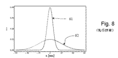
図8において、PSFプロファイルの2つの例が示されている。PSFプロファイル61は5nmの1シグマぼけのものであるのに対して、PSFプロファイル62は、20nmの1シグマぼけのものであり、VSBカラムを通る電流が増すことによってプロファイル62が低下しているのは明らかである。ぼけが無視される(「ゼロぼけ」)場合、図9における、30nmの線幅を有する線の強度プロファイル63が示される。強度プロファイルの「0.5」レベルは、「明瞭にする線量」に相当し、レジスト現像につながる。「0.5」レベルは描画する線のエッジを画定するため、ぼけの影響によって、様々な線量寛容度、ひいては、公称の所望の位置から描画するエッジ位置の偏向が生じる場合がある。左側エッジおよび右側エッジそれぞれの所望の位置64および65には、ゼロぼけの強度プロファイル63が満たされる。5nmの1シグマぼけは、大方の場合、強度プロファイル66はこの条件を依然満たすことができるが、10nm、15nmおよび20nmの1シグマぼけそれぞれの強度プロファイル67、68および69にはますます偏向が生じていく。特に、図9から、および、図9aの拡大細部からわかるように、強度プロファイルの位置(すなわち、「0.5」レベルの交点)は、15nmおよび20nmの1シグマぼけの強度プロファイルによってそれぞれ、所望のエッジ位置64および65(それぞれ、左側エッジおよび右側エッジ)から低下したエッジ位置70および70’へと離れるようにずれていく。このことは、VSB描画機では、露光した線幅はぼけに左右されるが、これは、カラムを通る電流の関数であることを示す。限界寸法(CD)の厳しいターゲット条件を満たすために、VSBツールは、描画中に正しい線量および/またはサイズの補正を誘導する必要がある。
In FIG. 8, two examples of PSF profiles are shown. The
上記のような、本出願人によるMBMWツールといったマルチビーム描画機セットアップは、VSB描画ツールまたは複数のレーザビーム描画機のような他の参照ツールと比較して、大きい重要な利点を有する。 A multi-beam drawing machine setup, such as the MBMW tool by Applicants, as described above, has a great and important advantage over other reference tools such as VSB drawing tools or multiple laser beam drawing machines.
並行して、VSBマスク描画機などの複数のレーザビーム描画機および/または参照ツールを用いる市販用または自社専用マスクショップにおけるMBWタイプのデバイスを使用する時、マスクの描画時間の短縮、および/または、改良したマスクパターン品質の達成を実現する目的で、参照ツールによって描画するやり方によるマスクの実現化のためにも、ユーザは、MBWの使用を所望している。第3の目的は、ツール同士を比較するために、参照描画ツールと比較して同じ品質を有するMBWによってマスクを実現することである。 In parallel, when using MBW type devices in a commercial or in-house mask shop with multiple laser beam writer and / or reference tools such as VSB mask writer, reduce mask drawing time and / or For the purpose of achieving improved mask pattern quality, the user also desires the use of MBW for the realization of masks by the method of drawing with a reference tool. A third objective is to implement masks with MBWs that have the same quality as the reference drawing tools in order to compare the tools with each other.
従って、本発明の目的は、参照ツール、例えば、VSBマスク描画ツールに備えたデータセットをMBWタイプのデバイスに供給する方法、および、MBWタイプのデバイスを所望のタスクを行うことができるように適応させることである。 Therefore, an object of the present invention is a method of supplying a data set provided with a reference tool, for example, a VSB mask drawing tool, to an MBW type device, and an adaptation so that the MBW type device can perform a desired task. Is to let.
特殊な場合、特定の性能の特徴を改変するための、例えば、特定の方向に線幅を変更するための、または、小さな正方形パターンの領域を変更するための、もしくは、特定の線の幅を変更するためのタスクがある時、参照ツールはMBWタイプのツールそのものであってもよい。 In special cases, to modify the characteristics of a particular performance, for example, to change the line width in a particular direction, or to change the area of a small square pattern, or to change the width of a particular line. When there is a task to change, the reference tool may be the MBW type tool itself.
本発明の第1の態様によると、荷電粒子マルチビーム処理装置におけるターゲット上に所望のパターンを露光する露光パターンを計算するための方法が提案される。この場合、本開示の初めに説明したような方法を発端として、当該方法は、以下のステップ:
i)ターゲット上の画像領域上にグラフィカル表示として所望のパターンを与えることであって、前記グラフィカル表示は既定の解像度の幅を有し、当該解像度の幅は通常、前記画像領域内の画素の近接する位置間の公称距離より大きい、所望のパターンを与えることと、
ii)畳み込みカーネルを与えることであって、前記カーネルはグラフィカル表示の要素から画素群へのマッピングを記述し、前記画素群は前記要素の公称位置を中心とする、畳み込みカーネルを与えることと、
iii)畳み込みカーネルによるグラフィカル表示の畳み込みによって、多数の画素上で画定された画素ラスターグラフィックスとして公称露光パターンを算出することであって、前記公称露光パターンはターゲット上に公称線量分布を作成するのに適切であり、当該公称線量分布は所望の強度分布を模倣することができる、または、所望のパターンの等高線を実現するのに役立つ場合がある、公称露光パターンを算出することと、
を含む。
According to the first aspect of the present invention, there is proposed a method for calculating an exposure pattern that exposes a desired pattern on a target in a charged particle multi-beam processing apparatus. In this case, starting with the method described at the beginning of this disclosure, the method may be performed in the following steps:
i) To provide a desired pattern as a graphical display on an image area on a target, the graphical display having a predetermined resolution width, the resolution width usually being close to pixels in the image area. To give the desired pattern, which is greater than the nominal distance between the positions to be
ii) To provide a convolution kernel, the kernel describes a mapping from a graphical display element to a pixel group, and the pixel group provides a convolution kernel centered on the nominal position of the element.
iii) The convolution of the graphical display by the convolution kernel is to calculate the nominal exposure pattern as pixel raster graphics defined on a large number of pixels, the nominal exposure pattern creating a nominal dose distribution on the target. To calculate a nominal exposure pattern, which is suitable for, and the nominal dose distribution can mimic the desired intensity distribution or may help achieve contour lines of the desired pattern.
including.
結果として生成された公称露光パターンは、対応する公称線量値P0を画素ごとに適切に含むことができる。ステップiおよびiiを任意の相対的な時間的順序で行うことができることが分かる。 The resulting nominal exposure pattern can adequately include the corresponding nominal dose value P 0 pixel by pixel. It can be seen that steps i and ii can be performed in any relative temporal order.
本発明によるこの解決策は、上述したeMET/MBMW/PML2装置のうちの1つといった、マルチビーム描画デバイスを用いながら、データ入力として参照ツールデータファイルの使用を可能にする、既知のタイプのマルチビーム描画デバイスをそのデータ経路に対して適応させて、所望の品質のCD(限界寸法)、CDU(CD均一性)、パターン忠実性でパターンを実現する一方で、登録(配置)仕様も満たすアプローチを提示する。また、本発明は、参照ツール、例えば、VSBマスク描画機によって必要とされる処理時間と比較して短縮した時間内で、マルチビーム描画デバイスによって(6インチのマスクまたはシリコンウエハなどの)基板の処理を実現する。 This solution according to the invention is a known type of multi that allows the use of reference tool data files as data inputs while using a multi-beam drawing device, such as one of the eMET / MBMW / PML2 devices described above. An approach that adapts a beam drawing device to its data path to achieve a pattern with the desired quality of CD (limit dimensions), CDU (CD uniformity), and pattern fidelity, while also meeting registration (placement) specifications. To present. The present invention also presents a substrate (such as a 6-inch mask or silicon wafer) by a multi-beam drawing device within a reduced time compared to the processing time required by a reference tool, eg, a VSB mask drawing machine. Realize the processing.
本発明はまた、例えば、計量フィードバックを使用して、マルチビーム描画デバイスによってパターン化されたXおよびY方向のパターンにおいて異なる線幅および/またはスケールを較正することによって、マルチビーム描画デバイスの結果を改善するためにも使用可能である。同様に、本発明のカーネルを使用して、修正されるべき特徴のサイズに関する特定の畳み込みカーネルを使用することによって特定のパターンタイプ、例えば、コンタクトホール(典型的には、正方形又は円形パターン)を向上させることができる。 The present invention also produces results for multi-beam drawing devices by, for example, using metric feedback to calibrate different line widths and / or scales in patterns in the X and Y directions patterned by the multi-beam drawing device. It can also be used to improve. Similarly, using the kernel of the present invention, a particular pattern type, eg, a contact hole (typically a square or circular pattern), can be created by using a particular convolution kernel with respect to the size of the feature to be modified. Can be improved.
本発明の別の態様は、荷電粒子の構造化ビームによってターゲットを露光するための荷電粒子マルチビーム処理装置に関する。当該荷電粒子マルチビーム処理装置は、照明システム、パターン画定デバイス、および、投影光学システムを備える。照明システムは、前記荷電粒子のビームを作り、当該ビームを広範なビームにしてパターン画定デバイスを照らすように構成される。パターン画定デバイスは、照らしているビームの形状を多数のサブビームで構成される構造化ビームするように構成される。投影光学システムは、パターン画定デバイスにおいて画定されたビーム形状の画像をターゲット上に投影することで、ターゲット上の画像領域内に多数の画素を露光するように構成される。パターン画定デバイスは、前記サブビームを形成する複数のブランキングアパーチャで構成されたアパーチャアレイを含む。前記複数のブランキングアパーチャは、ブランキングアパーチャの相互の位置を画定する既定の配列で配列される。各ブランキングアパーチャは、対応する露光間隔中にターゲット上に生成された相当するアパーチャ画像上に、対応するブランキングアパーチャを通って露光する線量値に関して選択的に調節可能である。前記線量値は離散グレースケールから選択された対応する値を利用する。ここで、前記所望のパターンの描画プロセス中、一連の露光間隔が設けられ、各露光間隔で、ブランキングアパーチャによって、ターゲット上への結像が行われるため、相当する複数のアパーチャ画像が生成される。本発明によると、処理装置は、参照描画装置における所望のパターンの描画プロセスを模倣するように構成される。前記参照描画装置は、所望のパターンを、処理装置によって描画可能な公称露光パターンに変換するために本発明の方法を使用して、処理装置によって生成されたアパーチャ画像の公称幅より大きい解像度の幅を有する点広がり関数を有する。 Another aspect of the invention relates to a charged particle multi-beam processing apparatus for exposing a target with a structured beam of charged particles. The charged particle multi-beam processing device includes a lighting system, a pattern defining device, and a projection optical system. The lighting system is configured to create a beam of the charged particles and make the beam a broad beam to illuminate the pattern demarcation device. The pattern demarcation device is configured to make the shape of the illuminating beam a structured beam composed of a large number of subbeams. The projection optical system is configured to expose a large number of pixels within an image region on the target by projecting an image of the beam shape defined by the pattern defining device onto the target. The pattern defining device includes an aperture array composed of a plurality of blanking apertures forming the sub-beam. The plurality of blanking apertures are arranged in a default array that defines the positions of the blanking apertures with each other. Each blanking aperture is selectively adjustable with respect to the dose value exposed through the corresponding blanking aperture on the corresponding aperture image generated on the target during the corresponding exposure interval. The dose value utilizes the corresponding value selected from the discrete grayscale. Here, during the drawing process of the desired pattern, a series of exposure intervals are provided, and at each exposure interval, an image is formed on the target by the blanking aperture, so that a plurality of corresponding aperture images are generated. To. According to the present invention, the processing apparatus is configured to mimic the drawing process of a desired pattern in a reference drawing apparatus. The reference drawing device uses the method of the present invention to convert a desired pattern into a nominal exposure pattern that can be drawn by the processing device, and has a resolution width greater than the nominal width of the aperture image generated by the processing device. Has a point spread function with.
もたらされるパターン特徴の配置のより精細な制御を可能にする、本発明の適切な展開では、描画プロセスによって、相互に重複するアパーチャ画像が生成され、当該アパーチャ画像は、ターゲット上に生成された近接するアパーチャ画像の画素位置間の(1以上の因数o、典型的な場合では整数の因数による)距離の倍数である公称幅を有する。その方法は、
iv)公称露光パターンから、アパーチャ画像の露光による前記描画プロセスによって所望のパターンを露光するのに適切な露光パターンを生成する、
さらなるステップを有する。
In a proper deployment of the invention, which allows finer control over the placement of the resulting pattern features, the drawing process produces overlapping aperture images that are generated on the target in close proximity. It has a nominal width that is a multiple of the distance (one or more factors o, typically an integer factor) between the pixel positions of the aperture image. The method is
iv) From the nominal exposure pattern, generate an exposure pattern suitable for exposing the desired pattern by the drawing process by exposing the aperture image.
It has a further step.
本発明の方法の典型的な応用では、ステップiにおけるグラフィカル表示は、ラスター幅を有する参照ラスター上のラスターグラフィックスであり、前記ラスター幅は解像度の幅として使用される。代替的には、グラフィカル表示はベクターグラフィックスであってよい。当該ベクターグラフィックスは、その後、前記画像領域内の画素の近接する位置間の公称距離より大きいのが好ましいラスター幅を有する参照ラスター上のラスターグラフィックスに変換される。 In a typical application of the method of the invention, the graphical representation in step i is raster graphics on a reference raster having a raster width, the raster width being used as the width of the resolution. Alternatively, the graphical display may be vector graphics. The vector graphics are then converted to raster graphics on a reference raster having a raster width that is preferably greater than the nominal distance between adjacent positions of pixels in the image area.
本発明の適切な態様によると、ステップiiiの算出および(存在する場合)後続する算出は、リアルタイムで描画プロセス中に行われ、算出されるデータを永続的に記憶することなく、関連する算出を一時的に行う。 According to a suitable aspect of the invention, the calculation of step iii and the subsequent calculations (if any) are performed in real time during the drawing process to perform the relevant calculations without permanently storing the calculated data. Do it temporarily.
1つの有利な実現において、畳み込みカーネルは、前記処理装置によって模倣される参照描画装置の点広がり関数を表すことができる。典型的には、当該処理装置自体の点広がり関数は、この文脈において、参照描画装置よりもかなり小さいため、無視できるものであることが多い。 In one advantageous implementation, the convolution kernel can represent the point spread function of the reference drawing device mimicked by said processing device. Typically, the point spread function of the processing device itself is much smaller than the reference drawing device in this context and is often negligible.
畳み込みカーネルの1つの適切な表示は、画素値の離散マトリックスの形のものである。よって、ステップiiiの畳み込みを、離散畳み込みとして、すなわち、マトリックスの離散要素上で行うことができる。 One good representation of a convolution kernel is in the form of a discrete matrix of pixel values. Therefore, the convolution of step iii can be performed as a discrete convolution, i.e., on the discrete elements of the matrix.
本発明の別の態様によって、画像領域上の2つの主な方向に関して異方性を有する畳み込みカーネルが実現される。これによって、参照ツールのかかる異方性の性質を模倣するおよび/または補償するために、楕円形の点広がり関数または他の異方性を適切に扱うことができる。1つの有利な応用として、カーネルの異方性を使用して、模倣されるマルチビーム描画機および/または参照ツールに関して、ブランキングアパーチャによるターゲット上への結像の異方性を補償することができる。 Another aspect of the invention provides a convolutional kernel that has anisotropy with respect to two major orientations on the image region. This allows the elliptical point spread function or other anisotropy to be adequately handled in order to mimic and / or compensate for such anisotropy properties of the reference tool. One advantageous application is to use the anisotropy of the kernel to compensate for the anisotropy of the image formation on the target by the blanking aperture for the mimicked multi-beam writer and / or reference tool. it can.
さらには、畳み込みカーネルは、時間依存値、すなわち、模倣される参照描画装置の時間依存の描画性質に相応する時間依存性を含むこともできる。例えば、時間依存値は、ターゲット上に存在する荷電粒子ビーム感応レジスト層といった、ターゲットの感応性のエージング関数に相当する時間依存性を含むことができる。さらなる例として、代替的にはまたは組み合わせて、粒子ビームが時間によって変動する場合がある粒子電流の生成する光源から生成される場合、時間依存性は、該光源から放出される全電流のゆらぎ関数に相当する関数を含むことができる。 Furthermore, the convolution kernel can also include a time-dependent value, i.e., a time dependency corresponding to the time-dependent drawing property of the mimicked reference drawing device. For example, the time-dependent value can include a time dependence corresponding to the aging function of the target's sensitivity, such as a charged particle beam sensitive resist layer existing on the target. As a further example, if the particle beam, alternative or in combination, is generated from a light source that produces a particle current that may fluctuate over time, the time dependence is a fluctuation function of the total current emitted from that light source. Can include a function corresponding to.
本発明の別の有利な展開では、2つ以上の畳み込みカーネルを用いる。例えば、各カーネルは、画像領域内の複数のサブ領域の中の対応するサブ領域上で使用可能である。その対応するサブ領域は、画像フィールドにわたる点広がり関数における差異を考慮するために有用である場合がある(例えば、ぼけは画像フィールドにわたって変動する場合がある)。また、複数のアパーチャアレイがパターン画定デバイスにおいて存在し、描画プロセスの様々な段階で使用され、その後、各アパーチャアレイに対して、関連のカーネルを使用することが可能である。 Another advantageous development of the present invention uses two or more convolution kernels. For example, each kernel can be used on the corresponding sub-region within a plurality of sub-regions within the image region. The corresponding sub-region may be useful to account for differences in the point spread function across the image field (eg, blur may vary across the image field). It is also possible that multiple aperture arrays exist in the pattern defining device and are used at various stages of the drawing process, after which the associated kernel can be used for each aperture array.
有利には、グレースケールデータといった、実際の描画プロセスにおいて使用されるデータよりも高いデータ精度で算出を行うことができる。この場合、ステップiiiにおける畳み込みを、離散グレースケールの解像度よりも高い演算精度を有する演算値を使用して行うことができる。 Advantageously, the calculation can be performed with higher data accuracy than the data used in the actual drawing process, such as grayscale data. In this case, the convolution in step iii can be performed using an arithmetic value having an arithmetic accuracy higher than the resolution of the discrete grayscale.
また、グラフィカル表示の解像度の幅は、荷電粒子マルチビーム処理装置によって生成されたアパーチャ画像の公称幅より大きいものであってよい。さらに、本発明の基礎となる描画プロセスの好ましい実現では、アパーチャ画像の位置は、露光間隔中、画素の位置においてターゲットに対して固定されたままであるが、露光間隔同士の間では、アパーチャ画像の位置はターゲット上でずれるため、ターゲット上の前記画像領域内の多数の画素を露光する。 Also, the resolution width of the graphical display may be greater than the nominal width of the aperture image generated by the charged particle multi-beam processor. Further, in a preferred implementation of the drawing process underlying the present invention, the position of the aperture image remains fixed with respect to the target at the pixel position during the exposure interval, but between the exposure intervals of the aperture image. Since the position shifts on the target, a large number of pixels in the image area on the target are exposed.
以下では、図面を参照して本発明をより詳細に説明する。 Hereinafter, the present invention will be described in more detail with reference to the drawings.
以下では、次で概略的に示されるような図面を参照して、本発明をより詳細に説明する。 Hereinafter, the present invention will be described in more detail with reference to the drawings schematically shown below.
後述される本発明の実施形態は、基本的には既知のタイプであるが、後述されるように、本発明を収容するように適切に修正された、本出願人によるマルチビーム露光ツールのオン線のデータ経路において使用される、「畳み込みカーネルに適合する参照ツールに対するマルチビーム描画機」、略してMRMCカーネル、または、簡単に言えば「カーネル」を実装する。本発明は、以下で論じられる実施形態に制限されず、当該実施形態は本発明の適切な実装形態を表すに過ぎないことは理解すべきである。 Embodiments of the invention described below are of essentially known types, but as described below, the Applicant turns on a multi-beam exposure tool that has been appropriately modified to accommodate the invention. Implements a "multi-beam drawing machine for reference tools that fits the convolution kernel" used in the line data path, the MRMC kernel for short, or simply the "kernel". It should be understood that the invention is not limited to the embodiments discussed below, and that embodiment merely represents a suitable implementation of the invention.
リソグラフィ装置
本発明の好ましい実施形態を用いるのに適切なリソグラフィ装置の全体像を図1に示す。下記では、本発明の開示に必要とされるその細部のみを示し、明確にするために、図1の範囲に示さない構成要素もある。リソグラフィ装置1の主要構成要素は、本例では、図1において垂直方向に下行するリソグラフィビームlb、pbの方向に相当して、照明システム3、パターン画定(PD)システム4、投影システム5、および、基板16を有するターゲットステーション6である。装置1全体は、荷電粒子のビームlb、pbが当該装置の光軸cwに沿って妨げられずに確実に伝達されるように、高真空で保持された真空ハウジング2に収められている。荷電粒子光学システム3、5は、静電レンズおよび/または磁気レンズを使用して実現される。
Lithography Equipment A complete picture of a lithography equipment suitable for using the preferred embodiments of the present invention is shown in FIG. In the following, for the sake of showing and clarifying only the details required for the disclosure of the present invention, some components are not shown in the scope of FIG. In this example, the main components of the
照明システム3は、例えば、電子銃7、抽出システム8、および、集光レンズシステム9を備える。しかしながら、電子の代わりに、一般に他の荷電粒子も使用することができる。電子は別として、これらを、例えば、水素イオンもしくはより重いイオン、荷電した原子集団、または、荷電分子とすることができる。
The
抽出システム8は、粒子を、典型的には数keV、例えば、5keVの定められたエネルギーへと加速させる。集光レンズシステム9によって、光源7から放出された粒子は、リソグラフィビームlbとして機能する、幅広く、実質的にテレセントリックな粒子ビーム50に形成される。リソグラフィビームlbは、次いで、複数の開口部(アパーチャとも言う)を有する複数のプレートを備えるPDシステム4を照らす。PDシステム4は、リソグラフィビームlbの経路における特定の位置で保持されるため、複数のアパーチャおよび/または開口部を照らし、複数のビームレットに分裂する。
The
アパーチャ/開口部の一部は、「スイッチを入れる」または「開放される」ことで、該アパーチャ/開口部の一部から伝導されるビームの部分を可能にし、すなわち、ビームレット51がターゲットに到達できるという意味で、入射ビームには透明とされ、他のアパーチャ/開口部は「スイッチが切られる」または「閉鎖され」、すなわち、相当するビームレット52はターゲットに到達できないため、実際上、これらのアパーチャ/開口部はビームに対する透明性がない(不透明である)。よって、リソグラフィビームlbは構造化されて、PDシステム4から出現するパターンビームpbになる。スイッチを入れたアパーチャのパターン、リソグラフィビームlbには透明なPDシステム4の一部のみが、荷電粒子感応レジスト17によって覆われた基板16上で露光されるパターンに従って選択される。アパーチャ/開口部の「スイッチを入れる/切る」ことは、通常、PDシステム4のプレートのうちの1つに設けられた適切なタイプの偏向手段によって実現される。「スイッチを切られた」ビームレット52は、(十分ではあるが非常に小さい角度で)その経路から偏向するため、ターゲットに到達することができず、リソグラフィ装置において、例えば、吸収プレート11のある場所で単に吸収される。
A portion of the aperture / opening is "switched on" or "opened" to allow a portion of the beam to be conducted from the portion of the aperture / opening, i.e. the
次いで、パターンビームpbによって表されるパターンは、電気―磁気―光学投影システム5によって基板16上に投影され、ここでビームによって「スイッチを入れられた」アパーチャおよび/または開口部の画像が形成される。投影システム5は、2つのクロスオーバーc1およびc2により例えば200:1の縮小を実行する。基板16は、例えば、粒子感応レジスト層17で覆われた6インチのマスクブランクまたはシリコンウエハである。基板は、チャック15によって保持され、かつ、ターゲットステーション6の基板ステージ14によって位置付けられる。
The pattern represented by the pattern beam pb is then projected onto the
露光されるパターンに関する情報は、電子パターン情報処理システム18によって実現されるデータ経路によって、PDシステム4に供給される。データ経路については、「データ経路」のセクションにおいてさらに以下で説明する。
Information about the pattern to be exposed is supplied to the
図1に示される実施形態では、投影システム5は、複数の連続する電気−磁気−光学投影機ステージ10a、10b、10cで構成される。投影機10a、10b、10cは、静電レンズおよび/または磁気レンズ、ならびに、場合により他の偏向手段を含むことが好ましい。これらのレンズおよび手段は、それらの応用が従来技術において周知であるため、符号の形のみで示される。投影システム5は、クロスオーバーc1、c2を通して縮小結像を用いている。両ステージのための縮小因数は、数百の結果の全体的な縮小が、例えば200:1の縮率となるように選択される。この程度の縮小は、PDデバイスの小型化の問題を軽減するために、リソグラフィセットアップによって特に適切である。
In the embodiment shown in FIG. 1, the
投影システム5全体では、レンズおよび/または偏向手段が、色収差および幾何学収差に関して広範囲にわたって補償されるようにする。全体として横方向に、すなわち、光軸cwに対して直角を成す方向に沿って画像をずらす手段として、偏向手段12a、12b、および、12cは集光器3および投影システム5に設けられる。偏向手段は、例えば、多重極電極システムとして実現可能である。当該多重極電極システムは、図1におけるステージ偏向手段12cの場合のように、光源抽出システム12aの近くに、もしくは、偏向手段12bと共に図1に示されるようにクロスオーバーのうちの1つの近くに、または、対応する投影機の最終レンズ10cの後のいずれかに位置付けられる。この装置において、多重極電極の配列が、偏向手段としてステージ動作との関連で画像をずらすために、かつ、荷電光学アライメントシステムと連動する結像システムの補正のために使用される。これらの偏向手段10a、10b、10cは、停止プレート11と連動するPDシステム4の偏向アレイ手段がパターンビームpdの選択されたビームレットのスイッチを「入れる」または「切る」ために使用されるため、該偏向アレイ手段と混同されることがないが、偏向手段10a、10b、10cは、全体として粒子ビームにのみ対処する。軸方向の磁場を設けるソレノイド13を使用してプログラム可能なビームの集団を回転させることも可能である。
Throughout the
図2の部分的な詳細は、PDシステム4の1つの適切な実施形態を示す。PDシステム4は、連続した構成で積み重ねられた3つのプレート:「アパーチャアレイプレート」(AAP)20、「偏向アレイプレート」(DAP)30、および、「磁場境界アレイプレート」(FAP)40を備える。「プレート」と言う用語は、対応するデバイスの全体的な形状に言及するが、単一のプレート構成要素が通常、好ましい実装様式であるとしても、プレートが単一のプレート構成要素として実現されると、必ずしも示しているわけではない。なおかつ、ある実施形態では、アパーチャアレイプレートなどの「プレート」は、複数のサブプレートで構成されてよい。当該プレートは、Z方向(図2の垂直軸)に沿った相互間の距離で、互いに平行に配列されるのが好ましい。
Partial details of FIG. 2 show one suitable embodiment of
AAP20の平坦な上面は、荷電粒子集光器光学部品/照明システム3に対する定められた電位界面を形成する。AAPを、例えば、薄い中央部分22を有する(およそ1mmの厚さの)シリコンウエハの正方形または矩形片から作ることができる。プレートは、導電性保護層23によって覆われてよい。導電性保護層23は、水素イオンまたはヘリウムイオン(特許文献2の一節)を使用する時に特に有利となる。電子または重イオン(例えば、アルゴンまたはキセノン)を使用する時、21および22それぞれの表面部分によってもたらされた層23はシリコンから作られてもよく、それによって、層23とバルク部分21、22との間に界面はない。
The flat top surface of the
AAP20は、薄くなった部分22を横断する開口部によって形成された複数のアパーチャ24を備える。アパーチャ24は、薄くなった部分22に設けられたアパーチャ領域内に既定の配列で配列されることで、アパーチャアレイ26を形成する。アパーチャアレイ26におけるアパーチャの配列は、例えば、千鳥配列、または、規則的な矩形もしくは正方形アレイ(図4を参照)であってよい。示される実施形態では、アパーチャ24は、層23に加工された直線プロファイルと、開口部の下方出口25がアパーチャ24の主要部分よりも広くなるようにした、AAP20のバルク層における「逆行」プロファイルとを有するように実現される。直線プロファイルおよび逆行プロファイルは両方とも、反応性イオンエッチングといった現状技術の構造化技法によって加工可能である。逆行プロファイルは、開口部を通過するビームの反射鏡電荷効果を大きく低減させる。
The
DAP30は、複数の開口部33を備えたプレートである。開口部33の位置は、AAP20におけるアパーチャ24の位置に相当し、開口部33には、開口部33をその対応する経路から選択的に通過する個々のビームレットを偏向するように構成された電極35、38が設けられている。DAP30は、例えば、ASIC回路構成を有するCMOSウエハの後処理を行うことによって加工可能である。DAP30は、例えば、正方形または矩形の形状を有する1片のCMOSウエハで作られ、薄くされている(が、22の厚さと比較すると適切に厚くなっている場合がある)中央部分32を保持するフレームを形成する肉厚部分31を含む。中央部分32におけるアパーチャ開口部33は、24と比較して(例えば、各側部でおよそ2μmずつ)広くなっている。CMOS電子機器34を設けて、MEMS技法によってもたらされる電極35、38を制御する。各開口部33に隣接して、「接地」電極35および偏向電極38が設けられる。共通の接地電位に接続された接地電極35は、電気的に相互接続され、荷電を防ぐための逆行部分36と、CMOS回路構成に対する不必要なショートカットを防止するための絶縁部分37とを含む。接地電極35は、シリコンバルク部31および32と同じ電位のCMOS回路構成34の接地電極部品に接続されてもよい。
The
偏向電極38は、静電位が選択的に印加されるように構成され、かかる静電位が電極38に印加されると、これによって、公称経路から偏向させるような、相当するビームレットに対する偏向を引き起こす電界が生成されることになる。電極38は、同様に、荷電を回避するために逆行部分39を有することができる。電極38のそれぞれは、その低部分において、CMOS回路構成34内で対応する接触部位に接続される。
The deflection electrode 38 is configured such that an electrostatic potential is selectively applied, which when applied to the electrode 38 causes deflection for the corresponding beamlet, such as deflecting from the nominal path. An electric potential will be generated. The electrode 38 can also have a
接地電極35の高さは、ビームレット間のクロストーク効果を抑制するために、偏向電極38の高さより高い。 The height of the ground electrode 35 is higher than the height of the deflection electrode 38 in order to suppress the crosstalk effect between the beamlets.
図2に示されるDAP30を有するPDシステム4の配列は、いくつかの可能性のうちの1つに過ぎない。(図示されない)変形では、DAPの接地電極35および偏向電極38を、下流ではなく(上方に向けられた)上流に指向させることができる。さらに、例えば、接地電極および偏向電極が埋め込まれたDAP構成は、当業者によって考案可能である(特許文献3など、本出願人名義の他の特許を参照)。
The sequence of
FAPとして機能する第3のプレート40は、下流で縮小する荷電粒子投影光学部品5の第1のレンズ部品に面する平面を有するため、画定された電位界面を投影光学部品の第1のレンズ10aにもたらす。FAP40の肉厚部分41は、薄くした中央部分42と共に、シリコンウエハの一部から作られた正方形または矩形フレームである。FAP40は、AAP20およびDAP30の開口部24、33に相当するが、それらと比較して広幅の複数の開口部43を備える。
Since the
PDシステム4、特にその第1のプレート、AAP20は、幅広の荷電粒子ビーム50(本明細書において、「幅広の」ビームは、AAPにおいて形成されたアパーチャアレイの全領域を覆うためにビームが十分広幅であることを意味する)によって照らされ、それによって、アパーチャ24から伝導される時、何千ものマイクロメートルサイズのビームレット51に分割される。ビームレット51は、妨げられずにDAPおよびFAPを横断することになる。
The
既に述べたように、偏向電極38がCMOS電子機器によって電力供給される時はいつでも、偏向電極と、相当する接地電極との間に電界が生成されることになり、それによって、対応するビームレット52が通過する際に小さいが十分な偏向がもたらされる(図2)。偏向したビームレットは、開口部33および43それぞれが十分広幅に作られているため、妨げられずにDAPおよびFAPを横断することができる。しかしながら、偏向ビームレット52は、サブカラムの停止プレート11においてフィルターを通して除去される(図1)。よって、DAPによる影響を受けないビームレットのみが基板に到達することになる。
As already mentioned, whenever the deflection electrode 38 is powered by a CMOS electronics, an electric field will be generated between the deflection electrode and the corresponding ground electrode, thereby the corresponding beamlet. A small but sufficient deflection is provided as the 52 passes (Fig. 2). The deflected beamlet can traverse the DAP and FAP unimpeded because the
縮小荷電粒子光学部品5の縮小因数は、ビームレット、およびPDデバイス4におけるそれらビームレットの相互間の距離の寸法、ならびに、ターゲットにおける構造体の所望の寸法を考慮して適切に選択される。これによって、PDシステムにおけるマイクロメートルサイズのビームレットが可能になり、ナノメートルサイズのビームレットが基板上に投影される。
The reduction factor of the reduction charged
AAPによって形成される(影響を受けていない)ビームレット51の集合体は、投影荷電粒子光学部品の所定の縮小因数Rによって基板に投影される。よって、基板において、幅BX=AX/RおよびBY=AY/Rそれぞれを有する「ビームアレイフィールド」(BAF)が投影される。式中、AXおよびAYは、X方向およびY方向それぞれに沿ったアパーチャアレイフィールドのサイズを示す。基板におけるビームレット(すなわち、アパーチャ画像)の公称幅は、bX=aX/RおよびbY=aY/Rそれぞれによって示される。式中、aXおよびaYは、DAP30のレベルにおいて、X方向およびY方向それぞれに沿って測定されるビームレット51のサイズを示す。
The aggregate of
図2に描写された個々のビームレット51、52が、2次元のX−Yアレイにおいて配列されたかなり多くの、典型的には何千ものビームレットを表すことに留意することは、意味のあることである。本出願人は、例えば、イオン、および、何千もの(例えば、262,144の)プログラム可能なビームレットを有する電子マルチビームカラムについてR=200の縮小因数によるマルチビーム荷電粒子光学部品を実現している。本出願人は、基板においておよそ82μm×82μmのビームアレイフィールドを有するようなカラムを実現している。これらの例は、例示の目的で述べられ、限定的な例として解釈されないものとする。
It is meaningful to note that the
図3を参照すると、PDシステム4によって画定されるパターン画像pmがターゲット16上に作られている。荷電粒子感応レジスト層17によって覆われたターゲット表面は、露光する1つまたは複数の領域r1を含むことになる。一般的に、ターゲット上に露光したパターン画像pmは、通常は、パターン化される領域r1の幅より十分小さい有限サイズy0を有する。従って、走査式ストライプ露光法が活用される。この場合、ターゲットは、入射ビーム下に移されることで、ターゲット上のビームの位置を永続的に変更し、ビームはターゲット表面上で効果的に走査される。本発明の目的として、ターゲット上のパターン画像pmの相対運動のみが妥当であることを強調する。相対移動によって、パターン画像pmを、幅y0の一連のストライプs1、s2、s3、・・・sn(露光ストライプ)を形成するように、領域r1上を移動させる。ストライプ一式は基板表面の全領域を覆う。走査方向sdは、ストライプ間で均一であるか一つおきであってよい。
Referring to FIG. 3, a pattern image pm defined by the
図5は、10×16=180画素のサイズの結像パターンの簡単な例を示す。ここで、露光領域のいくつかの画素p100を100%のグレーレベル401まで露光し、他の画素p50を完全グレーレベルの50%だけ露光する402。残りの画素を0%線量に露光する403(全く露光されない)。当然ながら、本発明の現実的な応用では、標準画像の画素数はもっと高いものになる。しかしながら、図5において、画素数は、いっそう明確にするために180のみとなっている。また、一般に、さらに高いグレーレベルを、0%から100%までのスケール内で使用することになる。 FIG. 5 shows a simple example of an imaging pattern having a size of 10 × 16 = 180 pixels. Here, 402, some pixels p100 in the exposure region are exposed to 100% gray level 401, and other pixels p50 are exposed by 50% of the complete gray level. 403 exposing the remaining pixels to 0% dose (not exposed at all). Of course, in a practical application of the present invention, the number of pixels of a standard image will be higher. However, in FIG. 5, the number of pixels is only 180 for further clarity. Also, higher gray levels will generally be used within the scale from 0% to 100%.
よって、パターン画像pm(図3)は、複数のパターン画素pxで構成され、当該パターン画素pxは、露光される所望のパターンに従った線量値で露光される。しかしながら、有限数のアパーチャのみがPDシステムのアパーチャフィールドにおいて存在するため、画素pxのサブセットのみを同時に露光することができることは理解されるべきである。スイッチを入れたアパーチャのパターンは、基板上に露光されるパターンに従って選択される。よって、実際のパターンにおいて、十分な線量で全ての画素が露光されるわけではないが、いくつかの画素は実際のパターンに従って「スイッチを切られる」ことになり、任意の画素(または、同等に、画素を覆うビームレットごとに)、ターゲット上に露光または構造化されるパターンに応じて、画素の「スイッチを入れる」か「スイッチを切る」かに関わらず、画素露光サイクル間で露光線量を可変とすることができる。 Therefore, the pattern image pm (FIG. 3) is composed of a plurality of pattern pixels px, and the pattern pixels px are exposed at a dose value according to a desired pattern to be exposed. However, it should be understood that only a subset of pixels px can be exposed at the same time, since only a finite number of apertures are present in the aperture field of the PD system. The pattern of the switched on aperture is selected according to the pattern exposed on the substrate. Thus, in the actual pattern, not all pixels are exposed at a sufficient dose, but some pixels will be "switched off" according to the actual pattern and any pixel (or equivalent). Depending on the pattern exposed or structured on the target (for each beamlet covering the pixel), the exposure dose between pixel exposure cycles, whether the pixel is "switched on" or "switched off". It can be variable.
基板16を連続して移動させる間、ターゲット上のパターン画素pxに相当する同じ画像要素を、一連のアパーチャの画像によって何度も覆うことができる。同時に、PDシステムにおけるパターンは、PDシステムのアパーチャから少しずつずらされる。よって、ターゲット上のある場所の1画素を考慮すると、アパーチャ全てがその画素を覆う時にスイッチが入れられる場合、これによって、最高露光線量レベル:100%に相当する「白」の色調が生じることになる。「白」の色調に加えて、最低(「黒」)露光線量レベルと最高(「白」)露光線量レベルとの間に補間することになる、より低い線量レベル(「グレーの色調」とも呼ばれる)に従って、ターゲットにおける画素を露光することができる。グレーの色調は、例えば、1画素の描画に関わる場合があるアパーチャのサブセットのみのスイッチを入れることによって実現可能であり、例えば、16個のアパーチャのうち4つは25%のグレーレベルを示すことになる。別のアプローチは、関わるアパーチャのアンブランキング露光の継続期間を低減させることである。よって、1つのアパーチャ画像の露光継続期間は、グレースケールコード、例えば、整数によって制御される。露光したアパーチャ画像は、ゼロ、ならびに、最高露光継続期間および線量レベルに相当する一定数のグレーの色調のうち1つの明示である。グレースケールは通常、グレー値のセット、例えば、0、1/(ny−1)&、i/(ny−1)、&、1を定義する。ここで、nyはグレー値の数で、iは整数(「グレー指数」、0≦i≦ny)である。しかしながら、一般的に、グレー値は、等距離である必要はなく、0と1との間の非減少数列を形成する。
While the
図5は、基本的なレイアウトによる、PDデバイスのアパーチャフィールドにおけるアパーチャの配列を示し、また、以下で使用されるいくつかの量および略語を示す。濃い色調で示された、ターゲット上に投影されるアパーチャ画像b1の配列が示されている。主軸XおよびYは、ターゲット運動の進行方向(走査方向sd)、および、鉛直方向にそれぞれ相当する。各アパーチャ画像は、方向XおよびYそれぞれに沿った幅bXおよびbYを有する。アパーチャは、それぞれNXおよびNYとなる行および列において近接するアパーチャ間のオフセットで、それぞれMXおよびMYアパーチャを有する行および列に沿って配列される。結果として、各アパーチャ画像には、NX・bX・NY・bYの領域を有する概念上のセルC1が属し、アパーチャ配列は、矩形になるように配列されたMX・MYセルを含有する。以下では、これらのセルC1を「露光セル」と言う。ターゲット上に投影される完全なアパーチャ配列は、BX=MX・NX・bX、BY=MY・NY・bYの寸法を有する。以降の論述では、一般性を何ら制限することなくさらなる説明を全て行うために、矩形グリッドの特殊な場合として正方形グリッドを前提とし、b=bX=bY、M=MX=MY、および、N=NX=NYであり、ここでMは整数とする。よって、「露光セル」はターゲット基板上でN・b×N・bのサイズを有する。 FIG. 5 shows an array of apertures in the aperture field of a PD device with a basic layout and also shows some quantities and abbreviations used below. An array of aperture images b1 projected onto the target, shown in dark tones, is shown. The spindles X and Y correspond to the traveling direction of the target motion (scanning direction sd) and the vertical direction, respectively. Each aperture image has widths bX and bY along directions X and Y, respectively. Apertures are arranged along rows and columns with MX and MY apertures, respectively, at offsets between adjacent apertures in rows and columns that are NX and NY, respectively. As a result, each aperture image belongs to a conceptual cell C1 having a region of NX, bX, NY, bY, and the aperture array contains MX, MY cells arranged in a rectangular shape. Hereinafter, these cells C1 will be referred to as “exposure cells”. The complete aperture array projected onto the target has dimensions of BX = MX · NX · bX, BY = MY · NY · bY. In the following discussion, in order to give all further explanations without limiting generality, we assume a square grid as a special case of a rectangular grid, b = bX = bY, M = MX = MY, and N = NX = NY, where M is an integer. Therefore, the "exposure cell" has a size of N · b × N · b on the target substrate.
2つの近接する露光位置間の距離は、以下ではeと表示される。一般に、距離eを、アパーチャ画像の公称幅bと異ならせることができる。もっとも単純な場合では、b=eであり、これは、2×2露光セルC3の配列例として図6aに示されており、1つのアパーチャ画像bi0は1画素(の公称位置)を覆う。図6bに示される(ならびに、特許文献4および特許文献5の教示に沿った)別の興味深い例では、eはアパーチャ画像の幅bの分数b/oであってよく、ここで、o>1であり、これは、オーバーサンプリング因数とも言う整数であるのが好ましい(が必ずしもそうではない)。この場合、アパーチャ画像は、種々の露光の過程で空間的に重なり合い、それによって、パターンの配置のより高い解像度を展開することが可能になる。その後、アパーチャの各画像は、複数の画素、すなわち、o2画素を一度に覆うようになる。ターゲットに結像されるアパーチャフィールドの全領域は、(NMo)2画素を含むことになる。アパーチャ画像の配置の観点からすれば、このオーバーサンプリングは、ターゲット領域を単に覆うのに必要になるものと(空間的配置においてより優れているため)異なるいわゆる配置グリッドに相当する。
The distance between two adjacent exposure positions is represented below as e. In general, the distance e can be different from the nominal width b of the aperture image. In the simplest case, b = e, which is shown in FIG. 6a as an array example of the 2 × 2 exposed cell C3, where one aperture image bi0 covers (nominal position) one pixel. In another interesting example shown in FIG. 6b (and in line with the teachings of
図6bは、配置グリッドと組み合わせたo=2のオーバーサンプリング、すなわち、パラメータo=2、N=2を有する露光セルC4によるアパーチャアレイの画像の一例を示す。よって、各公称場所(図6bにおける小正方形フィールド)上に、4つのアパーチャ画像bi1(破線)が印刷され、これは、X方向およびY方向双方においてピッチeごとの規則的なグリッド上のオフセットである。静止したアパーチャ画像のサイズは同じ値bであるが、配置グリッドのピッチeはここでb/o=b/2となる。前回の公称場所に対するオフセット(配置グリッドのオフセット)もb/2のサイズである。同時に、各画素の線量および/またはグレーの色調は、対応する画素を覆うアパーチャ画像にとって適切なグレー値を選択することによって、適応(低減)可能である。その結果、サイズaの領域は印刷されるが、より精細な配置グリッドによって、配置精密度が向上する。図6bと図6aとを直接比較することによって、アパーチャ画像の場所が、正に、以前よりも2倍(一般的に、o倍)精細な配置グリッド上に配列され、アパーチャ画像そのものが重ね合わされる。ここで、露光セルC4は、描画プロセス中に扱われる(No)2の場所(すなわち、「画素」)、例えば、o2の因数ごとに、以前よりも多い画素を含有する。それに応じて、アパーチャ画像のサイズがb×bの領域bi1は、図6Bにおいてo=2であるオーバーサンプリング(「二重グリッド」とも呼ばれる)の場合、o2=4画素に関連付けられる。当然ながら、oはまた、任意の他の整数値、特に4(「四重グリッド」、図示せず)もしくは8、または、2=1.414といった1より大きい非整数値も取ることができる。 FIG. 6b shows an example of an image of the aperture array by the exposure cell C4 having o = 2 oversampling combined with the arrangement grid, i.e., parameters o = 2, N = 2. Thus, four aperture images bi1 (dashed lines) are printed on each nominal location (small square field in FIG. 6b), with regular grid offsets for each pitch e in both the X and Y directions. is there. The size of the stationary aperture image is the same value b, but the pitch e of the arrangement grid is b / o = b / 2 here. The offset with respect to the previous nominal location (offset of the placement grid) is also b / 2 size. At the same time, the dose and / or gray tones of each pixel can be adapted (reduced) by selecting the appropriate gray value for the aperture image covering the corresponding pixel. As a result, the area of size a is printed, but the finer placement grid improves placement accuracy. By directly comparing FIG. 6b and FIG. 6a, the locations of the aperture images are arranged exactly on an arrangement grid that is twice (generally o times) finer than before, and the aperture images themselves are superimposed. To. Here, the exposure cell C4 contains more pixels than before for each of the (No) 2 locations (ie, "pixels") treated during the drawing process, eg, o 2. Correspondingly, the region bi1 in which the size of the aperture image is b × b is associated with o 2 = 4 pixels in the case of oversampling (also referred to as “double grid”) where o = 2 in FIG. 6B. Of course, o can also take any other integer value, in particular a non-integer value greater than 1 such as 4 (“quadruple grid”, not shown) or 8, or 2 = 1.414.
図7は、本発明に適切な画素の露光体系を示す。一連のフレームが示されており、ここでは、上(より早い)から下(より遅い)へと時間は増えている。本図におけるパラメータ値はo=1、N=2であり、また、矩形のビームアレイではMX=8およびMY=6を前提とする。ターゲットは左へ連続して移動するのに対し、ビーム偏向は、本図の左側に示されるシーソー関数によって制御される。長さT1の各時間間隔中に、ビーム画像は、(「配置グリッド」の位置に相当する)ターゲット上の位置において固定されたままである。よって、ビーム画像は、配置グリッドシーケンスp11、p21、p31を通り抜けるように示される。配置グリッドの1サイクルを、ターゲット運動vによって時間間隔L/v=NMb/v内で露光する。各配置グリッドにおける露光の時間T1は、「露光長」と呼ぶ、長さLG=vT1=L/(No)2=bM/No2に相当する。
FIG. 7 shows a pixel exposure system suitable for the present invention. A series of frames is shown, where the time is increasing from top (earlier) to bottom (slower). The parameter values in this figure are o = 1 and N = 2, and it is assumed that MX = 8 and MY = 6 in the rectangular beam array. The target moves continuously to the left, while the beam deflection is controlled by the seesaw function shown on the left side of this figure. During each time interval of length T1, the beam image remains fixed at a position on the target (corresponding to the position of the "placement grid"). Thus, the beam image is shown to pass through the placement grid sequences p11, p21, p31. One cycle of the placement grid is exposed by the target motion v within the time interval L / v = NMb / v. Time T1 of exposure in each placement grid, referred to as "exposure length" corresponding to the length L G = vT1 = L / ( No) 2 = bM /
ビームレットを、ターゲットと共に1セットの画像要素の露光中に、LGの距離にわたって移動させる。換言すると、全てのビームレットは、時間間隔T1中、基板の表面に対して固定された位置を維持する。距離LGに沿ってターゲットと共にビームレットを移動させた後、ビームレットを(非常に短い時間内で)即座に再配置して、次の配置グリッドの画像要素の露光を開始する。配置グリッドサイクルの位置p11・・・p31を通した全サイクル後、X方向(走査方向)に平行であるさらなる縦方向オフセットL=bNMによって、シーケンスが新たに開始される。ストライプの開始および終了時に、露光方法は、連続的な被覆をもたらさなくてもよいため、完全に充填しない長さLの余地があってよい。 Beamlet, during the exposure of the image elements of one set with the target, it is moved over a distance of L G. In other words, all beamlets maintain a fixed position with respect to the surface of the substrate during the time interval T1. After distance along the L G to move the beamlets with the target, and realign the beamlets (within a very short time) in real exposure is started in the image elements of the next placement grid. After all cycles through positions p11 ... p31 of the placement grid cycle, a new sequence is started with a further vertical offset L = bNM parallel to the X direction (scanning direction). At the beginning and end of the stripes, the exposure method does not have to result in a continuous coating, so there may be room for a length L that is not completely filled.
例えば、VSBマスク描画ツールといった、参照描画ツールとは対照的に、本発明の始点であるMBWセットアップは、同じスポットサイズ、例えば、20nm×20nmを均一に使用する。さらに、スポット間の重複部分を、選択された重複量で使用することができる。「二重グリッド」マルチビーム露光において、スポット間の重複部分は、X方向およびY方向におけるビームサイズの半分である。「四重グリッド」マルチビーム露光では、スポット間の重複部分は、X方向およびY方向におけるビームサイズの1/4である。ターゲット上に形成された単一のアパーチャ画像のサイズはaX/Rである。式中、aXはアパーチャアレイプレート(AAP)におけるアパーチャの開口幅であり、Rは荷電粒子投影光学部品の縮小因数である。各スポットは離散的な線量レベルで露光される。例えば、線量レベルをプログラミングするために4ビット使用する時、各スポットの線量レベルは、0、1、2、・・・14、または、15ユニットとなるように選択可能であり、ここで、15ユニットは100%の最高線量レベルを表している。 In contrast to reference drawing tools, such as the VSB mask drawing tool, the MBW setup, which is the starting point of the present invention, uniformly uses the same spot size, eg, 20 nm x 20 nm. In addition, the overlap between spots can be used with the selected amount of overlap. In a "double grid" multi-beam exposure, the overlap between the spots is half the beam size in the X and Y directions. In a "quadruple grid" multi-beam exposure, the overlap between the spots is 1/4 of the beam size in the X and Y directions. The size of a single aperture image formed on the target is aX / R. In the equation, aX is the aperture width of the aperture in the aperture array plate (AAP), and R is the reduction factor of the charged particle projection optical component. Each spot is exposed at discrete dose levels. For example, when using 4 bits to program the dose level, the dose level for each spot can be selected to be 0, 1, 2, ... 14, or 15 units, where 15 The unit represents the highest dose level of 100%.
図10は、ぼけがゼロという理想的な場合における幅30nmの線の理想の強度プロファイル71を示す。「四重グリッド」マルチビーム露光を使用する時、重複部分はビームサイズの4分の1である。よって、20nmのビームサイズの場合、物理的なグリッドサイズは5nmである。離散的な線量レベルを、選択された例では5nm×5nmである物理的なグリッドの各領域に割り当てることができ、図10における線72は、30nmの線を生成するために画素位置に割り当てられた離散的な線量レベルで重複する露光スポットによって構成される時、強度の重ね合わせ(または、全線量)を示すのに対し、より良く視認するために、ぼけはゼロに設定されている(そうすることで、単一の露光スポットの線量分布は矩形になる)。ぼけが図12に示されるような現実的な値を有する場合、矩形のエッジにおけるステップ関数は、ガウス関数で畳み込まれ、最終的にガウス形状に変容する。その意味で、線72を、ぼけゼロでのガウス関数の重ね合わせとして見ることができる。一般的な場合、線量レベルのヒストグラムは、左右エッジを所定の位置に位置付けるために対照的にはならない。図11において、30.0nmの幅の線のシミュレーションが示され、左側エッジは0.0nmの所に位置付けられ、右側エッジは30.0nmの所で位置付けられる。シミュレーションでは、20nmのビームスポットを5.1nmの1シグマぼけ(すなわち、12.0nmのFWHMぼけ)で露光することを前提とした。露光スポット73、74および75のプロファイルを重ね合せることによって、強度プロファイル76が形成される。最左の露光スポット74の線量レベルは、30nmの線が所望の開始位置77、すなわち、0nmで開始するように調節される。最右の露光スポット75の線量レベルは、露光した線が30.0nmの位置78で終了するように調節される。図11に見られるように、「四重グリッド」露光に従って、露光スポット73、74、75の重複部分は、ビームサイズの4分の1、すなわち、5nmである。
FIG. 10 shows an
図12aおよび図12bは、本発明がどのようにして、MBWデバイスに、エッジを精確に画定させて線を描画できるようにするのかを示し、各図において、上フレームは、エッジ位置誤差対線幅を示し、中央フレームは強度プロファイルを示し、下フレームは10%ごとの露光線量対線幅を向上させる時のエッジ位置の偏向を示す。図12aは、31.4nmの線幅を得た強度プロファイルを示し、図12bは、40nmの線幅を得た強度プロファイルを示す。20nmのビームサイズおよび四重グリッド露光(5nmの物理的なグリッドサイズ)のMBWを使用して、露光によって生成された構造体の線幅を0.1nmずつ変更することができる。線量レベルが整数のため、0.1nmのアドレスグリッドからのわずかな偏向がある。これらの偏向は、30.0nm〜40.0nmで0.1nmずつで所望の線幅の関数として、「エッジ位置誤差」(上フレーム)として示される。見られるように、偏向は0.05nm以内である。さらに、線量を10%変更することによるエッジ位置の変更は、下フレームにおいて示される線幅の変更と共にほんのわずか変動するように、およそ1nmのみである。換言すると、線量は1%をさらに上回るようにMBWにおいて制御されるため、線量を1%変更することによるエッジ位置の変更は、およそ1原子層以内である。 12a and 12b show how the present invention allows an MBW device to precisely define edges and draw lines, in which the upper frame is an edge position error pair. The width is shown, the central frame shows the intensity profile, and the lower frame shows the deflection of the edge position when increasing the exposure dose vs. line width by 10%. FIG. 12a shows an intensity profile with a line width of 31.4 nm, and FIG. 12b shows an intensity profile with a line width of 40 nm. Using an MBW with a beam size of 20 nm and a quadruple grid exposure (physical grid size of 5 nm), the line width of the structure produced by the exposure can be varied by 0.1 nm. Due to the integer dose level, there is a slight deviation from the 0.1 nm address grid. These deflections are shown as "edge position error" (upper frame) as a function of the desired line width at 0.1 nm each from 30.0 nm to 40.0 nm. As can be seen, the deflection is within 0.05 nm. Moreover, the change in edge position by changing the dose by 10% is only about 1 nm, with only slight variation with the change in line width shown in the lower frame. In other words, the change in edge position by changing the dose by 1% is within approximately 1 atomic layer because the dose is controlled in the MBW to be even higher than 1%.
図13は、MBWの1つの利点、すなわち、線幅が事実上50%の線量閾値でぼけとは無関係であることを示す。図13には、ぼけがゼロの強度プロファイル71、線量レベルヒストグラム72、および、それぞれ3.5nm、5.0nm、および、7.5nmの1シグマぼけで算出された、結果として生じる強度プロファイル81、82、83が示されている。生成された構造体のエッジ位置73および74は、ぼけがゼロの強度プロファイル71が「0.5」の強度レベルを交差する所にある。図13aの拡大した細部は、左側フランクにおける位置73を中心にした範囲を示す。線量レベルの割り当て72は、5nmの物理的なグリッドサイズをもたらす、5nmの1シグマぼけおよび四重グリッドマルチビーム露光で20nmのビームサイズを使用するためのものである。
FIG. 13 shows one advantage of MBW, that is, the line width is virtually blur-independent at a dose threshold of 50%. FIG. 13 shows the
従って、MBWを、本例においてはVSBマスク描画条件である参照ツール条件に合わせてカスタマイズするために、本発明は、MBWプロファイルを修正して、参照ツール(VSBマスク描画機)として同じ空中像(=ぼけを含む線量分布)を生成するようにすることを示唆する。 Therefore, in order to customize the MBW according to the reference tool condition which is the VSB mask drawing condition in this example, the present invention modifies the MBW profile and uses the same aerial image as the reference tool (VSB mask drawing machine). = It is suggested to generate a dose distribution including blur).
MBWを参照ツール、例えば、VSB描画ツールに適合させる
MRMCカーネルによって、ラスター化されたビットマップデータといった、所望のパターンのグラフィカル表示の畳み込みによって、MBWのカスタマイズ化を本発明に従って成し遂げる。本発明によるこのカーネルは、元のベクトルデータが、参照ツール、例えば、VSBマスク描画ツールによって描画されたかのように、同じ線量分布を最終的に生成できるようにする。所望のパターンのグラフィカル表示は、現状技術において使用される種々のフォーマットのいずれかであってよい。図8および図10に関して論述された上記例において、線量レベルプロファイル72のような線量レベルパターンを使用することは適切である。
Customization of the MBW is accomplished according to the present invention by convolving a graphical display of the desired pattern, such as rasterized bitmap data, by an MRMC kernel that adapts the MBW to a reference tool, such as a VSB drawing tool. The kernel according to the invention allows the same dose distribution to be finally generated as if the original vector data was drawn by a reference tool, eg, a VSB mask drawing tool. The graphical representation of the desired pattern may be in any of the various formats used in the current art. In the above examples discussed with respect to FIGS. 8 and 10, it is appropriate to use a dose level pattern such as
図14は、本発明によるカーネル91の例を示す。この場合、カーネル91は、20nmのビームサイズ、および、四重グリッド露光(5nmの物理的なグリッドサイズ)のMBWを有し、20nmの1シグマぼけを有するVSB参照ツールを模倣する。カーネルは、実数値の整数の1次元アレイとしての表示と同等のヒストグラム表示90において示される。カーネルをどのように確定するかについての方法は以下で説明する。カーネルは、矩形(すなわち、有限区間内であるが他ではゼロの一定値とする(図26aを参照))、もしくは、三角形(すなわち、ゼロからピーク値までの線形立ち上がり、および、その後、再びゼロまでの線形下降、他ではゼロである(図26bを参照))といった単純な形状、または、適切な関数、例えば、sinc関数(いわゆるカーディナルサイン、sinc(x)=sin(x)/x(図26cを参照))もしくはガウス関数(図26dを参照)による他の形状を有することもできる。図26a〜dのカーネル関数は、典型的には、参照ツールのぼけ値に相当するように選択される空間的範囲のパラメータ(矩形もしくは三角形の幅、最高値からの第1のゼロの距離、または、ガウス関数のFWHMパラメータ)を特徴とする。例えば、図26aにおいて、ぼけの全範囲は、このカーネルを使用して参照ツールのぼけ性質を適合させる時の、ぼけの全幅半値のほぼ2倍になる。図26cの示差的なカーネルの場合、一次のゼロ間の空間的距離は、フィルターを通して除去することによって生成される、または、特殊な場合、この長さと相関する特徴に対する選択度を生じさせる線量勾配の測定値である。特に、図26cにおけるカーネルは、一次のゼロの近似距離である、サイズが30nmであるという特徴を明白にすることができる。
FIG. 14 shows an example of the kernel 91 according to the present invention. In this case, kernel 91 mimics a VSB reference tool with a beam size of 20 nm and an MBW of quadruple grid exposure (physical grid size of 5 nm) and a 1 sigma blur of 20 nm. The kernel is shown in
図15は、30nmの線幅のMBW線量レベルの割り当て72によるカーネル91の畳み込みによって得られる線量レベル畳み込み92を示す。線量レベル割り当て92による20nmの露光スポットの5.0nmの1シグマぼけを前提にすると、符号94によって示される強度プロファイルは図16に示されるように得られる。点線93は、20nmの1シグマぼけによるVSB描画機の強度プロファイル69(図9)を表す。2つの強度プロファイル93および94が、図16においてかろうじて可視の最低偏向のみと一致することに留意することは重要である。図16はまた、30nmの線の、ぼけがゼロの強度プロファイル71を示す。強度プロファイル93および94は、CD=30nmよりかなり小さい線幅CD*の(露光した荷電粒子感応レジストの現像を確定する)「0.5」の線量レベルを上回る。よって、MBWは、参照ツール、この場合、VSBマスク描画機の性質に厳密に適合する形で畳み込みカーネルによって「低下」した。
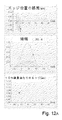
FIG. 15 shows the
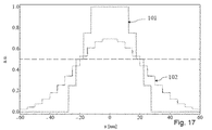
図17および図18は、図15および図16に類似した図に示される線量レベルの割り当て101によるCD=40nmの例を示す。同じカーネル91を使用して線量レベル畳み込み102を生成し、それによって、事実上、参照ツール(VSB)描画機の強度プロファイル104と一致する強度プロファイル103がもたらされた。線105は40nmのターゲット線を示す。
17 and 18 show an example of CD = 40 nm according to the
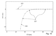
図19は、2つの描画機のタイプのΔCD=(CD*−CD)対CDの関係を示す。湾曲105は、MBW、この場合、5nmの1シグマぼけによる20nmのビームスポットでの四重グリッド露光の関係を示し、実際には偏向はなく、すなわち、平坦な関係105を有する。実際、理想の水平線からの湾曲105の偏向は、図12bの上部分にしめされるように、0.05nmの最大エッジ位置誤差の2倍に相当する<0.1nmである。対照的に、参照ツール、例えば、20nmの1シグマぼけによるVSB描画機では、100nmを下回るCD値のより大きい偏向があり、これは、ΔCD(CD)の値106がCDを減少させる負の値まで低下するからである。例えば、CD=30nmでは、CD*は、およそ−11nmのΔCDに相当するおよそ19nm(図16を参照)である。
FIG. 19 shows the relationship between ΔCD = (CD * -CD) vs. CD for two drawing machine types. The curvature 105 shows the relationship of quadruple grid exposure at a 20 nm beam spot with MBW, in this
図19を参照すると、カーネル91によって畳み込まれたMBWには、事実上、参照ツール(VSB)106と同じ性能107がもたらされる。図19aは、CDの関数として、ΔCDの湾曲107および106の値の間の差異を詳細に示す。30nm以上のCD値にとっての偏向は、0.25nmより小さい。これは、本発明による方法がCDといった重大なパラメータからのほんのわずかの小さな偏向によって非常に良好な程度まで参照ツールを模倣できることを示す。実際、(ii)MBWによるより小さなビームサイズを使用して、または、(iii)MBWにおけるターゲット上のより小さい物理的なグリッドを使用して、(i)カーネルをさらに適切に最適化することによって、偏向をさらに低減することができるはずである。
Referring to FIG. 19, the MBW convoluted by the kernel 91 provides virtually the
上記の1次元の例に加えて、二次元のシミュレーションが行われた。これについて、図20に示される等方性カーネル111を使用することができる。カーネル111はカーネル91(図14)を回転させることによって生成された。カーネル111を、(例えば、整数または実数)値のマトリックスの形でも表すことができる。例えば、例えば、図21は、整数マトリックス112としてのカーネル111の表示を示す。ここで、個々の値は、次の整数値に四捨五入され(例えば、212は211.765から四捨五入され)、値は、ΣKk、l=1に正規化する必要はない。カーネル111は22×22のサイズを有するが、最も多い実装形態では、5×5、7×7または11×11のサイズなどのより小さいカーネルは、処理要件を満たすのに十分であるが、当然ながら、より大きいカーネルも適切である場合がある。 In addition to the one-dimensional example above, a two-dimensional simulation was performed. For this, the isotropic kernel 111 shown in FIG. 20 can be used. Kernel 111 was generated by rotating kernel 91 (FIG. 14). Kernel 111 can also be represented in the form of a matrix of values (eg, integer or real). For example, FIG. 21 shows the display of kernel 111 as an integer matrix 112. Here, the individual values are rounded to the next integer value (eg, 212 is rounded from 211.765), and the values need not be normalized to ΣK k, l = 1. Kernel 111 has a size of 22x22, but in the most implementations, smaller kernels such as 5x5, 7x7 or 11x11 sizes are sufficient to meet the processing requirements, but of course However, larger kernels may also be appropriate.
カーネルは、任意のパターン算出の前に確定され、次いで、画素データに応用される。参照ツールに適合するMBWの画素データを得るように畳み込みによって算出が行われる。項目Kk、lを有するマトリックスカーネル112の例において、MBWの位置(i、j)(i−th列におけるj−th画素)で使用される各値Po i、jの値の算出は次のようになる。
Po i、j=Σk、l(Pi+k、j+l・Kk、l)/Ko (1)
式中、Pi、jは、元のパターンの位置(i、j)における画素値を示し、その合計は、カーネルマトリックスにおける指数一式に及び、定数Koはカーネルの正規化である。
Ko=Σk、lKk、l (2)
The kernel is fixed before any pattern calculation and then applied to the pixel data. The calculation is performed by convolution so as to obtain the pixel data of MBW that matches the reference tool. In the example of the matrix kernel 112 having the items K k, l , the calculation of the values of the respective values Po i, j used at the position (i, j) of MBW (jth pixel in the th column) is as follows. become that way.
P o i, j = Σ k, l (P i + k, j + l · K k, l ) / Ko (1)
In the equation, Pi and j indicate the pixel values at the positions (i, j) of the original pattern, the sum of which represents a set of exponents in the kernel matrix, and the constant Ko is the kernel normalization.
Ko = Σ k, l K k, l (2)
図22a〜cは、5×5のサイズのカーネル(図22b)の簡略化した例を示す。図22cにおける畳み込まれたパターンPo i、jにおける画素のうちの1つの値を得るために、カーネルは画素データに応用され、図22aにおけるそれらの画素のみが、上記の式(1)に従って畳み込み算出において使用される符号Pi+k、j+lによって指定される(この場合、独立した合計におけるオフセット指数kおよびjは値−2および+2に及ぶ)。 22a-c show a simplified example of a 5x5 size kernel (FIG. 22b). Convolved pattern P o i in Fig. 22c, in order to obtain the value of one of pixels in the j, the kernel is applied to pixel data, only those pixels in FIG. 22a is, according to the above formula (1) Specified by the codes Pi + k, j + l used in the convolution calculation (in this case, the offset indices k and j in the independent sum span the values -2 and +2).
図23a〜cは、30nm幅を有する線の3つの2Dシミュレーションを示す。当該線の半分のみが示されているが、これは、残りの半分が対称的な画像であるためである。最大線量に対する45%、50%および55%の線量レベルの等高線図が示されており、点線の矩形は30nmの線のターゲット形状を示す。図23aは、5nmの1シグマぼけによる20nmのビームサイズおよび四重グリッド露光(すなわち、5nmの物理的グリッドサイズ)を有するMBWを使用する時、長さが300nmの線のシミュレーションの結果を示す。50%の線量レベルは、(高いレジストのコントラスを前提とした)展開によって得られたレジストの外郭である。図23bは、参照ツール、例えば、20nmの1シグマぼけによるVSB描画機の相当するシミュレーションの結果を示し、30nmの線幅を有する線では、図23aに示されるMBWと比較して、線エッジが明確に短くなり、かつ、線量寛容度が低下することが結果として示されている。図23cは、露光される30nmの線を参照ツールの線と適合させるために、ターゲットと共に、図20のカーネル111によって畳み込まれたMBWによる(シミュレートされた)露光の結果を示す。図23bのプロファイルとの適合が優良であることは明らかである。 Figures 23a-c show three 2D simulations of lines with a width of 30 nm. Only half of the line is shown because the other half is a symmetrical image. Contours of dose levels of 45%, 50% and 55% relative to maximum dose are shown, with dotted rectangles indicating the target shape of the 30 nm line. FIG. 23a shows the results of a simulation of a line with a length of 300 nm when using an MBW with a beam size of 20 nm with a 1 sigma blur of 5 nm and a quadruple grid exposure (ie, a physical grid size of 5 nm). The 50% dose level is the resist outline obtained by deployment (assuming a high resist contrast). FIG. 23b shows the results of a corresponding simulation of a reference tool, eg, a VSB writer with 1 sigma blur at 20 nm, where a line with a line width of 30 nm has a line edge compared to the MBW shown in FIG. 23a. The results have been shown to be clearly shorter and less dose tolerant. FIG. 23c shows the result of (simulated) exposure by MBW convoluted by kernel 111 of FIG. 20 with the target to match the exposed 30 nm line with the line of the reference tool. It is clear that the fit with the profile of FIG. 23b is excellent.
マルチビーム描画機のMRMCカーネル
本発明のさらなる態様は、参照ツールがMBWタイプ自体のものである場合である。例えば、いくつかのMBW機が設置されるマスクショップの場合、本発明は、場合により様々な結像パラメータを有する種々のMBWの性能を適合させるように適切に使用可能である。さらなる有用なタスクは、MBWを参照ツールのより古いバージョンに適合させることである。
MRMC Kernel for Multi-Beam Drawer A further aspect of the invention is when the reference tool is of the MBW type itself. For example, in the case of a mask shop where several MBW machines are installed, the present invention can be appropriately used to adapt the performance of different MBWs, optionally with different imaging parameters. A further useful task is to adapt the MBW to older versions of the reference tool.
異方性カーネル、複数のカーネル、および、時間依存性
本発明によるカーネルは、XY平面内で等方性を有する必要はない。例えば、MBW機がマスクを描画し、計量による綿密な分析によって、マスク上で、X方向の線幅が匹敵するY方向の線幅とある程度まで異なっているという状況がある場合があり、別のMBWデバイスにおいてかかる状況を模倣するために、本発明の別の態様による1つの適切なアプローチは異方性カーネルを用いることである。異方性カーネルの例が図24Aおよび図24Bに示されている。特に、図24Aは、Y方向に沿った線幅の約2倍である、X方向に沿った広い線幅を有する異方性カーネル151を示す。対照的に、図24Bに描写されたカーネル153は、Y方向に沿ってより広い線幅による異方性を有する。図24Cは、図24aのカーネル151のマトリックス表示152を示す。ここでは、例えば、小数第2位で四捨五入した実数値として、(正規化されない)個々の値が示される。カーネルはX方向またはY方向の線に制限されないが、X/Y方向に対して随意の角度で指向された異方性にも応用可能であることに留意することは意味のあることである。
Anisotropic kernels, multiple kernels, and time-dependent kernels according to the invention need not be isotropic in the XY plane. For example, there may be a situation where the MBW machine draws a mask and, by meticulous analysis by weighing, the line width in the X direction differs to some extent from the comparable line width in the Y direction on the mask. To mimic this situation in MBW devices, one suitable approach according to another aspect of the invention is to use an anisotropic kernel. Examples of anisotropic kernels are shown in FIGS. 24A and 24B. In particular, FIG. 24A shows an
一方では、異方性カーネルは、MBWデバイスまたは他のタイプの参照ツールにおける既知の異方性を補償する方法も提供し、例えば、X方向の方への異方性を、Y方向の方への異方性を有するカーネルを使用して補償することができ、その逆も同様に(または随意の鉛直方向の軸に対して)可能である。 On the one hand, the anisotropic kernel also provides a method of compensating for known anisotropy in MBW devices or other types of reference tools, eg, anisotropy towards the X direction, towards the Y direction. It can be compensated using a kernel with anisotropy of, and vice versa (or with respect to any vertical axis).
カーネルの上記例は、例示の目的のみのものであり、カーネルのさらなる実装形態およびかなりの重要性を有する他のタスクへの応用は当業者には自明であることに留意することも重要である。 It is also important to note that the above examples of kernels are for illustration purposes only and that further implementations of the kernel and its application to other tasks of considerable importance will be obvious to those skilled in the art. ..
カーネルの多くの可能な変形のうちの1つは、時間依存値を含む。例えば、描画プロセス中の時間変動f(t)が理論的考察および/または実験データから既知であるとする場合、かかる時間変動を実装することができる。これによって、レジストのエージングといった時間依存プロセスを考慮することができる。レジスト感度の変形が時間関数f(t)として既知である場合、カーネルにおける関連項目を入力する追加因数として、この関数を使用することができる。すなわち、Kk、l=K’k、l・f(t)であり、式中、(K’k、l)は、最初の時間依存カーネル、例えば、露光プロセス開始に有効なカーネルである。代替的にはまたは組み合わせて、粒子ビームが時間によって変動する場合がある全電流を有する光源から生成される場合、時間依存性は、光源から放出された全電流のゆらぎ関数に相当する関数を含むことができ、このことは、算出プロセスの前に実験的に確定されている。 One of the many possible variants of the kernel contains time-dependent values. For example, if the time variation f (t) during the drawing process is known from theoretical considerations and / or experimental data, such time variation can be implemented. This allows time-dependent processes such as resist aging to be considered. If the variant of resist sensitivity is known as the time function f (t), this function can be used as an additional factor to enter the relevant items in the kernel. That is, K k, l = K'k, l · f (t), and in the equation, ( K'k, l ) is the first time-dependent kernel, for example, a kernel effective for starting the exposure process. Alternatively or in combination, if the particle beam is generated from a light source with a total current that may fluctuate over time, the time dependence includes a function that corresponds to the fluctuation function of the total current emitted from the light source. This can be done experimentally before the calculation process.
本発明の別の態様は、1つの描画プロセス内で複数のカーネルを使用可能であることである。例えば、ターゲットの様々な領域に対して様々なカーネルを使用することができる。これは、参照ツールが、例えば、不均一な異方性といった、露光されるターゲット上の領域にわたる可変の結像性質を示す場合に有利である。また、既に述べたように、例えば、PDデバイス内の様々なアパーチャアレイ間を切り換えることによって、ビームサイズを、例えば、20nm〜10nmで、描画プロセス中に変更することができる(特許文献6を参照)。この場合、第1のカーネルは20nmのビームサイズによる露光に使用され、第2のカーネルは10nmのビームサイズによる露光に使用される。 Another aspect of the invention is the ability to use multiple kernels within a single drawing process. For example, different kernels can be used for different areas of the target. This is advantageous if the reference tool exhibits variable imaging properties over the area on the exposed target, for example non-uniform anisotropy. Also, as already mentioned, the beam size can be changed during the drawing process, for example, at 20 nm to 10 nm, by switching between various aperture arrays in the PD device (see Patent Document 6). ). In this case, the first kernel is used for exposure with a beam size of 20 nm and the second kernel is used for exposure with a beam size of 10 nm.
データ経路
図25は、本発明に照らして、データ経路170のフローチャートを示す。データ経路は、リアルタイムで描画ツールの処理システム18(図1)において行われるのが好ましく、変形では、データ経路の算出の一部または全てを、例えば、適切なコンピュータにおいて、前もって行うことができる。
Data Path FIG. 25 shows a flow chart of the
完全なパターン画像は膨大な量の画像データを含むが、これは、そのデータの効率的な計算のために、好ましくはリアルタイムで、露光される画素データを生成する高速データ経路が適切であるからである。露光されるパターンは、典型的には、例えば、矩形、台形、または、大まかな多角形のような幾何学的形状を収集したものとして、ベクトルフォーマットで記載され、これによって、典型的には、より良いデータ圧縮が与えられ、従って、データ記憶に対する要件が低減する。従って、データ経路は3つの主要な部分から成る。
−ベクトルベースの物理的補正プロセス(ステップ160)
−ベクトルを画素データに翻訳するためのラスター化プロセス(ステップ161〜164)、および、
−描画プロセスでの一時的な記憶のために画素データをバッファに保留すること(ステップ165)。
A complete pattern image contains a huge amount of image data, because a fast data path that produces the pixel data to be exposed is suitable, preferably in real time, for efficient computation of that data. Is. The pattern to be exposed is typically described in vector format as a collection of geometric shapes, such as rectangles, trapeziums, or rough polygons, thereby typically. Better data compression is given, thus reducing the requirement for data storage. Therefore, the data path consists of three main parts.
-Vector-based physical correction process (step 160)
-Rasterization process for translating vectors into pixel data (steps 161-164), and
-Holding pixel data in a buffer for temporary storage in the drawing process (step 165).
データ経路は、ステップ160で露光されるパターンPDATAが供給されると開始する。参照ツールが、例えば、VSB描画ツールと適合するものとする場合、例えば、図23bに示されるように、線エッジが短くなると、特定の描画性質について補正するために、前回のステップ(図示せず)で既に修正されていてもよい。ステップ160において、一般的に、露光されるパターンPDATAは、場合によって幾何学形状の重複部分と共に、多数の小さなデータの塊に分裂する。ベクトルドメインにおいて応用することができる補正(例えば、近接効果の補正)を、場合によって並行に、全ての塊に対して独立して行うことができ、結果として得られるデータを、続くステップの計算速度を改善するようにソートしかつコーディングする。出力は、全ての塊が幾何学的形状の収集を含有する場合の、塊の収集である。
The data path begins when the pattern PDATA exposed in
段階161:ラスター化RAST。あらゆる塊の幾何学的形状をラスターグラフィックスアレイに変換する。この場合、画素グレーレベルは、相当するアパーチャ画像の物理的な線量を表す。完全に幾何学形状内にあるあらゆる画素に多角形の色が割り当てられ、それに対し、幾何学形状のエッジを交差する画素の色を、幾何学形状によって覆われた画素のわずかな領域ごとに重み付けする。この方法は、幾何学形状の領域とラスター化後の総線量との間の線的関係を暗示している。最初に、線量を浮動総数点数として算出し、その後にようやく、PDデバイスによってサポートされる線量値の離散集合に変換する。ラスター化の結果、画素データは、対応する画素の公称線量値Pを表す浮動小数点数のフォーマットのものになる。 Stage 161: Rasterized LAST. Converts the geometry of any chunk into a raster graphics array. In this case, the pixel gray level represents the physical dose of the corresponding aperture image. Polygonal colors are assigned to every pixel that is completely within the geometry, whereas the color of the pixels that intersect the edges of the geometry is weighted by a small area of pixels covered by the geometry. To do. This method implies a linear relationship between the area of geometry and the total dose after rasterization. First, the dose is calculated as a floating total point, and then finally converted into a discrete set of dose values supported by the PD device. As a result of the rasterization, the pixel data is in the form of a floating point number representing the nominal dose value P of the corresponding pixel.
段階162:カーネル適合KERM。既定のMRMCカーネルを画素データに応用する。これは、上述のカーネルによる畳み込む画素データによって行われる。好ましくは、リアルタイムの処理速度を達成するために、十分な数の並列CPUおよびGPUが使用される。畳み込みカーネルは典型的には、数十ナノメートルのぼけの範囲に対して作用するため、効果的な方法で算出プロセスを並列化することができる。この場合、ビームアレイの画素データを様々なCPUおよび/またはGPU上で分散させる。 Stage 162: Kernel-compliant KERM. Apply the default MRMC kernel to pixel data. This is done by the pixel data convolved by the kernel described above. Preferably, a sufficient number of parallel CPUs and GPUs are used to achieve real-time processing speeds. Convolution kernels typically work over a range of tens of nanometers of blur, allowing the calculation process to be parallelized in an effective way. In this case, the pixel data of the beam array is distributed on various CPUs and / or GPUs.
段階163:アパーチャフィールド上でビーム50の均一な電流密度からの偏向の補償といった、他の画素ベースの補正CORR、および/または、DAP30における個々の欠陥のあるビーム偏向装置の補正。この種類の補正方法は、本発明の一部を形成せず、ここでは論じない。
Step 163: Other pixel-based correction CORRs, such as compensation for deflection from the uniform current density of the
段階164:ディザリングDITH。ディザリングプロセスは、既定のグレー値スケールに基づいて、畳み込まれた、場合によって補正される線量値データPoをグレー値データに変換する。これは、オーバーサンプリングと組み合わせて、単一のアパーチャに対して利用可能な線量値の離散集合よりもさらに精細な線量変動を可能にする近傍画素に対して丸め誤差が平均になることを徹底する、位置依存丸めプロセスであり、視像データを画素グラフィックスに変換するために既知のアルゴリズムによって実現可能である。実際の補正(例えば、欠陥のあるアパーチャの補正)に応じたディザリング直前または直後に、さらなる補正が画素ドメインにおいて応用可能であるとした場合、この段階で(本発明の一部ではない)このようなさらなる補正を応用することができる。 Stage 164: Dithering DITH. The dithering process converts the convoluted, optionally corrected dose value data Po into gray value data based on a default gray value scale. This, in combination with oversampling, ensures that rounding errors are averaged for nearby pixels, which allows finer dose variation than the discrete set of dose values available for a single aperture. It is a position-dependent rounding process, which can be realized by known algorithms for converting visual data into pixel graphics. At this stage (not part of the present invention), if further corrections are applicable in the pixel domain immediately before or after dithering according to the actual corrections (eg, corrections for defective apertures). Further corrections such as these can be applied.
段階165:画素パッケージング、PPACK。段階164から得られる画素画像は、配置グリッドシーケンスに従ってソートされ、描画ツールの処理システム18(図1)において設けられた画素バッファPBUFに送信される。画素データは、十分なデータ量、典型的には、少なくとも、ストライプの露光を引き起こすストライプの長さが存在するまで、バッファに保留される(図7を参照)。描画プロセス中にバッファからデータを取り出す。ストライプが描画された後に、上述したプロセスは、次のストライプなど、次の範囲のパターンデータを新たに開始する。
Stage 165: Pixel packaging, PPACK. The pixel images obtained from
適合する性能を満たすためのMRMCカーネルの較正
VSBツール、または、(一般に)参照ツールのデータ準備には通常、図19と共に上述されるように、CD変化を線幅の関数として考慮するために補正関数を使用する。さらに、進歩的な半導体ユーザは、洗練された型を応用して、CD値、線端短縮およびコーナープルバック半径、ならびに、関連のパターン特性を測定するのに対し、ベクトル入力データ、基本的に、線量割り当ておよびオプションとして形状も修正することによって、意図した形状からの偏向を補償する。この最適化は、どれくらいの並列コンピュータを使用するかに応じて計算時間の多くの時間または日にちを要する場合が多い計算集中シミュレーションに基づいており、その算出は、特定のビーム、ならびに、線量分布(点広がり関数)、レジストぼけ(例えば、CAR、すなわち、化学増幅型レジストにおける酸拡散効果)、および、入力数としてのレジストコントラストといったプロセス特性に基づいている。最終的に、あるVSB描画パラメータ(またはより一般的には、該当の参照ツールの描画パラメータ)を前提とすると、ぼけ関連のCD誤差またはコーナー丸めといった非常に重要な補正は、データ修正によって行われる。最も単純な場合、ほんのより小さいぼけである可能性がある、異なる描画性質をMBWが有する場合、意図されたパターンは、VSBツール(参照ツール)のために準備されたデータによって直接的に得られることはない。一般的な場合、ぼけだけでなく、点広がり関数(線量分布関数の2Dプロファイル)は、荷電粒子光学システムにおける差異によって、著しく偏向する。
Calibration of the MRMC Kernel to Meet Compliant Performance The data preparation of the VSB tool, or (generally) the reference tool, is usually corrected to consider the CD change as a function of line width, as described above with FIG. Use a function. In addition, progressive semiconductor users apply sophisticated molds to measure CD values, line end shortening and corner pullback radii, as well as related pattern characteristics, whereas vector input data, basically, Compensate for deviations from the intended shape by dose allocation and optionally shape modification. This optimization is based on a computational intensive simulation, which often takes many hours or days of computational time, depending on how many parallel computers are used, and the computation is based on a specific beam, as well as the dose distribution ( It is based on process characteristics such as point spread function), resist blur (eg, CAR, the acid diffusion effect in chemically amplified resists), and resist contrast as the number of inputs. Ultimately, given some VSB drawing parameters (or more generally, the drawing parameters of the reference tool in question), very important corrections such as blur-related CD errors or corner rounding are made by data correction. .. In the simplest case, if the MBW has different drawing properties, which can be just a smaller blur, the intended pattern is obtained directly by the data prepared for the VSB tool (reference tool). There is no such thing. In the general case, the point spread function (2D profile of the dose distribution function), as well as the blur, is significantly deflected by the differences in the charged particle optical system.
実際の応用では、これは、VSBツールまたは他の参照ツールを使用して、同じ製品のマスクを作ることも望むツールユーザは、他の参照ツールがVSBの特定の誤差に適合しない限り、または、換言すると、リソグラフィ結果における差異を最小限に抑えることでVSM描画性質を模倣するようにするオン線補正が設けられていない限り、MBW機の生産性を高めることから利益を得ることはできない。このさらなる特徴によって、MBWは、VSB描画にも使用される同じデータに対して使用可能であり、これによって、VSBツールが依然使用される限り、MBWの有用性が非常に高まる。 In practical application, this is also a tool user who wants to make a mask of the same product using VSB tool or other reference tool, unless the other reference tool fits the specific error of VSB, or In other words, one cannot benefit from increasing the productivity of MBW machines unless on-line correction is provided to mimic VSM drawing properties by minimizing differences in lithography results. This additional feature allows the MBW to be used for the same data that is also used for VSB drawing, which greatly enhances the usefulness of the MBW as long as the VSB tool is still used.
MRMCカーネルの確定
参照ツールの強度プロファイル、例えば、VSB描画機の強度プロファイル61、62は既知であり、例えば、実験的に確定されていることは、かなりありふれたことである。代替的には、参照ツールにとって線形グラフ(図19)が既知である場合があり、当該線形グラフにより、強度プロファイルを算出することができ、または、データの実験セット、例えば、参照ツールによって印刷される、可変の線量または可変の設計幅の関数としての線幅のセットを初期データとして利用して、強度プロファイルを確定することができる。MRMCカーネルの確定/最適化のために、ここでは、強度プロファイルが既知であることを前提とする(数学的に、例えば、ぼけおよび他の結像アーチファクトを含む、デルタ関数のような無限に小さいパターン要素が、露光中基板上で生成する線量分布である点広がり関数)。
MRMC Kernel Confirmation Reference tool intensity profiles, such as VSB writer intensity profiles 61, 62, are known, and experimentally determined, for example, are fairly commonplace. Alternatively, a linear graph (FIG. 19) may be known to the reference tool, from which the intensity profile can be calculated, or printed by an experimental set of data, such as the reference tool. A set of line widths as a function of variable dose or variable design width can be used as initial data to determine the intensity profile. For the determination / optimization of the MRMC kernel, it is assumed here that the intensity profile is known (mathematical, eg, infinitely small, such as a delta function, including blur and other imaging artifacts. The point spread function, where the pattern element is the dose distribution generated on the substrate during exposure).
MRMCの確定および最適化は典型的には反復プロセスであり、この場合、MRMCカーネルを表すある点の数が体系的におよび/または確率的に可変であることで、目的関数(性能指数)に関して最適化されるようにする。目的関数は、例えば、線形関数における差異の積分である可能性があり(図19Aを参照)、または、図24aおよび図24bを参照して論じたように、指向性の線幅変動を最適化する場合、対象の線方向についての線幅間の差異である可能性がある。 MRMC determination and optimization is typically an iterative process, where the number of points representing the MRMC kernel is systematically and / or stochastically variable, with respect to the objective function (figure of merit). To be optimized. The objective function can be, for example, an integral of the differences in a linear function (see FIG. 19A) or, as discussed with reference to FIGS. 24a and 24b, optimizing directional line width variation. If so, it may be a difference between the line widths with respect to the target line direction.
一般的に、このような最適化を、現状技術において周知の数学的原理を使用した従来のアルゴリズムで行うことができる。使用可能な1つの標準的な方法論は、傾斜法、または、線形回帰法である。開始関数として、例えば、単一のガウス関数の形で図26dにおいて例として示される参照ツールの強度プロファイルが使用される。実際、多くの場合、強度プロファイルは既に、最終カーネルに対して適切に良好な近似を提示しており、さらなる最適化は、適合の精密度においてより高い要求に従うためだけに必要とされる。ぼけの差異が大きいほど、より良好に適合作業が行われ、より大きなぼけによって与えられる強度分布によってさらなるカーネル関数が支配されることになる。 In general, such optimization can be performed by conventional algorithms using mathematical principles well known in the current technology. One standard methodology that can be used is the gradient method, or the linear regression method. As the starting function, for example, the intensity profile of the reference tool shown as an example in FIG. 26d in the form of a single Gaussian function is used. In fact, in many cases, the strength profile already presents a reasonably good approximation to the final kernel, and further optimization is needed only to meet the higher requirements in the precision of the fit. The greater the blur difference, the better the fitting work will be, and the intensity distribution given by the larger blur will dominate further kernel functions.
図26a〜dは、最適なカーネルを見つけるために、線形回帰算出に対して、開始関数として適切なカーネル関数の例を示す。あるいは、それらカーネル関数の例は、(後続の最適化を行わずに)直接的に行う複数のタスクには十分である場合がある。特に、図26aに描写される矩形関数を使用して、例えば、「移動平均化」といったある目的を達成することもでき、図26bの三角関数は、加重平均化を行うのに適切であり、または、図26cにおいて描写されるsinc関数を使用して、「エッジ強調」または「パターン選択」フィルタリングを行うことができ、この場合、カーネルは差別化の効果を有し、最終的に、図26dはガウス形状を示す。sinc形状のカーネルの負の値は、基板上の負の線量値を回避するために、ゼロといった非負のカットオフ値によって置き換えられる公称の負の線量がもたらされる場合がある。 FIGS. 26a-d show an example of a kernel function suitable as a starting function for linear regression calculation in order to find the optimum kernel. Alternatively, these kernel function examples may be sufficient for multiple tasks performed directly (without subsequent optimization). In particular, the rectangular function depicted in FIG. 26a can also be used to achieve a certain purpose, for example, "moving averaging", and the trigonometric function of FIG. 26b is suitable for performing weighted averaging. Alternatively, the sinc function depicted in FIG. 26c can be used for "edge enhancement" or "pattern selection" filtering, in which case the kernel has a differentiating effect and finally in FIG. 26d. Indicates a Gaussian shape. Negative values in sinc-shaped kernels may result in a nominal negative dose that is replaced by a non-negative cutoff value such as zero to avoid negative dose values on the substrate.
当然ながら、MBW自体は、(スポットの幅および点広がり関数によって)ぼけを有することになる。MBWのぼけは、通常、(少なくとも1.5、典型的には3またはそれ以上の因数で)ターゲット上に描画される線幅と比較すると非常に小さく、参照ツールのぼけと比較するとさらに一層小さい。従って、MBWのぼけを無視して、少なくとも第1の段階でほとんど損傷ないカーネルを確定することができる。反復アプローチにおいて、これは、反復がMBWのぼけの効果を暗黙のうちに考慮することになるため、安全な手順である。実際、通常、カーネルにおけるMBWのぼけを無視することによって取り入れられた偏向は、既に第1の段階で端にあるのみであることが分かった。 Of course, the MBW itself will have blur (depending on the width of the spot and the point spread function). MBW blur is usually very small compared to the line width drawn on the target (at least 1.5, typically with a factor of 3 or more), and even smaller compared to the reference tool blur. .. Therefore, it is possible to ignore the blurring of MBW and determine a kernel that is hardly damaged at least in the first stage. In an iterative approach, this is a safe procedure as it will implicitly consider the effects of MBW blur. In fact, it turns out that the bias usually introduced by ignoring the MBW blur in the kernel is already only at the edge in the first stage.
Claims (13)
前記パターン画定デバイスにおいて、前記複数のブランキングアパーチャ(24、33、43)は、前記ブランキングアパーチャの相互の位置を画定する既定の配列で配置され、各ブランキングアパーチャは、各露光間隔中に前記ターゲット上に生成された相当するアパーチャ画像上に、各ブランキングアパーチャを通って露光する線量値に関して選択的に調節可能であり、前記線量値は離散グレースケールから選択された各値を有し、
前記所望のパターンの描画プロセス中に、一連の露光間隔(T1)が設けられ、各露光間隔で、前記ブランキングアパーチャが、前記ターゲット(16)上へ写像されるため、相当する複数のアパーチャ画像(b1、bi0、bi1)が生成され、
i)前記ターゲット上の画像領域上に、グラフィカル表示(72、101)として前記所望のパターンを与えることであって、前記グラフィカル表示(72、101)は既定の画素間隔の解像度を有し、前記画素間隔は前記画像領域内の前記画素の近接する位置間の公称距離より大きい、所望のパターンを与えることと、
ii)畳み込みカーネル(91、111)を与えることであって、前記カーネルは前記グラフィカル表示の要素から画素群へのマッピングを記述し、前記画素群は前記要素の公称位置を中心とする、畳み込みカーネル(91、111)を与えることと、
iii)前記畳み込みカーネル(91、111)による前記グラフィカル表示(72、101)の畳み込みによって、前記多数の画素上で画定された画素ラスターグラフィックス(ps)として公称露光パターンを算出することであって、前記公称露光パターンは前記ターゲット上に公称線量分布を作成するのに適切である、公称露光パターンを算出することと、を含み、
前記畳み込みカーネルは、前記荷電粒子マルチビーム処理装置によってエミュレートされた参照描画装置の点広がり関数を表す、方法。 In the charged particle multi-beam processing apparatus (1), a method of calculating an exposure pattern for exposing a desired pattern on a target (16), in which the particle beam (Ib, 50) is directed toward a pattern defining device (4). irradiation morphism, and the pattern definition device (4), in order to draw the desired pattern by exposing a plurality of pixels in the image area on the target (px), a plurality of said particle beam passes through It has an aperture array (26) composed of blanking apertures (24, 33, 43).
In the pattern definition device, said plurality of blanking apertures (24,33,43), said blanking mutual positional ranking aperture is placed in the default sequence defining a respective blanking aperture, during each exposure interval The dose value is selectively adjustable with respect to the dose value exposed through each blanking aperture on the corresponding aperture image generated on the target, and the dose value has each value selected from the discrete grayscale. And
During the drawing process of the desired pattern, a series of exposure intervals (T1) are provided, and at each exposure interval, the blanking aperture is mapped onto the target (16), so that a plurality of corresponding aperture images (B1, bi0, bi1) is generated and
i) To provide the desired pattern as a graphical display (72, 101) on an image area on the target, the graphical display (72, 101) has a resolution of a predetermined pixel spacing and said. pixel spacing is greater than the nominal distance between a position adjacent the pixel of the image area, and to provide a desired pattern,
ii) Given a convolution kernel (91, 111), the kernel describes a mapping from the elements of the graphical display to a pixel group, which is a convolution kernel centered on the nominal position of the element. Giving (91, 111) and
iii) By convolving the graphical display (72, 101) by the convolution kernel (91, 111), the nominal exposure pattern is calculated as pixel raster graphics (ps) defined on the large number of pixels. The nominal exposure pattern comprises calculating the nominal exposure pattern, which is suitable for creating a nominal dose distribution on the target.
A method in which the convolution kernel represents a point spread function of a reference drawing device emulated by the charged particle multi-beam processor.
iv)前記公称露光パターンから、アパーチャ画像の露光による前記描画プロセスによって前記所望のパターンを露光するのに適切な露光パターンを生成する、
さらなるステップを有する、請求項1に記載の方法。 The drawing process produces overlapping aperture images, which have a nominal width (b) that is a multiple of the distance (e) between pixel positions of adjacent aperture images generated on the target. Have and
iv) From the nominal exposure pattern, an exposure pattern suitable for exposing the desired pattern is generated by the drawing process by exposing the aperture image.
The method of claim 1, further comprising a step.
照明システム(3)と、
パターン画定デバイス(4)と、
投影光学システム(5)と、を備え、
前記照明システム(3)は、前記荷電粒子のビームを作り、当該ビームを広範なビーム(Ib)にして前記パターン画定デバイス(4)を照射するように構成され、前記パターン画定デバイス(4)は、照射している前記ビームの形状を複数のサブビームで構成される構造化ビームにするように構成され、前記投影光学システム(5)は、前記パターン画定デバイスにおいて画定された前記ビーム形状の画像を前記ターゲット(16)上に投影することで、前記ターゲット上の画像領域内に複数の画素(px)を露光するように構成され、
前記パターン画定デバイス(4)は、サブビーム(51、52)を形成する複数のブランキングアパーチャ(24、33、43)で構成されたアパーチャアレイ(26)を備え、前記複数のブランキングアパーチャ(24、33、43)は、前記複数のブランキングアパーチャの相互の位置を画定する既定の配列で配置され、各ブランキングアパーチャは、各露光間隔の間に前記ターゲット上に生成された相当するアパーチャ画像上に、各ブランキングアパーチャを通って露光する線量値に関して選択的に調節可能であり、前記線量値は離散グレースケールから選択された各値を有し、
前記所望のパターンの描画プロセス中に、一連の露光間隔(T1)が設けられ、各露光間隔で、前記ブランキングアパーチャが、前記ターゲット(16)上へ写像されるため、相当する複数のアパーチャ画像(b1、bi0、bi1)が生成され、
前記処理装置は、参照描画装置における所望のパターンの描画プロセスをエミュレートするように構成され、前記参照描画装置は、前記処理装置によって生成された前記アパーチャ画像の公称画素間隔より大きい画素間隔の解像度を有する点広がり関数を有し、前記所望のパターンを、前記処理装置によって描画可能な公称露光パターンに変換するために、請求項1〜12のうちいずれか一項に記載の方法が使用される、荷電粒子マルチビーム処理装置(1)。 A charged particle multi-beam processing device (1) for exposing a target (16) with a structured beam of charged particles.
Lighting system (3) and
Pattern demarcation device (4) and
Equipped with a projection optical system (5)
The illumination system (3) is configured to create a beam of the charged particles, turn the beam into a broad beam (Ib) and irradiate the pattern defining device (4), the pattern defining device (4). , consists of the shape of the beam that is irradiated to the structured beam composed of sub-beams of multiple, the projection optical system (5), the image of the beam shape defined in the pattern definition device Is configured to expose a plurality of pixels (px) in the image area on the target by projecting the image onto the target (16).
The pattern defining device (4) includes an aperture array (26) composed of a plurality of blanking apertures (24, 33, 43) forming subbeams (51, 52), and the plurality of blanking apertures (24). , 33, 43) is placed in the default sequence that defines the mutual position of said plurality of blanking apertures, each blanking aperture corresponds created on the target during each exposure interval aperture On the image, the dose values exposed through each blanking aperture can be selectively adjusted, said dose values having each value selected from discrete grayscale.
During the drawing process of the desired pattern, a series of exposure intervals (T1) are provided, and at each exposure interval, the blanking aperture is mapped onto the target (16), so that a plurality of corresponding aperture images (B1, bi0, bi1) is generated and
The processing device is configured to emulate a drawing process of a desired pattern in a reference drawing device, and the reference drawing device has a pixel spacing resolution greater than the nominal pixel spacing of the aperture image generated by the processing device. The method according to any one of claims 1 to 12 is used in order to convert the desired pattern into a nominal exposure pattern that can be drawn by the processing apparatus. , Charged particle multi-beam processing device (1).
Applications Claiming Priority (4)
| Application Number | Priority Date | Filing Date | Title |
|---|---|---|---|
| EP14176563 | 2014-07-10 | ||
| EP14176563.6 | 2014-07-10 | ||
| EP14199183 | 2014-12-19 | ||
| EP14199183.6 | 2014-12-19 |
Publications (3)
| Publication Number | Publication Date |
|---|---|
| JP2016018995A JP2016018995A (en) | 2016-02-01 |
| JP2016018995A5 JP2016018995A5 (en) | 2021-04-22 |
| JP6892214B2 true JP6892214B2 (en) | 2021-06-23 |
Family
ID=53491459
Family Applications (2)
| Application Number | Title | Priority Date | Filing Date |
|---|---|---|---|
| JP2015134558A Active JP6892214B2 (en) | 2014-07-10 | 2015-07-03 | Customization of particle beam lithography system using convolution kernel |
| JP2015134559A Active JP6890373B2 (en) | 2014-07-10 | 2015-07-03 | Compensation for imaging deflection in particle beam lithography machines using a convolution kernel |
Family Applications After (1)
| Application Number | Title | Priority Date | Filing Date |
|---|---|---|---|
| JP2015134559A Active JP6890373B2 (en) | 2014-07-10 | 2015-07-03 | Compensation for imaging deflection in particle beam lithography machines using a convolution kernel |
Country Status (4)
| Country | Link |
|---|---|
| US (2) | US9520268B2 (en) |
| EP (2) | EP2927748B1 (en) |
| JP (2) | JP6892214B2 (en) |
| KR (2) | KR102357185B1 (en) |
Families Citing this family (33)
| Publication number | Priority date | Publication date | Assignee | Title |
|---|---|---|---|---|
| EP2937889B1 (en) | 2014-04-25 | 2017-02-15 | IMS Nanofabrication AG | Multi-beam tool for cutting patterns |
| EP3358599B1 (en) | 2014-05-30 | 2021-01-27 | IMS Nanofabrication GmbH | Compensation of dose inhomogeneity using row calibration |
| JP6892214B2 (en) * | 2014-07-10 | 2021-06-23 | アイエムエス ナノファブリケーション ゲーエムベーハー | Customization of particle beam lithography system using convolution kernel |
| US9568907B2 (en) | 2014-09-05 | 2017-02-14 | Ims Nanofabrication Ag | Correction of short-range dislocations in a multi-beam writer |
| JP5816739B1 (en) * | 2014-12-02 | 2015-11-18 | 株式会社ニューフレアテクノロジー | Multi-beam blanking aperture array device and method for manufacturing multi-beam blanking aperture array device |
| US9658538B2 (en) * | 2014-12-19 | 2017-05-23 | Taiwan Semiconductor Manufacturing Company, Ltd. | System and technique for rasterizing circuit layout data |
| US9653263B2 (en) | 2015-03-17 | 2017-05-16 | Ims Nanofabrication Ag | Multi-beam writing of pattern areas of relaxed critical dimension |
| EP3096342B1 (en) | 2015-03-18 | 2017-09-20 | IMS Nanofabrication AG | Bi-directional double-pass multi-beam writing |
| US10410831B2 (en) | 2015-05-12 | 2019-09-10 | Ims Nanofabrication Gmbh | Multi-beam writing using inclined exposure stripes |
| JP6590542B2 (en) * | 2015-06-15 | 2019-10-16 | 株式会社ニューフレアテクノロジー | Charged particle beam drawing method and charged particle beam drawing apparatus |
| JP6727021B2 (en) * | 2016-04-26 | 2020-07-22 | 株式会社ニューフレアテクノロジー | Multi-charged particle beam irradiation device, multi-charged particle beam irradiation method, and multi-charged particle beam adjustment method |
| EP3258479B1 (en) * | 2016-06-13 | 2019-05-15 | IMS Nanofabrication GmbH | Method for compensating pattern placement errors caused by variation of pattern exposure density in a multi-beam writer |
| US10325756B2 (en) | 2016-06-13 | 2019-06-18 | Ims Nanofabrication Gmbh | Method for compensating pattern placement errors caused by variation of pattern exposure density in a multi-beam writer |
| CN109477848B (en) * | 2016-07-25 | 2023-07-18 | 西门子医疗保健诊断公司 | Systems, methods, and apparatus for identifying sample container lids |
| WO2018061960A1 (en) * | 2016-09-29 | 2018-04-05 | 大日本印刷株式会社 | Method and device for obtaining exposure intensity distribution in multibeam electron beam lithography device |
| JP6881168B2 (en) * | 2016-09-29 | 2021-06-02 | 大日本印刷株式会社 | Method and device for obtaining exposure intensity distribution in multi-beam electron beam lithography system |
| WO2018121967A1 (en) * | 2016-12-28 | 2018-07-05 | Asml Netherlands B.V. | Methods of determining scattering of radiation by structures of finite thicknesses on a patterning device |
| EP3355337B8 (en) * | 2017-01-27 | 2024-04-10 | IMS Nanofabrication GmbH | Advanced dose-level quantization for multibeam-writers |
| US10325757B2 (en) | 2017-01-27 | 2019-06-18 | Ims Nanofabrication Gmbh | Advanced dose-level quantization of multibeam-writers |
| US10613413B1 (en) | 2017-05-31 | 2020-04-07 | Facebook Technologies, Llc | Ultra-wide field-of-view scanning devices for depth sensing |
| US10181200B1 (en) | 2017-06-28 | 2019-01-15 | Facebook Technologies, Llc | Circularly polarized illumination and detection for depth sensing |
| US10522329B2 (en) | 2017-08-25 | 2019-12-31 | Ims Nanofabrication Gmbh | Dose-related feature reshaping in an exposure pattern to be exposed in a multi beam writing apparatus |
| US10574973B2 (en) | 2017-09-06 | 2020-02-25 | Facebook Technologies, Llc | Non-mechanical beam steering for depth sensing |
| US11569064B2 (en) | 2017-09-18 | 2023-01-31 | Ims Nanofabrication Gmbh | Method for irradiating a target using restricted placement grids |
| US10651010B2 (en) | 2018-01-09 | 2020-05-12 | Ims Nanofabrication Gmbh | Non-linear dose- and blur-dependent edge placement correction |
| US10840054B2 (en) | 2018-01-30 | 2020-11-17 | Ims Nanofabrication Gmbh | Charged-particle source and method for cleaning a charged-particle source using back-sputtering |
| KR20200030806A (en) | 2018-09-13 | 2020-03-23 | 삼성전자주식회사 | Non-transitory computer-readable medium comprising image conversion model based on artificial neural network and method of converting image of semiconductor wafer for monitoring semiconductor fabrication process |
| US11099482B2 (en) | 2019-05-03 | 2021-08-24 | Ims Nanofabrication Gmbh | Adapting the duration of exposure slots in multi-beam writers |
| KR20210099516A (en) * | 2020-02-03 | 2021-08-12 | 아이엠에스 나노패브릭케이션 게엠베하 | Correction of blur variation in a multi―beam writer |
| KR20210132599A (en) | 2020-04-24 | 2021-11-04 | 아이엠에스 나노패브릭케이션 게엠베하 | Chargedparticle source |
| US11657207B2 (en) * | 2020-07-28 | 2023-05-23 | Synopsys, Inc. | Wafer sensitivity determination and communication |
| EP4095882A1 (en) | 2021-05-25 | 2022-11-30 | IMS Nanofabrication GmbH | Pattern data processing for programmable direct-write apparatus |
| JP2023138912A (en) | 2022-03-21 | 2023-10-03 | アイエムエス ナノファブリケーション ゲーエムベーハー | Correction of heat expansion in lithography drawing method |
Family Cites Families (134)
| Publication number | Priority date | Publication date | Assignee | Title |
|---|---|---|---|---|
| US1033741A (en) | 1911-02-08 | 1912-07-23 | Bona Sims | Armored tread for pneumatic tires. |
| US1420104A (en) | 1921-05-10 | 1922-06-20 | Edward W Howe | Brush-block-boring machine |
| US1903005A (en) | 1930-11-20 | 1933-03-28 | Gen Motors Corp | Oil pump screen |
| US2187427A (en) | 1937-09-11 | 1940-01-16 | Leslie H Middleton | Dashboard fuse mounting |
| US2820109A (en) | 1952-03-22 | 1958-01-14 | Cgs Lab Inc | Magnetic amplifier |
| US2920104A (en) | 1958-07-01 | 1960-01-05 | Vanderbilt Co R T | Stabilized solutions of a dithiocarbamate |
| DE2302938C3 (en) | 1973-01-22 | 1979-07-12 | Polymer-Physik Gmbh & Co Kg, 2844 Lemfoerde | Multi-stage accelerator for charged particles with high vacuum insulation |
| US4467211A (en) | 1981-04-16 | 1984-08-21 | Control Data Corporation | Method and apparatus for exposing multi-level registered patterns interchangeably between stations of a multi-station electron-beam array lithography (EBAL) system |
| JPH0628231B2 (en) | 1985-07-09 | 1994-04-13 | 富士通株式会社 | Electronic beam exposure method |
| US5103101A (en) | 1991-03-04 | 1992-04-07 | Etec Systems, Inc. | Multiphase printing for E-beam lithography |
| US5260579A (en) | 1991-03-13 | 1993-11-09 | Fujitsu Limited | Charged particle beam exposure system and charged particle beam exposure method |
| GB9107207D0 (en) | 1991-04-05 | 1991-05-22 | Tycho Technology Ltd | Mechanical manipulator |
| US5369282A (en) | 1992-08-03 | 1994-11-29 | Fujitsu Limited | Electron beam exposure method and system for exposing a pattern on a substrate with an improved accuracy and throughput |
| JP3206143B2 (en) | 1992-10-20 | 2001-09-04 | 富士通株式会社 | Charged particle beam exposure method |
| JP3437306B2 (en) | 1995-02-01 | 2003-08-18 | 富士通株式会社 | Charged particle beam exposure method and apparatus |
| US5841145A (en) | 1995-03-03 | 1998-11-24 | Fujitsu Limited | Method of and system for exposing pattern on object by charged particle beam |
| US6229595B1 (en) | 1995-05-12 | 2001-05-08 | The B. F. Goodrich Company | Lithography system and method with mask image enlargement |
| JP3565652B2 (en) | 1996-04-25 | 2004-09-15 | 富士通株式会社 | Transmission mask for charged particle beam exposure apparatus and exposure apparatus using the same |
| JP3335845B2 (en) | 1996-08-26 | 2002-10-21 | 株式会社東芝 | Charged beam drawing apparatus and drawing method |
| US6225637B1 (en) | 1996-10-25 | 2001-05-01 | Canon Kabushiki Kaisha | Electron beam exposure apparatus |
| US5847959A (en) | 1997-01-28 | 1998-12-08 | Etec Systems, Inc. | Method and apparatus for run-time correction of proximity effects in pattern generation |
| US5876902A (en) | 1997-01-28 | 1999-03-02 | Etec Systems, Inc. | Raster shaped beam writing strategy system and method for pattern generation |
| JP3085454B2 (en) | 1997-03-13 | 2000-09-11 | 日本電気株式会社 | Charged particle beam exposure method |
| JP3787417B2 (en) | 1997-06-11 | 2006-06-21 | キヤノン株式会社 | Electron beam exposure method and electron beam exposure apparatus |
| TR200001744T2 (en) | 1997-12-17 | 2000-12-21 | International Coatings Limited | Powder coating process. |
| US6552353B1 (en) | 1998-01-05 | 2003-04-22 | Canon Kabushiki Kaisha | Multi-electron beam exposure method and apparatus and device manufacturing method |
| US6014200A (en) | 1998-02-24 | 2000-01-11 | Nikon Corporation | High throughput electron beam lithography system |
| SE9800665D0 (en) | 1998-03-02 | 1998-03-02 | Micronic Laser Systems Ab | Improved method for projection printing using a micromirror SLM |
| US6043496A (en) | 1998-03-14 | 2000-03-28 | Lucent Technologies Inc. | Method of linewidth monitoring for nanolithography |
| JP2000056960A (en) | 1998-08-13 | 2000-02-25 | Ricoh Co Ltd | User interface device |
| US6252339B1 (en) | 1998-09-17 | 2001-06-26 | Nikon Corporation | Removable bombardment filament-module for electron beam projection systems |
| US6111932A (en) | 1998-12-14 | 2000-08-29 | Photoelectron Corporation | Electron beam multistage accelerator |
| US9188874B1 (en) | 2011-05-09 | 2015-11-17 | Kenneth C. Johnson | Spot-array imaging system for maskless lithography and parallel confocal microscopy |
| JP2000252198A (en) | 1999-03-02 | 2000-09-14 | Advantest Corp | Charged particle beam exposure system |
| JP2000260686A (en) | 1999-03-08 | 2000-09-22 | Toshiba Corp | Exposure method and aligner |
| KR100339140B1 (en) | 1999-04-28 | 2002-05-31 | 히로시 오우라 | Electron beam exposure apparatus |
| US6720565B2 (en) | 1999-06-30 | 2004-04-13 | Applied Materials, Inc. | Real-time prediction of and correction of proximity resist heating in raster scan particle beam lithography |
| US6472673B1 (en) | 1999-07-29 | 2002-10-29 | Ims Ionen-Mikrofabrikations Systeme Gmbh | Lithographic method for producing an exposure pattern on a substrate |
| WO2001039243A1 (en) | 1999-11-23 | 2001-05-31 | Ion Diagnostics, Inc. | Electron optics for multi-beam electron beam lithography tool |
| JP2001168018A (en) | 1999-12-13 | 2001-06-22 | Canon Inc | Device and method for exposing charged corpuscular beam, determining method for exposure correction data and method for producing device by applying the same method |
| JP4585661B2 (en) | 2000-03-31 | 2010-11-24 | キヤノン株式会社 | Electro-optical array, charged particle beam exposure apparatus, and device manufacturing method |
| WO2001075949A1 (en) | 2000-04-04 | 2001-10-11 | Advantest Corporation | Multibeam exposure apparatus comprising multiaxis electron lens and method for manufacturing semiconductor device |
| US6509955B2 (en) | 2000-05-25 | 2003-01-21 | Ball Semiconductor, Inc. | Lens system for maskless photolithography |
| US6473237B2 (en) | 2000-11-14 | 2002-10-29 | Ball Semiconductor, Inc. | Point array maskless lithography |
| DE10127836A1 (en) | 2001-06-08 | 2003-01-30 | Giesecke & Devrient Gmbh | Device for examining documents |
| US7302111B2 (en) * | 2001-09-12 | 2007-11-27 | Micronic Laser Systems A.B. | Graphics engine for high precision lithography |
| JP3730153B2 (en) | 2001-10-18 | 2005-12-21 | セイコーインスツル株式会社 | Printer cutter device |
| US6671975B2 (en) | 2001-12-10 | 2004-01-06 | C. William Hennessey | Parallel kinematic micromanipulator |
| DE10161152B4 (en) | 2001-12-12 | 2014-02-13 | Medical Intelligence Medizintechnik Gmbh | Positioning the treatment beam of a radiation therapy system by means of a hexapod |
| US6768125B2 (en) | 2002-01-17 | 2004-07-27 | Ims Nanofabrication, Gmbh | Maskless particle-beam system for exposing a pattern on a substrate |
| TW546595B (en) | 2002-07-23 | 2003-08-11 | Internet Motion Navigator Corp | Six-axis translation-type dynamic simulation device |
| KR100480609B1 (en) | 2002-08-09 | 2005-04-06 | 삼성전자주식회사 | Method of electron beam lithography |
| US6896037B2 (en) | 2002-10-29 | 2005-05-24 | Duramax Marine, Llc | Keel cooler with fluid flow diverter |
| US6767125B2 (en) | 2003-01-21 | 2004-07-27 | Red Devil Equipment Company | Keyed paint container holder for a paint mixer |
| US6962835B2 (en) | 2003-02-07 | 2005-11-08 | Ziptronix, Inc. | Method for room temperature metal direct bonding |
| JP2004282038A (en) | 2003-02-28 | 2004-10-07 | Canon Inc | Deflector, method for producing deflector, and charged particle beam exposure device using deflector |
| GB2399676B (en) | 2003-03-21 | 2006-02-22 | Ims Ionen Mikrofab Syst | Apparatus for enhancing the lifetime of stencil masks |
| US7138629B2 (en) | 2003-04-22 | 2006-11-21 | Ebara Corporation | Testing apparatus using charged particles and device manufacturing method using the testing apparatus |
| ATE449978T1 (en) | 2003-06-06 | 2009-12-15 | Nikon Corp | HOLDING DEVICE FOR OPTICAL ELEMENTS, LENS TUBE, EXPOSURE DEVICE AND PRODUCTION METHOD FOR COMPONENTS |
| GB2406704B (en) | 2003-09-30 | 2007-02-07 | Ims Nanofabrication Gmbh | Particle-optic electrostatic lens |
| DE102004025832A1 (en) | 2004-05-24 | 2005-12-22 | Carl Zeiss Smt Ag | Optics module for a lens |
| JP4313145B2 (en) | 2003-10-07 | 2009-08-12 | 株式会社日立ハイテクノロジーズ | Charged particle beam drawing method and charged particle beam drawing apparatus |
| GB2408143B (en) | 2003-10-20 | 2006-11-15 | Ims Nanofabrication Gmbh | Charged-particle multi-beam exposure apparatus |
| GB2408383B (en) | 2003-10-28 | 2006-05-10 | Ims Nanofabrication Gmbh | Pattern-definition device for maskless particle-beam exposure apparatus |
| GB2414111B (en) | 2004-04-30 | 2010-01-27 | Ims Nanofabrication Gmbh | Advanced pattern definition for particle-beam processing |
| GB2413694A (en) | 2004-04-30 | 2005-11-02 | Ims Nanofabrication Gmbh | Particle-beam exposure apparatus |
| JP4634076B2 (en) | 2004-06-30 | 2011-02-16 | キヤノン株式会社 | Charged particle beam exposure apparatus and device manufacturing method |
| JP2006079911A (en) | 2004-09-09 | 2006-03-23 | Hitachi High-Technologies Corp | Electron beam current measuring method, electron beam drawing apparatus, and electron beam detector |
| JP2006126823A (en) | 2004-09-30 | 2006-05-18 | Fujitsu Ltd | Variable rectangular electron beam exposure apparatus and pattern exposure formation method |
| JP4460987B2 (en) | 2004-09-30 | 2010-05-12 | 株式会社東芝 | Electron beam drawing method and magnetic recording medium manufacturing method |
| DE102004052994C5 (en) | 2004-11-03 | 2010-08-26 | Vistec Electron Beam Gmbh | Multi-beam modulator for a particle beam and use of the multi-beam modulator for maskless substrate structuring |
| GB2435348B (en) | 2004-11-17 | 2009-06-24 | Ims Nanofabrication Ag | Pattern lock system for particle-beam exposure apparatus |
| US7459247B2 (en) | 2004-12-27 | 2008-12-02 | Asml Netherlands B.V. | Lithographic apparatus and device manufacturing method |
| WO2006084298A1 (en) | 2005-02-11 | 2006-08-17 | Ims Nanofabrication Ag | Charged-particle exposure apparatus with electrostatic zone plate |
| WO2006107664A2 (en) | 2005-04-01 | 2006-10-12 | Trustees Of Stevens Institute Of Technology | Flexible parallel manipulator for nano-, meso-or macro-positioning with multi-degrees of freedom |
| JP4648087B2 (en) | 2005-05-25 | 2011-03-09 | キヤノン株式会社 | Deflector fabrication method, charged particle beam exposure apparatus, and device manufacturing method |
| EP1941528B9 (en) | 2005-09-06 | 2011-09-28 | Carl Zeiss SMT GmbH | Particle-optical arrangement with particle-optical component |
| JP4638327B2 (en) | 2005-10-17 | 2011-02-23 | 新日本工機株式会社 | Parallel mechanism device, parallel mechanism device calibration method, calibration program, and recording medium |
| KR101096954B1 (en) | 2006-01-31 | 2011-12-20 | 신에쓰 가가꾸 고교 가부시끼가이샤 | Polymer, resist protective coating material, and patterning process |
| EP2002458B1 (en) | 2006-04-03 | 2009-11-04 | IMS Nanofabrication AG | Particle-beam exposure apparatus with overall-modulation of a patterned beam |
| JP4758829B2 (en) * | 2006-06-06 | 2011-08-31 | 株式会社ニューフレアテクノロジー | Charged beam drawing apparatus and drawing method |
| JP4857963B2 (en) * | 2006-07-05 | 2012-01-18 | ソニー株式会社 | PATTERN EXTRACTION METHOD, PATTERN EXTRACTION DEVICE, AND SEMICONDUCTOR DEVICE MANUFACTURING METHOD |
| US7738077B2 (en) * | 2006-07-31 | 2010-06-15 | Asml Netherlands B.V. | Patterning device utilizing sets of stepped mirrors and method of using same |
| US20080142728A1 (en) | 2006-10-30 | 2008-06-19 | Applied Materials, Inc. | Mechanical scanner |
| JP5241195B2 (en) | 2006-10-30 | 2013-07-17 | アイエムエス ナノファブリカツィオン アーゲー | Charged particle exposure system |
| JP4932433B2 (en) | 2006-11-02 | 2012-05-16 | 株式会社ニューフレアテクノロジー | Electron beam drawing apparatus and electron beam drawing method |
| DE102008010123A1 (en) | 2007-02-28 | 2008-09-04 | Ims Nanofabrication Ag | Multibeam deflecting array device for maskless particle beam machining |
| NL2001369C2 (en) | 2007-03-29 | 2010-06-14 | Ims Nanofabrication Ag | METHOD FOR MASKLESS PARTICLE BEAMLIGHTING |
| US7930653B2 (en) | 2007-04-17 | 2011-04-19 | Micronic Laser Systems Ab | Triangulating design data and encoding design intent for microlithographic printing |
| JP5491704B2 (en) | 2007-05-14 | 2014-05-14 | イーエムエス ナノファブリカツィオン アーゲー | Pattern definition device having counter electrode array plate |
| JP4996978B2 (en) | 2007-05-28 | 2012-08-08 | 株式会社ニューフレアテクノロジー | Drawing method |
| DE102007034232B4 (en) | 2007-07-23 | 2012-03-01 | Bruker Daltonik Gmbh | Three-dimensional high frequency ion traps high trapping efficiency |
| EP2019415B1 (en) | 2007-07-24 | 2016-05-11 | IMS Nanofabrication AG | Multi-beam source |
| KR20100138907A (en) | 2008-02-05 | 2010-12-31 | 닐 테크놀로지 에이피에스 | A method for performing electron beam lithography |
| WO2009147202A1 (en) | 2008-06-04 | 2009-12-10 | Mapper Lithography Ip B.V. | Writing strategy |
| US8227768B2 (en) | 2008-06-25 | 2012-07-24 | Axcelis Technologies, Inc. | Low-inertia multi-axis multi-directional mechanically scanned ion implantation system |
| NL2003304C2 (en) | 2008-08-07 | 2010-09-14 | Ims Nanofabrication Ag | Compensation of dose inhomogeneity and image distortion. |
| DE102008053180B4 (en) | 2008-10-24 | 2012-07-12 | Advanced Mask Technology Center Gmbh & Co. Kg | Particle beam writing method, particle beam writing apparatus and maintenance method for the same |
| ATE527678T1 (en) | 2008-11-17 | 2011-10-15 | Ims Nanofabrication Ag | METHOD FOR MASKLESS PARTICLE BEAM EXPOSURE |
| EP2190003B1 (en) * | 2008-11-20 | 2014-10-01 | IMS Nanofabrication AG | Constant current multi-beam patterning |
| NL2003716A (en) * | 2008-11-24 | 2010-05-26 | Brion Tech Inc | Harmonic resist model for use in a lithographic apparatus and a device manufacturing method. |
| JP5634052B2 (en) | 2009-01-09 | 2014-12-03 | キヤノン株式会社 | Charged particle beam drawing apparatus and device manufacturing method |
| US8198601B2 (en) | 2009-01-28 | 2012-06-12 | Ims Nanofabrication Ag | Method for producing a multi-beam deflector array device having electrodes |
| EP2228817B1 (en) * | 2009-03-09 | 2012-07-18 | IMS Nanofabrication AG | Global point spreading function in multi-beam patterning |
| EP2251893B1 (en) | 2009-05-14 | 2014-10-29 | IMS Nanofabrication AG | Multi-beam deflector array means with bonded electrodes |
| EP2433295A2 (en) | 2009-05-20 | 2012-03-28 | Mapper Lithography IP B.V. | Dual pass scanning |
| WO2010134017A1 (en) | 2009-05-20 | 2010-11-25 | Mapper Lithography Ip B.V. | Method of generating a two-level pattern for lithographic processing and pattern generator using the same |
| CN102598199A (en) | 2009-09-18 | 2012-07-18 | 迈普尔平版印刷Ip有限公司 | Charged particle optical system with multiple beams |
| US8546767B2 (en) | 2010-02-22 | 2013-10-01 | Ims Nanofabrication Ag | Pattern definition device with multiple multibeam array |
| JP2011199279A (en) | 2010-03-18 | 2011-10-06 | Ims Nanofabrication Ag | Method for multibeam exposure on target |
| US8542797B2 (en) | 2010-09-24 | 2013-09-24 | Elekta Ab (Publ) | Radiotherapy apparatus configured to track a motion of a target region using a combination of a multileaf collimator and a patient support |
| JP5662756B2 (en) | 2010-10-08 | 2015-02-04 | 株式会社ニューフレアテクノロジー | Charged particle beam drawing apparatus and charged particle beam drawing method |
| JP5809419B2 (en) | 2011-02-18 | 2015-11-10 | 株式会社ニューフレアテクノロジー | Charged particle beam drawing apparatus and charged particle beam drawing method |
| JP5758325B2 (en) * | 2011-03-01 | 2015-08-05 | 株式会社ニューフレアテクノロジー | Charged particle beam drawing apparatus and charged particle beam drawing method |
| KR101854148B1 (en) | 2011-05-09 | 2018-05-03 | 삼성전자주식회사 | Electron beam exposure system and method for manufacturing reticle using the same |
| JP2013004216A (en) | 2011-06-14 | 2013-01-07 | Canon Inc | Electric charge particle beam lens |
| CN202204836U (en) | 2011-07-28 | 2012-04-25 | 辽宁省电力有限公司 | Insulated support for high-voltage test device |
| JP5886979B2 (en) | 2011-11-29 | 2016-03-16 | エーエスエムエル ネザーランズ ビー.ブイ. | Apparatus and method for converting a vector format representation of a desired device pattern for a lithographic apparatus, apparatus and method for supplying data to a programmable patterning device, lithographic apparatus, and device manufacturing method |
| JP5977941B2 (en) | 2011-12-19 | 2016-08-24 | 株式会社ニューフレアテクノロジー | Multi-charged particle beam writing apparatus and multi-charged particle beam writing method |
| JP5383786B2 (en) | 2011-12-27 | 2014-01-08 | キヤノン株式会社 | Charged particle beam drawing apparatus, drawing method, and article manufacturing method using the same |
| JP5956797B2 (en) | 2012-03-22 | 2016-07-27 | 株式会社ニューフレアテクノロジー | Multi-charged particle beam writing apparatus and multi-charged particle beam writing method |
| JP6014342B2 (en) | 2012-03-22 | 2016-10-25 | 株式会社ニューフレアテクノロジー | Multi-charged particle beam writing apparatus and multi-charged particle beam writing method |
| JP2013232531A (en) * | 2012-04-27 | 2013-11-14 | Canon Inc | Drawing device and article manufacturing method |
| EP2757571B1 (en) | 2013-01-17 | 2017-09-20 | IMS Nanofabrication AG | High-voltage insulation device for charged-particle optical apparatus |
| JP6195349B2 (en) | 2013-04-26 | 2017-09-13 | キヤノン株式会社 | Drawing apparatus, drawing method, and article manufacturing method |
| TWI533096B (en) | 2013-05-24 | 2016-05-11 | Nuflare Technology Inc | Multi - charged particle beam mapping device and multi - charged particle beam rendering method |
| JP2015023286A (en) | 2013-07-17 | 2015-02-02 | アイエムエス ナノファブリケーション アーゲー | Pattern definition device having multiple blanking arrays |
| EP2830083B1 (en) | 2013-07-25 | 2016-05-04 | IMS Nanofabrication AG | Method for charged-particle multi-beam exposure |
| US20150069260A1 (en) | 2013-09-11 | 2015-03-12 | Ims Nanofabrication Ag | Charged-particle multi-beam apparatus having correction plate |
| EP2913838B1 (en) | 2014-02-28 | 2018-09-19 | IMS Nanofabrication GmbH | Compensation of defective beamlets in a charged-particle multi-beam exposure tool |
| US20150311031A1 (en) | 2014-04-25 | 2015-10-29 | Ims Nanofabrication Ag | Multi-Beam Tool for Cutting Patterns |
| EP2937889B1 (en) | 2014-04-25 | 2017-02-15 | IMS Nanofabrication AG | Multi-beam tool for cutting patterns |
| JP6892214B2 (en) | 2014-07-10 | 2021-06-23 | アイエムエス ナノファブリケーション ゲーエムベーハー | Customization of particle beam lithography system using convolution kernel |
| US9568907B2 (en) | 2014-09-05 | 2017-02-14 | Ims Nanofabrication Ag | Correction of short-range dislocations in a multi-beam writer |
-
2015
- 2015-07-03 JP JP2015134558A patent/JP6892214B2/en active Active
- 2015-07-03 JP JP2015134559A patent/JP6890373B2/en active Active
- 2015-07-06 EP EP15175372.0A patent/EP2927748B1/en active Active
- 2015-07-06 EP EP15175373.8A patent/EP2966504B1/en active Active
- 2015-07-09 US US14/795,535 patent/US9520268B2/en active Active
- 2015-07-09 US US14/795,547 patent/US9373482B2/en active Active
- 2015-07-10 KR KR1020150098463A patent/KR102357185B1/en active IP Right Grant
- 2015-07-10 KR KR1020150098701A patent/KR102304067B1/en active IP Right Grant
Also Published As
| Publication number | Publication date |
|---|---|
| KR102357185B1 (en) | 2022-02-03 |
| EP2966504B1 (en) | 2020-02-05 |
| EP2966504A1 (en) | 2016-01-13 |
| US9520268B2 (en) | 2016-12-13 |
| US9373482B2 (en) | 2016-06-21 |
| EP2927748A2 (en) | 2015-10-07 |
| KR20160007435A (en) | 2016-01-20 |
| KR20160007443A (en) | 2016-01-20 |
| US20160013019A1 (en) | 2016-01-14 |
| EP2927748B1 (en) | 2023-03-01 |
| JP2016018995A (en) | 2016-02-01 |
| JP6890373B2 (en) | 2021-06-18 |
| EP2927748A3 (en) | 2015-12-30 |
| US20160012170A1 (en) | 2016-01-14 |
| JP2016029715A (en) | 2016-03-03 |
| KR102304067B1 (en) | 2021-09-24 |
Similar Documents
| Publication | Publication Date | Title |
|---|---|---|
| JP6892214B2 (en) | Customization of particle beam lithography system using convolution kernel | |
| US9568907B2 (en) | Correction of short-range dislocations in a multi-beam writer | |
| US9495499B2 (en) | Compensation of dose inhomogeneity using overlapping exposure spots | |
| US9653263B2 (en) | Multi-beam writing of pattern areas of relaxed critical dimension | |
| US10325757B2 (en) | Advanced dose-level quantization of multibeam-writers | |
| US10522329B2 (en) | Dose-related feature reshaping in an exposure pattern to be exposed in a multi beam writing apparatus | |
| EP2993684B1 (en) | Correction of short-range dislocations in a multi-beam writer | |
| US10651010B2 (en) | Non-linear dose- and blur-dependent edge placement correction | |
| JP2016174152A (en) | Multi-beam writing of pattern area of relaxed critical dimension | |
| JP7183315B2 (en) | Compensation of Blur Change in Multibeam Writer | |
| JP7299705B2 (en) | Correction of edge placement dependent on non-linear dose and blur | |
| EP3355337B1 (en) | Advanced dose-level quantization for multibeam-writers |
Legal Events
| Date | Code | Title | Description |
|---|---|---|---|
| A621 | Written request for application examination |
Free format text: JAPANESE INTERMEDIATE CODE: A621 Effective date: 20180702 |
|
| A521 | Request for written amendment filed |
Free format text: JAPANESE INTERMEDIATE CODE: A523 Effective date: 20181030 |
|
| A131 | Notification of reasons for refusal |
Free format text: JAPANESE INTERMEDIATE CODE: A131 Effective date: 20190604 |
|
| A601 | Written request for extension of time |
Free format text: JAPANESE INTERMEDIATE CODE: A601 Effective date: 20190903 |
|
| A521 | Request for written amendment filed |
Free format text: JAPANESE INTERMEDIATE CODE: A523 Effective date: 20191010 |
|
| A601 | Written request for extension of time |
Free format text: JAPANESE INTERMEDIATE CODE: A601 Effective date: 20191105 |
|
| A521 | Request for written amendment filed |
Free format text: JAPANESE INTERMEDIATE CODE: A523 Effective date: 20191127 |
|
| A131 | Notification of reasons for refusal |
Free format text: JAPANESE INTERMEDIATE CODE: A131 Effective date: 20200519 |
|
| A521 | Request for written amendment filed |
Free format text: JAPANESE INTERMEDIATE CODE: A523 Effective date: 20200814 |
|
| A131 | Notification of reasons for refusal |
Free format text: JAPANESE INTERMEDIATE CODE: A131 Effective date: 20200915 |
|
| A601 | Written request for extension of time |
Free format text: JAPANESE INTERMEDIATE CODE: A601 Effective date: 20201215 |
|
| A601 | Written request for extension of time |
Free format text: JAPANESE INTERMEDIATE CODE: A601 Effective date: 20210215 |
|
| A524 | Written submission of copy of amendment under article 19 pct |
Free format text: JAPANESE INTERMEDIATE CODE: A524 Effective date: 20210312 |
|
| TRDD | Decision of grant or rejection written | ||
| A01 | Written decision to grant a patent or to grant a registration (utility model) |
Free format text: JAPANESE INTERMEDIATE CODE: A01 Effective date: 20210511 |
|
| A61 | First payment of annual fees (during grant procedure) |
Free format text: JAPANESE INTERMEDIATE CODE: A61 Effective date: 20210527 |
|
| R150 | Certificate of patent or registration of utility model |
Ref document number: 6892214 Country of ref document: JP Free format text: JAPANESE INTERMEDIATE CODE: R150 |
|
| S531 | Written request for registration of change of domicile |
Free format text: JAPANESE INTERMEDIATE CODE: R313531 |
|
| R350 | Written notification of registration of transfer |
Free format text: JAPANESE INTERMEDIATE CODE: R350 |
|
| R250 | Receipt of annual fees |
Free format text: JAPANESE INTERMEDIATE CODE: R250 |