JP4579376B2 - Exposure apparatus and device manufacturing method - Google Patents
Exposure apparatus and device manufacturing method Download PDFInfo
- Publication number
- JP4579376B2 JP4579376B2 JP2000183410A JP2000183410A JP4579376B2 JP 4579376 B2 JP4579376 B2 JP 4579376B2 JP 2000183410 A JP2000183410 A JP 2000183410A JP 2000183410 A JP2000183410 A JP 2000183410A JP 4579376 B2 JP4579376 B2 JP 4579376B2
- Authority
- JP
- Japan
- Prior art keywords
- mask
- wafer
- manufacturing
- exposure apparatus
- reference plate
- Prior art date
- Legal status (The legal status is an assumption and is not a legal conclusion. Google has not performed a legal analysis and makes no representation as to the accuracy of the status listed.)
- Expired - Fee Related
Links
Images


Classifications
-
- G—PHYSICS
- G03—PHOTOGRAPHY; CINEMATOGRAPHY; ANALOGOUS TECHNIQUES USING WAVES OTHER THAN OPTICAL WAVES; ELECTROGRAPHY; HOLOGRAPHY
- G03F—PHOTOMECHANICAL PRODUCTION OF TEXTURED OR PATTERNED SURFACES, e.g. FOR PRINTING, FOR PROCESSING OF SEMICONDUCTOR DEVICES; MATERIALS THEREFOR; ORIGINALS THEREFOR; APPARATUS SPECIALLY ADAPTED THEREFOR
- G03F7/00—Photomechanical, e.g. photolithographic, production of textured or patterned surfaces, e.g. printing surfaces; Materials therefor, e.g. comprising photoresists; Apparatus specially adapted therefor
- G03F7/70—Microphotolithographic exposure; Apparatus therefor
- G03F7/70216—Mask projection systems
-
- G—PHYSICS
- G03—PHOTOGRAPHY; CINEMATOGRAPHY; ANALOGOUS TECHNIQUES USING WAVES OTHER THAN OPTICAL WAVES; ELECTROGRAPHY; HOLOGRAPHY
- G03F—PHOTOMECHANICAL PRODUCTION OF TEXTURED OR PATTERNED SURFACES, e.g. FOR PRINTING, FOR PROCESSING OF SEMICONDUCTOR DEVICES; MATERIALS THEREFOR; ORIGINALS THEREFOR; APPARATUS SPECIALLY ADAPTED THEREFOR
- G03F9/00—Registration or positioning of originals, masks, frames, photographic sheets or textured or patterned surfaces, e.g. automatically
- G03F9/70—Registration or positioning of originals, masks, frames, photographic sheets or textured or patterned surfaces, e.g. automatically for microlithography
- G03F9/7003—Alignment type or strategy, e.g. leveling, global alignment
- G03F9/7007—Alignment other than original with workpiece
- G03F9/7015—Reference, i.e. alignment of original or workpiece with respect to a reference not on the original or workpiece
-
- G—PHYSICS
- G03—PHOTOGRAPHY; CINEMATOGRAPHY; ANALOGOUS TECHNIQUES USING WAVES OTHER THAN OPTICAL WAVES; ELECTROGRAPHY; HOLOGRAPHY
- G03F—PHOTOMECHANICAL PRODUCTION OF TEXTURED OR PATTERNED SURFACES, e.g. FOR PRINTING, FOR PROCESSING OF SEMICONDUCTOR DEVICES; MATERIALS THEREFOR; ORIGINALS THEREFOR; APPARATUS SPECIALLY ADAPTED THEREFOR
- G03F9/00—Registration or positioning of originals, masks, frames, photographic sheets or textured or patterned surfaces, e.g. automatically
- G03F9/70—Registration or positioning of originals, masks, frames, photographic sheets or textured or patterned surfaces, e.g. automatically for microlithography
- G03F9/7073—Alignment marks and their environment
- G03F9/7076—Mark details, e.g. phase grating mark, temporary mark
Description
【0001】
【発明の属する技術分野】
本発明は、露光装置およびデバイス製造方法に関する。
【0002】
【従来の技術】
従来より、ベースライン計測、ベストフォーカス位置計測など、露光装置の測定精度校正(キャリブレーション)には、ステージ上に設けられた基準プレートを使用している。基準プレート上には、XY方向あるいはZ方向計測用にガラス上にクロム、アルミニウム膜等の基準マークパターンが形成されている。これらの基準マークパターンを露光光と同じ波長の光を用いて顕微鏡により観察している。
【0003】
また、露光装置の露光光は、投影光学系の解像度を上げて、より微細なパターンを露光するため、波長を短くする傾向にある。
【0004】
図4は、上記従来技術に係る基準プレートを説明するための図である。同図において、上段は基準プレートの模式的断面図を示し、1はガラス基板、2はクロム、アルミ膜等からなる基準マークパターン、4は基準マークパターンの表面についた付着物である。また、下段はその観察信号の波形を示している。
【0005】
【発明が解決しようとする課題】
図4に示すような従来の基準マークを用いて顕微鏡によりパターン2を検出する際、特にArFエキシマレーザやF2 エキシマレーザのような短波長の観察光を用いた場合に、長時間照明光を照射すると、基準マークパターンのパターン膜が変質したり、基準マークパターン上に付着物が付着したりして、像のコントラストがしだいに低下し、最終的に観察不能の状態陥ってしまうという問題があった。
【0006】
また、図4に示すように、パターン面に付着物4がついてしまい、この付着物がコントラストの低下を引き起こす要因となる場合には、基準マーク表面を定期的に洗浄する必要があったが、パターン面の段差部に付着物4がついてしまうとクリーニングが難しいという問題も生じていた。
【0007】
本発明は、基準プレートのマークの高精度な検出を安定して行える露光装置およびデバイス製造方法を提供することにある。
【0008】
【課題を解決するための手段】
上記目的を達成するための本発明の露光装置は、マスクのパターンでウエハを露光する露光装置において、
前記マスクを保持するマスクステージと、
前記ウエハを保持するウエハステージと、
前記ウエハステージ上に設けられており、基板と基準マークパターンとを有する基準プレートと、
観察光を用いて前記基準マークパターンを観察する顕微鏡と、を備え、
前記観察光は、ArFエキシマレーザ光であり、
前記基準マークパターンは、前記基板の前記観察光が入射する側の面にクロムまたはアルミニウムをその材質として設けられており、
該入射する側の面の前記基準マークパターン上に、前記観察光を透過するSiO2からなる保護膜が密着させて設けられている
ことを特徴とする露光装置である。
【0019】
【作用】
以上の構成により、ArFエキシマレーザ光、F2 エキシマレーザ光等の観察光が直接クロム、アルミニウム等の基準マークパターンに照射されないので、基準マークのパターン保護膜、パターン形成膜へのダメージを抑えることができる。また、付着物が堆積しても、平滑面に一様に付着するため、観察画像の信号波形におけるコントラスト低下を抑制することができ、しかも付着物の洗浄も容易に行うことができる。
【0020】
【実施例】
<基準プレートの実施例>
図1(a)〜(c)を用いて、本発明の基準プレートにおける、各実施例を説明する。
【0021】
図1(a)において、1および5はガラス基板、2はクロムパターンからなる基準マーク、3はSiO2 膜である。本例において、ガラス基板1の厚さ(d)は、ガラス基板の材質の観察光に対する屈折率をn、観察光の波長をλとして、nd=λ/2×m(m=1,2,3・・・)を満足する30nm以上の厚さに調整される。このとき、ガラス基板1の厚さは、露光装置に必要とされる性能に応じて、ある程度の許容範囲を持つ。
【0022】
図1(a)に示す例では観察光の照射面と反対側に基準マークを形成しているため、観察光が直接クロムパターン2に照射されず、クロムパターンの劣化が抑制される。また、ガラス基板1上に一様に付着物4が堆積するため、付着物4に起因する信号波形のコントラスト変化が少なく洗浄も容易となる。
【0023】
図1(b)において、5はガラス基板1と同様のガラス基板であり、図1(a)のガラス基板1と同様の厚さに調整されている。
図1(b)に示す例では基準マーク上に基板5を積層しているため、観察光が直接クロムパターン2に照射されず、クロムパターンの劣化が抑制される。また、ガラス基板5上に一様に付着物4が堆積するため、付着物4に起因する信号波形のコントラスト変化が少なく洗浄も容易となる。
【0024】
図1(c)において、3はSiO2 からなる保護膜であり、その基板1から保護膜表面までの厚み(d)は、図1(a),(b)の場合と同様、保護膜3の材質の観察光に対する屈折率をn、観察光の波長をλとして、nd=λ/2×m(m=1,2,3・・・)を満足する30nm以上の厚さに調整されている。このとき、ガラス基板1の厚さは、露光装置に必要とされる性能に応じて、ある程度の許容範囲を持つ。
【0025】
<露光装置の実施例>
次に、上記本実施例の基準プレートをマスク基準プレートおよびウエハ基準プレートとして用いた露光装置を、図2および3を用いて説明する。
【0026】
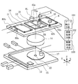
以下、本発明を図に示した実施例に基づいて詳細に説明する。図2は本発明が適用されたF2 エキシマレーザを露光光源とする投影露光装置の概略図である。
原画であるマスク13は不図示のレーザ干渉計と駆動制御手段103によって、XY方向に駆動制御されるマスクステージ16によって装置本体に支持されている。一方、感光基板であるウエハ15は、やはり不図示のレーザ干渉計と駆動制御手段103によってXY方向に駆動制御されるウエハステージ17により装置本体に支持されている。このマスク13とウエハ15は投影光学系14を介して光学的に共役な位置に置かれている。投影露光は、不図示の照明系からの露光光束が、マスク13を照明し、投影光学系14の光学倍率に比した大きさで、マスク13の光学結像像をウエハ15に投影することで行われる。
【0027】
本実施例は、走査型露光装置であり、図中Y方向に伸びるスリット状露光光がマスク13を照明し、このスリット状露光光に対してマスクステージ16とウエハステージ17の双方を、投影光学系14の光学倍率に応じた速度比でX方向に動かしてマスク13とウエハ15を走査する事によって行なわれ、マスク13上のデバイスパターン21全面を、ウエハ15上の転写領域(パターン領域)22に転写する。
【0028】
本実施例では、屈折素子のみで構成した投影光学系14を示したが、反射素子と屈折素子とを組み合わせた投影光学系であっても構わないし、本実施例のように縮小投影光学系であれ、等倍であれ、本発明の効果はなんら変わらないものである。
【0029】
マスクステージ16上には、マスク基準プレート10、11がマスク13に対して走査方向であるX方向側に固設して配置してある。一方ウエハステージ17上にはウエハ基準プレート12が固設して配置してある。
【0030】
マスク基準プレート10、11上には基準マーク50、51が形成してあり、この位置に対応した投影光学系14による転写位置に、ウエハ基準プレート12上には基準マーク60、61が形成してある。ここでマスク基準プレート10、11上の基準マーク50、51はマスク13のパターン描画面と同じ高さに配置してあり、ウエハ基準プレート12上の基準マーク60、61は、ウエハ15の露光表面と略同じ高さに配置してある。
【0031】
観察顕微鏡9L,9Rは、マスク基準プレート10、11上の基準マーク50、51や、マスク13上のパターン描画面にある物体(マーク)の観察と、ウエハ基準プレート12上の基準マーク60、61や、ウエハ15上の物体(マーク)の観察が同時に可能である様になっている。光電的に観察された像信号は、マーク検出手段101で処理され、各々の相対的位置関係情報を演算処理回路102へ送る。
【0032】
同時観察の為には、投影露光に使用されるF2 エキシマレーザ光を観察光として用いれば、投影光学系14で発生する色収差を補正する新たな光学系が不要になるので望ましい。
【0033】
今、ウエハ基準プレート12上の基準マーク60、61が、投影光学系14の下の観察顕微鏡9L、9Rによる観察位置(露光位置)へくるように、ウエハステージ17を駆動して静止する。同様にマスクステージ16を走査露光時と同じ様に走査しマスク基準プレート11上の基準マーク50、51が、観察顕微鏡9L、9Rによる観察領域内に位置するようにし静止する。
【0034】
この状態で、観察顕微鏡9L、9Rにより、基準マーク50と60、51と61のそれぞれの相対位置ずれが観察される。この相対的位置関係は、今現在投影露光されたマスク像が、ウエハステージ17上の何処に投影されているかを示している。ここでは、露光装置の光源としてF2 エキシマレーザを用いる場合について説明したが、露光装置の光源としてArFエキシマレーザを用いてもよい。
【0035】
次に、図2におけるマスク基準プレート10,11を用いたマスクステージ16上のマスク13の位置合わせについて図3を用いて説明する。
【0036】
同図に示すように、本実施例では、マスク13の位置合わせを、投影光学系14を保持する保持部材に固定基準プレート(不図示)を固設し、その固定基準プレート上に形成したマーク75a、75bで行うようにしたものである。なお、この固定基準プレートとしても本発明の基準プレートを適用することができる。
【0037】
予め、レーザ干渉計80a,bと駆動制御手段103によってX方向に駆動制御されるマスクステージ16を移動しマスク基準プレート10(あるいは11)上の基準マーク50,51(図3)を固定基準プレート上のマーク75a,75b上に移動させ、レチクルアライメント顕微鏡8により両マーク(50,51,75a,75b)の相対位置関係を計測する。そして、マスク基準プレート10(あるいは11)上の複数の位置合わせ基準マークと固定基準プレート上の複数の位置合わせマークとの相対的位置関係を検出し、マスク基準プレート10(あるいは11)上の複数の位置合わせ基準マークによって定まる座標系と固定基準プレート上の複数の位置合わせマークによって定まる座標系との関係を検出しておく。但し、固定基準プレート上のマーク75a,75bとマスク基準プレ一ト10( あるいは11)上の基準マーク50,51等の位置関係の測定は、固定基準プレート上のマーク75a,75bの位置が安定していればマスク交換の度に行う必要がない。
【0038】
マスクステージ16を移動しマスク13上のマスクアライメント用マーク42a,42bをマーク75a,75b上に位置させる。この位置近房でマスクは交換される。
【0039】
そして、レチクルアライメント顕微鏡8により両マーク(42a,42b,75a,75b)の相対位置関係を計測する。そして、マスク13上の複数の位置合わせマークと固定基準プレート上の複数の位置合わせマークとの相対的位置関係を検出して、マスク13上の複数の位置合わせマークによって定まる座標系と固定基準プレート上の複数の位置合わせマークによって定まる座標系との関係を検出し、その検出結果と予め得たマスク基準プレート10上の複数の位置合わせ基準マークによって定まる座標系と固定基準プレート上の複数の位置合わせマークによって定まる座標系との関係とを考慮して、マスクステージ16に対しマスク13を回転させる。または、マスクステージ16の走査方向をマスク13の走査すべき方向とマスクステージ16の走査方向とを一致させるように駆動制御手段103によってマスクステージ16の走査方向を制御する。
【0040】
また、固定基準プレート上のマーク75a,75bを、マスクが露光位置に位置する時のマスクステージ16上のマスクアライメント用マーク42a,42bの下に設けても上記の効果がある。
【0041】
すなわち、マスクステージを移動し基準マーク42a,42b(あるいはマーク75a,75b)をレチクルアライメント顕微鏡8の観察位置に置きマスクアライメントを行うのである。この時のマーク75a,75bと基準マーク50,51等との位置関係はマスクを搭載している状態で顕微鏡9あるいはレチクルアライメント顕微鏡8で測定することができる。この位置関係の測定も、固定基準プレート上の基準マーク75a,75bの位置が安定していればマスク交換の度に行う必要がない。
【0042】
(比較試験例)
比較例としてクロムパターン上にSiO2 膜を形成しない他は、図1(c)に示した実施例と同様の基準プレートを作成し、以下の方法で比較試験を行った。
【0043】
実施例(図1(c))および比較例として作成した基準プレートについて、ArFエキシマレーザ光(4.0mj/cm2 、1.3×10⁶ パルス)の耐久照射を行い、耐久照射前後の反射率の変化を測定した。その結果を表1に示す。
【0044】
【表1】

表1から明らかなように、比較例の基準マークでは、耐久照射により反射率の減少が見られたが、実施例の基準マークでは、照射前後で反射率の減少は認められなかった。
【0046】
このように、本発明の基準プレートによれば、ガラスあるいはSiO2 膜とクロム(またはアルミ膜)が密着しているので、照射による膜の変化が発生せず、観察像が変化しない。また、ガラス(SiO2 膜)上面に付着物がついてもコントラスト低下がなく、パターン観察が可能である。さらに、ガラスの上面に付着した物質を容易にクリーニング可能である。
【0047】
<半導体生産システムの実施例>
次に、半導体デバイス(ICやLSI等の半導体チップ、液晶パネル、CCD、薄膜磁気ヘッド、マイクロマシン等)の生産システムの例を説明する。これは半導体製造工場に設置された製造装置のトラブル対応や定期メンテナンス、あるいはソフトウェア提供などの保守サービスを、製造工場外のコンピュータネットワークを利用して行うものである。
【0048】
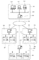
図5は全体システムをある角度から切り出して表現したものである。図中、101は半導体デバイスの製造装置を提供するベンダー(装置供給メーカ)の事業所である。製造装置の実例として、半導体製造工場で使用する各種プロセス用の半導体製造装置、例えば、前工程用機器(露光装置、レジスト処理装置、エッチング装置等のリソグラフィ装置、熱処理装置、成膜装置、平坦化装置等)や後工程用機器(組立て装置、検査装置等)を想定している。事業所101内には、製造装置の保守データベースを提供するホスト管理システム108、複数の操作端末コンピュータ110、これらを結んでイントラネットを構築するローカルエリアネットワーク(LAN)109を備える。ホスト管理システム108は、LAN109を事業所の外部ネットワークであるインタネット105に接続するためのゲートウェイと、外部からのアクセスを制限するセキュリティ機能を備える。
【0049】
一方、102〜104は、製造装置のユーザとしての半導体製造メーカの製造工場である。製造工場102〜104は、互いに異なるメーカに属する工場であっても良いし、同一のメーカに属する工場(例えば、前工程用の工場、後工程用の工場等)であっても良い。各工場102〜104内には、夫々、複数の製造装置106と、それらを結んでイントラネットを構築するローカルエリアネットワーク(LAN)111と、各製造装置106の稼動状況を監視する監視装置としてホスト管理システム107とが設けられている。各工場102〜104に設けられたホスト管理システム107は、各工場内のLAN111を工場の外部ネットワークであるインタネット105に接続するためのゲートウェイを備える。これにより各工場のLAN111からインタネット105を介してベンダー101側のホスト管理システム108にアクセスが可能となり、ホスト管理システム108のセキュリティ機能によって限られたユーザだけがアクセスが許可となっている。具体的には、インタネット105を介して、各製造装置106の稼動状況を示すステータス情報(例えば、トラブルが発生した製造装置の症状)を工場側からベンダー側に通知する他、その通知に対応する応答情報(例えば、トラブルに対する対処方法を指示する情報、対処用のソフトウェアやデータ)や、最新のソフトウェア、ヘルプ情報などの保守情報をベンダー側から受け取ることができる。各工場102〜104とベンダー101との間のデータ通信および各工場内のLAN111でのデータ通信には、インタネットで一般的に使用されている通信プロトコル(TCP/IP)が使用される。なお、工場外の外部ネットワークとしてインタネットを利用する代わりに、第三者からのアクセスができずにセキュリティの高い専用線ネットワーク(ISDNなど)を利用することもできる。
また、ホスト管理システムはベンダーが提供するものに限らずユーザがデータベースを構築して外部ネットワーク上に置き、ユーザの複数の工場から該データベースへのアクセスを許可するようにしてもよい。
【0050】
さて、図6は本実施形態の全体システムを図5とは別の角度から切り出して表現した概念図である。先の例ではそれぞれが製造装置を備えた複数のユーザ工場と、該製造装置のベンダーの管理システムとを外部ネットワークで接続して、該外部ネットワークを介して各工場の生産管理や少なくとも1台の製造装置の情報をデータ通信するものであった。これに対し本例は、複数のベンダーの製造装置を備えた工場と、該複数の製造装置のそれぞれのベンダーの管理システムとを工場外の外部ネットワークで接続して、各製造装置の保守情報をデータ通信するものである。図中、201は製造装置ユーザ(半導体デバイス製造メーカ)の製造工場であり、工場の製造ラインには各種プロセスを行う製造装置、ここでは例として露光装置202、レジスト処理装置203、成膜処理装置204が導入されている。なお図6では製造工場201は1つだけ描いているが、実際は複数の工場が同様にネットワーク化されている。工場内の各装置はLAN206で接続されてイントラネットを構成し、ホスト管理システム205で製造ラインの稼動管理がされている。一方、露光装置メーカ210、レジスト処理装置メーカ220、成膜装置メーカ230などベンダー(装置供給メーカ)の各事業所には、それぞれ供給した機器の遠隔保守を行なうためのホスト管理システム211,221,231を備え、これらは上述したように保守データベースと外部ネットワークのゲートウェイを備える。ユーザの製造工場内の各装置を管理するホスト管理システム205と、各装置のベンダーの管理システム211,221,231とは、外部ネットワーク200であるインタネットもしくは専用線ネットワークによって接続されている。このシステムにおいて、製造ラインの一連の製造機器の中のどれかにトラブルが起きると、製造ラインの稼動が休止してしまうが、トラブルが起きた機器のベンダーからインタネット200を介した遠隔保守を受けることで迅速な対応が可能で、製造ラインの休止を最小限に抑えることができる。
【0051】
半導体製造工場に設置された各製造装置はそれぞれ、ディスプレイと、ネットワークインタフェースと、記憶装置にストアされたネットワークアクセス用ソフトウェアならびに装置動作用のソフトウェアを実行するコンピュータを備える。
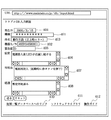
記憶装置としては内蔵メモリやハードディスク、あるいはネットワークファイルサーバーなどである。上記ネットワークアクセス用ソフトウェアは、専用又は汎用のウェブブラウザを含み、例えば図7に一例を示す様な画面のユーザインタフェースをディスプレイ上に提供する。各工場で製造装置を管理するオペレータは、画面を参照しながら、製造装置の機種(401)、シリアルナンバー(402)、トラブルの件名(403)、発生日(404)、緊急度(405)、症状(406)、対処法(407)、経過(408)等の情報を画面上の入力項目に入力する。入力された情報はインタネットを介して保守データベースに送信され、その結果の適切な保守情報が保守データベースから返信されディスプレイ上に提示される。またウェブブラウザが提供するユーザインタフェースはさらに図示のごとくハイパーリンク機能(410〜412)を実現し、オペレータは各項目の更に詳細な情報にアクセスしたり、ベンダーが提供するソフトウェアライブラリから製造装置に使用する最新バージョンのソフトウェアを引出したり、工場のオペレータの参考に供する操作ガイド(ヘルプ情報)を引出したりすることができる。
【0052】
次に上記説明した生産システムを利用した半導体デバイスの製造プロセスを説明する。図8は半導体デバイスの全体的な製造プロセスのフローを示す。ステップ1(回路設計)では半導体デバイスの回路設計を行なう。ステップ2(マスク製作)では設計した回路パターンを形成したマスクを製作する。一方、ステップ3(ウエハ製造)ではシリコン等の材料を用いてウエハを製造する。ステップ4(ウエハプロセス)は前工程と呼ばれ、上記用意したマスクとウエハを用いて、リソグラフィ技術によってウエハ上に実際の回路を形成する。次のステップ5(組み立て)は後工程と呼ばれ、ステップ4によって作製されたウエハを用いて半導体チップ化する工程であり、アッセンブリ工程(ダイシング、ボンディング)、パッケージング工程(チップ封入)等の組立て工程を含む。ステップ6(検査)ではステップ5で作製された半導体デバイスの動作確認テスト、耐久性テスト等の検査を行なう。こうした工程を経て半導体デバイスが完成し、これを出荷(ステップ7)する。前工程と後工程はそれぞれ専用の別の工場で行い、これらの工場毎に上記説明した遠隔保守システムによって保守がなされる。また前工程工場と後工程工場との間でも、インタネットまたは専用線ネットワークを介して生産管理や装置保守のための情報がデータ通信される。
【0053】
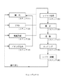
図9は上記ウエハプロセスの詳細なフローを示す。ステップ11(酸化)ではウエハの表面を酸化させる。ステップ12(CVD)ではウエハ表面に絶縁膜を成膜する。ステップ13(電極形成)ではウエハ上に電極を蒸着によって形成する。ステップ14(イオン打込み)ではウエハにイオンを打ち込む。ステップ15(レジスト処理)ではウエハに感光剤を塗布する。ステップ16(露光)では上記説明した露光装置によってマスクの回路パターンをウエハに焼付露光する。
ステップ17(現像)では露光したウエハを現像する。ステップ18(エッチング)では現像したレジスト像以外の部分を削り取る。ステップ19(レジスト剥離)ではエッチングが済んで不要となったレジストを取り除く。これらのステップを繰り返し行なうことによって、ウエハ上に多重に回路パターンを形成する。
各工程で使用する製造機器は上記説明した遠隔保守システムによって保守がなされているので、トラブルを未然に防ぐと共に、もしトラブルが発生しても迅速な復旧が可能で、従来に比べて半導体デバイスの生産性を向上させることができる。
【0054】
【発明の効果】
以上説明したように、本発明によれば、基準プレートのマークの高精度な検出を安定して行える露光装置およびデバイス製造方法を提供することができる。
【図面の簡単な説明】
【図1】本発明の基準プレートの実施例を示す模式図。
【図2】本発明の図1の基準プレートをマスク基準プレートおよびウエハ基準プレートに用いた露光装置を説明する図。
【図3】図2の露光装置におけるマスクの位置合わせを説明する図。
【図4】従来の基準プレートを示す模式図。
【図5】半導体デバイスの生産システムをある角度から見た概念図。
【図6】半導体デバイスの生産システムを別の角度から見た概念図。
【図7】ユーザーインターフェースの具体例。
【図8】デバイスの製造プロセスのフローを説明する図。
【図9】ウエハプロセスを説明する図。
【符号の説明】
1および5:ガラス基板、2:クロムパターンからなる基準マーク、3:SiO2 膜、4:付着物、8:レチクルアライメント顕微鏡、9L,9R:観察顕微鏡、10,11:マスク基準プレート、12:ウエハ基準プレート、13:マスク、14:投影光学系、15:ウエハ、16:マスクステージ、17:ウエハステージ、21:デバイスパターン、22:転写領域、42(a,b):マスクアライメント用マーク、50,51,60,61:基準マーク、75(a,b):固定基準プレート上マーク、80(a,b):レーザ干渉計、101:マーク検出手段、102:演算処理回路、103:駆動制御手段。[0001]
BACKGROUND OF THE INVENTION
The present invention relates to the EXPOSURE APPARATUS AND DEVICE MANUFACTURING METHOD.
[0002]
[Prior art]
Conventionally, a reference plate provided on a stage is used for calibration of measurement accuracy of an exposure apparatus such as baseline measurement and best focus position measurement. On the reference plate, a reference mark pattern such as chromium or aluminum film is formed on the glass for measurement in the XY direction or the Z direction. These reference mark patterns are observed with a microscope using light having the same wavelength as the exposure light.
[0003]
Further, the exposure light of the exposure apparatus tends to shorten the wavelength in order to increase the resolution of the projection optical system and expose a finer pattern.
[0004]
FIG. 4 is a view for explaining a reference plate according to the above-described prior art. In the figure, the upper part shows a schematic cross-sectional view of the reference plate, where 1 is a glass substrate, 2 is a reference mark pattern made of chromium, an aluminum film, etc., and 4 is a deposit on the surface of the reference mark pattern. The lower part shows the waveform of the observation signal.
[0005]
[Problems to be solved by the invention]
When the
[0006]
Further, as shown in FIG. 4, when the deposit 4 is attached to the pattern surface and this deposit causes a decrease in contrast, it is necessary to periodically clean the reference mark surface. If the deposit 4 is attached to the stepped portion of the pattern surface, there is a problem that cleaning is difficult.
[0007]
The present invention is to provide a can that exposure apparatus and device manufacturing method with high precision detection of the mark of the reference plate stably.
[0008]
[Means for Solving the Problems]
In order to achieve the above object, an exposure apparatus of the present invention is an exposure apparatus for exposing a wafer with a mask pattern.
A mask stage for holding the mask;
A wafer stage for holding the wafer;
A reference plate provided on the wafer stage and having a substrate and a reference mark pattern;
A microscope for observing the reference mark pattern using observation light,
The observation light is ArF excimer laser light,
The reference mark pattern is provided with chromium or aluminum as a material on a surface of the substrate on which the observation light is incident,
The exposure apparatus is characterized in that a protective film made of SiO 2 that transmits the observation light is provided in close contact with the reference mark pattern on the incident side surface.
[0019]
[Action]
With the above configuration, observation light such as ArF excimer laser light and F 2 excimer laser light is not directly applied to the reference mark pattern such as chromium and aluminum, so that damage to the reference mark pattern protective film and pattern formation film is suppressed. Can do. Moreover, even if the deposit is deposited, it adheres uniformly to the smooth surface, so that a decrease in contrast in the signal waveform of the observation image can be suppressed, and the deposit can be easily cleaned.
[0020]
【Example】
<Example of reference plate>
Each Example in the reference | standard plate of this invention is demonstrated using Fig.1 (a)-(c).
[0021]
In FIG. 1A, 1 and 5 are glass substrates, 2 is a reference mark made of a chromium pattern, and 3 is a SiO 2 film. In this example, the thickness (d) of the
[0022]
In the example shown in FIG. 1A, since the reference mark is formed on the side opposite to the observation light irradiation surface, the observation light is not directly applied to the
[0023]
In FIG.1 (b), 5 is the glass substrate similar to the
In the example shown in FIG. 1B, since the substrate 5 is laminated on the reference mark, the observation light is not directly applied to the
[0024]
In FIG. 1C, 3 is a protective film made of SiO 2 , and the thickness (d) from the
[0025]
<Example of exposure apparatus>
Next, an exposure apparatus using the reference plate of this embodiment as a mask reference plate and a wafer reference plate will be described with reference to FIGS.
[0026]
Hereinafter, the present invention will be described in detail based on the embodiments shown in the drawings. FIG. 2 is a schematic view of a projection exposure apparatus using an F 2 excimer laser to which the present invention is applied as an exposure light source.
The
[0027]
The present embodiment is a scanning exposure apparatus, and slit-like exposure light extending in the Y direction in the drawing illuminates the
[0028]
In the present embodiment, the projection
[0029]
On the
[0030]
Reference marks 50 and 51 are formed on the
[0031]
The
[0032]
For simultaneous observation, it is desirable to use F 2 excimer laser light used for projection exposure as observation light because a new optical system for correcting chromatic aberration generated in the projection
[0033]
Now, the
[0034]
In this state, the relative positional shifts of the reference marks 50 and 60 and 51 and 61 are observed by the
[0035]
Next, the alignment of the
[0036]
As shown in the figure, in this embodiment, the
[0037]
The
[0038]
The
[0039]
Then, the relative positional relationship between the marks (42a, 42b, 75a, 75b) is measured by the reticle alignment microscope 8. Then, the relative positional relationship between the plurality of alignment marks on the
[0040]
Further, the above-described effects can be obtained by providing the
[0041]
That is, the mask stage is moved, and the reference marks 42a and 42b (or marks 75a and 75b) are placed at the observation position of the reticle alignment microscope 8 to perform mask alignment. The positional relationship between the
[0042]
(Comparative test example)
As a comparative example, a reference plate similar to the example shown in FIG. 1C was prepared except that the SiO 2 film was not formed on the chromium pattern, and a comparative test was performed by the following method.
[0043]
The reference plate prepared as an example (FIG. 1C) and a comparative example was subjected to durable irradiation with ArF excimer laser light (4.0 mj / cm 2 , 1.3 × 10 6 pulses), and reflection before and after the durable irradiation. The change in rate was measured. The results are shown in Table 1.
[0044]
[Table 1]
As is clear from Table 1, in the reference mark of the comparative example, a decrease in reflectance was observed due to durable irradiation, but in the reference mark of the example, no decrease in reflectance was observed before and after irradiation.
[0046]
As described above, according to the reference plate of the present invention, since the glass or SiO 2 film is in close contact with the chromium (or aluminum film), the film does not change due to irradiation, and the observation image does not change. Further, even if an adherent is attached to the upper surface of the glass (SiO 2 film), the contrast is not lowered and pattern observation is possible. Furthermore, the substance adhering to the upper surface of the glass can be easily cleaned.
[0047]
<Example of semiconductor production system>
Next, an example of a production system for semiconductor devices (semiconductor chips such as IC and LSI, liquid crystal panels, CCDs, thin film magnetic heads, micromachines, etc.) will be described. In this method, maintenance services such as troubleshooting, periodic maintenance, and software provision for manufacturing apparatuses installed in a semiconductor manufacturing factory are performed using a computer network outside the manufacturing factory.
[0048]
FIG. 5 shows the whole system cut out from a certain angle. In the figure,
[0049]
On the other hand, 102 to 104 are manufacturing factories of semiconductor manufacturers as users of manufacturing apparatuses. The
The host management system is not limited to the one provided by the vendor, and the user may construct a database and place it on an external network, and allow access to the database from a plurality of user factories.
[0050]
FIG. 6 is a conceptual diagram showing the overall system of the present embodiment cut out from an angle different from that in FIG. In the previous example, a plurality of user factories each equipped with a manufacturing apparatus and a management system of a vendor of the manufacturing apparatus are connected via an external network, and production management of each factory or at least one unit is performed via the external network. Data communication of manufacturing equipment was performed. On the other hand, in this example, a factory equipped with a plurality of vendors' manufacturing devices and a management system of each vendor of the plurality of manufacturing devices are connected via an external network outside the plant, and maintenance information for each manufacturing device is obtained. Data communication. In the figure,
[0051]
Each manufacturing apparatus installed in the semiconductor manufacturing factory includes a display, a network interface, and a computer that executes network access software stored in a storage device and software for operating the apparatus.
The storage device is a built-in memory, a hard disk, or a network file server. The network access software includes a dedicated or general-purpose web browser, and provides, for example, a user interface having a screen as shown in FIG. 7 on the display. The operator who manages the manufacturing apparatus in each factory refers to the screen while referring to the screen of the manufacturing apparatus (401), serial number (402), trouble subject (403), date of occurrence (404), urgency (405), Information such as symptom (406), coping method (407), progress (408), etc. is input to the input items on the screen. The input information is transmitted to the maintenance database via the Internet, and appropriate maintenance information as a result is returned from the maintenance database and presented on the display. The user interface provided by the web browser further realizes a hyperlink function (410 to 412) as shown in the figure, and the operator can access more detailed information on each item or use it from the software library provided by the vendor to the manufacturing apparatus. The latest version of software can be pulled out, and operation guides (help information) can be pulled out for reference by factory operators.
[0052]
Next, a semiconductor device manufacturing process using the production system described above will be described. FIG. 8 shows the flow of the entire manufacturing process of the semiconductor device. In step 1 (circuit design), a semiconductor device circuit is designed. In step 2 (mask production), a mask on which the designed circuit pattern is formed is produced. On the other hand, in step 3 (wafer manufacture), a wafer is manufactured using a material such as silicon. Step 4 (wafer process) is called a pre-process, and an actual circuit is formed on the wafer by lithography using the prepared mask and wafer. The next step 5 (assembly) is called a post-process, and is a process for forming a semiconductor chip using the wafer produced in step 4, and is an assembly process (dicing, bonding), packaging process (chip encapsulation), etc. Process. In step 6 (inspection), inspections such as an operation confirmation test and a durability test of the semiconductor device manufactured in step 5 are performed. Through these steps, the semiconductor device is completed and shipped (step 7). The pre-process and post-process are performed in separate dedicated factories, and maintenance is performed for each of these factories by the remote maintenance system described above. In addition, information for production management and apparatus maintenance is communicated between the pre-process factory and the post-process factory via the Internet or a dedicated line network.
[0053]
FIG. 9 shows a detailed flow of the wafer process. In step 11 (oxidation), the wafer surface is oxidized. In step 12 (CVD), an insulating film is formed on the wafer surface. In step 13 (electrode formation), an electrode is formed on the wafer by vapor deposition. In step 14 (ion implantation), ions are implanted into the wafer. In step 15 (resist process), a photosensitive agent is applied to the wafer. In step 16 (exposure), the circuit pattern of the mask is printed onto the wafer by exposure using the exposure apparatus described above.
In step 17 (development), the exposed wafer is developed. In step 18 (etching), portions other than the developed resist image are removed. In step 19 (resist stripping), unnecessary resist after etching is removed. By repeating these steps, multiple circuit patterns are formed on the wafer.
Since the manufacturing equipment used in each process is maintained by the remote maintenance system described above, it is possible to prevent problems before they occur, and to recover quickly if a problem occurs. Productivity can be improved.
[0054]
【The invention's effect】
As described above, according to the present invention, a highly accurate detection of the mark of the reference plate can provide a stable line obtain exposure apparatus and device manufacturing method.
[Brief description of the drawings]
FIG. 1 is a schematic view showing an embodiment of a reference plate of the present invention.
FIG. 2 is a view for explaining an exposure apparatus using the reference plate of FIG. 1 of the present invention as a mask reference plate and a wafer reference plate;
FIG. 3 is a view for explaining mask alignment in the exposure apparatus of FIG. 2;
FIG. 4 is a schematic diagram showing a conventional reference plate.
FIG. 5 is a conceptual diagram of a semiconductor device production system as viewed from a certain angle.
FIG. 6 is a conceptual diagram of a semiconductor device production system viewed from another angle.
FIG. 7 shows a specific example of a user interface.
FIG. 8 is a diagram for explaining a flow of a device manufacturing process.
FIG. 9 is a diagram illustrating a wafer process.
[Explanation of symbols]
1 and 5: glass substrate, 2: fiducial mark made of chrome pattern, 3: SiO 2 film, 4: deposit, 8: reticle alignment microscope, 9L, 9R: observation microscope, 10, 11: mask reference plate, 12: Wafer reference plate, 13: mask, 14: projection optical system, 15: wafer, 16: mask stage, 17: wafer stage, 21: device pattern, 22: transfer area, 42 (a, b): mark for mask alignment, 50, 51, 60, 61: reference mark, 75 (a, b): mark on fixed reference plate, 80 (a, b): laser interferometer, 101: mark detection means, 102: arithmetic processing circuit, 103: drive Control means.
Claims (3)
前記マスクを保持するマスクステージと、
前記ウエハを保持するウエハステージと、
前記ウエハステージ上に設けられており、基板と基準マークパターンとを有する基準プレートと、
観察光を用いて前記基準マークパターンを観察する顕微鏡と、を備え、
前記観察光は、ArFエキシマレーザ光であり、
前記基準マークパターンは、前記基板の前記観察光が入射する側の面にクロムまたはアルミニウムをその材質として設けられており、
該入射する側の面の前記基準マークパターン上に、前記観察光を透過するSiO2からなる保護膜が密着させて設けられている
ことを特徴とする露光装置。In an exposure apparatus that exposes a wafer with a mask pattern,
A mask stage for holding the mask;
A wafer stage for holding the wafer;
A reference plate provided on the wafer stage and having a substrate and a reference mark pattern;
A microscope for observing the reference mark pattern using observation light,
The observation light is ArF excimer laser light,
The reference mark pattern is provided with chromium or aluminum as its material on the surface of the substrate on which the observation light is incident,
An exposure apparatus, wherein a protective film made of SiO 2 that transmits the observation light is provided in close contact with the reference mark pattern on the incident side surface.
nd=λ/2×m(m=1,2,3・・・)
を満足する厚さdの近傍である
ことを特徴とする請求項1に記載の露光装置。The thickness of the protective film is such that the refractive index of SiO 2 with respect to the observation light is n, and the wavelength of the observation light is λ.
nd = λ / 2 × m (m = 1, 2, 3,...)
The exposure apparatus according to claim 1, wherein the exposure apparatus is in the vicinity of a thickness d that satisfies the following.
Priority Applications (4)
| Application Number | Priority Date | Filing Date | Title |
|---|---|---|---|
| JP2000183410A JP4579376B2 (en) | 2000-06-19 | 2000-06-19 | Exposure apparatus and device manufacturing method |
| US09/881,804 US6608666B2 (en) | 2000-06-19 | 2001-06-18 | Reference plate, exposure apparatus, device manufacturing system, device manufacturing method, semiconductor manufacturing factory, and exposure apparatus maintenance method |
| DE60138509T DE60138509D1 (en) | 2000-06-19 | 2001-06-18 | Reference plate for an exposure apparatus |
| EP01305290A EP1168085B1 (en) | 2000-06-19 | 2001-06-18 | Reference plate for exposure apparatus |
Applications Claiming Priority (1)
| Application Number | Priority Date | Filing Date | Title |
|---|---|---|---|
| JP2000183410A JP4579376B2 (en) | 2000-06-19 | 2000-06-19 | Exposure apparatus and device manufacturing method |
Publications (3)
| Publication Number | Publication Date |
|---|---|
| JP2002008962A JP2002008962A (en) | 2002-01-11 |
| JP2002008962A5 JP2002008962A5 (en) | 2007-08-02 |
| JP4579376B2 true JP4579376B2 (en) | 2010-11-10 |
Family
ID=18684001
Family Applications (1)
| Application Number | Title | Priority Date | Filing Date |
|---|---|---|---|
| JP2000183410A Expired - Fee Related JP4579376B2 (en) | 2000-06-19 | 2000-06-19 | Exposure apparatus and device manufacturing method |
Country Status (4)
| Country | Link |
|---|---|
| US (1) | US6608666B2 (en) |
| EP (1) | EP1168085B1 (en) |
| JP (1) | JP4579376B2 (en) |
| DE (1) | DE60138509D1 (en) |
Families Citing this family (16)
| Publication number | Priority date | Publication date | Assignee | Title |
|---|---|---|---|---|
| US20040071161A1 (en) * | 2000-06-30 | 2004-04-15 | Tokyo Electron Limited | Part maintenance system and part maintenance method of semiconductor processing system |
| US7095484B1 (en) * | 2001-06-27 | 2006-08-22 | University Of South Florida | Method and apparatus for maskless photolithography |
| EP2017675A1 (en) * | 2001-07-09 | 2009-01-21 | Canon Kabushiki Kaisha | Exposure apparatus |
| JP2004206702A (en) * | 2002-12-12 | 2004-07-22 | Tokyo Electron Ltd | Parts management system, its method, program, and storage medium |
| JP4101076B2 (en) * | 2003-02-06 | 2008-06-11 | キヤノン株式会社 | Position detection method and apparatus |
| TW201738932A (en) | 2003-10-09 | 2017-11-01 | Nippon Kogaku Kk | Exposure apparatus, exposure method, and device producing method |
| US20060000814A1 (en) * | 2004-06-30 | 2006-01-05 | Bo Gu | Laser-based method and system for processing targeted surface material and article produced thereby |
| JP2006173377A (en) * | 2004-12-16 | 2006-06-29 | Nikon Corp | Optical part and projection aligner |
| JP4923480B2 (en) * | 2005-08-23 | 2012-04-25 | 株式会社ニコン | Exposure apparatus, device manufacturing method, and measurement member |
| KR101435124B1 (en) * | 2008-04-29 | 2014-08-29 | 삼성전자 주식회사 | Calibration method for exposure device, exposure method for photoresist layer using the same and exposure device for performing the exposure method |
| NL2002998A1 (en) * | 2008-06-18 | 2009-12-22 | Asml Netherlands Bv | Lithographic apparatus. |
| NL2003529A (en) * | 2008-10-24 | 2010-04-27 | Asml Netherlands Bv | Lithographic apparatus, device manufacturing method and position control method. |
| JP5355245B2 (en) * | 2009-06-25 | 2013-11-27 | 株式会社日立ハイテクノロジーズ | Exposure apparatus, exposure method, and manufacturing method of display panel substrate |
| CN104272427B (en) * | 2012-03-08 | 2017-05-17 | 迈普尔平版印刷Ip有限公司 | Charged particle lithography system with alignment sensor and beam measurement sensor |
| JP6219320B2 (en) | 2012-03-08 | 2017-10-25 | マッパー・リソグラフィー・アイピー・ビー.ブイ. | Lithographic system and method for processing a target such as a wafer |
| JP7089348B2 (en) * | 2017-07-28 | 2022-06-22 | キヤノン株式会社 | Imprint device, imprint method and article manufacturing method |
Citations (3)
| Publication number | Priority date | Publication date | Assignee | Title |
|---|---|---|---|---|
| JPH0325913A (en) * | 1989-06-23 | 1991-02-04 | Nec Kyushu Ltd | Reduction projection type exposure device |
| JPH0437113A (en) * | 1990-06-01 | 1992-02-07 | Mitsubishi Electric Corp | Contraction projecting aligner |
| JPH04155813A (en) * | 1990-10-19 | 1992-05-28 | Nec Corp | Alignment mark |
Family Cites Families (24)
| Publication number | Priority date | Publication date | Assignee | Title |
|---|---|---|---|---|
| NL301413A (en) * | 1963-12-05 | |||
| JPS57119348A (en) * | 1981-01-17 | 1982-07-24 | Mitsubishi Electric Corp | Hard mask |
| JPS58214154A (en) * | 1982-06-08 | 1983-12-13 | Nec Corp | Photomask |
| US5200798A (en) * | 1990-07-23 | 1993-04-06 | Hitachi, Ltd. | Method of position detection and the method and apparatus of printing patterns by use of the position detection method |
| US5477309A (en) * | 1992-03-09 | 1995-12-19 | Nikon Corporation | Alignment apparatus |
| JP3420314B2 (en) | 1993-12-03 | 2003-06-23 | キヤノン株式会社 | Position shift measuring method and measuring device using the same |
| JPH07249558A (en) * | 1994-03-09 | 1995-09-26 | Nikon Corp | Alignment method |
| JP3555230B2 (en) * | 1994-05-18 | 2004-08-18 | 株式会社ニコン | Projection exposure equipment |
| US6018384A (en) * | 1994-09-07 | 2000-01-25 | Nikon Corporation | Projection exposure system |
| JP3555208B2 (en) * | 1994-12-14 | 2004-08-18 | 株式会社ニコン | Exposure method |
| US5751404A (en) * | 1995-07-24 | 1998-05-12 | Canon Kabushiki Kaisha | Exposure apparatus and method wherein alignment is carried out by comparing marks which are incident on both reticle stage and wafer stage reference plates |
| JP3437352B2 (en) | 1995-10-02 | 2003-08-18 | キヤノン株式会社 | Illumination optical system and light source device |
| US6242792B1 (en) * | 1996-07-02 | 2001-06-05 | Denso Corporation | Semiconductor device having oblique portion as reflection |
| JP3428829B2 (en) | 1996-08-27 | 2003-07-22 | キヤノン株式会社 | Positioning method and projection exposure apparatus using the same |
| KR100197885B1 (en) * | 1996-12-23 | 1999-06-15 | 윤종용 | Device for protecting base mark of exposure apparatus |
| JPH10284412A (en) * | 1997-04-10 | 1998-10-23 | Nikon Corp | Stage device for light transfer with outside and projection aligner |
| US5981352A (en) * | 1997-09-08 | 1999-11-09 | Lsi Logic Corporation | Consistent alignment mark profiles on semiconductor wafers using fine grain tungsten protective layer |
| US5985764A (en) * | 1997-12-22 | 1999-11-16 | Taiwan Semiconductor Manufacturing Company, Ltd. | Layer independent alignment system |
| JP3090113B2 (en) * | 1998-02-13 | 2000-09-18 | 日本電気株式会社 | Method for manufacturing semiconductor device |
| US6197481B1 (en) * | 1998-09-17 | 2001-03-06 | Taiwan Semiconductor Manufacturing Company | Wafer alignment marks protected by photoresist |
| US6294018B1 (en) * | 1999-09-15 | 2001-09-25 | Lucent Technologies | Alignment techniques for epitaxial growth processes |
| US6057206A (en) * | 1999-10-01 | 2000-05-02 | Advanced Micro Devices, Inc. | Mark protection scheme with no masking |
| US6417076B1 (en) * | 2000-06-05 | 2002-07-09 | Micron Technology, Inc. | Automated combi deposition apparatus and method |
| TW497204B (en) * | 2001-02-08 | 2002-08-01 | Mosel Vitelic Inc | Method for protecting alignment mark of stepping machine |
-
2000
- 2000-06-19 JP JP2000183410A patent/JP4579376B2/en not_active Expired - Fee Related
-
2001
- 2001-06-18 DE DE60138509T patent/DE60138509D1/en not_active Expired - Lifetime
- 2001-06-18 EP EP01305290A patent/EP1168085B1/en not_active Expired - Lifetime
- 2001-06-18 US US09/881,804 patent/US6608666B2/en not_active Expired - Fee Related
Patent Citations (3)
| Publication number | Priority date | Publication date | Assignee | Title |
|---|---|---|---|---|
| JPH0325913A (en) * | 1989-06-23 | 1991-02-04 | Nec Kyushu Ltd | Reduction projection type exposure device |
| JPH0437113A (en) * | 1990-06-01 | 1992-02-07 | Mitsubishi Electric Corp | Contraction projecting aligner |
| JPH04155813A (en) * | 1990-10-19 | 1992-05-28 | Nec Corp | Alignment mark |
Also Published As
| Publication number | Publication date |
|---|---|
| EP1168085A2 (en) | 2002-01-02 |
| EP1168085A3 (en) | 2005-12-07 |
| US20020067473A1 (en) | 2002-06-06 |
| DE60138509D1 (en) | 2009-06-10 |
| US6608666B2 (en) | 2003-08-19 |
| JP2002008962A (en) | 2002-01-11 |
| EP1168085B1 (en) | 2009-04-29 |
Similar Documents
| Publication | Publication Date | Title |
|---|---|---|
| JP4579376B2 (en) | Exposure apparatus and device manufacturing method | |
| US7247868B2 (en) | Position detection method and apparatus | |
| US6559924B2 (en) | Alignment method, alignment apparatus, profiler, exposure apparatus, exposure apparatus maintenance method, semiconductor device manufacturing method, and semiconductor manufacturing factory | |
| JP2002280283A (en) | Substrate treating device | |
| JP4616983B2 (en) | Position detection apparatus, projection exposure apparatus using the detection apparatus, and device manufacturing method | |
| JP2003028673A (en) | Optical encoder, semiconductor manufacturing apparatus, device manufacturing method, semiconductor manufacturing plant and maintaining method for semiconductor manufacturing apparatus | |
| JP4798891B2 (en) | Exposure apparatus and device manufacturing method | |
| JP4666747B2 (en) | Exposure apparatus and device manufacturing method | |
| US6876435B2 (en) | Exposure method, plane alignment method, exposure apparatus, and device manufacturing method | |
| JP4227324B2 (en) | Exposure equipment | |
| US6646714B2 (en) | Exposure apparatus, imaging performance measurement method, device manufacturing method, semiconductor manufacturing factory, and exposure apparatus maintenance method | |
| JP2003234265A (en) | Exposure device | |
| JP2001297961A (en) | Projection aligner | |
| JP4817545B2 (en) | Exposure apparatus and device manufacturing method | |
| JP4154197B2 (en) | Position detection method, position detection apparatus, and exposure apparatus | |
| JP2003142365A (en) | Apparatus and method for exposure | |
| JP5121096B2 (en) | Focus position detection method, focus position detection apparatus, and exposure apparatus | |
| JP2002083761A (en) | Aligner and exposure method | |
| JP2002203773A (en) | Aligner | |
| JP4881484B2 (en) | Exposure apparatus and device manufacturing method | |
| JP2003022948A (en) | Projection aligner | |
| JP3880355B2 (en) | Scanning exposure equipment | |
| JP2002373848A (en) | Method and device for measuring surface state of substrate holder | |
| JP2003007609A (en) | Reticle holder, reticle transfer device, and method and system for exposure | |
| JP2002151377A (en) | Projection aligner, projection aligning method, device- manufacturing method, and maintenance method for semiconductor manufacturing factory, and the projection aligner |
Legal Events
| Date | Code | Title | Description |
|---|---|---|---|
| A521 | Written amendment |
Free format text: JAPANESE INTERMEDIATE CODE: A523 Effective date: 20070619 |
|
| A621 | Written request for application examination |
Free format text: JAPANESE INTERMEDIATE CODE: A621 Effective date: 20070619 |
|
| RD01 | Notification of change of attorney |
Free format text: JAPANESE INTERMEDIATE CODE: A7421 Effective date: 20090406 |
|
| A977 | Report on retrieval |
Free format text: JAPANESE INTERMEDIATE CODE: A971007 Effective date: 20091106 |
|
| A131 | Notification of reasons for refusal |
Free format text: JAPANESE INTERMEDIATE CODE: A131 Effective date: 20091117 |
|
| A521 | Written amendment |
Free format text: JAPANESE INTERMEDIATE CODE: A523 Effective date: 20091225 |
|
| RD04 | Notification of resignation of power of attorney |
Free format text: JAPANESE INTERMEDIATE CODE: A7424 Effective date: 20100201 |
|
| A131 | Notification of reasons for refusal |
Free format text: JAPANESE INTERMEDIATE CODE: A131 Effective date: 20100615 |
|
| RD01 | Notification of change of attorney |
Free format text: JAPANESE INTERMEDIATE CODE: A7421 Effective date: 20100630 |
|
| A521 | Written amendment |
Free format text: JAPANESE INTERMEDIATE CODE: A523 Effective date: 20100728 |
|
| TRDD | Decision of grant or rejection written | ||
| A01 | Written decision to grant a patent or to grant a registration (utility model) |
Free format text: JAPANESE INTERMEDIATE CODE: A01 Effective date: 20100824 |
|
| A01 | Written decision to grant a patent or to grant a registration (utility model) |
Free format text: JAPANESE INTERMEDIATE CODE: A01 |
|
| A61 | First payment of annual fees (during grant procedure) |
Free format text: JAPANESE INTERMEDIATE CODE: A61 Effective date: 20100826 |
|
| FPAY | Renewal fee payment (event date is renewal date of database) |
Free format text: PAYMENT UNTIL: 20130903 Year of fee payment: 3 |
|
| R150 | Certificate of patent or registration of utility model |
Free format text: JAPANESE INTERMEDIATE CODE: R150 |
|
| LAPS | Cancellation because of no payment of annual fees |