JP4562371B2 - Manufacturing method of semiconductor device - Google Patents
Manufacturing method of semiconductor device Download PDFInfo
- Publication number
- JP4562371B2 JP4562371B2 JP2003356195A JP2003356195A JP4562371B2 JP 4562371 B2 JP4562371 B2 JP 4562371B2 JP 2003356195 A JP2003356195 A JP 2003356195A JP 2003356195 A JP2003356195 A JP 2003356195A JP 4562371 B2 JP4562371 B2 JP 4562371B2
- Authority
- JP
- Japan
- Prior art keywords
- wiring
- forming
- semiconductor device
- manufacturing
- support substrate
- Prior art date
- Legal status (The legal status is an assumption and is not a legal conclusion. Google has not performed a legal analysis and makes no representation as to the accuracy of the status listed.)
- Expired - Fee Related
Links
Images


Landscapes
- Encapsulation Of And Coatings For Semiconductor Or Solid State Devices (AREA)
Description
本発明は、ボール状の導電端子を有するBGA(Ball Grip Array)型の半導体装置の製造方法に関するものである。 The present invention relates to a method for manufacturing a BGA (Ball Grip Array) type semiconductor device having ball-shaped conductive terminals.
近年、三次元実装技術として、また新たなパッケージ技術として、CSP(Chip Size Package)が注目されている。CSPとは、半導体チップの外形寸法と略同サイズの外形寸法を有する小型パッケージをいう。 In recent years, CSP (Chip Size Package) has attracted attention as a three-dimensional mounting technique and as a new packaging technique. The CSP refers to a small package having an outer dimension substantially the same as the outer dimension of a semiconductor chip.
従来より、CSPの一種として、BGA型の半導体装置が知られている。このBGA型の半導体装置は、半田等の金属部材からなるボール状の導電端子をパッケージの一主面上に格子状に複数配列し、パッケージの他の面上に搭載される半導体チップと電気的に接続したものである。 Conventionally, a BGA type semiconductor device is known as a kind of CSP. In this BGA type semiconductor device, a plurality of ball-shaped conductive terminals made of a metal member such as solder are arranged in a lattice pattern on one main surface of a package, and electrically connected to a semiconductor chip mounted on the other surface of the package. Is connected to.
そして、このBGA型の半導体装置を電子機器に組み込む際には、各導電端子をプリント基板上の配線パターンに圧着することで、半導体チップとプリント基板上に搭載される外部回路とを電気的に接続している。 When incorporating this BGA type semiconductor device into an electronic device, each conductive terminal is crimped to a wiring pattern on the printed circuit board, thereby electrically connecting the semiconductor chip and the external circuit mounted on the printed circuit board. Connected.
このようなBGA型の半導体装置は、側部に突出したリードピンを有するSOP(Small Outline Package)やQFP(Quad Flat Package)等の他のCSP型の半導体装置に比べて、多数の導電端子を設けることが出来、しかも小型化できるという長所を有する。このBGA型の半導体装置は、例えば携帯電話機に搭載されるデジタルカメラのイメージセンサチップとしての用途がある。 Such a BGA type semiconductor device is provided with a larger number of conductive terminals than other CSP type semiconductor devices such as SOP (Small Outline Package) and QFP (Quad Flat Package) having lead pins protruding from the side. It has the advantage that it can be reduced in size. This BGA type semiconductor device has an application as an image sensor chip of a digital camera mounted on a mobile phone, for example.
図11は、従来のBGA型の半導体装置の概略構成を成すものであり、図11(A)は、このBGA型の半導体装置の表面側の斜視図である。また、図11(B)はこのBGA型の半導体装置の裏面側の斜視図である。 FIG. 11 shows a schematic configuration of a conventional BGA type semiconductor device, and FIG. 11A is a perspective view of the surface side of the BGA type semiconductor device. FIG. 11B is a perspective view of the back side of the BGA type semiconductor device.
このBGA型の半導体装置101は、第1及び第2のガラス基板102、103の間に半導体チップ104がエポキシ樹脂105a、105bを介して封止されている。第2のガラス基板103の一主面上、即ちBGA型の半導体装置101の裏面上には、導電端子106が格子状に複数配置されている。この導電端子106は、第2の配線110を介して半導体チップ104へと接続される。複数の第2の配線110には、それぞれ半導体チップ104の内部から引き出されたアルミニウム配線が接続されており、各導電端子106と半導体チップ104との電気的接続がなされている。
In this BGA type semiconductor device 101, a semiconductor chip 104 is sealed between first and second glass substrates 102 and 103 via epoxy resins 105a and 105b. A plurality of
このBGA型の半導体装置101の断面構造について図12を参照して更に詳しく説明する。図12はダイシングラインに沿って、個々のチップに分割されたBGA型の半導体装置101の断面図を示している。 A cross-sectional structure of the BGA type semiconductor device 101 will be described in more detail with reference to FIG. FIG. 12 shows a cross-sectional view of the BGA type semiconductor device 101 divided into individual chips along the dicing line.
半導体チップ104の表面に配置された絶縁膜108上に第1の配線107が設けられている。この半導体チップ104は樹脂105aによって第1のガラス基板102と接着されている。また、この半導体チップ104の裏面は、樹脂105bによって第2のガラス基板103と接着されている。
A
そして、第1の配線107の一端は第2の配線110と接続されている。この第2の配線110は、第1の配線107の一端から第2のガラス基板103の表面に延在している。そして、第2のガラス基板103上に延在した第2の配線上には、ボール状の導電端子106が形成されている。
One end of the
上述した技術は、例えば以下の特許文献1に記載されている。
上述したBGA型の半導体装置101は、上記ダイシング工程前に有機系樹脂を用いて、V字型の溝VGを有した半導体装置の表面に保護膜111を形成している(図13参照)。当該保護膜111を形成する方法として、半導体チップ104の裏面側を上に向けて、熱硬化性の有機系樹脂を上方からポッディング(滴下)して、半導体ウエハ自体を回転させることで、その遠心力を利用して、第2の配線110の表面に保護膜111を形成する方法をとってきた。
In the BGA type semiconductor device 101 described above, the protective film 111 is formed on the surface of the semiconductor device having the V-shaped groove VG using an organic resin before the dicing step (see FIG. 13). As a method of forming the protective film 111, the semiconductor wafer 104 is rotated by podding (dropping) a thermosetting organic resin from above with the back side of the semiconductor chip 104 facing upward. A method has been adopted in which the protective film 111 is formed on the surface of the
しかし、この方法では図13(A)に示すようにダイシングライン(図中破線)のV字型の溝VGの底部に当該熱硬化性の有機系樹脂が必要以上に厚く溜まる。これは、当該有機系樹脂が粘性のあるペーストの性質を有するためである。このため、当該保護膜111をベーキング(加熱処理)によって熱硬化させると、V字型の溝VGに溜まった有機系樹脂が、半導体装置101の他の部分を覆う有機系樹脂に比べてより大きく収縮する。その結果、V字型の溝VGでより大きな収縮が生じて、半導体ウエハが反ってしまうという問題点があった(図13(B)の矢印方向に反りが生じる)。 However, in this method, as shown in FIG. 13A, the thermosetting organic resin accumulates thicker than necessary at the bottom of the V-shaped groove VG of the dicing line (broken line in the figure). This is because the organic resin has a viscous paste property. Therefore, when the protective film 111 is thermally cured by baking (heat treatment), the organic resin accumulated in the V-shaped groove VG is larger than the organic resin that covers the other part of the semiconductor device 101. Shrink. As a result, there is a problem that the V-shaped groove VG is further contracted and the semiconductor wafer is warped (warping occurs in the direction of the arrow in FIG. 13B).
このような反りがある半導体ウエハでは、その後の製造工程に支障を招いていた。特に、上記保護膜111をマスクとしたスクリーン印刷により、導電端子106を形成する工程において、印刷位置合わせの精度が悪くなり、BGA型の半導体装置101の歩留まりや信頼性に問題が生じるおそれがあった。
A semiconductor wafer having such a warp has hindered subsequent manufacturing processes. In particular, in the process of forming the
本発明は、以上の欠点に鑑み成されたものであり、BGA型の半導体装置101の製造工程中に生じる半導体ウエハの反りを解消し、半導体装置の信頼性を向上させるものである。 The present invention has been made in view of the above drawbacks, and eliminates the warpage of the semiconductor wafer that occurs during the manufacturing process of the BGA type semiconductor device 101 and improves the reliability of the semiconductor device.
本発明は、導電端子に加わる力を吸収する緩衝部材または保護膜または当該保護膜に開口部を設けるためのレジスト層をスプレーコートにより形成することにより、その膜厚を均一とし、半導体ウエハの反りを防止したものである。これにより、その後に行われるスクリーン印刷において、導電端子の形成位置合わせの精度が高まり、BGA型の半導体装置の歩留まり及び信頼性を向上させることができる。 In the present invention, a buffer member or a protective film that absorbs a force applied to a conductive terminal, or a resist layer for providing an opening in the protective film is formed by spray coating, thereby making the film thickness uniform and warping the semiconductor wafer. It is what prevented. Thus, in the subsequent screen printing, the accuracy of forming the conductive terminals is increased, and the yield and reliability of the BGA type semiconductor device can be improved.
本発明によれば、緩衝部材または保護膜またはレジスト層の各層を形成する際に、成膜材料を霧状の微粒子にして噴出させコーティングするスプレーコートを用いているので、上記各層が均一の膜厚となるように形成される。そして、保護膜やレジスト層のベーキングの際に、保護膜やレジスト層が局所的に大きく収縮することが抑制されるので、半導体ウエハの反りを防止することができる。これにより、スクリーン印刷のように、半導体ウエハの平坦性が問題となる工程の精度を向上させることができ、BGA型の半導体装置の歩留まりや信頼性を向上できる。 According to the present invention, when each layer of the buffer member, the protective film, or the resist layer is formed, the film forming material is sprayed as mist-like fine particles and spray coating is used. It is formed to be thick. Further, when the protective film or the resist layer is baked, the local contraction of the protective film or the resist layer is largely suppressed, so that the warp of the semiconductor wafer can be prevented. Thus, the accuracy of a process in which flatness of a semiconductor wafer is a problem as in screen printing can be improved, and the yield and reliability of a BGA type semiconductor device can be improved.
以下、本発明を実施するための最良の形態(以下、「実施形態」と略称する)に係る半導体装置の製造方法について図面を参照しながら説明する。図1乃至図6は、本実施形態に係る半導体装置の製造方法を説明する断面図である。 A method for manufacturing a semiconductor device according to the best mode for carrying out the present invention (hereinafter abbreviated as “embodiment”) will be described below with reference to the drawings. 1 to 6 are cross-sectional views illustrating a method for manufacturing a semiconductor device according to this embodiment.
まず、図1に示すように、複数の半導体チップ1を有する半導体ウエハ1aを用意する。これらの半導体チップ1は、例えばCCDのイメージセンサ用のチップであり、半導体のウエハープロセスにより形成される。半導体ウエハ1a上には絶縁膜2が形成されており、この絶縁膜上に、アルミニウムまたは銅を主体とする一対の第1の配線3をスパッタ法により約1μmの厚さに形成する。
First, as shown in FIG. 1, a semiconductor wafer 1a having a plurality of semiconductor chips 1 is prepared. These semiconductor chips 1 are, for example, chips for CCD image sensors, and are formed by a semiconductor wafer process. An insulating film 2 is formed on the semiconductor wafer 1a, and a pair of
一対の第1の配線3は、半導体チップ1毎に分断するための境界ラインS(ダイシングラインまたはスクライブラインと呼ばれる)の両側に対向して形成する。尚、境界ラインSを跨るように第1の配線3を形成し、その後、一対の第1の配線3となるように分断してもよい。
The pair of
ここで、一対の第1の配線3は、半導体チップ1のボンディングパッドから、境界ラインSまで拡張されたパッドである。すなわち、一対の第1の配線3は外部接続パッドであって、半導体チップ1の図示しない回路と電気的に接続されている。
Here, the pair of
次に、図2に示すように、第1の配線3が形成された半導体ウエハ1aの表面上に、約200μmの膜厚を有する第1のガラス基板4を透明のエポキシ材料からなる樹脂5aを接着剤として用いて貼り合わせる。そして、半導体ウエハ1aをバックグラインドしてチップ厚を約100μmとした後、当該半導体ウエハ1aをその裏面側から境界ラインSに沿ってドライエッチングし、絶縁膜2を露出させる。このドライエッチングで半導体ウエハ1aはいったん個々の半導体チップ1に分離されるが、これらの半導体チップ1は、支持基板としての第1のガラス基板4によって支持され、全体としては一枚の半導体ウエハ1aとしての形態を呈している。
Next, as shown in FIG. 2, on the surface of the semiconductor wafer 1a on which the
次いで、図3に示すように、樹脂5bを接着剤として、半導体チップ1の裏面側に約100μmの膜厚を有する支持基板としての第2のガラス基板6を貼り合わせる。 Next, as shown in FIG. 3, a second glass substrate 6 as a supporting substrate having a film thickness of about 100 μm is bonded to the back surface side of the semiconductor chip 1 using the resin 5b as an adhesive.
次に、図4(A)に示すように、第2のガラス基板6の平坦部の所定位置に、柔軟性を有する感光性有機膜から成る緩衝部材7を形成することが好ましい。この緩衝部材7は、後述する導電端子10に加わる力を吸収し、ガラス基板の割れ等を防止するためのものである。なお、上記緩衝部材7は、柔軟性を有したものであれば、感光性有機膜以外の材質により構成されてもよい。
Next, as shown in FIG. 4A, it is preferable to form a
この緩衝部材7は、成膜材料(例えば液状の感光性有機膜材料)を、不図示のスプレーコーターによって、第2のガラス基板6の表面に向けて、スプレー(噴出)させることによりコーティングを行う方法(以下、「スプレーコート」と略称する)を用いて、第2のガラス基板6の表面に形成する。
The
ここで、上記スプレーコーターは、例えば液状の感光性有機膜材料に圧力を加えて、これを細いノズルから第2のガラス基板6の表面に噴出させることにより、感光性有機膜材料を霧状の微粒子にする構成を有している。スプレーコーターは係る構成を備えていれば、手動制御でも自動制御でもよい。 Here, the spray coater applies a pressure to, for example, a liquid photosensitive organic film material, and sprays the pressure onto the surface of the second glass substrate 6 from a thin nozzle, thereby causing the photosensitive organic film material to be atomized. It has a configuration to make fine particles. The spray coater may be manually controlled or automatically controlled as long as it has such a configuration.
そして、第2のガラス基板6上で均一な厚さに形成された緩衝部材7の不要部分(上記所定位置以外の箇所)を除去する。
And the unnecessary part (location other than the said predetermined position) of the
このスプレーコートによれば、緩衝部材7は、均一な厚さで形成される。これにより、緩衝部材7の上方に、後述する導電端子10を形成する際、導電端子10を所定の形成位置及び高さで形成することができる。従って、導電端子10に加わる力が均一になるため、応力によるガラス基板の割れや歪み等の発生を極力抑止できる。
According to this spray coating, the
その後、半導体チップ1の裏面側から境界ラインSに沿って、ノッチングを行う。このノッチング工程では、半導体チップ1の裏面側から鋸状等の器具、例えばブレードを用いて切削加工を施すことで行われる。そして、このノッチング工程は、第2のガラス基板6から、第1のガラス基板4に至るまで、この第1のガラス基板4を幾分切削する程度まで行い、第1の配線3の側端部をノッチング表面に露出させる。このノッチングにより、境界ラインSに沿ってV字型の溝VGが形成される。この際にノッチングによって当該露出面が汚染される場合があるので、必要に応じてドライエッチング等によって露出面をクリーニングすると良い。 Thereafter, notching is performed along the boundary line S from the back surface side of the semiconductor chip 1. In this notching process, cutting is performed from the back side of the semiconductor chip 1 using a saw-like tool, for example, a blade. Then, the notching process is performed from the second glass substrate 6 to the first glass substrate 4 until the first glass substrate 4 is cut to some extent. Is exposed on the notching surface. By this notching, a V-shaped groove VG is formed along the boundary line S. At this time, the exposed surface may be contaminated by notching. Therefore, the exposed surface may be cleaned by dry etching or the like as necessary.
次に、図4(B)に示すように、前記第2のガラス基板6及びノッチングで形成されたV字型の溝VGを覆うように、約3μmの膜厚を有するアルミニウムまたは銅を主体とする金属層を形成する。その後、金属層を所定の配線パターンにパターニングして第1の配線3の露出された側端部と電気的に接続する第2の配線8を形成する。当該第2の配線8を形成した後に、不図示なNi(ニッケル)、Au(金)のメッキをその表面に形成する。この第2の配線8は、半導体チップ1の裏面の第2のガラス基板6の表面に延在する。この第2のガラス基板6の表面に延在する第2の配線8上には、後述する導電端子10が形成される。
Next, as shown in FIG. 4B, mainly aluminum or copper having a thickness of about 3 μm is formed so as to cover the second glass substrate 6 and the V-shaped groove VG formed by notching. A metal layer is formed. Thereafter, the metal layer is patterned into a predetermined wiring pattern to form the
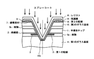
次に、図5に示すように、第2の配線8上に保護膜9を形成する。保護膜9は後のスクリーン印刷工程で、ソルダーマスクとして機能する。この保護膜9は、不図示のスプレーコーターによって、例えばエポキシ樹脂のような有機系樹脂を、同図の矢印方向に、すなわち第2の配線8が形成された面に向けてスプレーコートして、第2の配線8の表面に形成する。
Next, as shown in FIG. 5, a
ここで、上記スプレーコーターは、例えば液状の有機系樹脂に圧力を加えて、これを細いノズルから第2の配線8の形成された面に噴出させることにより、有機系樹脂を霧状の微粒子にする構成を有している。スプレーコーターは係る構成を備えていれば、手動制御でも自動制御でもよい。
Here, the spray coater applies pressure to, for example, a liquid organic resin, and ejects the pressure from a thin nozzle onto the surface on which the
このスプレーコートによれば、保護膜9は、V字型の溝VGを含めて均一な厚さに形成され、V字型の溝VGに厚く溜まることが無くなるため、有機系樹脂の使用量を極力少量に抑えることが可能となる。
According to this spray coating, the
有機系樹脂が熱硬化性樹脂である場合には、保護膜9をスプレーコートした後、所定の温度に加熱してベーキングを行い、保護膜9を熱硬化させる。このとき、保護膜9は、V字型の溝VGに厚く溜まることが無く、均一な厚さに形成されているので、従来のような半導体ウエハ1aの反りは生じない。尚、当該保護膜9はレジスト材料で形成してもよい。
When the organic resin is a thermosetting resin, after the
次に、第2のガラス基板6上方の当該保護膜9の所定位置に、後述する導電端子10を形成するために、第2の配線8が露出するように開口部Kを形成する。この開口部Kは、緩衝部材7がある場合、緩衝部材7と対応する位置に形成する。開口部Kは、以下に示すように、レジスト層Rを用いて形成される。
Next, in order to form a
図6に示すように、例えば液状のレジスト材料を、同図の矢印方向に、すなわち保護膜9が形成された面に向けてスプレーコートして、レジスト層Rを保護膜9の表面に形成する。スプレーコートによるレジスト層Rの形成は、不図示のスプレーコーターによって行われる。
As shown in FIG. 6, for example, a liquid resist material is spray-coated in the direction of the arrow in FIG. 6, that is, toward the surface on which the
ここで、上記スプレーコーターは、例えば液状のレジスト材料に圧力を加えて、これを細いノズルから保護膜9上に噴出させることにより、レジスト材料を霧状の微粒子にする構成を有している。スプレーコーターは係る構成を備えていれば、手動制御でも自動制御でもよい。
Here, the spray coater has a configuration in which, for example, a pressure is applied to a liquid resist material and the resist material is sprayed onto the
このスプレーコートによれば、レジスト層Rは、V字型の溝VGを含めて均一な厚さに形成され、V字型の溝VGに厚く溜まることが無くなるため、レジスト材料の使用量を極力少量に抑えることが可能となる。 According to this spray coating, the resist layer R is formed to have a uniform thickness including the V-shaped groove VG and does not accumulate thickly in the V-shaped groove VG. It becomes possible to suppress to a small amount.
また、レジスト材料が熱硬化性樹脂である場合には、レジスト層Rをスプレーコートした後、所定の温度に加熱してベーキングを行い、レジスト層Rを熱硬化させる。このとき、レジスト層Rは、V字型の溝VGに厚く溜まることが無く、均一な厚さに形成されているので、従来のような半導体ウエハ1aの反りは生じない。 When the resist material is a thermosetting resin, the resist layer R is spray-coated and then heated to a predetermined temperature and baked to thermally cure the resist layer R. At this time, since the resist layer R does not accumulate thickly in the V-shaped groove VG and is formed to have a uniform thickness, the warp of the semiconductor wafer 1a as in the related art does not occur.
次に、図7に示すように、レジスト層Rのうち、緩衝部材7に対応した部分を、例えば不図示のマスクを用いて露光及び現像することにより除去する。そして、図8に示すように、上記部分を除去したレジスト層Rをマスクとして、第2の配線8を露出させるように保護膜9の一部をエッチング等により除去し、開口部Kを形成する。その後、図9に示すようにレジスト層R全体を除去する。
Next, as shown in FIG. 7, a portion of the resist layer R corresponding to the
次に、図10(A)に示すように、開口部Kを有した保護膜9をマスクとして、スクリーン印刷法により、当該開口部Kに露出された第2の配線8上に、半田等の金属から成る導電端子10を形成する。緩衝部材7がある場合、当該導電端子10は、緩衝部材7に対応した位置に配置される。
Next, as shown in FIG. 10A, solder or the like is formed on the
このとき、従来に比べ半導体ウエハ1aの反りの発生が抑制されているので、スクリーン印刷は高精度に行うことができる。即ち、スクリーン印刷のように、半導体ウエハの平坦性が問題となる工程の精度を向上させることができ、BGA型の半導体装置の歩留まりや信頼性を向上できる。そして、その後のリフロー工程を行う。これにより、当該導電端子10はボール状の形状になる。次に、図10(B)に示すように、境界ラインSに沿ってダイシングを行い、個々の半導体チップ1に分割する。これより、BGA型の半導体装置が完成する。
At this time, since the occurrence of warpage of the semiconductor wafer 1a is suppressed as compared with the conventional case, screen printing can be performed with high accuracy. That is, as in screen printing, the accuracy of a process in which flatness of a semiconductor wafer is a problem can be improved, and the yield and reliability of a BGA type semiconductor device can be improved. Then, the subsequent reflow process is performed. Thus, the
なお、上記実施形態では、開口部Kを形成するためのレジスト層Rを、スプレーコートにより保護膜9上に形成したが、本発明は、これに限定されない。即ち、パターニング時のマスク材としてレジスト層を使用する諸工程において、スプレーコートを用いて当該レジスト層を形成してもよい。
In the above embodiment, the resist layer R for forming the opening K is formed on the
また、上記実施形態では、信頼性を確保するために半導体ウエハ1aに第1のガラス基板4、第2のガラス基板6を貼り合わせているが、工程を簡略化するためには、第2のガラス基板6を省略してもよい。この場合、図2の工程におけるバックグラインドの後、半導体ウエハ1aをその裏面側から境界ラインSに沿ってエッチングして溝を形成し、第1の配線3を露出させる。このエッチングは、レジスト層を形成して行うが、このレジスト層は、スプレーコートにより、レジスト材料を半導体ウェハ1aの裏面に塗布して形成される。
Moreover, in the said embodiment, in order to ensure reliability, the 1st glass substrate 4 and the 2nd glass substrate 6 are bonded together to the semiconductor wafer 1a, but in order to simplify a process, it is 2nd. The glass substrate 6 may be omitted. In this case, after the back grinding in the process of FIG. 2, the semiconductor wafer 1 a is etched from the back surface side along the boundary line S to form a groove, and the
そして、チップ裏面側に緩衝部材7を形成する場合は、スプレーコートにより、半導体ウェハ1aの裏面に緩衝部材7を形成する。さらに、第2の配線8を、半導体ウェハ1a(半導体チップ1)の裏面に形成して、その後、スプレーコートにより、第2の配線8上に保護膜9を形成する。
When the
さらにまた、上記実施形態では、本発明を、半導体チップの裏面に導電端子を有するBGA型の半導体装置に適用しているが、本発明はこれに限らず、半導体チップの裏面に導電端子を有さない、いわゆるLGA(Land Grid Array)型の半導体装置に本発明を適用しても良い。即ち、第2の配線8の表面に保護膜9を形成し、この保護膜9の開口部Kに導電端子10を形成しない状態の半導体装置を構成するものである。
Furthermore, in the above embodiment, the present invention is applied to a BGA type semiconductor device having a conductive terminal on the back surface of the semiconductor chip. However, the present invention is not limited to this, and the conductive terminal is provided on the back surface of the semiconductor chip. However, the present invention may be applied to a so-called LGA (Land Grid Array) type semiconductor device. That is, a semiconductor device is formed in which the
Claims (15)
前記半導体ウエハの裏面側に第2の支持基板を貼り合わせる工程と、
前記第2の支持基板の裏面からダイシングラインに沿って、前記第1の支持基板に至るまで切削を行うことによって溝を形成し、前記第1の配線を部分的に露出させる工程と、
前記溝内で、前記第1の配線の露出部分に接続され、前記第2の支持基板の裏面に延在する第2の配線を形成する工程と、
スプレーコートにより、前記溝内を完全に埋め込むことなく、前記溝内から前記第2の支持基板上に延在する前記第2の配線上に有機系樹脂から成る保護膜を形成する工程と、
前記保護膜の所定位置に前記第2の配線を露出する開口部を形成する工程と、を具備することを特徴とする半導体装置の製造方法。 Bonding the first support substrate to the surface side of the semiconductor wafer on which the first wiring is formed;
Bonding a second support substrate to the back side of the semiconductor wafer;
Forming a groove by cutting from the back surface of the second support substrate along the dicing line to the first support substrate, and partially exposing the first wiring;
Forming a second wiring connected to an exposed portion of the first wiring in the groove and extending to the back surface of the second support substrate;
Forming a protective film made of an organic resin on the second wiring extending from the groove to the second support substrate without completely filling the groove by spray coating;
And a step of forming an opening exposing the second wiring at a predetermined position of the protective film.
前記半導体ウエハの裏面に溝を形成し、前記第1の配線を部分的に露出させる工程と、
前記溝内で、前記第1の配線の露出部分に接続され、前記半導体ウエハの裏面に延在する第2の配線を形成する工程と、
スプレーコートにより、前記溝内を完全に埋め込むことなく、前記溝内から前記半導体ウエハ上に延在する前記第2の配線上に有機系樹脂から成る保護膜を形成する工程と、
前記保護膜の所定位置に前記第2の配線を露出する開口部を形成する工程と、を具備することを特徴とする半導体装置の製造方法。 Bonding a support substrate on the surface of the semiconductor wafer on which the first wiring is formed;
Forming a groove on a back surface of the semiconductor wafer to partially expose the first wiring;
Forming a second wiring connected to an exposed portion of the first wiring and extending to a back surface of the semiconductor wafer in the groove;
Forming a protective film made of an organic resin on the second wiring extending from the groove to the semiconductor wafer without completely filling the groove by spray coating;
And a step of forming an opening exposing the second wiring at a predetermined position of the protective film.
前記半導体ウエハを、当該半導体ウエハの裏面からダイシングラインに沿ってエッチングして、複数の半導体チップに分離する工程と、
前記複数の半導体チップの裏面側に、樹脂を介して第2の支持基板を貼り合わせる工程と、
前記ダイシングラインに沿って、前記第2の支持基板の裏面から、前記第2の支持基板及び前記樹脂を切削し、さらに前記第1の支持基板の一部を切削することによって溝を形成し、前記第1の配線を部分的に露出させる工程と、
前記溝内で、前記第1の配線の露出部分に接続され、前記第2の支持基板の裏面に延在する第2の配線を形成する工程と、
スプレーコートにより、前記溝内を完全に埋め込むことなく、前記溝内から前記第2の支持基板上に延在する前記第2の配線上に有機系樹脂から成る保護膜を形成する工程と、
前記保護膜の所定位置に前記第2の配線を露出する開口部を形成する工程と、を具備することを特徴とする半導体装置の製造方法。 Bonding the first support substrate on the surface of the semiconductor wafer on which the first wiring is formed;
Etching the semiconductor wafer along a dicing line from the back surface of the semiconductor wafer, and separating the semiconductor wafer into a plurality of semiconductor chips;
Bonding the second support substrate to the back side of the plurality of semiconductor chips via a resin;
Along the dicing line, from the back surface of the second support substrate, cut the second support substrate and the resin, and further form a groove by cutting a part of the first support substrate, Partially exposing the first wiring;
Forming a second wiring connected to an exposed portion of the first wiring in the groove and extending to the back surface of the second support substrate;
Forming a protective film made of an organic resin on the second wiring extending from the groove to the second support substrate without completely filling the groove by spray coating;
And a step of forming an opening exposing the second wiring at a predetermined position of the protective film.
Priority Applications (1)
| Application Number | Priority Date | Filing Date | Title |
|---|---|---|---|
| JP2003356195A JP4562371B2 (en) | 2002-10-30 | 2003-10-16 | Manufacturing method of semiconductor device |
Applications Claiming Priority (2)
| Application Number | Priority Date | Filing Date | Title |
|---|---|---|---|
| JP2002315418 | 2002-10-30 | ||
| JP2003356195A JP4562371B2 (en) | 2002-10-30 | 2003-10-16 | Manufacturing method of semiconductor device |
Related Child Applications (1)
| Application Number | Title | Priority Date | Filing Date |
|---|---|---|---|
| JP2010021808A Division JP5258807B2 (en) | 2002-10-30 | 2010-02-03 | Manufacturing method of semiconductor device |
Publications (3)
| Publication Number | Publication Date |
|---|---|
| JP2004172587A JP2004172587A (en) | 2004-06-17 |
| JP2004172587A5 JP2004172587A5 (en) | 2006-11-30 |
| JP4562371B2 true JP4562371B2 (en) | 2010-10-13 |
Family
ID=32715788
Family Applications (1)
| Application Number | Title | Priority Date | Filing Date |
|---|---|---|---|
| JP2003356195A Expired - Fee Related JP4562371B2 (en) | 2002-10-30 | 2003-10-16 | Manufacturing method of semiconductor device |
Country Status (1)
| Country | Link |
|---|---|
| JP (1) | JP4562371B2 (en) |
Families Citing this family (3)
| Publication number | Priority date | Publication date | Assignee | Title |
|---|---|---|---|---|
| JP4936695B2 (en) * | 2004-09-29 | 2012-05-23 | オンセミコンダクター・トレーディング・リミテッド | Semiconductor device and manufacturing method thereof |
| JP2008166381A (en) * | 2006-12-27 | 2008-07-17 | Sanyo Electric Co Ltd | Semiconductor device and manufacturing method therefor |
| JP5101157B2 (en) * | 2007-05-07 | 2012-12-19 | オンセミコンダクター・トレーディング・リミテッド | Manufacturing method of semiconductor device |
Citations (5)
| Publication number | Priority date | Publication date | Assignee | Title |
|---|---|---|---|---|
| JP2001053033A (en) * | 1999-08-12 | 2001-02-23 | Texas Instr Japan Ltd | Dicing method of semiconductor device |
| JP2001326299A (en) * | 2000-05-18 | 2001-11-22 | Iep Technologies:Kk | Semiconductor device and method for manufacturing the same |
| JP2001332643A (en) * | 2000-05-19 | 2001-11-30 | Iep Technologies:Kk | Semiconductor device and its manufacturing method |
| JP2002512436A (en) * | 1998-02-06 | 2002-04-23 | シェルケース リミティド | Integrated circuit device |
| JP2002208655A (en) * | 2000-06-02 | 2002-07-26 | Seiko Epson Corp | Semiconductor device and its manufacturing method, laminated semiconductor device, circuit board and electronic equipment |
-
2003
- 2003-10-16 JP JP2003356195A patent/JP4562371B2/en not_active Expired - Fee Related
Patent Citations (5)
| Publication number | Priority date | Publication date | Assignee | Title |
|---|---|---|---|---|
| JP2002512436A (en) * | 1998-02-06 | 2002-04-23 | シェルケース リミティド | Integrated circuit device |
| JP2001053033A (en) * | 1999-08-12 | 2001-02-23 | Texas Instr Japan Ltd | Dicing method of semiconductor device |
| JP2001326299A (en) * | 2000-05-18 | 2001-11-22 | Iep Technologies:Kk | Semiconductor device and method for manufacturing the same |
| JP2001332643A (en) * | 2000-05-19 | 2001-11-30 | Iep Technologies:Kk | Semiconductor device and its manufacturing method |
| JP2002208655A (en) * | 2000-06-02 | 2002-07-26 | Seiko Epson Corp | Semiconductor device and its manufacturing method, laminated semiconductor device, circuit board and electronic equipment |
Also Published As
| Publication number | Publication date |
|---|---|
| JP2004172587A (en) | 2004-06-17 |
Similar Documents
| Publication | Publication Date | Title |
|---|---|---|
| JP5258807B2 (en) | Manufacturing method of semiconductor device | |
| KR100510556B1 (en) | Semiconductor package having ultra thin thickness and method for manufacturing the same | |
| JP3842548B2 (en) | Semiconductor device manufacturing method and semiconductor device | |
| JP2008244437A (en) | Image sensor package having die receiving opening and method thereof | |
| US6849955B2 (en) | High density integrated circuit packages and method for the same | |
| KR20060101385A (en) | A semiconductor device and a manufacturing method of the same | |
| JP2003197856A (en) | Semiconductor device | |
| US20080197480A1 (en) | Semiconductor device package with multi-chips and method of the same | |
| JP2009094434A (en) | Semiconductor device, and manufacturing method of the same | |
| US6489667B1 (en) | Semiconductor device and method of manufacturing such device | |
| JPH053183A (en) | Semiconductor device and manufacture thereof | |
| JPH11354560A (en) | Manufacture of semiconductor device | |
| JP4963989B2 (en) | Semiconductor device mounting substrate and manufacturing method thereof | |
| JP2006351950A (en) | Semiconductor device and method for manufacturing the same | |
| US6919264B2 (en) | Method for the solder-stop structuring of elevations on wafers | |
| JP5238985B2 (en) | Manufacturing method of semiconductor device | |
| JP4562371B2 (en) | Manufacturing method of semiconductor device | |
| JP2002313985A (en) | Method of manufacturing chip size package | |
| JP2010016395A5 (en) | ||
| JP3877700B2 (en) | Semiconductor device and manufacturing method thereof | |
| JP3522403B2 (en) | Semiconductor device | |
| JP4401330B2 (en) | Semiconductor device and manufacturing method thereof | |
| JP4522213B2 (en) | Manufacturing method of semiconductor device | |
| JP4805362B2 (en) | Manufacturing method of semiconductor device | |
| JP3381833B2 (en) | BGA type semiconductor device and manufacturing method thereof |
Legal Events
| Date | Code | Title | Description |
|---|---|---|---|
| A521 | Written amendment |
Free format text: JAPANESE INTERMEDIATE CODE: A523 Effective date: 20061016 |
|
| A621 | Written request for application examination |
Free format text: JAPANESE INTERMEDIATE CODE: A621 Effective date: 20061016 |
|
| A977 | Report on retrieval |
Free format text: JAPANESE INTERMEDIATE CODE: A971007 Effective date: 20070205 |
|
| A131 | Notification of reasons for refusal |
Free format text: JAPANESE INTERMEDIATE CODE: A131 Effective date: 20090805 |
|
| A521 | Written amendment |
Free format text: JAPANESE INTERMEDIATE CODE: A523 Effective date: 20091002 |
|
| A131 | Notification of reasons for refusal |
Free format text: JAPANESE INTERMEDIATE CODE: A131 Effective date: 20091217 |
|
| A521 | Written amendment |
Free format text: JAPANESE INTERMEDIATE CODE: A523 Effective date: 20100203 |
|
| A131 | Notification of reasons for refusal |
Free format text: JAPANESE INTERMEDIATE CODE: A131 Effective date: 20100426 |
|
| A521 | Written amendment |
Free format text: JAPANESE INTERMEDIATE CODE: A523 Effective date: 20100521 |
|
| TRDD | Decision of grant or rejection written | ||
| A01 | Written decision to grant a patent or to grant a registration (utility model) |
Free format text: JAPANESE INTERMEDIATE CODE: A01 Effective date: 20100701 |
|
| A01 | Written decision to grant a patent or to grant a registration (utility model) |
Free format text: JAPANESE INTERMEDIATE CODE: A01 |
|
| A61 | First payment of annual fees (during grant procedure) |
Free format text: JAPANESE INTERMEDIATE CODE: A61 Effective date: 20100727 |
|
| FPAY | Renewal fee payment (event date is renewal date of database) |
Free format text: PAYMENT UNTIL: 20130806 Year of fee payment: 3 |
|
| FPAY | Renewal fee payment (event date is renewal date of database) |
Free format text: PAYMENT UNTIL: 20130806 Year of fee payment: 3 |
|
| R250 | Receipt of annual fees |
Free format text: JAPANESE INTERMEDIATE CODE: R250 |
|
| LAPS | Cancellation because of no payment of annual fees |