JP4550185B2 - Method for manufacturing DRAM device - Google Patents
Method for manufacturing DRAM device Download PDFInfo
- Publication number
- JP4550185B2 JP4550185B2 JP19778599A JP19778599A JP4550185B2 JP 4550185 B2 JP4550185 B2 JP 4550185B2 JP 19778599 A JP19778599 A JP 19778599A JP 19778599 A JP19778599 A JP 19778599A JP 4550185 B2 JP4550185 B2 JP 4550185B2
- Authority
- JP
- Japan
- Prior art keywords
- insulating film
- storage node
- storage
- film
- contact plug
- Prior art date
- Legal status (The legal status is an assumption and is not a legal conclusion. Google has not performed a legal analysis and makes no representation as to the accuracy of the status listed.)
- Expired - Fee Related
Links
- 238000000034 method Methods 0.000 title claims description 52
- 238000004519 manufacturing process Methods 0.000 title claims description 32
- 238000003860 storage Methods 0.000 claims description 122
- 239000010410 layer Substances 0.000 claims description 40
- 238000005530 etching Methods 0.000 claims description 39
- 239000000463 material Substances 0.000 claims description 30
- 239000000758 substrate Substances 0.000 claims description 20
- 239000004065 semiconductor Substances 0.000 claims description 19
- 229910021420 polycrystalline silicon Inorganic materials 0.000 claims description 18
- 229920005591 polysilicon Polymers 0.000 claims description 18
- 230000015572 biosynthetic process Effects 0.000 claims description 9
- 239000005380 borophosphosilicate glass Substances 0.000 claims description 6
- 238000010438 heat treatment Methods 0.000 claims description 6
- 229910052814 silicon oxide Inorganic materials 0.000 claims description 5
- 239000002344 surface layer Substances 0.000 claims description 4
- 238000002425 crystallisation Methods 0.000 claims description 3
- 230000008025 crystallization Effects 0.000 claims description 3
- 230000000149 penetrating effect Effects 0.000 claims description 3
- VYPSYNLAJGMNEJ-UHFFFAOYSA-N Silicium dioxide Chemical compound O=[Si]=O VYPSYNLAJGMNEJ-UHFFFAOYSA-N 0.000 claims 1
- 229920002120 photoresistant polymer Polymers 0.000 description 22
- 239000003990 capacitor Substances 0.000 description 11
- 125000006850 spacer group Chemical group 0.000 description 10
- 229910052581 Si3N4 Inorganic materials 0.000 description 8
- 238000010586 diagram Methods 0.000 description 7
- HQVNEWCFYHHQES-UHFFFAOYSA-N silicon nitride Chemical compound N12[Si]34N5[Si]62N3[Si]51N64 HQVNEWCFYHHQES-UHFFFAOYSA-N 0.000 description 7
- 230000004888 barrier function Effects 0.000 description 6
- 238000002955 isolation Methods 0.000 description 5
- 238000000206 photolithography Methods 0.000 description 5
- 239000011229 interlayer Substances 0.000 description 4
- 238000007796 conventional method Methods 0.000 description 3
- 238000009792 diffusion process Methods 0.000 description 2
- 230000000694 effects Effects 0.000 description 2
- 230000010354 integration Effects 0.000 description 2
- 239000011538 cleaning material Substances 0.000 description 1
- 238000001312 dry etching Methods 0.000 description 1
- 239000011521 glass Substances 0.000 description 1
- 239000012535 impurity Substances 0.000 description 1
- 150000002500 ions Chemical class 0.000 description 1
- 150000004767 nitrides Chemical class 0.000 description 1
- 230000035515 penetration Effects 0.000 description 1
- 230000002093 peripheral effect Effects 0.000 description 1
- 239000012466 permeate Substances 0.000 description 1
- 238000001259 photo etching Methods 0.000 description 1
- 238000005498 polishing Methods 0.000 description 1
- 239000000126 substance Substances 0.000 description 1
- 238000001039 wet etching Methods 0.000 description 1
Images


Classifications
-
- H—ELECTRICITY
- H01—ELECTRIC ELEMENTS
- H01L—SEMICONDUCTOR DEVICES NOT COVERED BY CLASS H10
- H01L27/00—Devices consisting of a plurality of semiconductor or other solid-state components formed in or on a common substrate
- H01L27/02—Devices consisting of a plurality of semiconductor or other solid-state components formed in or on a common substrate including semiconductor components specially adapted for rectifying, oscillating, amplifying or switching and having potential barriers; including integrated passive circuit elements having potential barriers
- H01L27/04—Devices consisting of a plurality of semiconductor or other solid-state components formed in or on a common substrate including semiconductor components specially adapted for rectifying, oscillating, amplifying or switching and having potential barriers; including integrated passive circuit elements having potential barriers the substrate being a semiconductor body
- H01L27/10—Devices consisting of a plurality of semiconductor or other solid-state components formed in or on a common substrate including semiconductor components specially adapted for rectifying, oscillating, amplifying or switching and having potential barriers; including integrated passive circuit elements having potential barriers the substrate being a semiconductor body including a plurality of individual components in a repetitive configuration
-
- H—ELECTRICITY
- H01—ELECTRIC ELEMENTS
- H01L—SEMICONDUCTOR DEVICES NOT COVERED BY CLASS H10
- H01L28/00—Passive two-terminal components without a potential-jump or surface barrier for integrated circuits; Details thereof; Multistep manufacturing processes therefor
- H01L28/40—Capacitors
- H01L28/60—Electrodes
-
- H—ELECTRICITY
- H01—ELECTRIC ELEMENTS
- H01L—SEMICONDUCTOR DEVICES NOT COVERED BY CLASS H10
- H01L21/00—Processes or apparatus adapted for the manufacture or treatment of semiconductor or solid state devices or of parts thereof
- H01L21/70—Manufacture or treatment of devices consisting of a plurality of solid state components formed in or on a common substrate or of parts thereof; Manufacture of integrated circuit devices or of parts thereof
- H01L21/71—Manufacture of specific parts of devices defined in group H01L21/70
- H01L21/768—Applying interconnections to be used for carrying current between separate components within a device comprising conductors and dielectrics
- H01L21/76838—Applying interconnections to be used for carrying current between separate components within a device comprising conductors and dielectrics characterised by the formation and the after-treatment of the conductors
- H01L21/76895—Local interconnects; Local pads, as exemplified by patent document EP0896365
-
- H—ELECTRICITY
- H01—ELECTRIC ELEMENTS
- H01L—SEMICONDUCTOR DEVICES NOT COVERED BY CLASS H10
- H01L28/00—Passive two-terminal components without a potential-jump or surface barrier for integrated circuits; Details thereof; Multistep manufacturing processes therefor
- H01L28/40—Capacitors
- H01L28/60—Electrodes
- H01L28/82—Electrodes with an enlarged surface, e.g. formed by texturisation
- H01L28/84—Electrodes with an enlarged surface, e.g. formed by texturisation being a rough surface, e.g. using hemispherical grains
Landscapes
- Engineering & Computer Science (AREA)
- Power Engineering (AREA)
- Computer Hardware Design (AREA)
- Microelectronics & Electronic Packaging (AREA)
- Physics & Mathematics (AREA)
- Condensed Matter Physics & Semiconductors (AREA)
- General Physics & Mathematics (AREA)
- Manufacturing & Machinery (AREA)
- Semiconductor Memories (AREA)
- Internal Circuitry In Semiconductor Integrated Circuit Devices (AREA)
Description
【0001】
【発明の属する技術分野】
本発明は、半導体装置の製造方法に関するものであり、より詳しくは、DRAMの製造方法に関するものである。
【0002】
【従来の技術】
DRAM装置は、スタック型(stack)とトレンチ型(trench)に区分され、DRAM装置が高集積化されることによって、トレンチ型よりは、スタック型のキャパシタが主にDRAM装置に適用されることに期待される。従って、以後本発明を、スタック型のキャパシタに観点をおいて述べる。
【0003】
DRAM装置が高集積化されることによって、DRAM装置を構成する素子は、スケールダウン(scaling down)されている。DRAM装置の高集積化によってそれを構成する素子のスケールダウンは、キャパシタのキャパシタンスを維持させることにおいて、多くの難しさを発生させるだけではなく、素子を形成するために行われるフォト及びエッチング工程でも多くの難点と問題を発生させている。
【0004】
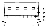
図1乃至図2は、誤整列のとき、従来DRAM装置の製造工程を順序に示す図面である。
まず、図1及び図2を参照すると、半導体基板10上にビットライン16を含んで形成された層間絶縁膜14を貫通して素子隔離領域、即ちSTI(shallow trench isolation)12の間の半導体基板10と電気的に連結される障壁コンタクト(buried contact)、即ちストレージコンタクトプラグ18が形成される。続いて層間絶縁膜14上にストレージノード形成のためのポリシリコン膜20が形成される。
【0005】
図3を参照すると、フォトリソグラフィ工程でポリシリコン膜上にストレージノード形成領域を定義するためのマスク(未図示)が形成された後、マスクを使用するポリシリコン膜工程でストレージノード20aが形成される。そして、ストレージノードの有効表面積を増加させるために、ストレージノード表面上にHSG(hemisphrical glass)(未図示)膜が形成される。続いて、ストレージノードを含んで絶縁膜上にキャパシタ形成用誘電膜(未図示)が蒸着され、上部電極用導電膜(未図示)が形成されてセルキャパシタが形成される。
【0006】
しかし、このようなDRAM装置のキャパシタ形成方法では、マスクがストレージコンタクトプラグ18に誤整列された場合、次のような問題がある。通常、ポリシリコン膜20のエッチング工程は、ストレージノード20aの間の電気的ブリッジ(bridge)を防止するためにポリシリコンの過エッチング工程を含む。この過エッチング工程で誤整列されたストレージコンタクトプラグ18の上部領域のポリシリコン膜が過エッチングされ、又後続洗浄物質によってストレージノードと接する層間絶縁膜14が過エッチングされて、ストレージノード20aがストレージコンタクトプラグ18及び層間絶縁膜14と接する面積が非常に小さくなる。
【0007】
ストレージノード20aとストレージコンタクトプラグ18との接触面の減少は、抵抗の増加を招き、又後続工程でストレージノード20aが倒れたり、折れたりする問題が生じる。このような問題は、DRAM装置が高集積度化されることによって、より深刻になり、1G DRAM級以上高集積装置では避けられない問題になる。
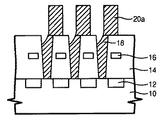
【0008】
従って、このような問題を解決するために提案された方法のうち、1つがストレージノードをリバース型で形成する方法である。即ち、ダマシン工程(damascene process)を応用してストレージノードを形成する方法である。
まず、半導体基板50上に形成されたビットライン56を含む第1絶縁膜54を貫いてSTI52の間の半導体基板50と電気的に連結されるストレージコンタクトプラグ60が形成される。
【0009】
続いて、第1絶縁膜54上に第2絶縁膜62が形成される。第2絶縁膜62が部分的にエッチングされて、ストレージコンタクトプラグ60の上部表面が露出されるストレージノード形成領域であるオープニングが形成される。続いて、オープニングがポリシリコンで充填されてストレージノード64が形成された後、ストレージノード64両側の第2絶縁膜62がエッチングされて露出されるストレージノードの表面積を制御することによって必要とするキャパシタのキャパシタンスを確保するようになる。
【0010】
しかし、この方法は、ストレージノード両側の第2絶縁膜62エッチング工程で通常的に利用される湿式や乾式エッチング工程でエッチングされる第2絶縁膜62の量によってキャパシタのキャパシタンスが変わる問題があるし、又第2絶縁膜62が過度にエッチングされると、DRAM装置の周辺回路領域にビットラインが露出されて後続上部電極形成のとき、ビットラインが損傷される問題が生じる。
【0011】
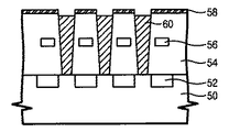
図4乃至図6は、誤整列のとき、他の従来のDRAM装置の製造工程を順序に示す図面である。
図4を参照すると、前述の問題を解決するためにシリコン窒化膜のような酸化膜に対するエッチング選択比が高いエッチング停止膜がストレージコンタクトプラグ60の形成前や後に第1絶縁膜54上に形成されることが普通である。
【0012】
図5及び図6を参照すると、ストレージノード形成領域とストレージコンタクトプラグ60が誤整列された場合、ストレージノードが形成された後、第2絶縁膜62のエッチング工程のうち、ストレージコンタクトプラグの上部領域にある第1絶縁膜54の一部がエッチングされたり、又は第2絶縁膜58工程で使用されるエッチング物質がストレージノード64とシリコン窒化膜との界面に沿って浸透して第1絶縁膜をエッチングして、図6に図示されたようなリセス領域を発生するようになる。これにより、キャパシタの誘電膜漏洩(dielectric leakage)が発生し、上部電極のステップカバレージ(step coverage)不良等のようにDRAM装置の信頼性に多くの問題が発生される。
【0013】
【発明が解決しようとする課題】
本発明は、上述の問題点を解決するために提案されたものとして、ストレージノードがストレージコンタクトプラグに誤整列されてもストレージコンタクトプラグを含む絶縁膜とストレージコンタクトプラグを形成するポリシリコンの過エッチングを防止することができ、又ストレージノードとストレージコンタクトプラグとの間の接触面積を増加させることができるため、より向上された性能を発揮することができるDRAM装置の製造方法を提供することである。
【0014】
【課題を解決するための手段】
上述の目的を達成するために提案された本発明の特徴によると、DRAM装置の製造方法は、半導体基板上に形成された第1絶縁膜を通過して半導体基板と電気的に接続されるようにストレージコンタクトプラグを形成する段階と、ストレージコンタクトプラグを含んで第1絶縁膜上に第2絶縁膜、物質層、そして第3絶縁膜を順序形成する段階と、物質層は、第3絶縁膜のエッチング物質が第2絶縁膜を浸透することを防止し、ストレージノード形成用マスクを使用して第3絶縁膜、物質層、そして第2絶縁膜を順序エッチングしてストレージコンタクトプラグ及び第1絶縁膜一部の上部表面を露出させるオープニングを形成する段階と、オープニングを導電膜で充填してストレージノードを形成する段階と、ストレージノード両側の物質層の上部表面が露出されるときまで、第3絶縁膜をエッチングする段階と、ストレージノード両側の第2絶縁膜の上部表面が露出されるときまで、物質層をエッチングする段階とを含む。
【0015】
上述の目的を達成するために提案された本発明の特徴によると、ゲートが形成された半導体基板上に第1絶縁膜を形成する段階と、第1絶縁膜上に上部表面が第1絶縁膜と他のエッチング選択比を有する第2絶縁膜で覆われたビットラインを形成する段階と、第2絶縁膜及びビットラインの両側壁に第1絶縁膜と他の選択比を有するスペーサを形成する段階と、ビットラインを含んで第1絶縁膜上に第2絶縁膜及びスペーサと相異なるエッチング選択比を有する第3絶縁膜を形成する段階と、ストレージコンタクト領域を定義するためのマスクを使用して第3絶縁膜と第1絶縁膜をエッチングしてビットラインとビットラインとの間を通過する自己整列型ストレージコンタクトホールを形成する段階と、ストレージコンタクトホールを導電膜で充填してストレージコンタクトプラグを形成する段階とを含む。
【0016】
【発明の実施の形態】
図10及び図11を参照すると、本発明の実施形態による新たなDRAM装置の製造方法は、ストレージコンタクトプラグを含んで第1絶縁膜上に第2絶縁膜、第3絶縁膜のエッチング物質が第2絶縁膜に浸透することを防止する物質層、そして第3絶縁膜が順次形成され、ストレージノード形成用マスクを使用して第3絶縁膜、物質層、そして第2絶縁膜が順次エッチングされてオープニングが形成され、オープニングが導電膜であるポリシリコン膜で充填されてストレージノードが形成される。
【0017】
このようなDRAM装置の製造方法によって、ストレージノードの下部領域でストレージノードを形成するポリシリコンの過エッチングを防止することができ、領域で絶縁膜の過エッチングで発生される誘電膜漏洩及び上部電極のステップカバレージ不良等の問題を防止することができる。又、第1絶縁膜上に上部表面が第1絶縁膜と他のエッチング比を有する第2絶縁膜で覆われたビットラインが形成され、第2絶縁膜及びビットラインの両側壁に第1絶縁膜と他のエッチング選択比を有するスペーサが形成される。
【0018】
ビットラインを含んで第1絶縁膜上に第3絶縁膜が形成され、ストレージコンタクト領域を定義するためのマスクを使用して第3絶縁膜と第1絶縁膜をエッチングしてビットラインとビットラインとを通過する自己整列型ストレージコンタクトホールが形成される。このようなDRAM装置の製造方法によって、導電膜でストレージコンタクトホールが充填されて形成されるストレージコンタクトプラグ、即ち障壁コンタクトの上部直径を広げることができるため、ストレージノードとのオーバーラップマージンを十分に確保することができ、ストレージノードと障壁コンタクトの接触面積を従来の製造方法でより大きく確保することができるため、素子の接触抵抗も減少させることができる。
【0019】
(第1実施形態)
以下、図7乃至図10を参照して、本発明の第1実施例を詳細に説明する。
図7乃至図10は、本発明によるDRAMセルキャパシタの製造方法を順序に示す流れ図である。
図7を参照すると、本発明の第1実施形態によるDRAMセルキャパシタの製造方法では、まず半導体基板100上に活性領域と非活性領域を定義して素子隔離領域102が形成され、活性領域上にセルトランジスター(未図示)が形成される。
【0020】
セルトランジスターは、半導体基板上にゲート酸化膜を間に置いて形成されたゲート電極とゲート電極の両側にある半導体基板内に形成されたソース/ドレーン拡散層を含む。続いてセルトランジスターのゲート電極の間にはソース/ドレーン拡散層と電気的に連結されるパッドが形成される。セルトランジスターを含んで半導体基板上にビットライン106を含んで第1絶縁膜104が形成される。例えば、第1絶縁膜104は、USG、BPSG、HDP、そしてO3−TEOSのうち、いずれか1つで形成されることができる。
【0021】
第1絶縁膜104上にフォトレジスト膜(未図示)が形成され、公知のフォトリソグラフィ工程によって、フォトレジスト膜がパターニングされてストレージコンタクトホール形成領域を定義する第1フォトレジストパターンが形成される。
【0022】
第1フォトレジストパターンがマスクとして使用されて第1絶縁膜104が部分的にエッチングされてパッドの上部表面を露出させるストレージコンタクトホールが形成され、続いて第1フォトレジストパターンが除去される。第1絶縁膜上にストレージコンタクトホールが充填されるように第1導電膜が形成された後、ストレージコンタクトホール両側の第1絶縁膜上にある不必要な第1導電膜が除去されてストレージコンタクトプラグ108が形成される。例えば、第1導電膜は、不純物イオンでドーピングされたポリシリコン膜で形成されることができる。第1導電膜のエッチングは、CMP(Chemical Mechanical Polishing)工程やポリシリコンエッチバック(etchback)工程で実施されることができる。
【0023】
続いて、ストレージコンタクトプラグ108の結晶化のための熱処理が行われる。熱処理工程は、約550℃以上の温度で実施されるが、これはストレージコンタクトプラグと後続工程で形成されるストレージノードが誤整列された場合、ストレージノードの有効表面積を増加させるために形成されるHSG膜がストレージコンタクトプラグ上部表面に形成されてストレージノードの間に電気的ブリッジを発生させることを防止するためのものである。これは、結晶化されたポリシリコン膜上にはHSG膜が成長されないためである。ストレージコンタクトプラグ108が形成された後、HSG(HSG)膜形成前に行われる工程のうち、約550℃以上の温度で行われる工程があると、熱処理工程は、排除されることができる。
【0024】
第1絶縁膜104上に第2絶縁膜110が形成される。例えば、第2絶縁膜は、シリコン窒化膜で形成されることができるが、望ましくは、SiNやSiONで形成されることができる。第2絶縁膜は、後続工程で形成されるストレージノードとストレージコンタクトプラグ108が誤整列された場合、後続工程で形成される後続工程で形成される物質層エッチングのとき、ストレージコンタクトプラグの上部領域がエッチングされることを防止する。第2絶縁膜110は、約100〜500Å範囲内の厚さを有するように形成されることができる。
【0025】
第2絶縁膜110上に、後続工程で形成される第4絶縁膜のエッチングのとき、使用されるエッチング物質が第1絶縁膜で浸透することを防ぐすることによって、第1絶縁膜がエッチングされることを防止することができる物質層112が形成される。例えば、物質層112は、約300〜1000Å範囲内の厚さを有するポリシリコン膜で形成されることができる。
【0026】
物質層112上に、第3絶縁膜114が形成される。例えば、第3絶縁膜112は、約6000〜15000Å範囲内の厚さを有するUSG、BPSG、HDP、そしてO3−TEOSのうち、いずれか1つで形成されることができる。第3絶縁膜114上に第2フォトレジスト膜が形成される。公知のフォトリソグラフィ工程によって第2フォトレジスト膜がパターニングされて第2フォトレジストパターンが形成される。第2フォトレジストパターンがマスクとして使用されて第3絶縁膜114、物質層112、そして第2絶縁膜110が順次エッチングされて第1絶縁膜104の一部上部表面とストレージコンタクトプラグ108の上部表面を露出させるオープニングが形成される。第2フォトレジストパターンが除去された後、オープニングが充填されるように第3絶縁膜114上に第2導電膜が形成される。オープニング両側の第3絶縁膜上にある不必要な第2導電膜が除去されてストレージノード116が形成される。
【0027】
次に、ストレージノード116両側の物質層112が露出されるときまで、第3絶縁膜114がエッチングされる。この場合、前述のように、物質層112は、第3窒化膜114のエッチング工程で使用されるエッチング物質が第2絶縁膜110、即ち、シリコン窒化膜とストレージノード側壁との界面に沿って浸透することを防止して第1絶縁膜104である酸化膜系列の絶縁膜がエッチングされることを防止する。又、エッチング工程で物質層112は、エッチング停止層として作用して第3絶縁膜114のエッチング工程が安定的に行われることができるようにする。
【0028】
続いて、第3絶縁膜114がエッチングされた後、物質層112がエッチングされる。ストレージノード116間の電気的ブリッジを防止するためポリシリコンで形成された物質層112は除去されなければならない。この工程から、第2絶縁膜110は、ストレージのノード116とストレージコンタクトプラグ108が誤整列された場合、物質層112エッチング工程のうち、ストレージコンタクトプラグ108がエッチングされることを防止する。
【0029】
物質層112がエッチングされた後、第1絶縁膜104の上部表面が露出されるときまで第2絶縁膜110がエッチングされる。この場合、後続工程でストレージノード116の表面積を増加させるためのHSG膜形成工程がなかったら、第2絶縁膜110のエッチング工程は、排除されることができる。
続いて、ストレージノード116の有効表面積を増加させるためにストレージノード表面上に粗い表面層118が形成される。例えば粗い表面層118は、HSG膜で形成されることができる。これにより、より大きいキャパシタのキャパシタンス、即ちより大きい定電用量が確保されることができる。
【0030】
(第2実施形態)
以下、図11を参照して本発明の第2実施例を詳細に説明する。
図11は、誤整列のとき、他の本発明によるDRAM装置を示す図面である。
図11を参照すると、本発明の第2実施形態によるDRAM装置の製造方法は、まず、半導体基板150上に活性領域と非活性領域を定義して素子隔離領域152が形成され、活性領域の半導体基板にセルトランジスター(未図示)が形成される。続いて、セルトランジスターのゲート電極の間に活性領域の半導体基板と電気的に連結されるパッドが形成される。
【0031】
セルトランジスターを含んで半導体基板150上に第1絶縁膜154が形成される。例えば、第1絶縁膜154は、USG、BPSG、HDP、そしてO3−TEOSのうちいずれか1つで形成されることができる。続いて、第1絶縁膜154上に導電膜と第2絶縁膜が順次形成される。例えば、第2絶縁膜は、シリコン窒化膜、即ちSiN、SiONで形成されることができる。
【0032】
第2絶縁膜156上に第1フォトレジスト膜が形成される。第1フォトレジスト膜が公知のフォトリソグラフィ工程でパターニングされて第1フォトレジストパターンが形成される。第1フォトレジストパターンをマスクとして使用して第2絶縁膜と第1導電膜が順次エッチングされて第2絶縁膜156で上部表面が覆われたビットライン158が形成される。続いて、第1フォトレジストパターンが除去された後、ビットライン158を含んで第1絶縁膜154上にスペーサ形成用絶縁膜が形成される。スペーサ形成用絶縁膜が異方性エッチングされてビットライン158及び第2絶縁膜156の両側壁にスペーサ157を形成する。スペーサ157は、シリコン窒化膜、即ちSiN、SiONで形成されることができる。これにより、ビットライン158は、第1絶縁膜154とエチング選択比が他の第2絶縁膜156とスペーサ157で囲まれている。
【0033】
次に、第1絶縁膜154上にビットラインを含んで第3絶縁膜160が形成される。例えば、第3絶縁膜160は、USG、BPSG、HDP、そしてO3−TEOSのうち、いずれか1つで形成されることができる。
【0034】
第3絶縁膜160上に第2フォトレジスト膜が形成される。第2フォトレジスト膜が公知のフォトリソグラフィ工程によってエッチングされて第2フォトレジストパターンが形成される。第2フォトレジストパターンをマスクとして使用して第3絶縁膜160及び第1絶縁膜154がエッチングされてパッドの一部上部表面が露出される自己整列型ストレージコンタクトホール162が形成される。
この場合、ストレージコンタクトホール162は、ビットライン158の間を通過して形成されるが、ストレージコンタクトホール形成のための第2フォトレジストパターンが誤整列されて形成されてもビットラインを覆っている第3絶縁膜160及び第1絶縁膜154と別のエッチング選択比を有する第2絶縁膜156及びスペーサによって露出されることが防止される。
【0035】
又、第2フォトレジストパターンは、ビットラインの露出を防止することができる第2絶縁膜及びスペーサのための従来のフォトレジストパターンより相対的に大きく形成されることができるために、このフォトレジストパターンを使用して形成されるストレージコンタクトホールは、大きい上部直径を有するように形成されることができる。これにより、後続工程で形成されるストレージノードとの接触面積を増加させることができる。
【0036】
例えば、0.30μmのピッチ(pitch)である場合、従来の方法では、ストレージコンタクトプラグの直径の大きさを0.1μmとする場合、誤整列マージン0.05μmを確保するためには、ビットラインの線幅(critical dimention、以下CDと称する)は、0.1μmにならなければならない。即ち、ストレージコンタクトプラグ及びビットラインのCDを小さく有しなければならない。しかし、ビットラインのCDが小さい場合、フォトエッチング工程でビットラインが切られる可能性があり、ビットラインの抵抗が大きくなる問題点が発生するようになる。そして、ストレージコンタクトプラグのサイズを小さく有しなければならないと、ストレージコンタクトプラグの抵抗が大きくなったり、ストレージコンタクトプラグのための絶縁膜エッチングのとき、スロップエッチ(slop etch)特性のため、半導体基板の上部表面が露出されない問題点が発生するようになる。
【0037】
従って、前述のように自己整列によってストレージコンタクトホールが形成される場合、ストレージコンタクホールの上部直径は、誤整列マージンを考慮してストレージノード直径より相対的に大きくすることができ、下部直径は、ビットラインの間の空間がストレージコンタクトプラグの下部直径になる。
【0038】
例えば、0.30μmピッチの本発明ではストレージノードの直径を0.1μmとし、誤整列マージンを0.05μmとすると、ストレージコンタクトプラグの上部直径の大きさは、0.20μmになり、ビットラインの間の空間は、約0.10μm程度になる。ビットライン側壁のシリコン窒化膜スペーサの長さを0.03μmとすると、実際ビットラインのCDは、0.14μmで形成される。
前述の従来の方法よりフォト及びエッチング工程がより容易に行われることができる。このように障壁コンタクトが形成された後、第1実施形態で技術した方法と同一の方法でストレージコンタクトプラグの結晶化のための熱処理工程、ストレージノード形成工程、そしてHSG膜形成工程が行われる。
【0039】
【発明の効果】
本発明は、従来のDRAM装置の製造方法で、誤整列のとき、ストレージノードの下部領域でストレージノードを形成するポリシリコンの過エッチングを防止することができ、領域で絶縁膜の過エッチングで発生される誘電膜漏洩及び上部電極のステップカバレージ不良等の問題を防止することができる。
又、ストレージコンタクトプラグ、即ち障壁コンタクトの上部直径を広げることができるため、誤整列のとき、ストレージノードとのオーバーラップマージンを十分に確保することができ、ストレージノードと障壁コンタクトとの接触面積を従来製造方法でより大きく確保することができるため、素子の接触抵抗を減少させることができる効果がある。
【図面の簡単な説明】
【図1】 誤整列のとき、従来のDRAM装置を製造工程順に示す図面である。
【図2】 誤整列のとき、従来のDRAM装置を製造工程順に示す図面である。
【図3】 誤整列のとき、従来のDRAM装置を製造工程順に示す図面である。
【図4】 誤整列のとき、他の従来のDRAM装置を製造工程順に示す図面である。
【図5】 誤整列のとき、他の従来のDRAM装置を製造工程順に示す図面である。
【図6】 誤整列のとき、他の従来のDRAM装置を製造工程順に示す図面である。
【図7】 誤整列のとき、本発明によるDRAM装置を製造工程順に示す図面である。
【図8】 誤整列のとき、本発明によるDRAM装置を製造工程順に示す図面である。
【図9】 誤整列のとき、本発明によるDRAM装置を製造工程順に示す図面である。
【図10】 誤整列のとき、本発明によるDRAM装置を製造工程順に示す図面である。
【図11】 誤整列のとき、他の本発明によるDRAM装置を示す図面である。
【符号の説明】
100,150 半導体基板
102,152 素子隔離領域
106,158 ビットライン
104,114,154,160 絶縁膜
108,162,障壁コンタクト(ストレージコンタクトプラグ)
110,156,157 シリコン窒化膜
112 ポリシリコン膜
116,164 ストレージノード
118,166 HSG[0001]
BACKGROUND OF THE INVENTION
The present invention relates to a method for manufacturing a semiconductor device, and more particularly to a method for manufacturing a DRAM.
[0002]
[Prior art]
DRAM devices are divided into a stack type and a trench type, and the DRAM device is highly integrated, so that a stack type capacitor is mainly applied to a DRAM device rather than a trench type. Be expected. Therefore, hereinafter, the present invention will be described with reference to a stack type capacitor.
[0003]
As the DRAM device is highly integrated, elements constituting the DRAM device are scaled down. The scale down of the elements constituting the DRAM device due to high integration not only causes many difficulties in maintaining the capacitance of the capacitor, but also in the photo and etching processes performed to form the elements. It creates many difficulties and problems.
[0004]
FIG. 1 and FIG. 2 are diagrams illustrating a manufacturing process of a conventional DRAM device in order when misalignment occurs.
First, referring to FIG. 1 and FIG. 2, a semiconductor substrate between an element isolation region, that is, an STI (shallow trench isolation) 12 through an
[0005]
Referring to FIG. 3, after a mask (not shown) for defining a storage node formation region is formed on a polysilicon film in a photolithography process, a
[0006]
However, such a capacitor forming method of the DRAM device has the following problems when the mask is misaligned with the
[0007]
A decrease in the contact surface between the
[0008]
Therefore, one of the methods proposed to solve such a problem is a method of forming the storage node in a reverse type. That is, it is a method of forming a storage node by applying a damascene process.
First, a
[0009]
Subsequently, a second insulating film 62 is formed on the first
[0010]
However, this method has a problem that the capacitance of the capacitor varies depending on the amount of the second insulating film 62 etched in the wet or dry etching process that is normally used in the second insulating film 62 etching process on both sides of the storage node. If the second insulating film 62 is excessively etched, the bit line is exposed in the peripheral circuit region of the DRAM device and the bit line is damaged when the subsequent upper electrode is formed.
[0011]
FIGS. 4 to 6 are views showing, in order, the manufacturing process of another conventional DRAM device when misalignment occurs.
Referring to FIG. 4, in order to solve the above-described problem, an etching stop film having a high etching selection ratio with respect to an oxide film such as a silicon nitride film is formed on the first
[0012]
5 and 6, when the storage node formation region and the
[0013]
[Problems to be solved by the invention]
The present invention has been proposed in order to solve the above-described problems. Even if the storage node is misaligned with the storage contact plug, the over-etching of the polysilicon forming the storage contact plug and the insulating film including the storage contact plug is performed. It is possible to provide a method of manufacturing a DRAM device that can exhibit improved performance because the contact area between the storage node and the storage contact plug can be increased. .
[0014]
[Means for Solving the Problems]
According to the feature of the present invention proposed to achieve the above object, the method of manufacturing a DRAM device passes through a first insulating film formed on a semiconductor substrate and is electrically connected to the semiconductor substrate. Forming a storage contact plug on the first insulating film; forming a second insulating film, a material layer, and a third insulating film on the first insulating film including the storage contact plug; The etching material is prevented from penetrating the second insulating film, and the third insulating film, the material layer, and the second insulating film are sequentially etched using the storage node forming mask to store the storage contact plug and the first insulating film. Forming an opening that exposes an upper surface of a portion of the film, filling the opening with a conductive film to form a storage node, and materials on both sides of the storage node Until the top surface of the is exposed, and etching the third insulating film, until the upper surface of the second insulating film on both sides the storage node is exposed, and a step of etching the material layer.
[0015]
According to a feature of the present invention proposed to achieve the above object, a step of forming a first insulating film on a semiconductor substrate on which a gate is formed, and an upper surface of the first insulating film on the first insulating film. Forming a bit line covered with a second insulating film having another etching selectivity, and forming a spacer having another selectivity with the first insulating film on both side walls of the second insulating film and the bit line. A step of forming a third insulating layer having an etching selectivity different from that of the second insulating layer and the spacer including the bit line on the first insulating layer; and a mask for defining a storage contact region. Etching the third insulating film and the first insulating film to form a self-aligned storage contact hole that passes between the bit line and the bit line; By filling and forming a storage contact plug.
[0016]
DETAILED DESCRIPTION OF THE INVENTION
Referring to FIGS. 10 and 11, the new method of fabricating a DRAM device according to the embodiment of the present invention includes a storage contact plug, and the second insulating film and the third insulating film are etched on the first insulating film. A material layer for preventing penetration into the 2 insulating film and a third insulating film are sequentially formed, and the third insulating film, the material layer, and the second insulating film are sequentially etched using the storage node forming mask. An opening is formed, and the opening is filled with a polysilicon film that is a conductive film to form a storage node.
[0017]
According to the method of manufacturing the DRAM device, overetching of polysilicon forming the storage node in the lower region of the storage node can be prevented, and dielectric film leakage and upper electrode generated by overetching of the insulating film in the region can be prevented. It is possible to prevent problems such as poor step coverage. In addition, a bit line having an upper surface covered with a second insulating film having another etching ratio with the first insulating film is formed on the first insulating film, and the first insulating film is formed on both side walls of the second insulating film and the bit line. Spacers having other etch selectivity than the film are formed.
[0018]
A third insulating film is formed on the first insulating film including the bit line, and the third insulating film and the first insulating film are etched using a mask for defining the storage contact region to thereby form the bit line and the bit line. A self-aligned storage contact hole is formed passing through. According to such a method of manufacturing a DRAM device, a storage contact plug formed by filling a storage contact hole with a conductive film, that is, an upper diameter of a barrier contact can be widened, so that a sufficient overlap margin with a storage node can be obtained. Since the contact area between the storage node and the barrier contact can be secured larger by the conventional manufacturing method, the contact resistance of the element can also be reduced.
[0019]
(First embodiment)
Hereinafter, the first embodiment of the present invention will be described in detail with reference to FIGS.
7 to 10 are flow charts showing in sequence a method of manufacturing a DRAM cell capacitor according to the present invention.
Referring to FIG. 7, in the method of manufacturing a DRAM cell capacitor according to the first embodiment of the present invention, first, an
[0020]
The cell transistor includes a gate electrode formed on a semiconductor substrate with a gate oxide film therebetween, and a source / drain diffusion layer formed in the semiconductor substrate on both sides of the gate electrode. Subsequently, a pad electrically connected to the source / drain diffusion layer is formed between the gate electrodes of the cell transistors. A first insulating
[0021]
A photoresist film (not shown) is formed on the first insulating
[0022]
Using the first photoresist pattern as a mask, the first insulating
[0023]
Subsequently, heat treatment for crystallization of the
[0024]
A second
[0025]
When the fourth insulating film formed in a subsequent process is etched on the second
[0026]
A third
[0027]
Next, the third
[0028]
Subsequently, after the third
[0029]
After the
Subsequently, a
[0030]
(Second Embodiment)
Hereinafter, the second embodiment of the present invention will be described in detail with reference to FIG.
FIG. 11 shows another DRAM device according to the present invention when misaligned.
Referring to FIG. 11, in the method of fabricating a DRAM device according to the second embodiment of the present invention, first, an
[0031]
A first insulating
[0032]
A first photoresist film is formed on the second
[0033]
Next, the third
[0034]
A second photoresist film is formed on the third
In this case, the
[0035]
Also, since the second photoresist pattern can be formed relatively larger than the conventional photoresist pattern for the second insulating film and the spacer that can prevent the bit line from being exposed, Storage contact holes formed using the pattern can be formed to have a large upper diameter. Thereby, a contact area with the storage node formed in the subsequent process can be increased.
[0036]
For example, when the pitch is 0.30 μm, in the conventional method, when the diameter of the storage contact plug is 0.1 μm, in order to secure a misalignment margin of 0.05 μm, the bit line The line width (critical dimention, hereinafter referred to as CD) must be 0.1 μm. That is, the storage contact plug and the bit line CD must be small. However, when the CD of the bit line is small, the bit line may be cut in the photoetching process, which causes a problem that the resistance of the bit line increases. If the size of the storage contact plug has to be small, the resistance of the storage contact plug increases, or the semiconductor substrate has a slop etch characteristic when etching the insulating film for the storage contact plug. There arises a problem that the upper surface of the substrate is not exposed.
[0037]
Therefore, when the storage contact hole is formed by self-alignment as described above, the upper diameter of the storage contact hole can be relatively larger than the storage node diameter in consideration of misalignment margin, and the lower diameter is The space between the bit lines becomes the lower diameter of the storage contact plug.
[0038]
For example, in the present invention with a pitch of 0.30 μm, if the storage node diameter is 0.1 μm and the misalignment margin is 0.05 μm, the upper diameter of the storage contact plug is 0.20 μm, and the bit line The space between them is about 0.10 μm. If the length of the silicon nitride spacer on the side wall of the bit line is 0.03 μm, the actual CD of the bit line is 0.14 μm.
The photo and etching process can be performed more easily than the conventional method described above. After the barrier contact is formed in this way, a heat treatment process for crystallization of the storage contact plug, a storage node forming process, and an HSG film forming process are performed by the same method as the technique in the first embodiment.
[0039]
【The invention's effect】
The present invention is a conventional method of manufacturing a DRAM device, which can prevent over-etching of polysilicon forming a storage node in a lower region of the storage node when misalignment occurs, and is caused by over-etching of an insulating film in the region. Problems such as leakage of the dielectric film and step coverage failure of the upper electrode can be prevented.
In addition, since the upper diameter of the storage contact plug, that is, the barrier contact can be increased, a sufficient overlap margin with the storage node can be secured in the case of misalignment, and the contact area between the storage node and the barrier contact can be increased. Since a larger amount can be secured by the conventional manufacturing method, there is an effect that the contact resistance of the element can be reduced.
[Brief description of the drawings]
FIG. 1 shows a conventional DRAM device in the order of manufacturing steps when misaligned.
FIG. 2 is a diagram illustrating a conventional DRAM device in order of manufacturing steps when misaligned.
FIG. 3 is a diagram illustrating a conventional DRAM device in the order of manufacturing steps when misaligned.
FIG. 4 is a diagram illustrating another conventional DRAM device in the order of manufacturing steps when misaligned.
FIG. 5 is a diagram showing another conventional DRAM device in the order of manufacturing steps when misaligned.
FIG. 6 is a diagram showing another conventional DRAM device in the order of manufacturing steps when misaligned.
FIG. 7 shows a DRAM device according to the present invention in the order of manufacturing steps when misaligned.
FIG. 8 shows a DRAM device according to the present invention in the order of manufacturing steps when misaligned.
FIG. 9 shows a DRAM device according to the present invention in the order of manufacturing steps when misaligned.
FIG. 10 is a diagram showing a DRAM device according to the present invention in the order of manufacturing steps when misaligned.
FIG. 11 illustrates another DRAM device according to the present invention when misaligned.
[Explanation of symbols]
100, 150
110, 156, 157
Claims (9)
前記ストレージコンタクトプラグを含んで第1絶縁膜上に第2絶縁膜、物質層、そして第3絶縁膜を順次形成する段階と、
ストレージノード形成用マスクを使用して前記第3絶縁膜、物質層、そして第2絶縁膜を順次エッチングして前記ストレージコンタクトプラグ及び第1絶縁膜一部の上部表面を露出させる開口部を形成する段階と、
前記開口部に導電膜を充填してストレージノードを形成する段階と、
前記ストレージノード両側の物質層の上部表面が露出されるときまで、前記第3絶縁膜をエッチングする段階と、
前記ストレージノード両側の第2絶縁膜の上部表面が露出されるときまで、前記物質層をエッチングする段階とを含み、
前記物質層は、前記第3絶縁膜のエッチング物質が前記第2絶縁膜と前記ストレージノード側壁との界面に沿って浸透することを防止し、前記第3絶縁膜がエッチングされるときエッチング停止層として作用し、
前記第3絶縁膜はシリコン酸化膜で形成され、
前記物質層及び前記ストレージノードはポリシリコンで形成されることを特徴とするDRAM装置の製造方法。Forming a storage contact plug to be electrically connected to the semiconductor substrate through a first insulating film formed on the semiconductor substrate;
Sequentially forming a second insulating film, a material layer, and a third insulating film on the first insulating film including the storage contact plug;
Using the storage node formation mask, the third insulating layer, the material layer, and the second insulating layer are sequentially etched to form an opening that exposes the upper surfaces of the storage contact plug and the first insulating layer. Stages,
Filling the opening with a conductive film to form a storage node;
Etching the third insulating film until the upper surface of the material layer on both sides of the storage node is exposed;
Etching the material layer until the upper surface of the second insulating layer on both sides of the storage node is exposed.
The material layer prevents an etching material of the third insulating film from penetrating along an interface between the second insulating film and the side wall of the storage node, and an etching stop layer when the third insulating film is etched. Acts as
The third insulating film is formed of a silicon oxide film;
The method of manufacturing a DRAM device, wherein the material layer and the storage node are formed of polysilicon .
Applications Claiming Priority (2)
| Application Number | Priority Date | Filing Date | Title |
|---|---|---|---|
| KR1019980028191A KR100299594B1 (en) | 1998-07-13 | 1998-07-13 | Manufacturing method of DRAM device |
| KR199828191 | 1998-07-13 |
Related Child Applications (1)
| Application Number | Title | Priority Date | Filing Date |
|---|---|---|---|
| JP2007070975A Division JP4896781B2 (en) | 1998-07-13 | 2007-03-19 | Method for manufacturing DRAM device |
Publications (2)
| Publication Number | Publication Date |
|---|---|
| JP2000068481A JP2000068481A (en) | 2000-03-03 |
| JP4550185B2 true JP4550185B2 (en) | 2010-09-22 |
Family
ID=19543994
Family Applications (2)
| Application Number | Title | Priority Date | Filing Date |
|---|---|---|---|
| JP19778599A Expired - Fee Related JP4550185B2 (en) | 1998-07-13 | 1999-07-12 | Method for manufacturing DRAM device |
| JP2007070975A Expired - Fee Related JP4896781B2 (en) | 1998-07-13 | 2007-03-19 | Method for manufacturing DRAM device |
Family Applications After (1)
| Application Number | Title | Priority Date | Filing Date |
|---|---|---|---|
| JP2007070975A Expired - Fee Related JP4896781B2 (en) | 1998-07-13 | 2007-03-19 | Method for manufacturing DRAM device |
Country Status (3)
| Country | Link |
|---|---|
| US (1) | US6207574B1 (en) |
| JP (2) | JP4550185B2 (en) |
| KR (1) | KR100299594B1 (en) |
Families Citing this family (22)
| Publication number | Priority date | Publication date | Assignee | Title |
|---|---|---|---|---|
| JP3539887B2 (en) * | 1999-04-09 | 2004-07-07 | 沖電気工業株式会社 | Semiconductor device and manufacturing method thereof |
| US6451666B2 (en) * | 1999-12-27 | 2002-09-17 | Hyundai Electronics Industries Co., Ltd | Method for forming a lower electrode by using an electroplating method |
| KR100331568B1 (en) * | 2000-05-26 | 2002-04-06 | 윤종용 | Semiconductor memory device and method for fabricating the same |
| KR100593955B1 (en) * | 2000-06-28 | 2006-06-30 | 매그나칩 반도체 유한회사 | Method for forming storage node of semiconductor device |
| KR100653982B1 (en) * | 2000-09-04 | 2006-12-05 | 주식회사 하이닉스반도체 | Method for manufacturing storage node electrode of semiconductor memory device |
| KR100432785B1 (en) * | 2001-12-20 | 2004-05-24 | 주식회사 하이닉스반도체 | Method for manufacturing a semiconductor device |
| KR100976412B1 (en) * | 2003-06-30 | 2010-08-17 | 주식회사 하이닉스반도체 | Method for manufacturing semiconductor memory device |
| KR100781858B1 (en) * | 2006-01-06 | 2007-12-03 | 주식회사 하이닉스반도체 | Method for manufacturing semiconductor device |
| JP2010161173A (en) * | 2009-01-07 | 2010-07-22 | Renesas Electronics Corp | Semiconductor storage device |
| KR101565797B1 (en) * | 2009-02-16 | 2015-11-05 | 삼성전자주식회사 | Semiconductor device having contact plug |
| US20120142172A1 (en) * | 2010-03-25 | 2012-06-07 | Keith Fox | Pecvd deposition of smooth polysilicon films |
| US8709551B2 (en) * | 2010-03-25 | 2014-04-29 | Novellus Systems, Inc. | Smooth silicon-containing films |
| US8741394B2 (en) | 2010-03-25 | 2014-06-03 | Novellus Systems, Inc. | In-situ deposition of film stacks |
| US9028924B2 (en) | 2010-03-25 | 2015-05-12 | Novellus Systems, Inc. | In-situ deposition of film stacks |
| KR20120100003A (en) * | 2011-03-02 | 2012-09-12 | 삼성전자주식회사 | Method of fabricating a semiconductor device using a bow resistant layer |
| US9165788B2 (en) | 2012-04-06 | 2015-10-20 | Novellus Systems, Inc. | Post-deposition soft annealing |
| US9117668B2 (en) | 2012-05-23 | 2015-08-25 | Novellus Systems, Inc. | PECVD deposition of smooth silicon films |
| US9388491B2 (en) | 2012-07-23 | 2016-07-12 | Novellus Systems, Inc. | Method for deposition of conformal films with catalysis assisted low temperature CVD |
| US10043706B2 (en) | 2013-01-18 | 2018-08-07 | Taiwan Semiconductor Manufacturing Company Limited | Mitigating pattern collapse |
| US8895415B1 (en) | 2013-05-31 | 2014-11-25 | Novellus Systems, Inc. | Tensile stressed doped amorphous silicon |
| KR102462134B1 (en) * | 2015-05-19 | 2022-11-02 | 삼성전자주식회사 | Wiring structures, methods of forming wiring structures, semiconductor devices and methods of manufacturing semiconductor devices |
| CN109003938A (en) * | 2018-07-26 | 2018-12-14 | 长鑫存储技术有限公司 | Semiconductor contact structure, memory structure and preparation method thereof |
Family Cites Families (13)
| Publication number | Priority date | Publication date | Assignee | Title |
|---|---|---|---|---|
| JP3010945B2 (en) * | 1991-12-13 | 2000-02-21 | 日本電気株式会社 | Method of forming self-aligned contact hole |
| US5763286A (en) * | 1994-09-14 | 1998-06-09 | Micron Semiconductor, Inc. | Process for manufacturing a DRAM capacitor having an annularly-grooved, cup-shaped storage-node plate which stores charge on inner and outer surfaces |
| JP2827958B2 (en) * | 1995-04-27 | 1998-11-25 | 日本電気株式会社 | Method for manufacturing capacitive element of semiconductor storage device |
| KR0155886B1 (en) * | 1995-09-19 | 1998-10-15 | 김광호 | High integrated dram cell fabrication method |
| TW315510B (en) * | 1995-12-26 | 1997-09-11 | Samsung Electronics Co Ltd | |
| JP2790110B2 (en) * | 1996-02-28 | 1998-08-27 | 日本電気株式会社 | Method for manufacturing semiconductor device |
| JPH09270461A (en) * | 1996-03-29 | 1997-10-14 | Mitsubishi Electric Corp | Semiconductor device |
| JPH09307077A (en) * | 1996-05-20 | 1997-11-28 | Sony Corp | Manufacture of semiconductor device |
| JP2962250B2 (en) * | 1996-11-12 | 1999-10-12 | 日本電気株式会社 | Method for manufacturing semiconductor memory device |
| JP2819498B2 (en) * | 1996-11-26 | 1998-10-30 | 台湾茂▲しい▼電子股▲ふん▼有限公司 | Manufacturing method of DRAM having case type capacitor having wrinkles on both sides |
| JP3396144B2 (en) * | 1997-01-23 | 2003-04-14 | 三菱電機株式会社 | Semiconductor storage device and method of manufacturing the same |
| JPH1154724A (en) * | 1997-08-06 | 1999-02-26 | Sony Corp | Manufacture of semiconductor device |
| KR100303059B1 (en) * | 1998-03-30 | 2001-11-30 | 윤종용 | Method for manufacturing dram cell capacitor |
-
1998
- 1998-07-13 KR KR1019980028191A patent/KR100299594B1/en not_active IP Right Cessation
-
1999
- 1999-07-12 JP JP19778599A patent/JP4550185B2/en not_active Expired - Fee Related
- 1999-07-13 US US09/353,024 patent/US6207574B1/en not_active Expired - Lifetime
-
2007
- 2007-03-19 JP JP2007070975A patent/JP4896781B2/en not_active Expired - Fee Related
Also Published As
| Publication number | Publication date |
|---|---|
| JP2000068481A (en) | 2000-03-03 |
| KR20000008401A (en) | 2000-02-07 |
| JP2007227944A (en) | 2007-09-06 |
| JP4896781B2 (en) | 2012-03-14 |
| US6207574B1 (en) | 2001-03-27 |
| KR100299594B1 (en) | 2001-09-22 |
Similar Documents
| Publication | Publication Date | Title |
|---|---|---|
| JP4896781B2 (en) | Method for manufacturing DRAM device | |
| KR100539272B1 (en) | Semiconductor device and Method of manufacturing the same | |
| US7153727B2 (en) | Semiconductor device and method of manufacturing the same | |
| KR100503519B1 (en) | Semiconductor device and Method of manufacturing the same | |
| US6649508B1 (en) | Methods of forming self-aligned contact structures in semiconductor integrated circuit devices | |
| US6818551B2 (en) | Methods of forming contact holes using multiple insulating layers | |
| KR100414220B1 (en) | Semiconductor device having shared contact and fabrication method thereof | |
| JPH11354641A (en) | Manufacture of semiconductor device | |
| US6953744B2 (en) | Methods of fabricating integrated circuit devices providing improved short prevention | |
| KR19990076230A (en) | Manufacturing method of DRAM cell capacitor | |
| JP2865155B2 (en) | Semiconductor device and manufacturing method thereof | |
| KR101168606B1 (en) | wiring structure of semiconductor device and Method of forming a wiring structure | |
| KR100268447B1 (en) | Capacitor and method of fabricating same | |
| JP2990497B2 (en) | Method for manufacturing CMOS analog semiconductor device | |
| US6458680B2 (en) | Method of fabricating contact pads of a semiconductor device | |
| US6404020B1 (en) | Method of forming contact pads in a semiconductor device and a semiconductor device formed using the method | |
| KR100576083B1 (en) | Semiconductor device and method of manufacturing semiconductor device | |
| JPH1197529A (en) | Manufacture of semiconductor device | |
| KR100356776B1 (en) | Method of forming self-aligned contact structure in semiconductor device | |
| JP3172229B2 (en) | Method for manufacturing semiconductor device | |
| JPH11177052A (en) | Semiconductor device and its manufacture | |
| KR100712493B1 (en) | Semiconductor device and method for manufacturing the same | |
| KR100349345B1 (en) | Bit line in a semiconductor device and fabricating method thereof | |
| JPH11330238A (en) | Manufacture of semiconductor device | |
| KR20010009827A (en) | method for fabricating semiconductor device |
Legal Events
| Date | Code | Title | Description |
|---|---|---|---|
| A977 | Report on retrieval |
Free format text: JAPANESE INTERMEDIATE CODE: A971007 Effective date: 20060131 |
|
| A131 | Notification of reasons for refusal |
Free format text: JAPANESE INTERMEDIATE CODE: A131 Effective date: 20061219 |
|
| A521 | Request for written amendment filed |
Free format text: JAPANESE INTERMEDIATE CODE: A523 Effective date: 20070316 |
|
| A02 | Decision of refusal |
Free format text: JAPANESE INTERMEDIATE CODE: A02 Effective date: 20070410 |
|
| A521 | Request for written amendment filed |
Free format text: JAPANESE INTERMEDIATE CODE: A523 Effective date: 20070807 |
|
| A911 | Transfer to examiner for re-examination before appeal (zenchi) |
Free format text: JAPANESE INTERMEDIATE CODE: A911 Effective date: 20070831 |
|
| A912 | Re-examination (zenchi) completed and case transferred to appeal board |
Free format text: JAPANESE INTERMEDIATE CODE: A912 Effective date: 20070921 |
|
| A521 | Request for written amendment filed |
Free format text: JAPANESE INTERMEDIATE CODE: A523 Effective date: 20100513 |
|
| A01 | Written decision to grant a patent or to grant a registration (utility model) |
Free format text: JAPANESE INTERMEDIATE CODE: A01 |
|
| A61 | First payment of annual fees (during grant procedure) |
Free format text: JAPANESE INTERMEDIATE CODE: A61 Effective date: 20100708 |
|
| R150 | Certificate of patent or registration of utility model |
Free format text: JAPANESE INTERMEDIATE CODE: R150 |
|
| FPAY | Renewal fee payment (event date is renewal date of database) |
Free format text: PAYMENT UNTIL: 20130716 Year of fee payment: 3 |
|
| R250 | Receipt of annual fees |
Free format text: JAPANESE INTERMEDIATE CODE: R250 |
|
| LAPS | Cancellation because of no payment of annual fees |