JP4507985B2 - Chip pickup device and pickup method - Google Patents
Chip pickup device and pickup method Download PDFInfo
- Publication number
- JP4507985B2 JP4507985B2 JP2005155284A JP2005155284A JP4507985B2 JP 4507985 B2 JP4507985 B2 JP 4507985B2 JP 2005155284 A JP2005155284 A JP 2005155284A JP 2005155284 A JP2005155284 A JP 2005155284A JP 4507985 B2 JP4507985 B2 JP 4507985B2
- Authority
- JP
- Japan
- Prior art keywords
- chip
- holding jig
- chips
- jig
- pickup
- Prior art date
- Legal status (The legal status is an assumption and is not a legal conclusion. Google has not performed a legal analysis and makes no representation as to the accuracy of the status listed.)
- Active
Links
Images


Description
本発明は、チップ保持治具に保持された半導体チップをピックアップするチップのピックアップ装置およびピックアップ方法に関するものである。 The present invention relates to a chip pickup device and a pickup method for picking up a semiconductor chip held by a chip holding jig.
半導体装置の製造工程において、半導体チップ(以下、単に「チップ」と略称する。)は多数の個片チップより成るウェハから切り出される。この個片チップの切り出しはチップ保持治具であるウェハシートにウェハを貼着した状態で行われ、切り出された個片チップはウェハシートから剥ぎ取られてピックアップされる。このピックアップ工程に先立ってチップの良否検査が行われ、この良否検査結果は、ウェハシートにおけるチップの位置をマトリックス形式で示す配列データと組み合わされてマップデータが作成される。そしてピックアップ動作においては、このマップデータにしたがってピックアップヘッドを動作させることにより、良品のチップのみをピックアップする。 In the manufacturing process of a semiconductor device, a semiconductor chip (hereinafter simply referred to as “chip”) is cut out from a wafer made up of a number of individual chips. The individual chips are cut out in a state where the wafer is attached to a wafer sheet which is a chip holding jig, and the cut individual chips are peeled off from the wafer sheet and picked up. Prior to this pick-up process, a chip quality test is performed, and this quality test result is combined with array data indicating the position of the chip on the wafer sheet in a matrix format to create map data. In the pickup operation, only the non-defective chips are picked up by operating the pickup head in accordance with the map data.
上述のチップの良否検査はピックアップ装置とは別個の専用の検査装置で行われることから、ウェハシートをピックアップ装置の治具テーブルに装着保持させた状態におけるウェハシートの座標系は、良否検査時における座標系とは一致しない。このため、ウェハシートの座標系をピックアップ装置の機械座標系に一致させるための方策が必要となる。この方策として、半導体ウェハに予め位置参照用のリファレンスダイを所定配置で作り込んでおく方法が知られている(例えば特許文献1参照)。 Since the above-described chip pass / fail inspection is performed by a dedicated inspection device separate from the pickup device, the wafer sheet coordinate system in a state where the wafer sheet is mounted and held on the jig table of the pickup device is Does not match the coordinate system. For this reason, a measure for matching the coordinate system of the wafer sheet with the mechanical coordinate system of the pickup device is required. As a measure for this, there is known a method in which a reference die for position reference is previously formed in a semiconductor wafer in a predetermined arrangement (see, for example, Patent Document 1).
この方法では、ウェハシートをピックアップ装置の治具テーブルに装着保持させた状態でリファレンスダイの位置を光学的に認識することにより、ピックアップ装置の機械座標系における半導体ウェハの位置が特定される。これにより各チップの位置が検出され、ピックアップ装置はピックアップヘッドをウェハシートの各チップに正しく位置合わせすることができる。そしてピックアップ時には、マップデータにしたがって良品のチップのみが取り出される。
しかしながら上述の特許文献に示す例では、各半導体ウェハに専用のレファレンスダイを作り込む必要があるため、工程コストが増加することが避けられない。さらに、レファレンスダイは単に位置参照用として用いられるのみで製品とはならないため、製品歩留まりを低下させる。この結果、半導体ウェハにレファレンスダイを作り込む方式では、製品コストが上昇するという難点がある。このように、従来のチップのピックアップ装置においては、治具テーブルに装着されたウェハシートなどのチップ保持治具におけるチップの位置検出を低コストで効率よく行うことが困難であるという問題点があった。 However, in the example shown in the above-mentioned patent document, since it is necessary to make a dedicated reference die for each semiconductor wafer, it is inevitable that the process cost increases. Furthermore, since the reference die is merely used for position reference and not a product, the product yield is lowered. As a result, the method of making the reference die on the semiconductor wafer has a drawback that the product cost increases. As described above, the conventional chip pickup device has a problem that it is difficult to efficiently detect the position of the chip in a chip holding jig such as a wafer sheet mounted on the jig table at low cost. It was.
そこで本発明は、チップ保持治具におけるチップの位置検出を低コストで効率よく行うことができるチップのピックアップ装置およびピックアップ方法を提供することを目的とする。 Accordingly, an object of the present invention is to provide a chip pickup device and a pickup method capable of efficiently detecting the position of a chip in a chip holding jig at low cost.
本発明のチップのピックアップ装置は、チップ保持治具に所定配列で保持されたチップを前記チップ保持治具からピックアップするチップのピックアップ装置であって、前記チップ保持治具を装着保持し装置機械座標系と関連づけられて配置された治具テーブルと、前記チップ保持治具における前記チップの配列を示す配列データおよび個々のチップの良否を示す良否データを含むマップデータを記憶するマップデータ記憶手段と、前記チップ保持治具の前記装置機械座標系における位置を特定するための参照用に用いられる複数の参照チップの前記配列データにおける位置を参照チップ位置として提供する参照チップ位置提供手段と、前記治具テーブルに装着保持された被装着チップ保持治具において、前記複数の参照チップのうち最初に参照される第1の参照チップに対応する位置座標を第1参照チップ対応座標として教示する座標教示手段と、前記被装着チップ保持治具上のチップを撮像する撮像手段と、前記撮像手段を前記被装着チップ保持治具に対して相対移動させる移動手段と、前記撮像手段による撮像結果を認識処理して前記チップを検出する認識処理手段とを含むチップ認識手段を備え、前記撮像手段を前記被装着チップ保持治具に対して相対移動させながら前記チップを順次撮像して撮像結果を認識処理することにより前記チップを検出するチップ認識処理を、後続参照チップを検出するまで繰り返す自動認識処理を行い、この自動認識処理により、前記配列データ、前記参照チップ位置および前記第1参照チップ対応座標に基づいて、前記被装着チップ保持治具において前記第1の参照チップ以外の後続参照チップに対応する位置座標を後続参照チップ対応座標として算出する後続参照チップ対応座標算出手段と、前記第1参照チップ対応座標、前記後続参照チップ対応座標および前記参照チップ位置とに基づいて、前記被装着チップ保持治具に保持された各チップの前記装置機械座標系における位置座標をピックアップ位置として算出するピックアップ用チップ座標算出手段と、前記ピックアップ位置および前記良否データとに基づいて、前記被装着チップ保持治具から良品のチップをピックアップするピックアップ手段とを備えた。 The chip pick-up device of the present invention is a chip pick-up device for picking up chips held in a predetermined arrangement on a chip holding jig from the chip holding jig, and mounting and holding the chip holding jig. A jig table arranged in association with a system; map data storage means for storing map data including arrangement data indicating the arrangement of the chips in the chip holding jig and pass / fail data indicating pass / fail of each chip; Reference chip position providing means for providing, as reference chip positions, positions in the array data of a plurality of reference chips used for reference for specifying positions in the apparatus machine coordinate system of the chip holding jig, and the jig In the mounted chip holding jig mounted and held on the table, first of the plurality of reference chips The coordinate teaching means for teaching the position coordinates corresponding to a first reference chip, which is irradiation as a first reference chip corresponding coordinates, an imaging unit for imaging the chips on the object mounted chip holding jig, said image pickup means A chip recognizing unit that includes a moving unit that moves relative to the mounted chip holding jig; and a recognition processing unit that recognizes an imaging result of the imaging unit and detects the chip; and An automatic recognition process is performed in which the chip recognition process for detecting the chip by sequentially imaging the chip while performing the relative movement with respect to the mounted chip holding jig and detecting the imaging result is repeated until a subsequent reference chip is detected. by this automatic recognition processing, the sequence data, the reference on the basis of the chip position and the first reference chip corresponding coordinates, the mating attachment chip holding jig , A subsequent reference chip corresponding coordinate calculating means for calculating a position coordinate corresponding to a subsequent reference chip other than the first reference chip as a subsequent reference chip corresponding coordinate, the first reference chip corresponding coordinate, the subsequent reference chip corresponding coordinate, and Based on the reference chip position, a pickup chip coordinate calculating means for calculating a position coordinate of each chip held by the mounted chip holding jig in the apparatus machine coordinate system as a pickup position, the pickup position and the pickup position Pickup means for picking up non-defective chips from the mounted chip holding jig based on pass / fail data.
本発明のチップのピックアップ方法は、チップ保持治具に所定配列で保持されたチップを前記チップ保持治具からピックアップするチップのピックアップ方法であって、前記チップ保持治具における前記チップの配列を示す配列データおよび個々のチップの良否を示す良否データを含むマップデータを読み出すマップデータ読み出し工程と、前記チップ保持治具の前記装置機械座標系における位置を特定するための参照用に用いられる複数の参照チップの前記配列データにおける位置を参照チップ位置として提供する参照チップ位置提供工程と、装置機械座標系と関連づけられて配置された治具テーブルに前記チップ保持治具を装着保持させるチップ保持治具装着工程と、前記治具テーブルに装着保持された被装着チップ保持治具において、前記複数の参照チップのうち最初に参照される第1の参照チップに対応する位置座標を第1参照チップ対応座標として教示する座標教示工程と、撮像手段を前記被装着チップ保持治具に対して相対移動させながら前記チップを順次撮像して撮像結果を認識処理することにより前記チップを検出するチップ認識処理を、後続参照チップを検出するまで繰り返す自動認識処理を行い、この自動認識処理により、前記配列データ、前記参照チップ位置および前記第1参照チップ対応座標に基づいて、前記被装着チップ保持治具において前記第1の参照チップ以外の後続参照チップに対応する位置座標を後続参照チップ対応座標として算出する後続参照チップ対応座標算出工程と、前記第1参照チップ対応座標、前記後続参照チップ対応座標および前記参照チップ位置とに基づいて、前記被装着チップ保持治具に保持された各チップの前記装置機械座標系における位置座標をピックアップ位置として算出するピックアップ用チップ座標算出工程と、前記ピックアップ位置および前記良否データとに基づいて、前記被装着チップ保持治具から良品のチップをピックアップするピックアップ工程とを含む。 The chip pick-up method of the present invention is a chip pick-up method for picking up chips held in a predetermined arrangement on a chip holding jig from the chip holding jig, and shows the arrangement of the chips in the chip holding jig. A map data reading step for reading out map data including array data and pass / fail data indicating pass / fail of each chip, and a plurality of references used for reference for specifying the position of the chip holding jig in the apparatus machine coordinate system A reference chip position providing step for providing the position of the chip in the array data as a reference chip position, and a chip holding jig mounting for mounting and holding the chip holding jig on a jig table arranged in association with the machine-machine coordinate system In the process and the mounted chip holding jig mounted and held on the jig table, A coordinate teaching step of teaching the position coordinates corresponding to a first reference chip as a first reference chip corresponding coordinates referenced first among the serial plurality of reference chips, the imaging means with respect to said mating attachment chip holding jig The chip recognition processing for detecting the chip by sequentially imaging the chips while performing relative movement and detecting the imaging result is performed until the subsequent reference chip is detected. Based on the array data, the reference chip position, and the coordinates corresponding to the first reference chip, the position coordinates corresponding to the subsequent reference chip other than the first reference chip in the mounted chip holding jig are set as the coordinates corresponding to the subsequent reference chip. Subsequent reference chip corresponding coordinates calculation step, the first reference chip corresponding coordinates, the subsequent reference chip corresponding coordinates and the previous Based on the reference chip position, a pick-up chip coordinate calculation step for calculating, as the pick-up position, a position coordinate of each chip held by the mounted chip holding jig in the apparatus machine coordinate system, the pick-up position and the pass / fail And a pickup step of picking up a good chip from the mounted chip holding jig based on the data.
本発明によれば、治具テーブルに装着保持された被装着チップ保持治具において、位置参照用に設定される複数の参照チップのうち最初に参照される第1の参照チップに対応する位置座標を第1参照チップ対応座標として教示し、この第1参照チップ対応座標およびチップの配列を示す配列データ、配列データにおける参照チップ位置に基づいて、被装着チップ保持治具において第1の参照チップ以外の後続参照チップに対応する位置座標を後続参照チップ対応座標として算出する方法を用いることにより、チップ保持治具におけるチップの位置検出を低コストで効率よく行うことができる。 According to the present invention, in the mounted chip holding jig mounted and held on the jig table, the position coordinates corresponding to the first reference chip that is first referred to among the plurality of reference chips set for position reference. As the first reference chip-corresponding coordinates, based on the first reference chip-corresponding coordinates and the array data indicating the chip array, and the reference chip position in the array data, the mounted chip holding jig other than the first reference chip By using the method of calculating the position coordinates corresponding to the subsequent reference chip as the coordinates corresponding to the subsequent reference chip, it is possible to efficiently detect the position of the chip in the chip holding jig at a low cost.
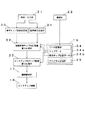
次に本発明の実施の形態を図面を参照して説明する。図1は本発明の一実施の形態のチップのピックアップ装置の構成を示すブロック図、図2は本発明の一実施の形態のチップのピックアップ装置のピックアップ対象となるウェハ治具の平面図、図3は本発明の一実施の形態のチップのピックアップ装置におけるウェハ治具の位置参照処理機能を示す機能ブロック図、図4は本発明の一実施の形態のチップのピックアップ方法におけるマップデ
ータの説明図、図5は本発明の一実施の形態のチップのピックアップ方法におけるピックアップ処理フローを示す図、図6は本発明の一実施の形態のチップのピックアップ方法におけるウェハ治具の位置参照用の参照チップ設定の説明図、図7は本発明の一実施の形態のチップのピックアップ方法における参照チップの位置の自動検出の説明図である。
Next, embodiments of the present invention will be described with reference to the drawings. FIG. 1 is a block diagram showing the configuration of a chip pickup apparatus according to an embodiment of the present invention. FIG. 2 is a plan view of a wafer jig to be picked up by the chip pickup apparatus according to an embodiment of the present invention. 3 is a functional block diagram showing the position reference processing function of the wafer jig in the chip pickup apparatus of one embodiment of the present invention, and FIG. 4 is an explanatory diagram of map data in the chip pickup method of one embodiment of the present invention. FIG. 5 is a diagram showing a pick-up processing flow in the chip pick-up method according to the embodiment of the present invention. FIG. 6 is a reference chip for referring to the position of the wafer jig in the chip pick-up method according to the embodiment of the present invention. FIG. 7 is an explanatory diagram of setting, and FIG. 7 is an explanatory diagram of automatic detection of the position of the reference chip in the chip pickup method of one embodiment of the present invention.
まず図1を参照して、チップのピックアップ装置の構成を説明する。チップのピックアップ装置は、チップ保持治具に所定配列で保持されたチップを、チップ保持治具からピックアップする機能を有している。図1において、部品供給部1は、移動手段としてのXYテーブル2によって水平方向に移動自在な治具テーブル2aを備えている。治具テーブル2aはピックアップ装置の装置機械座標系と関連付けられて配置されており、治具テーブル2aには、図2に示すチップ保持治具であるウェハ治具3が装着保持される。ウェハ治具3は、半導体ウェハ5から個片に切り出された状態の半導体チップ5a(以下、単に「チップ5a」と略記。)を貼着保持したウェハシート4を、円環状のウェハリング3aに装着した構造となっている。
First, the configuration of a chip pickup device will be described with reference to FIG. The chip pickup device has a function of picking up the chips held in a predetermined arrangement on the chip holding jig from the chip holding jig. In FIG. 1, the
図2に示すように、チップ5aは半導体ウェハ5から格子配列(所定配列)で切り出された形態となっており、半導体ウェハ5の特定位置(ここでは左端側に位置する1つの格子線位置)には、半導体ウェハ5の位置を特定するための基準位置となるノッチ5bが形成されている。また、ウェハシート4において半導体ウェハ5の外側の余白部分には、ウェハ治具3を特定するための識別コードが印刷されたバーコードラベル23が貼付されている。
As shown in FIG. 2, the chip 5a is cut out from the
図1において、ウェハ治具3の下方にはエジェクタ機構6が配設されている。エジェクタ機構6は昇降自在なエジェクタピンを備えており、エジェクタピンを上昇させることによりウェハシート4を突き破って半導体ウェハ5を下面から突き上げ、ウェハシート4から剥離させる。ダイエジェクタ6の中心位置は、ピックアップヘッドであるピックアップ機構16のノズル16aによってチップ5aのピックアップを行うピックアップ位置と一致するよう予め調整されている。なお、ピックアップヘッドのみでチップ5aのピックアップを行うことが可能な場合(例えば部品トレイからピックアップする場合等)には、ダイエジェクタ6は使用する必要がない。
In FIG. 1, an
部品供給部1の上方には、カメラ8および光学系9を備えた撮像部7が配設されている。撮像部7は、治具テーブル2aに装着保持された状態のウェハ治具3上のチップ5aを撮像する撮像手段となっている。撮像された画像データは認識処理手段としての画像認識部11に送られ、ここでチップ5aの位置が認識される。この認識結果はチップ5aの位置情報として出力される。この位置情報に基づいてXYテーブル2を駆動することにより、チップ5aの中心をダイエジェクタ6の中心に合致させることができ、チップ5aはピックアップ機構16によるチップのピックアップ位置に位置合わせされる。
An
治具テーブル2aの上方には、ウェハ治具3においてバーコードラベル23が貼付された位置に対応して、読取ヘッド12aが配置されている。読取ヘッド12aがバーコードラベル23から読み取った信号をバーコード読取部12が処理することにより、バーコードラベル23の印刷された識別コード、すなわち個別のウェハ治具3を識別するための識別コードを読み取ることができる。
Above the jig table 2a, the read head 12a is arranged corresponding to the position where the
部品供給部1の側方には、基板位置決め部13が配設されている。搬送路14上を搬送された基板15はここで位置決めされる。ピックアップ機構16は、前述の位置認識により位置補正されダイエジェクタ6によって突上げられたチップ5aをピックアップして基板位置決め部13まで移送し、基板15上にボンディングする。したがってピックアップ機構16はチップ移載手段としても機能する。
A board positioning unit 13 is disposed on the side of the
次に制御系の構成について説明する。機構制御部17は、XYテーブル2、ダイエジェクタ6,ピックアップ機構16の動作を制御する。CPU18は全体制御部であり、ピックアップ動作やボンディング動作全体を制御するほか、後述する各種処理を実行するための演算を行う。記憶装置19はボンディング動作等、各種処理動作に必要なプログラムや、各種処理実行のためのデータを記憶する。
Next, the configuration of the control system will be described. The
表示モニタ20は、ティーチング時やデータ入力時の操作画面や、撮像部7によって撮像された画像を表示する。操作・入力部21は、キーボードや表示モニタ20の表示画面上のポインティングデバイス(タッチパネル)であり、操作時やティーチング時の入力を行う。通信部22は、ホストコンピュータなどの他装置とのデータ授受を行う。
The display monitor 20 displays an operation screen during teaching or data input, and an image captured by the
次に、図3を参照して、チップのピックアップ装置におけるウェハ治具の位置参照処理機能について説明する。なお、図3に示す参照チップ設定処理部30、座標教示処理部31、後続参照チップ対応座標算出処理部32、ピックアップ用チップ座標算出処理部33は、CPU18が記憶装置19のプログラム記憶部35に記憶された処理プログラムを実行することにより、実現される機能を示している。
Next, the position reference processing function of the wafer jig in the chip pickup device will be described with reference to FIG. Note that the reference chip setting processing unit 30, the coordinate teaching processing unit 31, the subsequent reference chip corresponding coordinate calculation processing unit 32, and the pickup chip coordinate calculation processing unit 33 shown in FIG. 3 are stored in the program storage unit 35 of the
まず、記憶装置19のデータ記憶部34に記憶されたマップデータ34aについて、図4を参照して説明する。マップデータ34aは、ピックアップ機構16によってチップ5aをウェハ治具3から取り出す際の、取り出すべきチップ5aの位置をマップとして示すデータである。マップデータ34aは前工程において実行された検査の結果に基づいて、個々のウェハ治具3ごとに当該ウェハ治具3を特定する識別コードと関連付けられて作成され、通信部22を介して受信されたマップデータ34aは記憶部34に記憶される。なお、マップデータ34aを記憶部34に記憶させる際には、必ずしも通信部22を介する必要はなく、マップデータ34aを記憶させたフレキシブルディスク、CD−ROMなどの記憶媒体を用いてもよい。
First, the map data 34a stored in the
図4において、半導体ウェハ5はx方向、y方向にそれぞれpx、pyのピッチでマトリクス状に分割されており、それぞれのセルが個片のチップ5aに対応している。ここでxy座標系はウェハ治具3における半導体ウェハ5に固有の直交座標系であり、この例では、ノッチ5bの位置を原点として設定されている。1,2,3・・およびI,II,III・・は、ウェハ治具3におけるチップ5aの配列の行位置、列位置をそれぞれ示すインデックスである。すなわち、ピッチpx、pyおよび行方向、列方向のインデックスは、ウェハ治具3におけるチップ5aの配列を特定する配列データであり、この配列データが与えられることによりウェハ治具3におけるチップ5aの配列状態を特定することができる。
In FIG. 4, a
これらの2つのインデックスの組み合わせにより特定されるセルのうち、半導体ウェハ5の内部に完全に包含されるもののみがチップ5aとして用いられ、さらにこれらのチップ5aのうち、検査の結果良品と判定されたチップ5aのみが選別されてウェハ治具3から取り出される。図4においては、○印が付されたセルに対応するチップ5aが良品を示しており、×印が付されたセルに対応するチップ5aはそのまま残置される不良品を示している。ウェハ治具3において各チップ5aに対応するセルに○×が付されたデータは、個々のチップ5aの良否を示す良否データとなっている。すなわちデータ記憶部34は、ウェハ治具3におけるチップ5aの配列を示す配列データおよび個々のチップの良否を示す良否データを含むマップデータを記憶するマップデータ記憶手段となっている。
Of the cells specified by the combination of these two indexes, only those completely contained within the
参照チップ設定処理部30は、操作・入力部21からの入力にしたがって、治具テーブル2aの装置機械座標系における位置を特定するための参照用に用いられる複数の参照チ
ップを設定する処理を行う。すなわち、表示モニタ20に図4に示すマップデータを表示させ、この表示画面上で操作・入力部21の指示入力機能を用いて該当するチップ5aを指示することにより、図6に示すように、複数の参照チップ(R1,R2,R3)が設定される。
The reference chip setting processing unit 30 performs a process of setting a plurality of reference chips used for reference for specifying the position of the jig table 2a in the machine machine coordinate system in accordance with an input from the operation / input unit 21. . That is, by displaying the map data shown in FIG. 4 on the display monitor 20 and instructing the corresponding chip 5a using the instruction input function of the operation / input unit 21 on this display screen, as shown in FIG. A plurality of reference chips (R1, R2, R3) are set.
ここではまずノッチ5bに隣接して第1の参照チップR1が設定され、また第1の参照チップR1から略等しく離れた位置に第2の参照チップR2,第3の参照チップR3が設定される。なお位置参照用としては最小限2点の参照用チップを設定すれば足りるが、位置精度を向上させるためには3点の参照チップを設定することが望ましい。 Here, the first reference chip R1 is first set adjacent to the notch 5b, and the second reference chip R2 and the third reference chip R3 are set at positions substantially equal to the first reference chip R1. . Although it is sufficient to set at least two reference chips for position reference, it is desirable to set three reference chips in order to improve position accuracy.
このようにして設定された参照チップの位置情報は、以下に説明する後続参照チップ対応座標算出処理部32に対して提供される。すなわち、参照チップ設定処理部30は、チップ保持治具の前記装置機械座標系における位置を特定するための参照用に用いられる複数の参照チップの配列データにおける位置を参照チップ位置として提供する参照チップ位置提供手段となっている。また参照チップ設定処理部30は、データ記憶部34から読み出され表示モニタ20に表示された配列データ上で複数の参照チップを指定入力するデータ入力手段としても機能する。
The reference chip position information set in this way is provided to the subsequent reference chip corresponding coordinate calculation processing unit 32 described below. That is, the reference chip setting processing unit 30 provides the position in the array data of a plurality of reference chips used for reference for specifying the position of the chip holding jig in the apparatus machine coordinate system as the reference chip position. It is a location providing means. The reference chip setting processing unit 30 also functions as data input means for designating and inputting a plurality of reference chips on the array data read from the
なお、参照チップ設定処理部30によって参照チップ位置を表示モニタ20上でその都度設定する替わりに、第1の参照チップR1、第2の参照チップR2、第3の参照チップR3の位置を示すデータ(図6に示す例では、(1,IV)、(5,VI)、(6、II))を、参照チップ位置データ34bとしてデータ記憶部34に予め記憶させておき、後続参照チップ対応座標算出処理部32に参照チップ位置データ34bを送ることにより参照チップ位置を提供するようにしてもよい。この場合には、データ記憶部34が、複数の参照チップの配列データにおける位置を参照チップ位置として提供する参照チップ位置提供手段となる。
Data indicating the positions of the first reference chip R1, the second reference chip R2, and the third reference chip R3 instead of setting the reference chip position on the display monitor 20 each time by the reference chip setting processing unit 30. ((1, IV), (5, VI), (6, II) in the example shown in FIG. 6) is stored in advance in the
座標教示処理部31は、表示モニタ20に表示された画面上で操作・入力部21によって特定位置を指示入力することにより、当該位置の装置機械座標系における位置座標を教示するいわゆる位置ティーチング処理を行う。この位置ティーチング処理により、参照チップ設定処理部30によって設定された複数の参照チップのうち、最初に参照される第1の参照チップの位置を装置機械座標系における第1参照チップ対応座標として教示する処理が行われる。すなわち、座標教示処理部31は、治具テーブル2aに装着保持されたウェハシート4において、複数の参照チップのうち最初に参照される第1の参照チップに対応する位置座標を第1参照チップ対応座標として教示する座標教示手段となっている。
The coordinate teaching processing unit 31 performs a so-called position teaching process for teaching a position coordinate in the machine-machine coordinate system of the position by instructing and inputting a specific position by the operation / input unit 21 on the screen displayed on the display monitor 20. Do. By this position teaching process, the position of the first reference chip that is first referred to among the plurality of reference chips set by the reference chip setting processing unit 30 is taught as the coordinates corresponding to the first reference chip in the apparatus machine coordinate system. Processing is performed. That is, the coordinate teaching processing unit 31 sets the position coordinates corresponding to the first reference chip first referred to among the plurality of reference chips on the
後続参照チップ対応座標算出処理部32は、データ記憶部34から読み出されたマップデータ34aに含まれるチップ5aの配列データ、参照チップ設定処理部30によって設定された参照チップ位置および座標教示処理部31によって教示された第1参照チップ対応座標に基づいて、第2の参照チップR2、第3の参照チップR3の位置座標を後続参照チップ対応座標として算出する処理を行う。したがって、後続参照チップ対応座標算出処理部32は、配列データ、参照チップ位置および第1参照チップ対応座標に基づいて、被装着チップ保持治具である治具テーブル2a上のウェハ治具3において、第1の参照チップR1の後続参照チップに対応する位置座標を後続参照チップ対応座標として算出する後続参照チップ対応座標算出手段となっている。
The subsequent reference chip corresponding coordinate calculation processing unit 32 includes the array data of the chip 5 a included in the map data 34 a read from the
ピックアップ用チップ座標算出処理部33は、マップデータ34aに含まれるチップ5aの配列データ、第1の参照チップR1、第2の参照チップR2、第3の参照チップR3の装置機械座標系における位置座標に基づいて、半導体ウェハ5の各チップ5aの装置機械座標系における位置座標、すなわちピックアップ機構16によってチップ5aを取り出
す際のピックアップ用位置座標を、座標変換演算によって算出する。
The pick-up chip coordinate calculation processing unit 33 includes the arrangement data of the chips 5a included in the map data 34a, the position coordinates of the first reference chip R1, the second reference chip R2, and the third reference chip R3 in the apparatus machine coordinate system. Based on the above, the position coordinates in the apparatus machine coordinate system of each chip 5a of the
したがってピックアップ用チップ座標算出処理部33は、座標教示処理部31によって教示された第1参照チップ対応座標、後続参照チップ対応座標算出処理部32によって算出された後続参照チップ対応座標および参照チップ設定処理部30によって設定された参照チップ位置とに基づいて、被装着チップ保持治具であるウェハ治具3に保持された各チップ5aの装置機械座標系における位置座標を、ピックアップ位置として算出するピックアップ用チップ座標算出手段となっている。
Accordingly, the pick-up chip coordinate calculation processing unit 33 performs the first reference chip corresponding coordinates taught by the coordinate teaching processing unit 31, the subsequent reference chip corresponding coordinates calculated by the subsequent reference chip corresponding coordinate calculation processing unit 32, and the reference chip setting process. Based on the reference chip position set by the unit 30, the position coordinate in the apparatus machine coordinate system of each chip 5a held by the
算出された位置座標のデータは機構制御部17に送られ、機構制御部17がこの位置座標に基づいてピックアップ機構16を制御することにより、ピックアップ機構16は治具テーブル2a上のウェハ治具3からチップ5aをピックアップする。即ち、ピックアップ機構16および機構制御部17は、ピックアップ位置および良否データとに基づいて、ウェハ治具3から良品のチップ5aをピックアップするピックアップ手段となっている。
The calculated position coordinate data is sent to the
次に、図5を参照して、このチップのピックアップ装置によるチップのピックアップ処理フローについて説明する。このチップのピックアップ処理は、ウェハ治具3に所定配列で保持されたチップ5aをウェハ治具3からピックアップするものである。このピックアップ作業に先立って、ウェハ治具3におけるチップ5aの配列を示す配列データおよび前工程で実行された良否検査の結果を示す良否データを含むマップデータが通信部22を介して受信され、記憶部34に記憶されている。そしてピックアップの開始に際しては、まず上述のマップデータ34aをデータ記憶部34から読み出し(マップデータ読み出し工程)、ピックアップ作業の対象となるウェハ治具3のマップデータ34を表示モニタ20に表示させる(ST1)。
Next, a chip pick-up processing flow by the chip pick-up device will be described with reference to FIG. This chip pick-up process is to pick up the chips 5 a held in a predetermined arrangement on the
次いで、表示モニタ20に表示された配列データ上で、複数の参照チップ(R1,R2,R3)を指定入力する(ST2)。これにより、ウェハ治具3の装置機械座標系における位置を特定するための参照用に用いられる複数の参照チップ(R1,R2,R3)の配列データにおける位置が、参照チップ位置として提供される(参照チップ位置提供工程)。すなわち参照チップ位置提供工程においては、マップデータ読み出し工程にて読み出され表示モニタ20に表示された配列データ上で、複数の参照チップ(R1,R2,R3)を指定入力するようにしている。
Next, a plurality of reference chips (R1, R2, R3) are designated and input on the array data displayed on the display monitor 20 (ST2). Thereby, the position in the arrangement data of the plurality of reference chips (R1, R2, R3) used for reference for specifying the position of the
これと並行して、装置機械座標系と関連づけられて配置された治具テーブル2aにチップ保持治具であるウェハ治具3を装着保持させる(チップ保持治具装着工程)(ST3)。そして装着保持されたウェハ治具3に貼着されたバーコードラベル23を読み取ることによって当該ウェハ治具3を識別し、このウェハ治具3と既に読み出されたマップデータ34aとの照合を行う。なお、治具テーブル2aにウェハ治具3を装着する前にウェハ治具3の識別を行い、ウェハ治具3とマップデータ34aの照合を行うようにしてもよい。
In parallel with this, the
次いで、治具テーブルに装着保持された被装着チップ保持治具であるウェハ治具3において、複数の参照チップ(R1,R2,R3)のうち最初に参照される第1の参照チップR1に対応する位置座標を、座標教示処理部31によって第1参照チップ対応座標として教示する(座標教示工程)(ST4)。ここで、第1の参照チップR1は半導体ウェハ5においてノッチ5bに隣接して設定されていることから、オペレータが手動操作によって位置教示を行う際に第1の参照チップR1を容易に見いだすことができ、教示作業を確実に行うことができる。
Next, in the
次に、後続参照チップ(第2の参照チップR2、第3の参照チップR3)の位置を、画像認識によって自動探索することにより、後続参照チップに対応する位置座標を算出する
(ST5)。図7に示すように、まず治具テーブル2aに装着保持された複数のチップ5aのうち、(ST4)にて教示されたチップ位置をカメラ8に位置合わせする。そしてこの後、既知の参照チップ位置に基づき第2の参照チップR2、第3の参照チップR3を順次自動検出する。すなわち、第1の参照チップR1を認識起点として、順次隣接するチップ5aを撮像して位置認識し、撮像視野内におけるチップ5aの位置ずれを補正しながら、第2の参照チップR2に到達する。次いで第2の参照チップR2を認識起点として、同様に順次隣接するチップ5aを撮像して位置認識し、第3の参照チップR3に到達する。
Next, the position coordinates corresponding to the subsequent reference chip are calculated by automatically searching the position of the subsequent reference chip (second reference chip R2, third reference chip R3) by image recognition (ST5). As shown in FIG. 7, first, among the plurality of chips 5a mounted and held on the jig table 2a, the chip position taught in (ST4) is aligned with the
すなわちここでは、撮像手段であるカメラ8を治具テーブル2a上のウェハ治具3に対して相対移動させながらチップ5aを順次撮像して撮像結果を認識処理することによりチップを検出するチップ認識処理を、後続参照チップを検出するまで繰り返す自動認識処理を行う。この自動認識処理により、配列データ、参照チップ位置および第1参照チップ対応座標に基づいて、ウェハ治具3において第1の参照チップR1以外の後続参照チップである第2の参照チップR2、第3の参照チップR3に対応する位置座標が、後続参照チップ対応座標として算出される(後続参照チップ対応座標算出工程)。なお、上記自動認識処理は、必ずしも隣接するチップに対して行う必要はなく、1つおき、5つおきなど、適宜チップをスキップして行ってもよい。
That is, here, chip recognition processing for detecting a chip by sequentially imaging the chip 5a and recognizing the imaging result while moving the
次に第1参照チップ対応座標、後続参照チップ対応座標および参照チップ位置とに基づいて、ウェハ3に保持された各チップ5aの装置機械座標系における位置座標をピックアップ用チップ座標(ピックアップ位置)として算出する(ピックアップ用チップ座標算出工程)。すなわち、図7に示すように、当初ウェハシート4に固有のxy座標系にて与えられていた第1の参照チップR1、第2の参照チップR2、第3の参照チップR3の位置が、装置機械座標系(XY座標系)における座標位置として与えられることにより、xy座標系をXY座標系に座標変換するための座標変換データが求められる。
Next, based on the coordinates corresponding to the first reference chip, the coordinates corresponding to the subsequent reference chip, and the reference chip position, the position coordinates in the apparatus machine coordinate system of each chip 5a held on the
これにより、半導体ウェハ5の各チップ5aの位置座標を、装置機械座標系における位置座標に変換することが可能となる。そしてこのようにして求められたピックアップ用チップ座標およびマップデータに含まれるチップの良否データとに基づいて、ウェハ治具3から良品のチップ5aをピックアップする(ピックアップ工程)。
As a result, the position coordinates of each chip 5a of the
上記説明したように、本実施の形態に示すチップのピックアップにおいては、治具テーブル2aに装着保持されたウェハシート4において位置参照用に設定された複数の参照チップのうち、最初に参照される第1の参照チップR1の位置座標のみをオペレータによる位置ティーチング操作によって第1参照チップ対応座標として教示し、第1の参照チップR1以外の後続参照チップに対応する位置座標を、画像認識を用いた自動認識によって演算して求めるようにしている。
As described above, in the chip pickup shown in the present embodiment, reference is first made among a plurality of reference chips set for position reference on the
これにより、通常のチップを参照チップとして設定し、参照チップの位置を画像認識による自動検出やマニュアルによるティーチングによって求める際に従来より課題とされていた問題点を解消することが可能となっている。すなわち全ての参照用チップを自動認識により検出する場合において、小サイズチップを対象とする場合に発生しやすい誤検出、例えば本来参照用チップとして設定されたチップに隣接するチップを誤って検出することによる不具合が発生しない。 As a result, it is possible to set a normal chip as a reference chip, and to solve the problems that have been a problem in the past when the position of the reference chip is obtained by automatic detection by image recognition or manual teaching. . That is, when all the reference chips are detected by automatic recognition, erroneous detection that is likely to occur when targeting a small-sized chip, for example, erroneously detecting a chip adjacent to a chip originally set as a reference chip Does not cause malfunction.
また、本実施の形態に示す例では、最初に参照される第1の参照チップR1を半導体ウェハ5の基準位置を示すノッチ5bに隣接して設定していることから、第1の参照チップR1の位置を容易且つ正確に教示することができ、ティーチングに際しての人為的ミスの発生を有効に防止することができる。したがって、先行技術例に示すように専用の位置参照用のチップを作り込む方法と比較して、工程コストの増大や製品歩留まりの低下を招く
ことなく、参照チップの位置検出を低コストで効率よく行うことが可能となっている。
In the example shown in the present embodiment, the first reference chip R1 that is referred to first is set adjacent to the notch 5b that indicates the reference position of the
なお、低コストというメリットは低下するものの、先行技術に示したような専用の位置参照用のチップを作り込んだチップ保持治具に対しても、本発明は適用可能である。 Although the merit of low cost is reduced, the present invention can be applied to a chip holding jig in which a dedicated position reference chip as shown in the prior art is formed.
本発明のチップのピックアップ装置およびチップのピックアップ方法は、チップ保持治具におけるチップの位置検出を低コストで効率よく行うことができる。という効果を有し、ウェハ治具からチップを個片状態で取り出すダイボンディング装置に有用である。 The chip pickup apparatus and chip pickup method of the present invention can efficiently detect the position of a chip in a chip holding jig at a low cost. It is useful for a die bonding apparatus that takes out chips in a single piece from a wafer jig.
1 部品供給部
2a 治具テーブル
3 ウェハ治具
4 ウェハシート
5 半導体ウェハ
5a 半導体チップ(チップ)
8 カメラ
R1 第1の参照チップ
R2 第2の参照チップ
R3 第3の参照チップ
DESCRIPTION OF
8 Camera R1 First reference chip R2 Second reference chip R3 Third reference chip
Claims (4)
前記チップ保持治具を装着保持し装置機械座標系と関連づけられて配置された治具テーブルと、前記チップ保持治具における前記チップの配列を示す配列データおよび個々のチップの良否を示す良否データを含むマップデータを記憶するマップデータ記憶手段と、
前記チップ保持治具の前記装置機械座標系における位置を特定するための参照用に用いられる複数の参照チップの前記配列データにおける位置を参照チップ位置として提供する参照チップ位置提供手段と、
前記治具テーブルに装着保持された被装着チップ保持治具において、前記複数の参照チップのうち最初に参照される第1の参照チップに対応する位置座標を第1参照チップ対応座標として教示する座標教示手段と、
前記被装着チップ保持治具上のチップを撮像する撮像手段と、前記撮像手段を前記被装着チップ保持治具に対して相対移動させる移動手段と、前記撮像手段による撮像結果を認識処理して前記チップを検出する認識処理手段とを含むチップ認識手段を備え、前記撮像手段を前記被装着チップ保持治具に対して相対移動させながら前記チップを順次撮像して撮像結果を認識処理することにより前記チップを検出するチップ認識処理を、後続参照チップを検出するまで繰り返す自動認識処理を行い、この自動認識処理により、前記配列データ、前記参照チップ位置および前記第1参照チップ対応座標に基づいて、前記被装着チップ保持治具において前記第1の参照チップ以外の後続参照チップに対応する位置座標を後続参照チップ対応座標として算出する後続参照チップ対応座標算出手段と、
前記第1参照チップ対応座標、前記後続参照チップ対応座標および前記参照チップ位置とに基づいて、前記被装着チップ保持治具に保持された各チップの前記装置機械座標系における位置座標をピックアップ位置として算出するピックアップ用チップ座標算出手段と、
前記ピックアップ位置および前記良否データとに基づいて、前記被装着チップ保持治具から良品のチップをピックアップするピックアップ手段とを備えたことを特徴とするチップのピックアップ装置。 A chip pickup device for picking up chips held in a predetermined arrangement on a chip holding jig from the chip holding jig,
A jig table that is mounted and held in association with the machine machine coordinate system and that has the chip holding jig, arrangement data indicating the arrangement of the chips in the chip holding jig, and pass / fail data indicating pass / fail of individual chips. Map data storage means for storing map data including;
Reference chip position providing means for providing, as reference chip positions, positions in the array data of a plurality of reference chips used for reference for specifying positions in the apparatus machine coordinate system of the chip holding jig;
In the mounted chip holding jig mounted and held on the jig table, the coordinates that teach the position coordinates corresponding to the first reference chip that is first referred to as the first reference chip corresponding coordinates among the plurality of reference chips. Teaching means;
An imaging unit for imaging a chip on the mounted chip holding jig, a moving unit for moving the imaging unit relative to the mounted chip holding jig, and an imaging result obtained by the imaging unit for recognition processing. A chip recognition means including a recognition processing means for detecting a chip, and sequentially picking up the chips while reciprocally moving the image pickup means with respect to the mounted chip holding jig, thereby performing recognition processing of the image pickup results. A chip recognition process for detecting a chip is repeated until a subsequent reference chip is detected. By this automatic recognition process, based on the array data, the reference chip position, and the coordinates corresponding to the first reference chip, Position coordinates corresponding to subsequent reference chips other than the first reference chip in the mounted chip holding jig are coordinates corresponding to subsequent reference chips. And subsequent reference chip corresponding coordinates calculation means for output,
Based on the coordinates corresponding to the first reference chip, the coordinates corresponding to the subsequent reference chip, and the reference chip position, the position coordinate in the apparatus machine coordinate system of each chip held by the mounted chip holding jig is used as the pickup position. Pick-up chip coordinate calculating means for calculating;
A chip pickup device comprising: pickup means for picking up a non-defective chip from the mounted chip holding jig based on the pickup position and the pass / fail data.
前記チップ保持治具における前記チップの配列を示す配列データおよび個々のチップの良否を示す良否データを含むマップデータを読み出すマップデータ読み出し工程と、
前記チップ保持治具の前記装置機械座標系における位置を特定するための参照用に用いられる複数の参照チップの前記配列データにおける位置を参照チップ位置として提供する参照チップ位置提供工程と、
装置機械座標系と関連づけられて配置された治具テーブルに前記チップ保持治具を装着保持させるチップ保持治具装着工程と、
前記治具テーブルに装着保持された被装着チップ保持治具において、前記複数の参照チップのうち最初に参照される第1の参照チップに対応する位置座標を第1参照チップ対応座標として教示する座標教示工程と、
撮像手段を前記被装着チップ保持治具に対して相対移動させながら前記チップを順次撮像して撮像結果を認識処理することにより前記チップを検出するチップ認識処理を、後続参照チップを検出するまで繰り返す自動認識処理を行い、この自動認識処理により、前記配列データ、前記参照チップ位置および前記第1参照チップ対応座標に基づいて、前記被装着チップ保持治具において前記第1の参照チップ以外の後続参照チップに対応する位置座標を後続参照チップ対応座標として算出する後続参照チップ対応座標算出工程と、
前記第1参照チップ対応座標、前記後続参照チップ対応座標および前記参照チップ位置とに基づいて、前記被装着チップ保持治具に保持された各チップの前記装置機械座標系における位置座標をピックアップ位置として算出するピックアップ用チップ座標算出工程と、
前記ピックアップ位置および前記良否データとに基づいて、前記被装着チップ保持治具から良品のチップをピックアップするピックアップ工程とを含むことを特徴とするチップのピックアップ方法。 A chip pickup method for picking up chips held in a predetermined arrangement on a chip holding jig from the chip holding jig,
A map data reading step of reading out map data including arrangement data indicating the arrangement of the chips in the chip holding jig and pass / fail data indicating pass / fail of each chip;
A reference chip position providing step of providing, as reference chip positions, positions in the array data of a plurality of reference chips used for reference for specifying positions in the device machine coordinate system of the chip holding jig;
A chip holding jig mounting step for mounting and holding the chip holding jig on a jig table arranged in association with the apparatus machine coordinate system;
In the mounted chip holding jig mounted and held on the jig table, the coordinates that teach the position coordinates corresponding to the first reference chip that is first referred to as the first reference chip corresponding coordinates among the plurality of reference chips. Teaching process;
The chip recognition process for detecting the chip by sequentially imaging the chips and recognizing the imaging result while moving the imaging means relative to the mounted chip holding jig is repeated until a subsequent reference chip is detected. performs automatic recognition processing by the automatic recognition process, the sequence data, the reference on the basis of the chip position and the first reference chip corresponding coordinate subsequent reference other than the first reference chip in said mating attachment chip holding jig A subsequent reference chip corresponding coordinate calculating step of calculating a position coordinate corresponding to the chip as a subsequent reference chip corresponding coordinate;
Based on the coordinates corresponding to the first reference chip, the coordinates corresponding to the subsequent reference chip, and the reference chip position, the position coordinate in the apparatus machine coordinate system of each chip held by the mounted chip holding jig is used as the pickup position. A chip coordinate calculation step for the pickup to calculate,
A chip pick-up method comprising: a pick-up step of picking up a non-defective chip from the mounted chip holding jig based on the pick-up position and the pass / fail data.
Priority Applications (1)
| Application Number | Priority Date | Filing Date | Title |
|---|---|---|---|
| JP2005155284A JP4507985B2 (en) | 2005-05-27 | 2005-05-27 | Chip pickup device and pickup method |
Applications Claiming Priority (1)
| Application Number | Priority Date | Filing Date | Title |
|---|---|---|---|
| JP2005155284A JP4507985B2 (en) | 2005-05-27 | 2005-05-27 | Chip pickup device and pickup method |
Publications (2)
| Publication Number | Publication Date |
|---|---|
| JP2006332417A JP2006332417A (en) | 2006-12-07 |
| JP4507985B2 true JP4507985B2 (en) | 2010-07-21 |
Family
ID=37553776
Family Applications (1)
| Application Number | Title | Priority Date | Filing Date |
|---|---|---|---|
| JP2005155284A Active JP4507985B2 (en) | 2005-05-27 | 2005-05-27 | Chip pickup device and pickup method |
Country Status (1)
| Country | Link |
|---|---|
| JP (1) | JP4507985B2 (en) |
Cited By (1)
| Publication number | Priority date | Publication date | Assignee | Title |
|---|---|---|---|---|
| CN110335846A (en) * | 2019-06-26 | 2019-10-15 | 青岛航天半导体研究所有限公司 | Chip tightens the device and method picked manually |
Families Citing this family (15)
| Publication number | Priority date | Publication date | Assignee | Title |
|---|---|---|---|---|
| JP5007137B2 (en) * | 2007-03-29 | 2012-08-22 | 株式会社日立ハイテクインスツルメンツ | Electronic component pickup device and taping device |
| JP2010192817A (en) * | 2009-02-20 | 2010-09-02 | Canon Machinery Inc | Pickup method and pickup device |
| JP5721476B2 (en) * | 2011-03-09 | 2015-05-20 | 富士機械製造株式会社 | Electronic component mounting apparatus and electronic component mounting method |
| TWI498993B (en) * | 2011-11-09 | 2015-09-01 | I Hsing Tsai | Method for automatically positioning first die on wafer |
| CN103117207B (en) * | 2011-11-16 | 2015-08-19 | 蔡宜兴 | The automatic positioning method of first crystal grain |
| EP2833395B1 (en) * | 2012-03-27 | 2019-05-01 | FUJI Corporation | Die supply device |
| JP5614825B1 (en) * | 2013-11-29 | 2014-10-29 | 上野精機株式会社 | Classification device, classification method, and classification program |
| KR102189285B1 (en) * | 2014-11-04 | 2020-12-09 | 세메스 주식회사 | Method of obtaining location information of dies |
| US9633883B2 (en) | 2015-03-20 | 2017-04-25 | Rohinni, LLC | Apparatus for transfer of semiconductor devices |
| KR102618804B1 (en) * | 2016-05-24 | 2023-12-27 | 세메스 주식회사 | Method of forming a recipe of a die bonging process |
| US10141215B2 (en) | 2016-11-03 | 2018-11-27 | Rohinni, LLC | Compliant needle for direct transfer of semiconductor devices |
| US10504767B2 (en) | 2016-11-23 | 2019-12-10 | Rohinni, LLC | Direct transfer apparatus for a pattern array of semiconductor device die |
| JP6858452B2 (en) * | 2017-06-23 | 2021-04-14 | 株式会社ディスコ | Wafer jig with identification mark |
| US11094571B2 (en) | 2018-09-28 | 2021-08-17 | Rohinni, LLC | Apparatus to increase transferspeed of semiconductor devices with micro-adjustment |
| CN112992752B (en) * | 2021-03-04 | 2023-01-13 | 深圳源明杰科技股份有限公司 | Wafer map display method, system, equipment and storage medium |
Citations (1)
| Publication number | Priority date | Publication date | Assignee | Title |
|---|---|---|---|---|
| JP2002026041A (en) * | 2000-07-12 | 2002-01-25 | Nec Machinery Corp | Die bonder |
-
2005
- 2005-05-27 JP JP2005155284A patent/JP4507985B2/en active Active
Patent Citations (1)
| Publication number | Priority date | Publication date | Assignee | Title |
|---|---|---|---|---|
| JP2002026041A (en) * | 2000-07-12 | 2002-01-25 | Nec Machinery Corp | Die bonder |
Cited By (2)
| Publication number | Priority date | Publication date | Assignee | Title |
|---|---|---|---|---|
| CN110335846A (en) * | 2019-06-26 | 2019-10-15 | 青岛航天半导体研究所有限公司 | Chip tightens the device and method picked manually |
| CN110335846B (en) * | 2019-06-26 | 2021-05-11 | 青岛航天半导体研究所有限公司 | Chip tightening manual picking device |
Also Published As
| Publication number | Publication date |
|---|---|
| JP2006332417A (en) | 2006-12-07 |
Similar Documents
| Publication | Publication Date | Title |
|---|---|---|
| JP4507985B2 (en) | Chip pickup device and pickup method | |
| KR100598787B1 (en) | Improved method and apparatus for direct probe sensing | |
| EP1666185B1 (en) | Laser processing machine and method with image acquisition and processing means | |
| JP2015159294A (en) | Wafer handler comprising vision system | |
| US20120197427A1 (en) | Apparatus For Cutting Amd/or Etching Articles Comprising A Flat Surface On Which Designs And/or Writings Are Reproduced And A method For Actuating The Apparatus | |
| US20080151234A1 (en) | Foreign matter inspection apparatus | |
| WO2015001599A1 (en) | Feeder adjusting device | |
| CN111656504A (en) | Die picking method and device | |
| JP4979989B2 (en) | Chip mounting apparatus and mounting method | |
| JP5941715B2 (en) | DIE PICKUP DEVICE AND DIE PICKUP METHOD | |
| JP2013004794A (en) | Pickup device of semiconductor chip, pickup method, die bonding device, die bonding method and method of manufacturing semiconductor device | |
| JP4122170B2 (en) | Component mounting method and component mounting apparatus | |
| US10069042B2 (en) | Light-emitting components containing body, manufacturing method of light-emitting components containing body, components mounting apparatus, components mounting method, and components mounting system | |
| WO2018158888A1 (en) | Backup-pin recognizing method and component mounting device | |
| JP2010212358A (en) | Method of manufacturing semiconductor device | |
| JP4927776B2 (en) | Component mounting method | |
| JP4913720B2 (en) | Electronic component mounting method for electronic component mounting apparatus | |
| CN111492726B (en) | Tracking device | |
| JP5243284B2 (en) | Correction position detection apparatus, correction position detection method, and bonding apparatus | |
| JP2913609B2 (en) | Probing apparatus, probing method and probe card | |
| JP4973630B2 (en) | Nozzle identification device, component mounting machine, nozzle identification method, and component mounting method | |
| JP2010192817A (en) | Pickup method and pickup device | |
| JP4421281B2 (en) | Component recognition method, component recognition device, surface mounter, component test device, and board inspection device | |
| TWI400020B (en) | Picking-up and placing method with integrated pcb information | |
| JP6086671B2 (en) | Die component supply device |
Legal Events
| Date | Code | Title | Description |
|---|---|---|---|
| A621 | Written request for application examination |
Free format text: JAPANESE INTERMEDIATE CODE: A621 Effective date: 20070326 |
|
| RD01 | Notification of change of attorney |
Free format text: JAPANESE INTERMEDIATE CODE: A7421 Effective date: 20070412 |
|
| RD01 | Notification of change of attorney |
Free format text: JAPANESE INTERMEDIATE CODE: A7421 Effective date: 20091126 |
|
| A131 | Notification of reasons for refusal |
Free format text: JAPANESE INTERMEDIATE CODE: A131 Effective date: 20091201 |
|
| A521 | Written amendment |
Free format text: JAPANESE INTERMEDIATE CODE: A523 Effective date: 20100121 |
|
| TRDD | Decision of grant or rejection written | ||
| A01 | Written decision to grant a patent or to grant a registration (utility model) |
Free format text: JAPANESE INTERMEDIATE CODE: A01 Effective date: 20100413 |
|
| A01 | Written decision to grant a patent or to grant a registration (utility model) |
Free format text: JAPANESE INTERMEDIATE CODE: A01 |
|
| A61 | First payment of annual fees (during grant procedure) |
Free format text: JAPANESE INTERMEDIATE CODE: A61 Effective date: 20100426 |
|
| FPAY | Renewal fee payment (event date is renewal date of database) |
Free format text: PAYMENT UNTIL: 20130514 Year of fee payment: 3 |
|
| R151 | Written notification of patent or utility model registration |
Ref document number: 4507985 Country of ref document: JP Free format text: JAPANESE INTERMEDIATE CODE: R151 |
|
| FPAY | Renewal fee payment (event date is renewal date of database) |
Free format text: PAYMENT UNTIL: 20130514 Year of fee payment: 3 |
|
| FPAY | Renewal fee payment (event date is renewal date of database) |
Free format text: PAYMENT UNTIL: 20130514 Year of fee payment: 3 |