JP4416901B2 - Level shifter - Google Patents
Level shifter Download PDFInfo
- Publication number
- JP4416901B2 JP4416901B2 JP2000071256A JP2000071256A JP4416901B2 JP 4416901 B2 JP4416901 B2 JP 4416901B2 JP 2000071256 A JP2000071256 A JP 2000071256A JP 2000071256 A JP2000071256 A JP 2000071256A JP 4416901 B2 JP4416901 B2 JP 4416901B2
- Authority
- JP
- Japan
- Prior art keywords
- mos transistor
- drain
- electrically connected
- source
- gate
- Prior art date
- Legal status (The legal status is an assumption and is not a legal conclusion. Google has not performed a legal analysis and makes no representation as to the accuracy of the status listed.)
- Expired - Fee Related
Links
Images


Classifications
-
- H—ELECTRICITY
- H03—ELECTRONIC CIRCUITRY
- H03K—PULSE TECHNIQUE
- H03K3/00—Circuits for generating electric pulses; Monostable, bistable or multistable circuits
- H03K3/02—Generators characterised by the type of circuit or by the means used for producing pulses
- H03K3/353—Generators characterised by the type of circuit or by the means used for producing pulses by the use, as active elements, of field-effect transistors with internal or external positive feedback
- H03K3/356—Bistable circuits
-
- H—ELECTRICITY
- H03—ELECTRONIC CIRCUITRY
- H03K—PULSE TECHNIQUE
- H03K19/00—Logic circuits, i.e. having at least two inputs acting on one output; Inverting circuits
- H03K19/0008—Arrangements for reducing power consumption
- H03K19/0013—Arrangements for reducing power consumption in field effect transistor circuits
-
- H—ELECTRICITY
- H03—ELECTRONIC CIRCUITRY
- H03K—PULSE TECHNIQUE
- H03K19/00—Logic circuits, i.e. having at least two inputs acting on one output; Inverting circuits
- H03K19/0175—Coupling arrangements; Interface arrangements
- H03K19/0185—Coupling arrangements; Interface arrangements using field effect transistors only
- H03K19/018507—Interface arrangements
- H03K19/018521—Interface arrangements of complementary type, e.g. CMOS
-
- G—PHYSICS
- G09—EDUCATION; CRYPTOGRAPHY; DISPLAY; ADVERTISING; SEALS
- G09G—ARRANGEMENTS OR CIRCUITS FOR CONTROL OF INDICATING DEVICES USING STATIC MEANS TO PRESENT VARIABLE INFORMATION
- G09G2310/00—Command of the display device
- G09G2310/02—Addressing, scanning or driving the display screen or processing steps related thereto
- G09G2310/0264—Details of driving circuits
- G09G2310/0289—Details of voltage level shifters arranged for use in a driving circuit
-
- G—PHYSICS
- G09—EDUCATION; CRYPTOGRAPHY; DISPLAY; ADVERTISING; SEALS
- G09G—ARRANGEMENTS OR CIRCUITS FOR CONTROL OF INDICATING DEVICES USING STATIC MEANS TO PRESENT VARIABLE INFORMATION
- G09G3/00—Control arrangements or circuits, of interest only in connection with visual indicators other than cathode-ray tubes
- G09G3/20—Control arrangements or circuits, of interest only in connection with visual indicators other than cathode-ray tubes for presentation of an assembly of a number of characters, e.g. a page, by composing the assembly by combination of individual elements arranged in a matrix no fixed position being assigned to or needed to be assigned to the individual characters or partial characters
- G09G3/34—Control arrangements or circuits, of interest only in connection with visual indicators other than cathode-ray tubes for presentation of an assembly of a number of characters, e.g. a page, by composing the assembly by combination of individual elements arranged in a matrix no fixed position being assigned to or needed to be assigned to the individual characters or partial characters by control of light from an independent source
- G09G3/36—Control arrangements or circuits, of interest only in connection with visual indicators other than cathode-ray tubes for presentation of an assembly of a number of characters, e.g. a page, by composing the assembly by combination of individual elements arranged in a matrix no fixed position being assigned to or needed to be assigned to the individual characters or partial characters by control of light from an independent source using liquid crystals
- G09G3/3611—Control of matrices with row and column drivers
- G09G3/3685—Details of drivers for data electrodes
- G09G3/3688—Details of drivers for data electrodes suitable for active matrices only
Description
【0001】
【発明の属する技術分野】
【0002】
本発明は、マトリクス状に配置されたスイッチング素子と画素により映像などの情報の表示を行なう画像表示装置(アクティブマトリクス型画像表示装置)の駆動回路に用いられるレベルシフタに関する。
【0003】
【従来の技術】
近年、半導体製造技術の微細化が進み、また、携帯機器用LSIなどのように低消費電力が要求されるようになり3.3Vといった低電源電圧駆動のLSIが主流になっている。
【0004】
一方で、携帯端末やコンピューター用モニターなどの用途として最近需要が高い液晶ディスプレイは、液晶駆動を10〜20Vの電圧振幅の信号で行うことから、その駆動回路には対応する高電源電圧で動作する回路部が少なくとも存在する。
【0005】
従って、コントローラーLSIの低電圧振幅信号と液晶ディスプレイの駆動に必要な高電圧振幅信号との間には、電圧振幅の変換を行うレベルシフタが不可欠となる。
【0006】
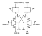
従来の広く用いられているレベルシフタを図23に示す。これは、0〜VDD1(>0、例えば5V)の電圧振幅の信号を、0〜VDD2(>VDD1、例えば10V)の電圧振幅の信号に変換する、つまり低電位側は固定で高電位側をシフトさせるレベルシフタである。このレベルシフタの構成は以下のようになっている。電源VDD2に、PチャネルMOSトランジスタ(以下、PMOSTと略す)101のソースおよびPMOST102のソースをそれぞれ接続し、PMOST101のドレインをPMOST103のソースへ、PMOST102のドレインをPMOST104のソースへそれぞれ接続している。また、PMOST103のドレインをPMOST102のゲートとNチャネルMOSトランジスタ(以下、NMOSTと略す)105のドレインへ接続し、PMOST104のドレインをPMOST101のゲートとNMOST106のドレインへ接続し、NMOST105のソースとNMOST106のソースをGND(0V)へ接続している。また、入力信号(IN)はPMOST103とNMOST105のゲートへ、入力信号(IN)の反転入力信号(/IN)はPMOST104とNMOST106のゲートへそれぞれ入力され、NMOST106のドレインから出力信号(OUT)を取り出している。なお、NMOST105のドレインから前記出力信号(OUT)の反転出力信号(/OUT)を取り出すこともできる。
【0007】
なお、本明細書においては電源電圧がVDD#の電源を電源VDD#と表記する。また、5種類のの電源電圧としてGND、VDD1、VDD2、VDD3、VDD4を取り扱うが、これらの大小関係は、
VDD4<VDD3<GND<VDD1<VDD2
を満たすものとする。ただし、説明を容易にするためGNDは0Vとした。
【0008】
次に、この従来例のレベルシフタの基本的な動作を説明する。入力信号(IN)の電位がVDD1の“Hi”の時、NMOST105はオンしPMOST103はオフするので、PMOST102のゲートは電位がGNDの“Lo”が入力されPMOST102はオンする。一方、反転入力信号(/IN)は電位がGNDの“Lo”なので、NMOST106はオフしPMOST104はオンする。従って、PMOST102、104が共にオンしたことになり出力(OUT)は、電位がシフトしてVDD2の“Hi”の状態となる。なお、PMOST101はオフになりPMOST102のゲートを電位がGNDの“Lo”レベルに保持することを保証する。
【0009】
入力信号(IN)の電位がGNDの“Lo”の時は、図23に示すレベルシフタが対称構造をとることから上記と同様に理解でき、出力端子(OUT)からは電位がGND(0V)の“Lo”が出力される。
【0010】
このようにして、0〜VDD1の電圧振幅の信号は、0〜VDD2の電圧振幅の信号に変換される。
【0011】
次に、高電位側は固定で低電位側をシフトさせる従来例のレベルシフタを図24に示す。これは、VDD3(<0)〜0の電圧振幅の信号を、VDD4(<VDD3)〜0の電圧振幅の信号に変換するものである。このレベルシフタの構成は以下のようになっている。電源VDD4に、NMOST107のソースおよびNMOST108のソースをそれぞれ接続し、NMOST107のドレインをNMOST109のソースへ、NMOST108のドレインをNMOST110のソースへそれぞれ接続している。また、NMOST109のドレインをNMOST108のゲートとPMOST111のドレインへ接続し、NMOST110のドレインをNMOST107のゲートとPMOST112のドレインへ接続し、PMOST111のソースとPMOST112のソースをそれぞれGND(0V)へ接続している。また、入力信号(IN)はNMOST109とPMOST111のゲートへ、入力信号(IN)の反転入力信号(/IN)はNMOST110とPMOST112のゲートへそれぞれ入力され、PMOST112のドレインから出力信号(OUT)を取り出している。なお、PMOST111のドレインから前記出力信号(OUT)の反転出力信号(/OUT)を取り出すこともできる。
【0012】
次に、図24で示される従来例のレベルシフタの基本的な動作を説明する。入力信号(IN)の電位がVDD3の“Lo”の時、PMOST111はオンしNMOST109はオフするので、NMOST108のゲートは電位がGNDの“Hi”が入力されNMOST108はオンする。一方、反転入力信号(/IN)は電位がGNDの“Hi”なので、PMOST112はオフしNMOST110はオンする。従って、NMOST108、110が共にオンしたことになり出力(OUT)は電位がシフトしてVDD4の“Lo”の状態となる。なお、NMOST107はオフになりNMOST108のゲートを電位がGNDの“Hi”レベルに保持することを保証する。
【0013】
入力信号(IN)の電位がGNDの“Hi”の時は、図24に示すレベルシフタが対称構造をとることから上記と同様に理解でき、出力端子(OUT)からは電位がGNDの“Hi”が出力される。
【0014】
このようにして、VDD3〜0の電圧振幅の信号は、VDD4〜0の電圧振幅の信号に変換される。
【0015】
【発明が解決しようとする課題】
上記で説明した従来例のレベルシフタは、小さな電圧振幅差間のレベル変換は比較的容易に行えるが、その電圧振幅差間が大きくなればなる程レベル変換は困難になり、問題点も生じてくる。以下に、これらの問題点について説明する。
【0016】
従来例のレベルシフタの基本的な動作は上記で簡単に説明したが、正確には変換する電圧振幅やトランジスタの特性などに依存して動作の可否や動作時間などが決まってくる。図23に示したレベルシフタにおいて、例えば、VDD1=5V、VDD2=15V、PMOST101〜104のしきい値電圧=−2V、NMOST105および106のしきい値電圧=2Vとする。この条件で、且つ正常動作時における定常状態の下で、入力信号(IN)が、電位が0Vの“Lo”から電位が5Vの“Hi”に変化すると、NMOST105はそのゲート・ソース間電圧がNMOST105のしきい値電圧を超えるのでNMOST105はオンする。一方、PMOST103のソース電位は初め15Vであるので、そのゲート・ソース間電圧は−10VでありPMOST103のしきい値電圧を超え、これもオンの状態となる。PMOST101も初めはオン状態であるので、電源VDD2とGND間にPMOST101、103、NMOST105を介して貫通電流が流れることになる。この状態は、PMOST101或いはPMOST103がオフにならない限り継続する。従ってこの貫通電流を回避するために、まず、1)PMOST101をオフにする方法、次ぎに、2)PMOST103をオフにする方法、を考える。
【0017】
1)PMOST101をオフにする方法
PMOST101をオフにするには、PMOST102および104をオンしてPMOST102のソースに接続された電源VDD2から電荷の供給を受けてPMOST101のゲート電位を13V以上にする必要がある。ここで、入力信号(IN)の反転入力信号(/IN)は、電位が0Vの“Lo”なので、NMOST106はオフ、PMOST104はオンになる。PMOST102がオンになればNMOST106がオフなので貫通電流が流れることなく速やかにPMOST101のゲート電位を15Vまで充電できるが、そのためにはPMOST102のゲート電位が13Vより小さくなる、すなわちPMOST102のゲートからNMOST105を介してGNDへ電荷を放電する必要がある。しかし、前述したようにPMOST101、103、NMOST105を介して貫通電流が流れているのでPMOST102のゲートからの放電は十分ではない。結局、貫通電流が流れた状態でNMOST105のドレイン電位が13Vより小さくなるようにPMOST101、103およびNMOST105の設計をすればPMOST101をオフにすることができる。
【0018】
2)PMOST103をオフにする方法
PMOST103をオフにするにはそのゲート・ソース間電圧を−2V以上にする必要がある。入力信号(IN)が5Vなので、PMOST103のゲート電位も同じく5Vである。したがって、PMOST103のソース電位を7V以下にする必要がある。この場合も、貫通電流が流れた状態でNMOST103のソース電位が7Vより小さくなるようにPMOST101、103およびNMOST105の設計をすればPMOST103をオフにすることができる。
【0019】
いずれにしても上述した2つの方法は、貫通電流が流れてもそれをカットしレベル変換ができるようにオン抵抗などを考慮してPMOST101、103、NMOST105を設計しなくてはならない。また、高速に動作させるには、PMOST101のソースに接続された電源VDD2からPMOST101、103を介してPMOST102のゲートへ流れ込む電流を如何に抑え、NMOST105を介してPMOST102のゲートからGNDへ流出する電流を如何に増やすかに関わってくる。また、PMOST102がオンしてから出力(OUT)を速く“Hi”に立ち上がらせるにはPMOST102、104の電流駆動能力も考慮されなければならない。
【0020】
入力信号(IN)が、電位が5Vの“Hi”から電位が0Vの“Lo”に変化する時は、PMOST101と102、PMOST103と104、NMOST105と106、それぞれの役割が入れ替わるだけなので上記で述べたことも各トランジスタを入れ替えればそのまま通用する。
【0021】
以上により、図23の従来例のレベルシフタについては、PMOST101〜104は最低限の電流駆動能力を持ち、NMOST105、106はPMOST101〜104と較べて大きな電流駆動能力を持つように設計することがポイントとなる。これに従えば、電圧振幅差間の大きなレベル変換になればなる程、NMOST105や106はチャネル幅を長く設計すれば良いが、レベルシフタ自体が大きくなり、また、入力ゲート容量も大きくなることから上流の回路もそれにつれて大きくなり、回路の占有面積の増大を招く。
【0022】
同様なことは、図24の従来例のレベルシフタについてもいえる。
【0023】
そこで、本発明は、動作の過渡期に生じる貫通電流に起因する消費電力を減少させ、大きな電圧振幅差間のレベル変換を容易にし、且つ、動作速度を向上させつつ回路の占有面積の増加を抑制するレベルシフタを新たに提供するものである。
【0024】
【課題を解決するための手段】
本発明のある一態様によるレベルシフタは、第1の電源に接続されたソースと、第1の入力信号が入力されたゲートとを有する第1導電型式の第1のMOSトランジスタと、前記第1の電源に接続されたソースと、前記第1の入力信号の反転信号である第2の入力信号が入力されたゲートとを有する、前記第1導電形式と同じ導電形式の第2のMOSトランジスタと、を有する。
【0025】
さらに、前記第1のMOSトランジスタのドレインに接続されたドレインと、前記第1の入力信号が入力されたゲートとを有する、前記第1導電形式とは別の導電形式である第2導電形式の第3のMOSトランジスタと、前記第2のMOSトランジスタのドレインに接続されたドレインと、前記第2の入力信号が入力されたゲートとを有する、前記第2導電形式と同じ導電形式の第4のMOSトランジスタと、を有する。
【0026】
さらに、前記第3のMOSトランジスタのソースに接続されたドレインと、前記第2のMOSトランジスタのドレインに接続されたゲートとを有する、前記第2導電形式と同じ導電形式の第5のMOSトランジスタと、前記第4のMOSトランジスタのソースに接続されたドレインと、前記第1のMOSトランジスタのドレインに接続されたゲートとを有する、前記第2導電形式と同じ導電形式の第6のMOSトランジスタと、を有する。
【0027】
さらに、前記第5のMOSトランジスタのソースおよび第2の電源との間に接続された第1の電圧調整回路と、前記第6のMOSトランジスタのソースおよび前記第2の電源との間に接続された第2の電圧調整回路と、を有する。
【0028】
このレベルシフタは、第1の電圧振幅の前記第1および第2の入力信号を、第2の電圧振幅の信号に変換して前記第1のMOSトランジスタのドレインと前記第2のMOSトランジスタのドレインの少なくとも一方から出力する。前記2つの電圧調整回路は、レベル変換動作の過渡期における前記第5のMOSトランジスタのソース電位および前記第6のMOSトランジスタのソース電位を調整することで、大きな電圧振幅差間のレベル変換を容易にし上記の課題を解決する。
【0029】
本発明の別のある一態様によるレベルシフタは、第1の電源に接続されたソースと、第1の入力信号が入力されたゲートとを有する第1導電型式の第1のMOSトランジスタと、前記第1の電源に接続されたソースと、前記第1の入力信号の反転信号である第2の入力信号が入力されたゲートとを有する、前記第1導電形式と同じ導電形式の第2のMOSトランジスタと、を有する。
【0030】
さらに、前記第1のMOSトランジスタのドレインに接続されたドレインと、前記第2のMOSトランジスタのドレインに接続されたゲートとを有する、前記第1導電形式とは別の導電形式である第2導電形式の第3のMOSトランジスタと、前記第2のMOSトランジスタのドレインに接続されたドレインと、前記第1のMOSトランジスタのドレインに接続されたゲートとを有する、前記第2導電形式と同じ導電形式の第4のMOSトランジスタと、を有する。
【0031】
さらに、前記第3のMOSトランジスタのソースおよび第2の電源との間に接続された第1の電圧調整回路と、前記第4のMOSトランジスタのソースおよび前記第2の電源との間に接続された第2の電圧調整回路と、を有する。
【0032】
このレベルシフタは、第1の電圧振幅の前記第1および第2の入力信号を、第2の電圧振幅の信号に変換して前記第1のMOSトランジスタのドレインと前記第2のMOSトランジスタのドレインの少なくとも一方から出力する。前記2つの電圧調整回路は、レベル変換動作の過渡期における前記第3のMOSトランジスタのソース電位および前記第4のMOSトランジスタのソース電位を調整することで、大きな電圧振幅差間のレベル変換を容易にし上記の課題を解決する。
【0033】
上記電圧調整回路は、ドレインとゲートが接続されたMOSトランジスタを有するものでもよい。
【0034】
また、上記電圧調整回路は、不純物を添加されたシリコン層またはポリシリコン層を含む抵抗器を有するものでもよい。
【0035】
また、上記電圧調整回路は、ゲートに定電圧を印加されたMOSトランジスタを有するものでもよい。
【0036】
【発明の実施の形態】
以下、本発明の実施の形態について,図面を参照しながら説明する。なお、従来例との比較を容易にするため、以下の実施形態の説明には従来例の各部に対応するトランジスタなどについては同一の符号を用いた。
【0037】
[実施形態1]
本実施形態では、信号の低電位側は固定で高電位側をシフトさせる図1に示す形態のレベルシフタについて説明する。その構成は、まず電源VDD2(>VDD1>0)に、電流が流れることで電位差を発生させる素子或いは回路(以下、電圧調整回路と言う)を2つ(10a、10b)接続する。電圧調整回路10は少なくとも2つの端子を有し、その第1の端子は電源VDD2に接続し第2の端子はPMOSTのソースに接続する。図1においては、第1の電圧調整回路10aの第2の端子はPMOST101のソースに、そして第2の電圧調整回路10bの第2の端子はPMOST102のソースにそれぞれ接続する。PMOST101のドレインはPMOST103のソースへ、PMOST102のドレインはPMOST104のソースへそれぞれ接続する。また、PMOST103のドレインはPMOST102のゲートおよびNMOST105のドレインへ接続し、PMOST104のドレインはPMOST101のゲートおよびNMOST106のドレインへ接続する。NMOST105のソースおよびNMOST106のソースはGND(0V)へ接続する。また、0〜VDD1の電圧振幅である入力信号(IN)はPMOST103およびNMOST105のゲートへ、同じ電圧振幅である、入力信号(IN)の反転入力信号(/IN)は、PMOST104およびNMOST106のゲートへそれぞれ入力され、NMOST106のドレインからレベル変換された出力信号(OUT)を取り出している。なお、NMOST105のドレインから前記出力信号(OUT)の反転出力信号(/OUT)を取り出すこともできる。2つの電圧調整回路10aおよび10bが電源VDD2とPMOST101および102のソースとの間に接続されていることが従来例と異なる。
【0038】
これらの電圧調整回路10aおよび10bにより、レベル変換動作の過渡期に生じる貫通電流が流れる時に、PMOST101および102のソース電位を電源電圧VDD2より小さくし、大きな電圧振幅差間のレベル変換動作を容易にさせる。容易にレベル変換できればレベル変換動作も高速になり、これは貫通電流が流れる時間の減少、つまり消費電力の低減にも効果がある。
【0039】
[実施形態2]
本実施形態では、信号の高電位側は固定で低電位側をシフトさせる図2に示す形態のレベルシフタについて説明する。その構成は、まず電源VDD4(<VDD3<0)に、実施形態1と同様に2つの電圧調整回路10cおよび10dの第1の端子を接続する。第1の電圧調整回路10cの第2の端子はNMOST107のソースに、そして第2の電圧調整回路10dの第2の端子はNMOST108のソースにそれぞれ接続する。NMOST107のドレインはNMOST109のソースへ、NMOST108のドレインはNMOST110のソースへそれぞれ接続する。また、NMOST109のドレインはNMOST108のゲートおよびPMOST111のドレインへ接続し、NMOST110のドレインはNMOST107のゲートおよびPMOST112のドレインへ接続する。PMOST111のソースおよびPMOST112のソースはGND(0V)へ接続する。また、VDD3〜0の電圧振幅である入力信号(IN)はNMOST109およびPMOST111のゲートへ、同じ電圧振幅である、入力信号(IN)の反転入力信号(/IN)は、NMOST110およびPMOST112のゲートへそれぞれ入力され、PMOST112のドレインからレベル変換された出力信号(OUT)を取り出している。なお、PMOST111のドレインから前記出力信号(OUT)の反転出力信号(/OUT)を取り出すこともできる。2つの電圧調整回路10cおよび10dが電源VDD4とNMOST107および108のソースとの間に接続されていることが従来例と異なる。
【0040】
これらの電圧調整回路10cおよび10dにより、レベル変換動作の過渡期に生じる貫通電流が流れる時に、NMOST107および108のソース電位を電源電圧VDD4より大きくし、大きな電圧振幅差間のレベル変換動作を容易にさせる。容易にレベル変換できればレベル変換動作も高速になり、これは貫通電流が流れる時間の減少、つまり消費電力の低減にも効果がある。
【0041】
[実施形態3]
本実施形態では、信号の低電位側は固定で高電位側をシフトさせる実施形態1とは異なる図3に示す形態のレベルシフタについて説明する。その構成は、まず電源VDD2(>VDD1>0)に、実施形態1と同様に2つの電圧調整回路10aおよび10bの第1の端子を接続する。第1の電圧調整回路10aの第2の端子はPMOST101のソースに、そして第2の電圧調整回路10bの第2の端子はPMOST102のソースにそれぞれ接続する。PMOST101のドレインはPMOST102のゲートおよびNMOST105のドレインへ接続し、PMOST102のドレインはPMOST101のゲートおよびNMOST106のドレインへ接続する。NMOST105のソースおよびNMOST106のソースはGND(0V)へ接続する。また、0〜VDD1の電圧振幅である入力信号(IN)はNMOST105のゲートへ、同じ電圧振幅である、入力信号(IN)の反転入力信号(/IN)は、NMOST106のゲートへそれぞれ入力され、NMOST106のドレインからレベル変換された出力信号(OUT)を取り出している。なお、NMOST105のドレインから前記出力信号(OUT)の反転出力信号(/OUT)を取り出すこともできる。実施形態1におけるPMOST103および104が削除されたものが本実施形態である。なお、比較を容易にするため、実施形態1と対応する部分には同一の符号を用いた。
【0042】
これらの電圧調整回路10aおよび10bにより、レベル変換動作の過渡期に生じる貫通電流が流れる時に、PMOST101および102のソース電位を電源電圧VDD2より小さくし、大きな電圧振幅差間のレベル変換動作を容易にさせる。容易にレベル変換できればレベル変換動作も高速になり、これは貫通電流が流れる時間の減少、つまり消費電力の低減にも効果がある。また、実施形態1と比べてトランジスタ数を削減することが可能である。
【0043】
[実施形態4]
本実施形態では、信号の高電位側は固定で低電位側をシフトさせる実施形態2とは異なる図4に示す形態のレベルシフタについて説明する。その構成は、まず電源VDD4(<VDD3<0)に、実施形態2と同様に2つの電圧調整回路10cおよび10dの第1の端子を接続する。第1の電圧調整回路10cの第2の端子はNMOST107のソースに、そして第2の電圧調整回路10dの第2の端子はNMOST108のソースにそれぞれ接続する。NMOST107のドレインはNMOST108のゲートおよびPMOST111のドレインへ接続し、NMOST108のドレインはNMOST107のゲートおよびPMOST112のドレインへ接続する。PMOST111のソースおよびPMOST112のソースはGND(0V)へ接続する。また、VDD3〜0の電圧振幅である入力信号(IN)はPMOST111のゲートへ、同じ電圧振幅である、入力信号(IN)の反転入力信号(/IN)はPMOST112のゲートへそれぞれ入力され、PMOST112のドレインからレベル変換された出力信号(OUT)を取り出している。なお、PMOST111のドレインから前記出力信号(OUT)の反転出力信号(/OUT)を取り出すこともできる。実施形態2におけるNMOST109および110が削除されたものが本実施形態である。なお、比較を容易にするため、実施形態2と対応する部分には同一の符号を用いた。
【0044】
これらの電圧調整回路10cおよび10dにより、レベル変換動作の過渡期に生じる貫通電流が流れる時に、NMOST107および108のソース電位を電源電圧VDD4より大きくし、大きな電圧振幅差間のレベル変換動作を容易にさせる。容易にレベル変換できればレベル変換動作も高速になり、これは貫通電流が流れる時間の減少、つまり消費電力の低減にも効果がある。また、実施形態2と比べてトランジスタ数を削減することが可能である。
【0045】
【実施例】
ここで、本発明の実施例について、図面を参照しながら説明する。
【0046】
[実施例1]
本実施例では、信号の低電位側は固定で高電位側をシフトさせる図5に示すレベルシフタについて説明する。なお、本実施例は実施形態1に対して電圧調整回路の具体例を明示した実施例である。また、本実施例は図23で示した従来例の改良型と言え、各部に対応するトランジスタなどには同一の符号を用いた。
【0047】
本実施例のレベルシフタの構成は以下のようになっている。電源VDD2に、PMOST113のソースおよびPMOST114のソースをそれぞれ接続し、PMOST113のゲートおよびドレインをPMOST101のソースへ、またPMOST114のゲートおよびドレインをPMOST102のソースへそれぞれ接続する。PMOST101のドレインはPMOST103のソースへ、PMOST102のドレインはPMOST104のソースへそれぞれ接続する。また、PMOST103のドレインはPMOST102のゲートおよびNMOST105のドレインへ接続し、PMOST104のドレインはPMOST101のゲートおよびNMOST106のドレインへ接続する。NMOST105のソースおよびNMOST106のソースはGND(0V)へ接続する。また、0〜VDD1の電圧振幅である入力信号(IN)はPMOST103およびNMOST105のゲートへ、同じ電圧振幅である、入力信号(IN)の反転入力信号(/IN)は、PMOST104およびNMOST106のゲートへそれぞれ入力され、NMOST106のドレインからレベル変換された出力信号(OUT)を取り出している。なお、NMOST105のドレインから前記出力信号(OUT)の反転出力信号(/OUT)を取り出すこともできる。PMOST113および114が追加されたことが従来例と異なる。
【0048】
引き続いて、本実施例のレベルシフタの動作について説明する。ただし、トランジスタ101〜106については従来例と同様な役割をするのでその説明は簡略化し、PMOST113および114が加わったことで動作が如何に変わるかについて主に説明する。
【0049】
図5に示したレベルシフタにおいて、例えば、VDD1=5V、VDD2=15V、PMOST101〜104および113、114のしきい値電圧=−2V、NMOST105および106のしきい値電圧=2Vとする。この条件で、入力信号(IN)の電位が0Vの“Lo”である定常状態をまず考える。この時、PMOST101および103はオンしNMOST105はオフしているのでPMOST102のゲートへは電源VDD2から充電される。ただし、PMOST113は常に飽和領域での動作となるので、充電が完了した定常状態ではPMOST101のソース電位はVDD2の電位15VからPMOST113のしきい値電圧の絶対値だけ引かれた13Vとなる。従って、PMOST102のゲート(反転出力信号(/OUT))もその電位が13Vの“Hi”となる。一方、PMOST102はオフ、NMOST106はオンなのでPMOST101のゲート(出力信号(OUT))は電位が0Vの“Lo”であり、PMOST102のソース電位はPMOST101のそれと同様に13Vとなる。
【0050】
この状態から入力信号(IN)が、電位が5Vの“Hi”になるとどうなるかを次に考える。この時も、入力信号の変化の直後は前述と同様にPMOST101、103およびNMOST105はオンなので、PMOST113のソースに接続された電源VDD2とNMOST105のソースに接続されたGNDとの間を貫通電流が流れようとする。ただし、飽和領域で動作するPMOST113があるために、流れようとする電流の分だけPMOST113のソース・ドレイン間電圧が更に大きくなり(以下、この大きくなった分をΔ1とする)、PMOST101のソース電位は(13−Δ1)Vと更に小さくなる。従って、従来例のレベルシフタにおいて電源電圧VDD2を15Vから(13−Δ1)Vへと小さくしたのと同じ効果が得られる。このΔ1は、貫通電流が大きいほど大きくなりPMOST101のソース電位もそれに合わせて小さくなりPMOST101や103がオフになり易くなり、結果的に貫通電流もカットされるように働く。一方、貫通電流が小さいとNMOST105を介してPMOST102のゲートから放電される電流が勝り、直ちにPMOST102がオンになる。これによりPMOST101のゲートは13Vに充電され、結局このトランジスタのオフに結びつく。このようにPMOST113はレベル変換を容易にする効果を持つ。
【0051】
これらの様子は、図6に示すシミュレーション結果により確認できる。図中には同時に従来例の結果も白抜きのマークにより示した。なお、シミュレーションに用いたトランジスタの主なパラメータは、全てのPMOSTのしきい値電圧、移動度をそれぞれ−2V、100cm2/Vsとし、全てのNMOSTのしきい値電圧、移動度をそれぞれ2V、100cm2/Vsとした。また、トランジスタのチャネル長は全て4μmとし、チャネル幅については、PMOST101〜104は10μm、NMOST105、106は30μm、PMOST113、114は20μmとした。なお、Vs101はPMOST101のソース電位を、I1はPMOST1010のソース・ドレイン間を流れる電流をそれぞれ示す。従来例に比べてレベル変換の動作速度が向上し、貫通電流も少なく低消費電力であることが分かる。
【0052】
また、NMOST105、106のチャネル幅(W)を変え(他の条件は前述と同じ)、入力信号(IN)が50%立ち上がってから、出力信号(OUT)が7.5V(15Vの50%とした)に立ち上がるまでの遅延時間(Td)をシミュレーションにより求めたものを図7(A)に示す。従来例に比べ、NMOST105および106のチャネル幅が約20μm小さくても同等の動作をすることが示されている。従って、PMOST113および114を付加したことによる回路の占有面積増加は殆どない。
【0053】
図7(B)には、電源電圧VDD2を変えたときの遅延時間(Td)をシミュレーションした結果である。ただし、この場合の遅延時間は入力信号(IN)が50%立ち上がってから、出力信号(OUT)が電源電圧VDD2の50%立ち上がるまでの時間とした。また、この時のシミュレーションに用いた移動度、しきい値などは前述と同じで、チャネル幅については、PMOST101〜104は10μm、NMOST105、106は20μm、PMOST113、114は10μmとした。比較のため図7(B)には従来例のシミュレーション結果も示した。ただし、従来例についてはNMOST105、106のチャネル幅を30μmとして、本実施例で付加したPMOST113、114の分だけ大きくし占有面積がほぼ同じ条件とした。図から判るように従来例では大きな電圧振幅差間のレベル変換が困難であるのに対し、本実施例では容易にレベル変換が可能である。また、従来例では電源電圧VDD2を増加させると急激にレベル変換が破綻する傾向にあるが、本発明ではそれが緩やかなため、トランジスタの特性バラツキにも強いレベルシフタであると言える。
【0054】
入力信号(IN)が、電位が5Vの“Hi”から電位が0Vの“Lo”に変化するときは、PMOST113と114、PMOST101と102、PMOST103と104、NMOST105と106、それぞれの役割が入れ替わるだけなので上記で述べたことも各トランジスタを入れ替えればそのまま通用する。
【0055】
[実施例2]
本実施例でも、信号の低電位側は固定で高電位側をシフトさせるレベルシフタの別例について説明する。本実施例のレベルシフタは図8で示されるように、実施例1のレベルシフタにおいてPMOST113、114をNMOST115、116にそれぞれ置き換え、それらのゲートを電源VDD2と接続したものである。なお、本実施例も実施形態1に対して電圧調整回路の具体例を明示した実施例である。また、本実施例も図23で示した従来例の改良型と言え、各部に対応するトランジスタなどには同一の符号を用いた。
【0056】
本実施例のレベルシフタの構成は以下のようになっている。電源VDD2に、NMOST115のドレインおよびゲートを、そしてNMOST116のドレインおよびゲートをそれぞれ接続し、NMOST115のソースをPMOST101のソースへ、またNMOST116のソースをPMOST102のソースへそれぞれ接続する。PMOST101のドレインはPMOST103のソースへ、PMOST102のドレインはPMOST104のソースへそれぞれ接続する。また、PMOST103のドレインはPMOST102のゲートおよびNMOST105のドレインへ接続し、PMOST104のドレインはPMOST101のゲートおよびNMOST106のドレインへ接続する。NMOST105のソースおよびNMOST106のソースはGND(0V)へ接続する。また、0〜VDD1の電圧振幅である入力信号(IN)はPMOST103およびNMOST105のゲートへ、同じ電圧振幅である、入力信号(IN)の反転入力信号(/IN)は、PMOST104およびNMOST106のゲートへそれぞれ入力され、NMOST106のドレインからレベル変換された出力信号(OUT)を取り出している。なお、NMOST105のドレインから前記出力信号(OUT)の反転出力信号(/OUT)を取り出すこともできる。NMOST115および116が追加されたことが従来例と異なる。
【0057】
本実施例のレベルシフタは、その動作については基本的には実施例1と同じであり、実施例1におけるPMOST113および114の役割をNMOST115および116に代替させたものである。従って、本実施例のレベルシフタは、0〜VDD1の電圧振幅の信号を、0〜(VDD2−Vth1)の電圧振幅の信号に変換する。ここで、Vth1はNMOST115または116のしきい値電圧である。
【0058】
以上のように、本実施例のレベルシフタは実施例1と同様に、従来例に比べて大きなレベル差間のレベル変換を容易にし、動作速度も向上し、また、貫通電流も少なく消費電力の低減に効果がある。加えて、トランジスタの特性バラツキにも強い。また、本実施例では、NMOSのしきい値電圧をPMOSTのしきい値電圧の絶対値より小さくするようにトランジスタを作成すれば、本実施例のレベルシフタの出力信号を入力する次段の論理回路のPMOSTをオフするマージンを十分持たせることができる。
【0059】
[実施例3]
本実施例では、信号の高電位側は固定で低電位側をシフトさせる図9に示すレベルシフタについて説明する。なお、本実施例は実施形態2に対して電圧調整回路の具体例を明示した実施例である。また、本実施例は図24で示した従来例の改良型と言え、各部に対応するトランジスタなどには同一の符号を用いた。
【0060】
本実施例のレベルシフタの構成は以下のようになっている。電源VDD4に、NMOST117のソースおよびNMOST118のソースをそれぞれ接続し、NMOST117のゲートおよびドレインをNMOST107のソースへ、また、NMOST118のゲートおよびドレインをNMOST108のソースへそれぞれ接続する。NMOST107のドレインはNMOST109のソースへ、NMOST108のドレインはNMOST110のソースへそれぞれ接続する。また、NMOST109のドレインはNMOST108のゲートおよびPMOST111のドレインへ接続し、NMOST110のドレインはNMOST107のゲートおよびPMOST112のドレインへ接続し、PMOST111のソースおよびPMOST112のソースをそれぞれGND(0V)へ接続する。また、VDD3〜0の電圧振幅である入力信号(IN)はNMOST109およびPMOST111のゲートへ、同じ電圧振幅である、入力信号(IN)の反転入力信号(/IN)はNMOST110およびPMOST112のゲートへそれぞれ入力し、PMOST112のドレインからレベル変換された出力信号(OUT)を取り出している。なお、PMOST111のドレインから前記出力信号(OUT)の反転出力信号を取り出すこともできる。NMOST117およびNMOST118が追加されたことが従来例と異なる。
【0061】
引き続いて、本実施例のレベルシフタの動作について説明する。ただし、トランジスタ107〜112については従来例と同様な役割をするのでその説明は簡略化し、NMOST117および118が加わったことで動作が如何に変わるかについて主に説明する。
【0062】
図9に示したレベルシフタにおいて、例えば、VDD3=−5V、VDD4=−15V、NMOST107〜110および117、118のしきい値電圧=2V、PMOST111および112のしきい値電圧=−2Vとする。この条件で、入力信号(IN)の電位が0Vの“Hi”である定常状態をまず考える。この時、NMOST107および109はオンしPMOST111はオフしているのでNMOST108のゲートに蓄えられた電荷は電源VDD4へ放電される。ただし、NMOST117は常に飽和領域での動作となるので、放電が完了した定常状態ではNMOST107のソースの電位は電源電圧VDD4の電位−15VからNMOST117のしきい値電圧だけ足された−13Vとなる。従って、NMOST108のゲート(反転出力信号(/OUT))もその電位が−13Vの“Lo”となる。一方、NMOST108はオフ、PMOST112はオンなのでNMOST107のゲート(出力信号(OUT))は電位が0Vの“Hi”であり、NMOST108のソースはNMOST117のそれと同様に−13Vとなる。
【0063】
この状態から入力信号(IN)が、電位が−5Vの“Lo”になるとどうなるかを次に考える。この時も、入力信号の変化の直後は前述と同様にNMOST107、109およびPMOST111はオンなので、NMOST117のソースに接続された電源VDD4とPMOST111のソースに接続されたGNDとの間を貫通電流が流れようとする。ただし、飽和領域で動作するNMOST117があるために、流れようとする電流の分だけNMOST117のソース・ドレイン間電圧が更に大きくなり(以下、この大きくなった分をΔ2とする)、NMOST107のソース電位は−(13−Δ2)Vと更に大きくなる。従って、従来例のレベルシフタにおいて電源電圧VDD4を−15Vから−(13−Δ2)Vへと大きくしたのと同じ効果が得られる。このΔ2は、貫通電流が大きいほど大きくなりNMOST107のソース電位もそれに合わせて大きくなりNMOST107や109がオフになり易くなり、結果的に貫通電流もカットされるように働く。一方、貫通電流が小さいとPMOST111を介してNMOST108のゲートへ充電される電流が勝り、直ちにNMOST108がオンになる。これによりNMOST107のゲートは−13Vに充電され、結局このトランジスタのオフに結びつく。このようにNMOST117はレベル変換を容易にする効果を持つ。
【0064】
これらの様子は、図10に示すシミュレーション結果により確認できる。図中には同時に従来例の結果も白抜きのマークにより示した。なお、シミュレーションに用いたトランジスタの主なパラメータは、全てのPMOSTのしきい値電圧、移動度をそれぞれ−2V、100cm2/Vsとし、全てのNMOSTのしきい値電圧、移動度をそれぞれ2V、100cm2/Vsとした。また、トランジスタのチャネル長は全て4μmとし、チャネル幅については、NMOST107〜110は10μm、PMOST111、112は30μm、NMOST117、118は20μmとした。なお、Vs107はNMOST107のソース電位を、I2はNMOST1070のソース・ドレイン間を流れる電流をそれぞれ示す。従来例に比べてレベル変換の動作速度が向上し、貫通電流も少なく低消費電力であることが分かる。また、実施例1と同様に本実施例のレベルシフタはトランジスタの特性バラツキにも強い。
【0065】
入力信号(IN)が、電位が−5Vの“Lo”から電位が0Vの“Hi”に変化するときは、NMOST117と118、NMOST107と108、NMOST109と110、PMOST111と112、それぞれの役割が入れ替わるだけなので上記で述べたことも各トランジスタを入れ替えればそのまま通用する。
【0066】
[実施例4]
本実施例でも、信号の高電位側は固定で低電位側をシフトさせるレベルシフタの別例について説明する。本実施例のレベルシフタは図11で示されるように、実施例3のレベルシフタにおいてNMOST117、118をPMOST119、120にそれぞれ置き換え、それらのゲートを電源VDD4と接続したものである。なお、本実施例も実施形態2に対して電圧調整回路の具体例を明示した実施例である。また、本実施例も図24で示した従来例の改良型と言え、各部に対応するトランジスタなどには同一の符号を用いた。
【0067】
本実施例のレベルシフタの構成は以下のようになっている。電源VDD4に、PMOST119のドレインおよびゲートを、PMOST120のドレインおよびゲートをそれぞれ接続し、PMOST119のソースをNMOST107のソースへ、また、PMOST120のソースをNMOST108のソースへそれぞれ接続する。NMOST107のドレインはNMOST109のソースへ、NMOST108のドレインはNMOST110のソースへそれぞれ接続する。また、NMOST109のドレインはNMOST108のゲートおよびPMOST111のドレインへ接続し、NMOST110のドレインはNMOST107のゲートおよびPMOST112のドレインへ接続し、PMOST111のソースおよびPMOST112のソースはそれぞれGND(0V)へ接続する。また、VDD3〜0の電圧振幅である入力信号(IN)はNMOST109およびPMOST111のゲートへ、同じ電圧振幅である、入力信号(IN)の反転入力信号(/IN)はNMOST110およびPMOST112のゲートへそれぞれ入力し、PMOST112のドレインからレベル変換された出力信号(OUT)を取り出している。なお、PMOST111のドレインから前記出力信号(OUT)の反転出力信号を取り出すこともできる。PMOST119およびPMOST120が追加されたことが従来例と異なる。
【0068】
本実施例のレベルシフタは、その動作については基本的には実施例3と同じであり、実施例3におけるNMOST117および118の役割をPMOST119および120に代替させたものである。従って、本実施例のレベルシフタは、VDD3〜0の電圧振幅の信号を、(VDD4−Vth2)〜0の電圧振幅の信号に変換する。ここで、Vth2はNMOST119または120のしきい値電圧である。
【0069】
以上のように、本実施例のレベルシフタは実施例3と同様に、従来例に比べて大きなレベル差間のレベル変換を容易にし、動作速度も向上し、また、貫通電流も少なく消費電力の低減に効果がある。加えて、トランジスタの特性バラツキにも強い。また、本実施例では、PMOSのしきい値電圧の絶対値をNMOSTのしきい値電圧より小さくするようにトランジスタを作成すれば、本実施例のレベルシフタの出力信号を入力する次段の論理回路のNMOSTをオフするマージンを十分持たせることができる。
【0070】
[実施例5]
本実施例では、信号の低電位側は固定で高電位側をシフトさせる図12に示すレベルシフタについて説明する。なお、本実施例は実施形態3に対して電圧調整回路の具体例を明示した実施例である。また、本実施例は、図5で示される実施例1の改良型とも言え、各部に対応するトランジスタなどには同一の符号を用いた。
【0071】
本実施例のレベルシフタの構成は以下のようになっている。電源VDD2に、PMOST113のソースおよびPMOST114のソースをそれぞれ接続し、PMOST113のゲートおよびドレインをPMOST101のソースへ、またPMOST114のゲートおよびドレインをPMOST102のソースへそれぞれ接続する。PMOST101のドレインはPMOST102のゲートおよびNMOST105のドレインへ接続し、PMOST102のドレインはPMOST101のゲートおよびNMOST106のドレインへ接続する。NMOST105のソースおよびNMOST106のソースはGND(0V)へ接続する。また、0〜VDD1の電圧振幅である入力信号(IN)はNMOST105のゲートへ、同じ電圧振幅である、入力信号(IN)の反転入力信号(/IN)はNMOST106のゲートへそれぞれ入力され、NMOST106のドレインからレベル変換された出力信号(OUT)を取り出している。なお、NMOST105のドレインから前記出力信号(OUT)の反転出力信号(/OUT)を取り出すこともできる。
【0072】
本実施例のレベルシフタは、その動作については基本的には実施例1と同じであり、実施例1におけるPMOST103および104を削除したものである。大きなレベル差間のレベル変換では、これらPMOST103および104は本来の役割を果たさないので削除しても問題にはならない。本実施例のレベルシフタは、0〜VDD1の電圧振幅の信号を、0〜(VDD2−Vth3)の電圧振幅の信号に変換する。ここで、Vth3はPMOST113または114のしきい値電圧である。
【0073】
以上のように、本実施例のレベルシフタは実施例1と同様に、従来例に比べて大きなレベル差間のレベル変換を容易にし、動作速度も向上し、また、貫通電流も少なく消費電力の低減に効果がある。加えて、トランジスタの特性バラツキにも強い。なお、本実施例は従来例と同じトランジスタの個数で構成されるので同程度の動作特性のレベルシフタであれば回路の占有面積は小さくすることができる。
【0074】
[実施例6]
本実施例でも、信号の低電位側は固定で高電位側をシフトさせるレベルシフタの別例について説明する。本実施例のレベルシフタは図13で示されるように、図12で示した実施例5のレベルシフタにおいてPMOST113、114をNMOST115、116にそれぞれ置き換え、それらのゲートを電源VDD2と接続したものである。なお、本実施例も実施形態3に対して電圧調整回路の具体例を明示した実施例である。また、本実施例は図8で示した実施例2の改良型とも言え、各部に対応するトランジスタなどには同一の符号を用いた。
【0075】
本実施例のレベルシフタの構成は以下のようになっている。電源VDD2に、NMOST115のドレインおよびゲートを、そしてNMOST116のドレインおよびゲートをそれぞれ接続し、NMOST115のソースをPMOST101のソースへ、またNMOST116のソースをPMOST102のソースへそれぞれ接続する。PMOST101のドレインはPMOST102のゲートおよびNMOST105のドレインへ接続し、PMOST102のドレインはPMOST101のゲートおよびNMOST106のドレインへ接続する。NMOST105のソースおよびNMOST106のソースはGND(0V)へ接続する。また、0〜VDD1の電圧振幅である入力信号(IN)はNMOST105のゲートへ、同じ電圧振幅である、入力信号(IN)の反転入力信号(/IN)はNMOST106のゲートへそれぞれ入力され、NMOST106のドレインから出力信号(OUT)を取り出している。なお、NMOST105のドレインから前記出力信号(OUT)の反転出力信号(/OUT)を取り出すこともできる。
【0076】
本実施例のレベルシフタは、その動作については基本的には実施例2と同じであり、実施例2におけるPMOST103および104を削除したものである。大きなレベル差間のレベル変換では、これらPMOST103および104は本来の役割を果たさないので削除しても問題にはならない。本実施例のレベルシフタは、0〜VDD1の電圧振幅の信号を、0〜(VDD2−Vth1)の電圧振幅の信号に変換する。ここで、Vth1はNMOST115または116のしきい値電圧である。
【0077】
以上のように、本実施例のレベルシフタは実施例2と同様に、従来例に比べて大きなレベル差間のレベル変換を容易にし、動作速度も向上し、また、貫通電流も少なく消費電力の低減に効果がある。加えて、トランジスタの特性バラツキにも強い。また、本実施例では、NMOSのしきい値電圧をPMOSTのしきい値電圧の絶対値より小さくするようにトランジスタを作成すれば、本実施例のレベルシフタの出力信号を入力する次段の論理回路のPMOSTをオフするマージンを十分持たせることができる。なお、本実施例は従来例と同じトランジスタの個数で構成されるので同程度の動作特性のレベルシフタであれば回路の占有面積は小さくすることができる。
【0078】
[実施例7]
本実施例では、信号の高電位側は固定で低電位側をシフトさせる図14に示すレベルシフタについて説明する。なお、本実施例は実施形態4に対して電圧調整回路の具体例を明示した実施例である。また、本実施例は、図9で示される実施例3の改良型と言え、各部に対応するトランジスタなどには同一の符号を用いた。
【0079】
本実施例のレベルシフタの構成は以下のようになっている。電源VDD4に、NMOST117のソースおよびNMOST118のソースをそれぞれ接続し、NMOST117のゲートおよびドレインをNMOST107のソースへ、またNMOST118のゲートおよびドレインをNMOST108のソースへそれぞれ接続する。NMOST107のドレインはNMOST108のゲートおよびPMOST111のドレインへ接続し、NMOST108のドレインはNMOST107のゲートおよびPMOST112のドレインへ接続する。PMOST111のソースおよびPMOST112のソースはGND(0V)へ接続する。また、VDD3〜0の電圧振幅である入力信号(IN)はPMOST111のゲートへ、同じ電圧振幅である、入力信号(IN)の反転入力信号(/IN)はPMOST112のゲートへそれぞれ入力され、PMOST112のドレインから出力信号(OUT)を取り出している。なお、PMOST111のドレインから前記出力信号(OUT)の反転出力信号(/OUT)を取り出すこともできる。
【0080】
本実施例のレベルシフタは、その動作については基本的には実施例3と同じであり、実施例3におけるNMOST109および110を削除したものである。大きなレベル差間のレベル変換では、これらNMOST109および110は本来の役割を果たさないので削除しても問題にはならない。本実施例のレベルシフタは、VDD3〜0の電圧振幅の信号を、(VDD4−Vth2)〜0の電圧振幅の信号に変換する。ここで、Vth2はNMOST119または120のしきい値電圧である。
【0081】
以上のように、本実施例のレベルシフタは実施例3と同様に、従来例に比べて大きなレベル差間のレベル変換を容易にし、動作速度も向上し、また、貫通電流も少なく消費電力の低減に効果がある。加えて、トランジスタの特性バラツキにも強い。なお、本実施例は従来例と同じトランジスタの個数で構成されるので同程度の動作特性のレベルシフタであれば回路の占有面積は小さくすることができる。
【0082】
[実施例8]
本実施例でも、信号の高電位側は固定で低電位側をシフトさせるレベルシフタの別例について説明する。本実施例のレベルシフタは図15で示されるように、図14で示した実施例7のレベルシフタにおいてNMOST117、118をPMOST119、120にそれぞれ置き換え、それらのゲートを電源VDD4と接続したものである。なお、本実施例は実施形態4に対して電圧調整回路の具体例を明示した実施例である。また、本実施例は図11で示した実施例4の改良型とも言え、各部に対応するトランジスタなどには同一の符号を用いた。
【0083】
本実施例のレベルシフタの構成は以下のようになっている。電源VDD4に、PMOST119のドレインおよびゲートを、そしてPMOST120のドレインおよびゲートをそれぞれ接続し、PMOST119のソースをNMOST107のソースへ、またPMOST120のソースをNMOST108のソースへそれぞれ接続する。NMOST107のドレインはNMOST108のゲートおよびPMOST111のドレインへ接続し、NMOST108のドレインはNMOST107のゲートおよびPMOST112のドレインへ接続する。PMOST111のソースおよびPMOST112のソースはGND(0V)へ接続する。また、VDD3〜0の電圧振幅である入力信号(IN)はPMOST111のゲートへ、同じ電圧振幅である、入力信号(IN)の反転入力信号(/IN)はPMOST112のゲートへそれぞれ入力され、PMOST107のドレインから出力信号(OUT)を取り出している。なお、PMOST111のドレインから前記出力信号(OUT)の反転出力信号(/OUT)を取り出すこともできる。図11で示される実施例4とはNMOST109および110の有無が異なる。
【0084】
本実施例のレベルシフタは、その動作については基本的には実施例4と同じであり、実施例4におけるNMOST109および110を削除したものである。大きなレベル差間のレベル変換では、これらNMOST109および110は本来の役割を果たさないので削除しても問題にはならない。本実施例のレベルシフタは、VDD3〜0の電圧振幅の信号を、(VDD4−Vth2)〜0の電圧振幅の信号に変換する。ここで、Vth2はNMOST119または120のしきい値電圧である。
【0085】
以上のように、本実施例のレベルシフタは実施例4と同様に、従来例に比べて大きなレベル差間のレベル変換を容易にし、動作速度も向上し、また、貫通電流も少なく消費電力の低減に効果がある。加えて、トランジスタの特性バラツキにも強い。また、本実施例では、PMOSのしきい値電圧の絶対値をNMOSTのしきい値電圧より小さくするようにトランジスタを作成すれば、本実施例のレベルシフタの出力信号を入力する次段の論理回路のNMOSTをオフするマージンを十分持たせることができる。なお、本実施例は従来例と同じトランジスタの個数で構成されるので同程度の動作特性のレベルシフタであれば回路の占有面積は小さくすることができる。
【0086】
[実施例9]
本実施例では、実施形態1乃至実施形態4において電圧調整回路として抵抗を用いたレベルシフタについて説明する。この抵抗としては、トランジスタのゲートをそのしきい値電圧以上にバイアスし常にオン状態にしてそのソース・ドレイン間を抵抗に利用する方法、トランジスタのソース・ドレイン領域を利用する方法、また、LDD領域を利用する方法などがある。これらの抵抗を用いることでもレベル変換動作を容易にする効果がある。なお、この場合はレベルシフタの出力振幅は、実施例1乃至実施例9のようにしきい値電圧だけ変動することはなくフルスケールとなる。
[実施例10]
本実施例では、実施例1〜実施例9のレベルシフタをアクティブマトリクス型液晶表示装置の駆動回路に適用した場合の作成方法例について説明する。なお、画素部のスイッチング素子である画素TFTと、画素部の周辺に設けられる本発明のレベルシフタを有する駆動回路(信号線駆動回路、走査線駆動回路等)のTFTとを同一基板上に作製する工程を取り上げる。但し、説明を容易にするために、駆動回路部にはその基本構成回路であるCMOS回路を、画素部の画素TFTにはnチャネル型TFTとを、ある経路に沿った断面により図示することにする。
【0087】
まず、図16(A)に示すように、コーニング社の#7059ガラスや#1737ガラスなどに代表されるバリウムホウケイ酸ガラス、またはアルミノホウケイ酸ガラスなどのガラスから成る基板400上に酸化シリコン膜、窒化シリコン膜または酸化窒化シリコン膜などの絶縁膜から成る下地膜401を形成する。例えば、プラズマCVD法でSiH4、NH3、N2Oから作製される酸化窒化シリコン膜401aを10〜200nm(好ましくは50〜100nm)形成し、同様にSiH4、N2Oから作製される酸化窒化水素化シリコン膜401bを50〜200nm(好ましくは100〜150nm)の厚さに積層形成する。本実施例では下地膜401を2層構造として示したが、前記絶縁膜の単層膜または2層以上積層させた構造として形成しても良い。
【0088】
島状半導体層402〜406は、非晶質構造を有する半導体膜をレーザー結晶化法や公知の熱結晶化法を用いて作製した結晶質半導体膜で形成する。この島状半導体層402〜406の厚さは25〜80nm(好ましくは30〜60nm)の厚さで形成する。結晶質半導体膜の材料に限定はないが、好ましくはシリコンまたはシリコンゲルマニウム(SiGe)合金などで形成すると良い。
【0089】
レーザー結晶化法で結晶質半導体膜を作製するには、パルス発振型または連続発光型のエキシマレーザーやYAGレーザー、YVO4レーザーを用いる。これらのレーザーを用いる場合には、レーザー発振器から放射されたレーザー光を光学系で線状に集光し半導体膜に照射する方法を用いると良い。結晶化の条件は実施者が適宣選択するものであるが、エキシマレーザーを用いる場合はパルス発振周波数30Hzとし、レーザーエネルギー密度を100〜400mJ/cm2(代表的には200〜300mJ/cm2)とする。また、YAGレーザーを用いる場合にはその第2高調波を用いパルス発振周波数1〜10kHzとし、レーザーエネルギー密度を300〜600mJ/cm2(代表的には350〜500mJ/cm2)とすると良い。そして幅100〜1000μm、例えば400μmで線状に集光したレーザー光を基板全面に渡って照射し、この時の線状レーザー光の重ね合わせ率(オーバーラップ率)を80〜98%として行う。
【0090】
次いで、島状半導体層402〜406を覆うゲート絶縁膜407を形成する。ゲート絶縁膜407はプラズマCVD法またはスパッタ法を用い、厚さを40〜150nmとしてシリコンを含む絶縁膜で形成する。本実施例では、120nmの厚さの酸化窒化シリコン膜で形成する。勿論、ゲート絶縁膜はこのような酸化窒化シリコン膜に限定されるものでなく、他のシリコンを含む絶縁膜を単層または積層構造として用いても良い。例えば、酸化シリコン膜を用いる場合には、プラズマCVD法でTEOS(Tetraethyl Orthosilicate)とO2とを混合し、反応圧力40Pa、基板温度300〜400℃とし、高周波(13.56MHz)電力密度0.5〜0.8W/cm2で放電させて形成することができる。このようにして作製される酸化シリコン膜は、その後400〜500℃の熱アニールによりゲート絶縁膜として良好な特性を得ることができる。
【0091】
そして、ゲート絶縁膜407上にゲート電極(TFTのゲートに相当する部分)を形成するための第1の導電膜408と第2の導電膜409とを形成する。本実施例では、第1の導電膜408をTaで50〜100nmの厚さに形成し、第2の導電膜409をWで100〜300nmの厚さに形成する。
【0092】
Ta膜はスパッタ法で形成し、TaのターゲットをArでスパッタする。この場合、Arに適量のXeやKrを加えると、Ta膜の内部応力を緩和して膜の剥離を防止することができる。また、α相のTa膜の抵抗率は20μΩcm程度でありゲート電極に使用することができるが、β相のTa膜の抵抗率は180μΩcm程度でありゲート電極とするには不向きである。α相のTa膜を形成するために、Taのα相に近い結晶構造をもつ窒化タンタルを10〜50nm程度の厚さでTaの下地に形成しておくとα相のTa膜を容易に得ることができる。
【0093】
W膜を形成する場合には、Wをターゲットとしたスパッタ法で形成する。その他に6フッ化タングステン(WF6)を用いる熱CVD法で形成することもできる。いずれにしてもゲート電極として使用するためには低抵抗化を図る必要があり、W膜の抵抗率は20μΩcm以下にすることが望ましい。W膜は結晶粒を大きくすることで低抵抗率化を図ることができるが、W中に酸素などの不純物元素が多い場合には結晶化が阻害され高抵抗化する。このことより、スパッタ法による場合、純度99.9999%のWターゲットを用い、さらに成膜時に気相中からの不純物の混入がないように十分配慮してW膜を形成することにより、抵抗率9〜20μΩcmを実現することができる。
【0094】
なお、本実施例では、第1の導電膜408をTa、第2の導電膜409をWとしたが、いずれもTa、W、Ti、Mo、Al、Cuから選ばれた元素、または前記元素を主成分とする合金材料若しくは化合物材料で形成してもよい。また、リン等の不純物元素をドーピングした多結晶シリコン膜に代表される半導体膜を用いてもよい。本実施例以外の組み合わせとしては、第1の導電膜を窒化タンタル(TaN)で形成し、第2の導電膜をWとする組み合わせ、第1の導電膜を窒化タンタル(TaN)で形成し、第2の導電膜をAlとする組み合わせ、第1の導電膜を窒化タンタル(TaN)で形成し、第2の導電膜をCuとする組み合わせなどがある。いずれにしても、エッチングで選択比のとれる導電性材料による組み合わせが望ましい。
【0095】
次に、レジストによるマスク410〜417を形成し、電極及び配線を形成するための第1のエッチング処理を行う。本実施例ではICP(Inductively Coupled Plasma:誘導結合型プラズマ)エッチング法を用い、エッチング用ガスにCF4とCl2を混合し、1Paの圧力でコイル型の電極に500WのRF(13.56MHz)電力を投入してプラズマを生成して行う。基板側(試料ステージ)にも100WのRF(13.56MHz)電力を投入し、実質的に負の自己バイアス電圧を印加する。CF4とCl2を混合した場合にはW膜及びTa膜とも同程度にエッチングされる。
【0096】
上記エッチング条件では、レジストによるマスクの形状を適したものとすることにより、基板側に印加するバイアス電圧の効果により第1の導電層及び第2の導電層の端部がテーパー部の角度が15〜45°のテーパー形状となる。ゲート絶縁膜上に残渣を残すことなくエッチングするためには、10〜20%程度の割合でエッチング時間を増加させると良い。W膜に対する酸化窒化シリコン膜の選択比は2〜4(代表的には3)であるので、オーバーエッチング処理により、酸化窒化シリコン膜が露出した面は20〜50nm程度エッチングされることになる。こうして、第1のエッチング処理により第1の導電層と第2の導電層から成る第1の形状の導電層419〜426(第1の導電層419a〜426aと第2の導電層419b〜426b)を形成する。418はゲート絶縁膜であり、第1の形状の導電層419〜426で覆われない領域は20〜50nm程度エッチングされ薄くなった領域が形成される。
【0097】
そして、第1のドーピング処理を行い、n型を付与する不純物元素を添加する。(図16(B))ドーピングの方法はイオンドープ法若しくはイオン注入法で行えば良い。イオンドープ法の条件はドーズ量を1×10¹³〜5×10¹⁴atoms/cm2とし、加速電圧を60〜100keVとして行う。n型を付与する不純物元素として15族に属する元素、典型的にはリン(P)または砒素(As)を用いるが、ここではリン(P)を用いる。この場合、導電層419〜423がn型を付与する不純物元素に対するマスクとなり、自己整合的に第1の不純物領域427〜431が形成される。第1の不純物領域427〜431には1×1020〜1×1021atomic/cm3の濃度範囲でn型を付与する不純物元素を添加する。
【0098】
次に、図16(C)に示すように第2のエッチング処理を行う。同様にICPエッチング法を用い、エッチングガスにCF4とCl2とO2を混合して、1Paの圧力でコイル型の電極に500WのRF電力(13.56MHz)を供給し、プラズマを生成して行う。基板側(試料ステージ)には50WのRF(13.56MHz)電力を投入し、第1のエッチング処理に比べ低い自己バイアス電圧を印加する。このような条件によりW膜を異方性エッチングし、かつ、それより遅いエッチング速度で第1の導電層であるTaを異方性エッチングして第2の形状の導電層433〜440(第1の導電層433a〜440aと第2の導電層433b〜440b)を形成する。432はゲート絶縁膜であり、第2の形状の導電層433〜437で覆われない領域はさらに20〜50nm程度エッチングされ薄くなった領域が形成される。
【0099】
W膜やTa膜のCF4とCl2の混合ガスによるエッチング反応は、生成されるラジカルまたはイオン種と反応生成物の蒸気圧から推測することができる。WとTaのフッ化物と塩化物の蒸気圧を比較すると、Wのフッ化物であるWF6が極端に高く、その他のWCl5、TaF5、TaCl5は同程度である。従って、CF4とCl2の混合ガスではW膜及びTa膜共にエッチングされる。しかし、この混合ガスに適量のO2を添加するとCF4とO2が反応してCOとFになり、FラジカルまたはFイオンが多量に発生する。その結果、フッ化物の蒸気圧が高いW膜のエッチング速度が増大する。一方、TaはFが増大しても相対的にエッチング速度の増加は少ない。また、TaはWに比較して酸化されやすいので、O2を添加することでTaの表面が酸化される。Taの酸化物はフッ素や塩素と反応しないためさらにTa膜のエッチング速度は低下する。従って、W膜とTa膜とのエッチング速度に差を作ることが可能となりW膜のエッチング速度をTa膜よりも大きくすることが可能となる。
【0100】
そして、図17(A)に示すように第2のドーピング処理を行う。この場合、第1のドーピング処理よりもドーズ量を下げて高い加速電圧の条件としてn型を付与する不純物元素をドーピングする。例えば、加速電圧を70〜120keVとし、1×10¹³/cm2のドーズ量で行い、図16(B)で島状半導体層に形成された第1の不純物領域の内側に新な不純物領域を形成する。ドーピングは、第2の形状の導電層433〜437を不純物元素に対するマスクとして用い、第1の導電層433a〜437aの下側の領域にも不純物元素が添加されるようにドーピングする。こうして、第1の導電層433a〜437aと重なる第3の不純物領域441〜445と、第1の不純物領域と第3の不純物領域との間の第2の不純物領域446〜450とを形成する。n型を付与する不純物元素は、第2の不純物領域で1×1017〜1×1019atoms/cm3の濃度となるようにし、第3の不純物領域で1×1016〜1×1018atoms/cm3の濃度となるようにする。
【0101】
そして、図17(B)に示すように、pチャネル型TFTを形成する島状半導体層403に一導電型とは逆の導電型の第4の不純物領域454〜456を形成する。第2の形状の導電層434を不純物元素に対するマスクとして用い、自己整合的に不純物領域を形成する。このとき、nチャネル型TFTを形成する島状半導体層402、404、405、406はレジストマスク451〜453で全面を被覆しておく。不純物領域454〜456にはそれぞれ異なる濃度でリンが添加されているが、ジボラン(B2H6)を用いたイオンドープ法により、そのいずれの領域においても不純物濃度を2×10²⁰〜2×10²¹atoms/cm3となるようにする。
【0102】
以上の工程により、それぞれの島状半導体層に不純物領域が形成される。島状半導体層と重なる導電層433〜436がTFTのゲート電極として機能する。また、439は信号線、440は走査線、437は容量配線、438は駆動回路内の配線として機能する。
【0103】
こうして導電型の制御を目的として図17(C)に示すように、それぞれの島状半導体層に添加された不純物元素を活性化する工程を行う。この工程はファーネスアニール炉を用いる熱アニール法で行う。その他に、レーザーアニール法、またはラピッドサーマルアニール法(RTA法)を適用することができる。熱アニール法では酸素濃度が1ppm以下、好ましくは0.1ppm以下の窒素雰囲気中で400〜700℃、代表的には500〜600℃で行うものであり、本実施例では500℃で4時間の熱処理を行う。ただし、433〜440に用いた配線材料が熱に弱い場合には、配線等を保護するため層間絶縁膜(シリコンを主成分とする)を形成した後で活性化を行うことが好ましい。
【0104】
さらに、3〜100%の水素を含む雰囲気中で、300〜450℃で1〜12時間の熱処理を行い、島状半導体層を水素化する工程を行う。この工程は熱的に励起された水素により半導体層のダングリングボンドを終端する工程である。水素化の他の手段として、プラズマ水素化(プラズマにより励起された水素を用いる)を行っても良い。
【0105】
次いで、第1の層間絶縁膜457は酸化窒化シリコン膜から100〜200nmの厚さで形成する。その上に有機絶縁物材料から成る第2の層間絶縁膜458を形成する。次いで、コンタクトホールを形成するためのエッチング工程を行う。
【0106】
そして、駆動回路部において島状半導体層のソース領域(TFTのソースに相当する部分)とコンタクトを形成するソース配線459〜461、ドレイン領域(TFTのドレインに相当する部分)とコンタクトを形成するドレイン配線462〜464を形成する。また、画素部においては、画素電極466、467、接続電極465を形成する。(図18)この接続電極465により信号線439は、画素TFT504と電気的な接続が形成される。画素電極466は、画素TFTの活性層に相当する島状半導体層405及び保持容量を形成する島状半導体層(図示せず)とそれぞれ電気的な接続が形成される。なお、画素電極467及び保持容量505は隣り合う画素のものである。
【0107】
以上のようにして、nチャネル型TFT501、pチャネル型TFT502、nチャネル型TFT503を有する駆動回路部と、画素TFT504、保持容量505とを有する画素部を同一基板上に形成することができる。本明細書中ではこのような基板を便宜上アクティブマトリクス基板と呼ぶ。
【0108】
駆動回路部のnチャネル型TFT501はチャネル形成領域468、ゲート電極を形成する導電層433と重なる第3の不純物領域441(GOLD領域)、ゲート電極の外側に形成される第2の不純物領域446(LDD領域)とソース領域またはドレイン領域として機能する第1の不純物領域427を有している。pチャネル型TFT502にはチャネル形成領域469、ゲート電極を形成する導電層434と重なる第4の不純物領域456、ゲート電極の外側に形成される第4の不純物領域455、ソース領域またはドレイン領域として機能する第4の不純物領域454を有している。nチャネル型TFT503にはチャネル形成領域470、ゲート電極を形成する導電層435と重なる第3の不純物領域443(GOLD領域)、ゲート電極の外側に形成される第2の不純物領域448(LDD領域)とソース領域またはドレイン領域として機能する第1の不純物領域429を有している。
【0109】
画素部の画素TFT504にはチャネル形成領域471、ゲート電極を形成する導電層436と重なる第3の不純物領域444(GOLD領域)、ゲート電極の外側に形成される第2の不純物領域449(LDD領域)とソース領域またはドレイン領域として機能する第1の不純物領域430を有している。また、保持容量505の一方の電極として機能する半導体層431には第1の不純物領域と同じ濃度で、半導体層445には第3の不純物領域と同じ濃度で、半導体層450には第2の不純物領域と同じ濃度で、それぞれn型を付与する不純物元素が添加されており、容量配線437とその間の絶縁層(ゲート絶縁膜と同じ層)とで保持容量を形成している。
【0110】
本実施例は、ブラックマトリクスを用いることなく、画素電極間の隙間を遮光することができるように、画素電極の端部を信号線や走査線と重なるように配置されている。
【0111】
また、本実施例で示す工程に従えば、アクティブマトリクス基板の作製に必要なフォトマスクの数を5枚(島状半導体層パターン、第1配線パターン(走査線、信号線、容量配線)、nチャネル領域のマスクパターン、コンタクトホールパターン、第2配線パターン(画素電極、接続電極含む))とすることができる。その結果、工程を短縮し、製造コストの低減及び歩留まりの向上に寄与することができる。
【0112】
[実施例11]
本実施例では、実施例10で作製したアクティブマトリクス基板から、アクティブマトリクス型液晶表示装置を作製する工程を以下に説明する。説明には図19を用いる。
【0113】
まず、実施例10に従い、図18の状態のアクティブマトリクス基板を得た後、図18のアクティブマトリクス基板上に配向膜506を形成しラビング処理を行う。
【0114】
一方、対向基板507を用意する。対向基板507にはカラーフィルター層508、509、オーバーコート層510を形成する。カラーフィルター層はTFTの上方で赤色のカラーフィルター層508と青色のカラーフィルター層509とを重ねて形成し遮光膜を兼ねる構成とする。実施例10の基板を用いた場合、少なくともTFTと、接続電極と画素電極との間を遮光する必要があるため、それらの位置を遮光するように赤色のカラーフィルターと青色のカラーフィルターを重ねて配置することが好ましい。
【0115】
また、接続電極465に合わせて赤色のカラーフィルター層508、青色のカラーフィルター層509、緑色のカラーフィルター層511とを重ね合わせてスペーサを形成する。各色のカラーフィルターはアクリル樹脂に顔料を混合したもので1〜3μmの厚さで形成する。これは感光性材料を用い、マスクを用いて所定のパターンに形成することができる。スペーサの高さはオーバーコート層510の厚さ1〜4μmを考慮することにより2〜7μm、好ましくは4〜6μmとすることができ、この高さによりアクティブマトリクス基板と対向基板とを貼り合わせた時のギャップを形成する。オーバーコート層510は光硬化型または熱硬化型の有機樹脂材料で形成し、例えば、ポリイミドやアクリル樹脂などを用いる。
【0116】
スペーサの配置は任意に決定すれば良いが、例えば図19で示すように接続電極上に位置が合うように対向基板に配置すると良い。また、駆動回路部のTFT上にその位置を合わせてスペーサを対向基板上に配置してもよい。このスペーサは駆動回路部の全面に渡って配置しても良いし、ソース配線およびドレイン配線を覆うようにして配置しても良い。
【0117】
オーバーコート層510を形成した後、対向電極512をパターニング形成し、配向膜513を形成した後ラビング処理を行う。
【0118】
そして、画素部と駆動回路部が形成されたアクティブマトリクス基板と対向基板とをシール剤514で貼り合わせる。シール剤514にはフィラーが混入されていて、このフィラーとスペーサによって均一な間隔を持って2枚の基板が貼り合わせられる。その後、両基板の間に液晶515を注入し、封止剤(図示せず)によって完全に封止する。液晶515には公知の液晶材料を用いれば良い。このようにして図19に示すアクティブマトリクス型液晶表示装置が完成する。
【0119】
なお、上記の行程により作成されるTFTはトップゲート構造であるが、ボトムゲート構造のTFTやその他の構造のTFTに対しても本発明は適用され得る。
【0120】
また、液晶の代わりにエレクトロルミネッセンス(EL:Electro Luminescence)を用いた自発光型の画像表示装置であるEL表示装置に対しても本発明は適用され得る。
【0121】
[実施例12]
本実施例では、本発明のレベルシフタを用いたアクティブマトリクス型液晶表示装置或いはEL表示装置を組み込んだ電子機器について説明する。これらの電子機器には、携帯情報端末(電子手帳、モバイルコンピュータ、携帯電話等)、ビデオカメラ、スチルカメラ、パーソナルコンピュータ、テレビ等が挙げられる。それらの一例を図20〜図22に示す。ただし、アクティブマトリクス型液晶表示装置については、図20、図21、図22が適用され、EL表示装置については、図20、図21が適用される。
【0122】
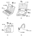
図20(A)は携帯電話であり、本体9001、音声出力部9002、音声入力部9003、表示部9004、操作スイッチ9005、アンテナ9006から構成されている。本発明は表示部9004に適用することができる
【0123】
図20(B)はビデオカメラであり、本体9101、表示部9102、音声入力部9103、操作スイッチ9104、バッテリー9105、受像部9106から成っている。本発明は表示部9102に適用することができる。
【0124】
図20(C)はパーソナルコンピュータの一種であるモバイルコンピュータ或いは携帯型情報端末であり、本体9201、カメラ部9202、受像部9203、操作スイッチ9204、表示部9205で構成されている。本発明は表示部9205に適用することができる。
【0125】
図20(D)はヘッドマウントディスプレイ(ゴーグル型ディスプレイ)であり、本体9301、表示部9302、アーム部9303で構成される。本発明は表示部9302に適用することができる。
【0126】
図20(E)はテレビであり、本体9401、スピーカ9402、表示部9403、受信装置9404、増幅装置9405等で構成される。本発明は表示部9402に適用することができる。
【0127】
図20(F)は携帯書籍であり、本体9501、表示部9502、記憶媒体9504、操作スイッチ9505、アンテナ9506から構成されており、ミニディスク(MD)やDVD(Digtial Versatile Disc)に記憶されたデータや、アンテナで受信したデータを表示するものである。本発明は表示部9502に適用することができる。
【0128】
図21(A)はパーソナルコンピュータであり、本体9601、画像入力部9602、表示部9603、キーボード9604で構成される。本発明は表示部9603に適用することができる。
【0129】
図21(B)はプログラムを記録した記録媒体(以下、記録媒体と呼ぶ)を用いるプレーヤーであり、本体9701、表示装置9702、スピーカ部9703、記録媒体9704、操作スイッチ9705で構成される。なお、この装置は記録媒体としてDVD、CD等を用い、音楽鑑賞や映画鑑賞やゲームやインターネットを行うことができる。本発明は表示部9702に適用することができる。
【0130】
図21(C)はデジタルカメラであり、本体9801、表示部9802、接眼部9803、操作スイッチ9804、受像部(図示しない)で構成される。本発明は表示部9802に適用することができる。
【0131】
図21(D)は片眼のヘッドマウントディスプレイであり、表示部9901、ヘッドマウント部9902で構成される。本発明は表示部9901に適用することができる。
【0132】
図22(A)はフロント型プロジェクターであり、投射装置3601、スクリーン3602で構成される。
【0133】
図22(B)はリア型プロジェクターであり、本体3701、投射装置3702、ミラー3703、スクリーン3704で構成される。
【0134】
なお、図22(C)は、図22(A)及び図22(B)中における投射装置3601、3702の構造の一例を示した図である。投射装置3601、3702は、光源光学系3801、ミラー3802、3804〜3806、ダイクロイックミラー3803、プリズム3807、液晶表示部3808、位相差板3809、投射光学系3810で構成される。投射光学系3810は、投射レンズを含む光学系で構成される。本実施例は三板式の例を示したが、これに限定されず、例えば単板式であってもよい。また、図22(C)中において矢印で示した光路に実施者が適宜、光学レンズや、偏光機能を有するフィルムや、位相差を調節するためのフィルム、IRフィルム等の光学系を設けてもよい。本発明は液晶表示部3808に適用することができる。
【0135】
また、図22(D)は、図22(C)中における光源光学系3801の構造の一例を示した図である。本実施例では、光源光学系3801は、リフレクター3811、光源3812、レンズアレイ3813、3814、偏光変換素子3815、集光レンズ3816で構成される。なお、図22(D)に示した光源光学系は一例であって特に限定されない。例えば、光源光学系に実施者が適宜、光学レンズや、偏光機能を有するフィルムや、位相差を調節するフィルム、IRフィルム等の光学系を設けてもよい。
【0136】
以上の様に、本発明の適用範囲はきわめて広く、画像表示装置を用いるあらゆる分野の電子機器に適用することが可能である。
【0137】
【発明の効果】
本発明のレベルシフタによれば、レベル変換動作の過渡期に生じる貫通電流を減少させ、大きな電圧振幅差間のレベル変換を容易におこなうことが可能となる。また、回路の占有面積の増加を抑制しつつ動作速度を向上させることも可能となる。このように、消費電力の小さく動作マージンの大きな本発明のレベルシフタは、歩留まりを向上させ製品コストの低減に効果的である。
【図面の簡単な説明】
【図1】 実施形態1によるレベルシフタである。
【図2】 実施形態2によるレベルシフタである。
【図3】 実施形態3によるレベルシフタである。
【図4】 実施形態4によるレベルシフタである。
【図5】 実施例1によるレベルシフタである。
【図6】 実施例1と従来例の動作比較をしたシミュレーション結果である。
【図7】 実施例1と従来例の動作遅延時間を比較したシミュレーション結果である。
【図8】 実施例2によるレベルシフタである。
【図9】 実施例3によるレベルシフタである。
【図10】 実施例3と従来例の動作比較をしたシミュレーション結果である。
【図11】 実施例4によるレベルシフタである。
【図12】 実施例5によるレベルシフタである。
【図13】 実施例6によるレベルシフタである。
【図14】 実施例7によるレベルシフタである。
【図15】 実施例8によるレベルシフタである。
【図16】 TFTの作製工程を示す断面図である。
【図17】 TFTの作製工程を示す断面図である。
【図18】 アクティブマトリクス基板断面図である。
【図19】 アクティブマトリクス型液晶表示装置の断面構造図を示す図である。
【図20】 本発明を用いた電子機器の一例を示す図である。
【図21】 本発明を用いた電子機器の一例を示す図である。
【図22】 投影型液晶表示装置の構成を示す図である。
【図23】 従来例のレベルシフタの一例である。
【図24】 従来例のレベルシフタの一例である。
【符号の説明】
10a(〜d) 電圧調整回路
101〜104 PチャネルMOSトランジスタ
105〜110 NチャネルMOSトランジスタ
111〜114 PチャネルMOSトランジスタ
115〜118 NチャネルMOSトランジスタ
119〜120 PチャネルMOSトランジスタ[0001]
BACKGROUND OF THE INVENTION
[0002]
The present invention relates to a level shifter used in a drive circuit of an image display device (active matrix image display device) that displays information such as video using switching elements and pixels arranged in a matrix.
[0003]
[Prior art]
In recent years, miniaturization of semiconductor manufacturing technology has progressed, and low power consumption is required such as LSIs for portable devices, and LSIs driven by a low power supply voltage of 3.3 V have become mainstream.
[0004]
On the other hand, liquid crystal displays, which are recently in high demand for applications such as portable terminals and computer monitors, perform liquid crystal driving with a signal having a voltage amplitude of 10 to 20 V, and thus operate at a high power supply voltage corresponding to the driving circuit. There is at least a circuit section.
[0005]
Therefore, a level shifter for converting the voltage amplitude is indispensable between the low voltage amplitude signal of the controller LSI and the high voltage amplitude signal necessary for driving the liquid crystal display.
[0006]
A conventional level shifter widely used is shown in FIG. This converts a signal having a voltage amplitude of 0 to VDD1 (> 0, for example, 5V) into a signal having a voltage amplitude of 0 to VDD2 (> VDD1, for example, 10V), that is, the low potential side is fixed and the high potential side is fixed. A level shifter to be shifted. The structure of this level shifter is as follows. The power source VDD2 is connected to the source of a P-channel MOS transistor (hereinafter abbreviated as PMOST) 101 and the source of PMOST102, the drain of PMOST101 is connected to the source of PMOST103, and the drain of PMOST102 is connected to the source of PMOST104. Further, the drain of the
[0007]
In the present specification, a power supply whose power supply voltage is VDD # is referred to as power supply VDD #. In addition, GND, VDD1, VDD2, VDD3, and VDD4 are handled as five types of power supply voltages.
VDD4 <VDD3 <GND <VDD1 <VDD2
Shall be satisfied. However, for ease of explanation, GND is set to 0V.
[0008]
Next, the basic operation of this conventional level shifter will be described. When the potential of the input signal (IN) is “Hi” of VDD1, the NMOS T105 is turned on and the PMOST103 is turned off. Therefore, the gate of the PMOST102 is inputted with “Lo” with the potential GND, and the PMOST102 is turned on. On the other hand, since the potential of the inverting input signal (/ IN) is “Lo” with GND, the
[0009]
When the potential of the input signal (IN) is “Lo” of GND, the level shifter shown in FIG. 23 has a symmetrical structure, so that it can be understood in the same manner as described above. From the output terminal (OUT), the potential is GND (0 V). “Lo” is output.
[0010]
In this way, a signal having a voltage amplitude of 0 to VDD1 is converted into a signal having a voltage amplitude of 0 to VDD2.
[0011]
Next, FIG. 24 shows a conventional level shifter in which the high potential side is fixed and the low potential side is shifted. This converts a signal having a voltage amplitude of VDD3 (<0) to 0 into a signal having a voltage amplitude of VDD4 (<VDD3) to 0. The structure of this level shifter is as follows. The source of the NMOST 107 and the source of the NMOST 108 are connected to the
[0012]
Next, the basic operation of the conventional level shifter shown in FIG. 24 will be described. When the potential of the input signal (IN) is “Lo” of VDD 3, the PMOST 111 is turned on and the NMOST 109 is turned off. Therefore, the gate of the
[0013]
When the potential of the input signal (IN) is “Hi” of GND, the level shifter shown in FIG. 24 has a symmetrical structure, so that it can be understood in the same manner as described above. From the output terminal (OUT), the potential is “Hi” of GND. Is output.
[0014]
In this way, a signal having a voltage amplitude of VDD3-0 is converted into a signal having a voltage amplitude of VDD4-0.
[0015]
[Problems to be solved by the invention]
In the conventional level shifter described above, level conversion between small voltage amplitude differences can be performed relatively easily. However, level conversion becomes more difficult and problematic as the voltage amplitude difference becomes larger. . Hereinafter, these problems will be described.
[0016]
The basic operation of the level shifter of the conventional example has been briefly described above. However, depending on the voltage amplitude to be converted, the characteristics of the transistor, and the like, the availability of operation and the operation time are determined. In the level shifter shown in FIG. 23, for example, VDD1 = 5V, VDD2 = 15V, threshold voltages of
[0017]
1) Method of turning off the
In order to turn off the
[0018]
2) Method of turning off the
In order to turn off the
[0019]
In any case, in the above two methods, the
[0020]
When the input signal (IN) changes from “Hi” having a potential of 5V to “Lo” having a potential of 0V, the roles of the
[0021]
As described above, with respect to the level shifter of the conventional example of FIG. 23, it is important that the
[0022]
The same applies to the level shifter of the conventional example of FIG.
[0023]
Therefore, the present invention reduces the power consumption due to the through current generated in the transition period of operation, facilitates level conversion between large voltage amplitude differences, and increases the occupied area of the circuit while improving the operation speed. A level shifter to be suppressed is newly provided.
[0024]
[Means for Solving the Problems]
A level shifter according to an aspect of the present invention includes a first conductivity type first MOS transistor having a source connected to a first power source and a gate to which a first input signal is input, A second MOS transistor having the same conductivity type as the first conductivity type, having a source connected to a power source and a gate to which a second input signal that is an inverted signal of the first input signal is input; Have
[0025]
Further, a second conductivity type having a drain connected to a drain of the first MOS transistor and a gate to which the first input signal is input is a conductivity type different from the first conductivity type. A third MOS transistor, a drain connected to the drain of the second MOS transistor, and a gate to which the second input signal is input; And a MOS transistor.
[0026]
A fifth MOS transistor having the same conductivity type as the second conductivity type, further comprising a drain connected to the source of the third MOS transistor and a gate connected to the drain of the second MOS transistor; A sixth MOS transistor having the same conductivity type as the second conductivity type, having a drain connected to the source of the fourth MOS transistor and a gate connected to the drain of the first MOS transistor; Have
[0027]
Further, the first voltage adjustment circuit connected between the source of the fifth MOS transistor and the second power supply is connected between the source of the sixth MOS transistor and the second power supply. And a second voltage adjustment circuit.
[0028]
The level shifter converts the first and second input signals having a first voltage amplitude into a signal having a second voltage amplitude, and converts the first MOS transistor drain and the second MOS transistor drain to each other. Output from at least one. The two voltage adjustment circuits facilitate level conversion between large voltage amplitude differences by adjusting the source potential of the fifth MOS transistor and the source potential of the sixth MOS transistor in the transition period of the level conversion operation. To solve the above problems.
[0029]
According to another aspect of the present invention, a level shifter includes: a first MOS transistor of a first conductivity type having a source connected to a first power source; and a gate to which a first input signal is input; A second MOS transistor of the same conductivity type as the first conductivity type, having a source connected to one power source and a gate to which a second input signal that is an inverted signal of the first input signal is input And having.
[0030]
Further, the second conductivity having a drain connected to the drain of the first MOS transistor and a gate connected to the drain of the second MOS transistor, which is a conductivity type different from the first conductivity type. The same conductivity type as the second conductivity type, having a third MOS transistor of the type, a drain connected to the drain of the second MOS transistor, and a gate connected to the drain of the first MOS transistor And a fourth MOS transistor.
[0031]
Further, the first voltage adjustment circuit connected between the source of the third MOS transistor and the second power supply is connected between the source of the fourth MOS transistor and the second power supply. And a second voltage adjustment circuit.
[0032]
The level shifter converts the first and second input signals having a first voltage amplitude into a signal having a second voltage amplitude, and converts the first MOS transistor drain and the second MOS transistor drain to each other. Output from at least one. The two voltage adjustment circuits adjust the source potential of the third MOS transistor and the source potential of the fourth MOS transistor in a transition period of level conversion operation, thereby facilitating level conversion between large voltage amplitude differences. To solve the above problems.
[0033]
The voltage adjustment circuit may include a MOS transistor having a drain and a gate connected to each other.
[0034]
The voltage regulator circuit may include a resistor including a silicon layer or a polysilicon layer doped with impurities.
[0035]
The voltage adjusting circuit may include a MOS transistor having a constant voltage applied to the gate.
[0036]
DETAILED DESCRIPTION OF THE INVENTION
Hereinafter, embodiments of the present invention will be described with reference to the drawings. In order to facilitate comparison with the conventional example, the same reference numerals are used for the transistors and the like corresponding to the respective parts of the conventional example in the following description of the embodiment.
[0037]
[Embodiment 1]
In the present embodiment, a level shifter of the form shown in FIG. 1 in which the low potential side of the signal is fixed and the high potential side is shifted will be described. In the configuration, first, two elements (10a, 10b) are connected to a power source VDD2 (>VDD1> 0), or two elements or circuits (hereinafter referred to as voltage adjustment circuits) that generate a potential difference when a current flows. The
[0038]
With these
[0039]
[Embodiment 2]
In the present embodiment, a level shifter of the form shown in FIG. 2 will be described in which the high potential side of the signal is fixed and the low potential side is shifted. In the configuration, first, the first terminals of the two
[0040]
With these
[0041]
[Embodiment 3]
In the present embodiment, a level shifter of the form shown in FIG. 3 different from the first embodiment in which the low potential side of the signal is fixed and the high potential side is shifted will be described. In the configuration, first, the first terminals of the two
[0042]
With these
[0043]
[Embodiment 4]
In the present embodiment, a level shifter of the form shown in FIG. 4 different from the second embodiment in which the high potential side of the signal is fixed and the low potential side is shifted will be described. In the configuration, first, the first terminals of the two
[0044]
With these
[0045]
【Example】
Now, embodiments of the present invention will be described with reference to the drawings.
[0046]
[Example 1]
In this embodiment, the level shifter shown in FIG. 5 will be described in which the low potential side of the signal is fixed and the high potential side is shifted. Note that this example is an example in which a specific example of the voltage adjustment circuit is clearly shown in the first embodiment. Further, this embodiment can be said to be an improved version of the conventional example shown in FIG. 23, and the same reference numerals are used for the transistors corresponding to the respective parts.
[0047]
The configuration of the level shifter of this embodiment is as follows. The source of the
[0048]
Subsequently, the operation of the level shifter of this embodiment will be described. However, since the
[0049]
In the level shifter shown in FIG. 5, for example, VDD1 = 5V, VDD2 = 15V, threshold voltages of the
[0050]
Next, consider what happens when the input signal (IN) becomes “Hi” with a potential of 5 V from this state. Also at this time, the
[0051]
These states can be confirmed by the simulation results shown in FIG. In the figure, the result of the conventional example is also indicated by white marks. The main parameters of the transistors used in the simulation are the threshold voltage and mobility of all PMOSTs of −2 V and 100 cm, respectively. 2 / Vs, and threshold voltage and mobility of all NMOSTs are 2V and 100cm, respectively. 2 / Vs. The channel lengths of the transistors were all 4 μm, and the channel widths were 10 μm for the
[0052]
Further, the channel width (W) of the
[0053]
FIG. 7B shows the result of simulating the delay time (Td) when the power supply voltage VDD2 is changed. However, the delay time in this case is the time from when the input signal (IN) rises 50% to when the output signal (OUT) rises 50% of the power supply voltage VDD2. The mobility, threshold value, etc. used in the simulation at this time were the same as described above, and the channel widths were 10 μm for the
[0054]
When the input signal (IN) changes from “Hi” at a potential of 5 V to “Lo” at a potential of 0 V, the roles of the
[0055]
[Example 2]
In this embodiment, another example of the level shifter that shifts the high potential side while the low potential side of the signal is fixed will be described. As shown in FIG. 8, the level shifter of this embodiment is obtained by replacing the
[0056]
The configuration of the level shifter of this embodiment is as follows. The drain and gate of the
[0057]
The operation of the level shifter of this embodiment is basically the same as that of the first embodiment, and the roles of the
[0058]
As described above, the level shifter of the present embodiment, like the first embodiment, facilitates level conversion between large level differences compared to the conventional example, improves the operation speed, reduces the through current, and reduces the power consumption. Is effective. In addition, it is resistant to variations in transistor characteristics. In this embodiment, if the transistor is formed so that the threshold voltage of NMOS is smaller than the absolute value of the threshold voltage of PMOST, the logic circuit of the next stage for inputting the output signal of the level shifter of this embodiment A sufficient margin for turning off the PMOST can be provided.
[0059]
[Example 3]
In the present embodiment, the level shifter shown in FIG. 9 is described in which the high potential side of the signal is fixed and the low potential side is shifted. This example is an example in which a specific example of the voltage adjustment circuit is clearly shown in the second embodiment. Further, this embodiment can be said to be an improved version of the conventional example shown in FIG. 24, and the same reference numerals are used for the transistors corresponding to the respective parts.
[0060]
The configuration of the level shifter of this embodiment is as follows. The source of the NMOS T117 and the source of the NMOS T118 are connected to the power supply VDD4. The gate and drain of the NMOS T117 are connected to the source of the NMOS T107, and the gate and drain of the NMOS T118 are connected to the source of the NMOS T108. The drain of the NMOS T107 is connected to the source of the NMOS T109, and the drain of the NMOS T108 is connected to the source of the NMOS T110. The drain of the NMOS T109 is connected to the gate of the NMOS T108 and the drain of the PMOST111, the drain of the NMOST110 is connected to the gate of the NMOST107 and the drain of the PMOST112, and the source of the PMOST111 and the source of the PMOST112 are connected to GND (0V). An input signal (IN) having a voltage amplitude of VDD3 to 0 is supplied to the gates of NMOST109 and PMOST111, and an inverted input signal (/ IN) of the same voltage amplitude is input to the gates of NMOST110 and PMOST112. The output signal (OUT) whose level is converted is extracted from the drain of the
[0061]
Subsequently, the operation of the level shifter of this embodiment will be described. However, since the
[0062]
In the level shifter shown in FIG. 9, for example, VDD3 = −5V, VDD4 = −15V, threshold voltages of
[0063]
Next, consider what happens when the input signal (IN) becomes “Lo” with a potential of −5 V from this state. Also at this time, immediately after the change of the input signal, the
[0064]
These states can be confirmed by the simulation results shown in FIG. In the figure, the result of the conventional example is also indicated by white marks. The main parameters of the transistors used in the simulation are the threshold voltage and mobility of all PMOSTs of −2 V and 100 cm, respectively. 2 / Vs, and threshold voltage and mobility of all NMOSTs are 2V and 100cm, respectively. 2 / Vs. The channel lengths of the transistors were all 4 μm, and the channel widths were 10 μm for the
[0065]
When the input signal (IN) changes from “Lo” having a potential of −5V to “Hi” having a potential of 0V, the roles of the
[0066]
[Example 4]
Also in this embodiment, another example of a level shifter that shifts the low potential side while the high potential side of the signal is fixed will be described. As shown in FIG. 11, the level shifter of the present embodiment is obtained by replacing
[0067]
The configuration of the level shifter of this embodiment is as follows. The power source VDD4 is connected to the drain and gate of the PMOST119, the drain and gate of the PMOST120, the source of the PMOST119 is connected to the source of the NMOST107, and the source of the PMOST120 is connected to the source of the NMOST108. The drain of the NMOS T107 is connected to the source of the NMOS T109, and the drain of the NMOS T108 is connected to the source of the NMOS T110. The drain of the NMOS T109 is connected to the gate of the NMOST108 and the drain of the PMOST111, the drain of the NMOST110 is connected to the gate of the NMOST107 and the drain of the PMOST112, and the source of the PMOST111 and the source of the PMOST112 are connected to GND (0V). An input signal (IN) having a voltage amplitude of VDD3 to 0 is supplied to the gates of NMOST109 and PMOST111, and an inverted input signal (/ IN) of the same voltage amplitude is input to the gates of NMOST110 and PMOST112. The output signal (OUT) whose level is converted is extracted from the drain of the
[0068]
The operation of the level shifter of this embodiment is basically the same as that of the third embodiment, and the roles of the
[0069]
As described above, the level shifter of the present embodiment, like the third embodiment, facilitates level conversion between large level differences compared to the conventional example, improves the operation speed, reduces the through current, and reduces the power consumption. Is effective. In addition, it is resistant to variations in transistor characteristics. In this embodiment, if the transistor is formed so that the absolute value of the PMOS threshold voltage is smaller than the threshold voltage of the NMOST, the logic circuit of the next stage for inputting the output signal of the level shifter of this embodiment A sufficient margin for turning off the NMOST can be provided.
[0070]
[Example 5]
In this embodiment, the level shifter shown in FIG. 12 will be described in which the low potential side of the signal is fixed and the high potential side is shifted. Note that this example is an example in which a specific example of the voltage adjustment circuit is clearly shown in the third embodiment. Further, this embodiment can be said to be an improved version of the first embodiment shown in FIG. 5, and the same reference numerals are used for the transistors corresponding to the respective parts.
[0071]
The configuration of the level shifter of this embodiment is as follows. The source of the
[0072]
The level shifter of this embodiment is basically the same as that of the first embodiment in operation, and is obtained by deleting the
[0073]
As described above, the level shifter of the present embodiment, like the first embodiment, facilitates level conversion between large level differences compared to the conventional example, improves the operation speed, reduces the through current, and reduces the power consumption. Is effective. In addition, it is resistant to variations in transistor characteristics. Since this embodiment is composed of the same number of transistors as the conventional example, the area occupied by the circuit can be reduced if the level shifter has the same operating characteristics.
[0074]
[Example 6]
In this embodiment, another example of the level shifter that shifts the high potential side while the low potential side of the signal is fixed will be described. As shown in FIG. 13, the level shifter of this embodiment is obtained by replacing
[0075]
The configuration of the level shifter of this embodiment is as follows. The drain and gate of the
[0076]
The level shifter of the present embodiment is basically the same as the second embodiment in operation, and is obtained by deleting the
[0077]
As described above, the level shifter of the present embodiment, like the second embodiment, facilitates level conversion between large level differences compared to the conventional example, improves the operation speed, reduces the through current, and reduces the power consumption. Is effective. In addition, it is resistant to variations in transistor characteristics. In this embodiment, if the transistor is formed so that the threshold voltage of NMOS is smaller than the absolute value of the threshold voltage of PMOST, the logic circuit of the next stage for inputting the output signal of the level shifter of this embodiment A sufficient margin for turning off the PMOST can be provided. Since this embodiment is composed of the same number of transistors as the conventional example, the area occupied by the circuit can be reduced if the level shifter has the same operating characteristics.
[0078]
[Example 7]
In this embodiment, a level shifter shown in FIG. 14 is described in which the high potential side of the signal is fixed and the low potential side is shifted. This example is an example in which a specific example of the voltage adjustment circuit is clearly shown in the fourth embodiment. Further, this embodiment can be said to be an improved version of the embodiment 3 shown in FIG. 9, and the same reference numerals are used for transistors corresponding to the respective parts.
[0079]
The configuration of the level shifter of this embodiment is as follows. The source of NMOS T117 and the source of NMOS T118 are connected to power source VDD4, the gate and drain of NMOS T117 are connected to the source of NMOS T107, and the gate and drain of NMOS T118 are connected to the source of NMOS T108, respectively. The drain of the NMOS T107 is connected to the gate of the NMOS T108 and the drain of the PMOST111, and the drain of the NMOST108 is connected to the gate of the NMOST107 and the drain of the PMOST112. The source of the
[0080]
The operation of the level shifter of this embodiment is basically the same as that of the third embodiment, and the
[0081]
As described above, the level shifter of the present embodiment, like the third embodiment, facilitates level conversion between large level differences compared to the conventional example, improves the operation speed, reduces the through current, and reduces the power consumption. Is effective. In addition, it is resistant to variations in transistor characteristics. Since this embodiment is composed of the same number of transistors as the conventional example, the area occupied by the circuit can be reduced if the level shifter has the same operating characteristics.
[0082]
[Example 8]
Also in this embodiment, another example of a level shifter that shifts the low potential side while the high potential side of the signal is fixed will be described. As shown in FIG. 15, the level shifter of this embodiment is obtained by replacing the
[0083]
The configuration of the level shifter of this embodiment is as follows. The drain and gate of the PMOST119 and the drain and gate of the PMOST120 are connected to the power supply VDD4, respectively, the source of the PMOST119 is connected to the source of the NMOST107, and the source of the PMOST120 is connected to the source of the NMOST108. The drain of the NMOS T107 is connected to the gate of the NMOS T108 and the drain of the PMOST111, and the drain of the NMOST108 is connected to the gate of the NMOST107 and the drain of the PMOST112. The source of the
[0084]
The operation of the level shifter of this embodiment is basically the same as that of the fourth embodiment, and the
[0085]
As described above, the level shifter of this embodiment, like the fourth embodiment, facilitates level conversion between large level differences compared to the conventional example, improves the operation speed, reduces the through current, and reduces the power consumption. Is effective. In addition, it is resistant to variations in transistor characteristics. In this embodiment, if the transistor is formed so that the absolute value of the PMOS threshold voltage is smaller than the threshold voltage of the NMOST, the next stage logic circuit for inputting the output signal of the level shifter of this embodiment A sufficient margin for turning off the NMOST can be provided. Since this embodiment is composed of the same number of transistors as the conventional example, the area occupied by the circuit can be reduced if the level shifter has the same operating characteristics.
[0086]
[Example 9]
In this example, a level shifter using a resistor as a voltage adjustment circuit in Embodiments 1 to 4 will be described. As this resistance, a method in which the gate of the transistor is biased above its threshold voltage and is always turned on to use the source-drain region as a resistance, a method in which the source-drain region of the transistor is used, and an LDD region There is a method of using. Using these resistors also has an effect of facilitating the level conversion operation. In this case, the output amplitude of the level shifter does not vary by the threshold voltage as in the first to ninth embodiments, and becomes full scale.
[Example 10]
In this embodiment, an example of a production method when the level shifters of Embodiments 1 to 9 are applied to a drive circuit of an active matrix liquid crystal display device will be described. Note that a pixel TFT which is a switching element of the pixel portion and a TFT of a driver circuit (a signal line driver circuit, a scanning line driver circuit, or the like) having a level shifter of the present invention provided around the pixel portion are manufactured over the same substrate. Take up the process. However, for ease of explanation, a CMOS circuit, which is a basic configuration circuit, is illustrated in the driving circuit portion, and an n-channel TFT is illustrated in a cross section along a certain path as the pixel TFT of the pixel portion. To do.
[0087]
First, as shown in FIG. 16A, a silicon oxide film on a
[0088]
The island-shaped semiconductor layers 402 to 406 are formed using a crystalline semiconductor film in which a semiconductor film having an amorphous structure is formed using a laser crystallization method or a known thermal crystallization method. The island-like semiconductor layers 402 to 406 are formed to have a thickness of 25 to 80 nm (preferably 30 to 60 nm). There is no limitation on the material of the crystalline semiconductor film, but the crystalline semiconductor film is preferably formed of silicon or a silicon germanium (SiGe) alloy.
[0089]
In order to fabricate a crystalline semiconductor film by laser crystallization, a pulse oscillation type or continuous emission type excimer laser, YAG laser, YVO Four Use a laser. When these lasers are used, it is preferable to use a method in which laser light emitted from a laser oscillator is linearly collected by an optical system and irradiated onto a semiconductor film. Crystallization conditions are appropriately selected by the practitioner. When an excimer laser is used, the pulse oscillation frequency is 30 Hz and the laser energy density is 100 to 400 mJ / cm. 2 (Typically 200-300mJ / cm 2 ). When a YAG laser is used, the second harmonic is used and the pulse oscillation frequency is 1 to 10 kHz, and the laser energy density is 300 to 600 mJ / cm. 2 (Typically 350-500mJ / cm 2 ) Then, a laser beam condensed linearly with a width of 100 to 1000 μm, for example 400 μm, is irradiated over the entire surface of the substrate, and the superposition rate (overlap rate) of the linear laser beam at this time is 80 to 98%.
[0090]
Next, a
[0091]
Then, a first
[0092]
The Ta film is formed by sputtering, and a Ta target is sputtered with Ar. In this case, when an appropriate amount of Xe or Kr is added to Ar, the internal stress of the Ta film can be relieved and peeling of the film can be prevented. The resistivity of the α-phase Ta film is about 20 μΩcm and can be used for the gate electrode, but the resistivity of the β-phase Ta film is about 180 μΩcm and is not suitable for the gate electrode. In order to form an α-phase Ta film, tantalum nitride having a crystal structure close to Ta's α-phase is formed on a Ta base with a thickness of about 10 to 50 nm, so that an α-phase Ta film can be easily obtained. be able to.
[0093]
When forming a W film, it is formed by sputtering using W as a target. In addition, tungsten hexafluoride (WF 6 It can also be formed by a thermal CVD method using In any case, in order to use as a gate electrode, it is necessary to reduce the resistance, and the resistivity of the W film is desirably 20 μΩcm or less. The resistivity of the W film can be reduced by increasing the crystal grains. However, when there are many impurity elements such as oxygen in W, crystallization is hindered and the resistance is increased. Therefore, in the case of sputtering, the resistivity is obtained by using a W target with a purity of 99.9999% and forming a W film with sufficient consideration so that impurities are not mixed in the gas phase during film formation. 9-20 μΩcm can be realized.
[0094]
Note that in this embodiment, the first
[0095]
Next, resist
[0096]
Under the above etching conditions, by making the shape of the resist mask suitable, the end portions of the first conductive layer and the second conductive layer have an angle of taper of 15 due to the effect of the bias voltage applied to the substrate side. It becomes a taper shape of ˜45 °. In order to perform etching without leaving a residue on the gate insulating film, it is preferable to increase the etching time at a rate of about 10 to 20%. Since the selection ratio of the silicon oxynitride film to the W film is 2 to 4 (typically 3), the surface where the silicon oxynitride film is exposed is etched by about 20 to 50 nm by the over-etching process. Thus, the first shape
[0097]
Then, a first doping process is performed, and an impurity element imparting n-type conductivity is added. (FIG. 16B) The doping method may be an ion doping method or an ion implantation method. The condition of the ion doping method is a dose of 1 × 10 13 ~ 5x10 14 atoms / cm 2 The acceleration voltage is set to 60 to 100 keV. As an impurity element imparting n-type, an element belonging to
[0098]
Next, a second etching process is performed as shown in FIG. Similarly, using the ICP etching method, the etching gas is CF. Four And Cl 2 And O 2 And 500 W of RF power (13.56 MHz) is supplied to the coil-type electrode at a pressure of 1 Pa to generate plasma. 50 W RF (13.56 MHz) power is applied to the substrate side (sample stage), and a lower self-bias voltage is applied than in the first etching process. Under such conditions, the W film is anisotropically etched, and Ta, which is the first conductive layer, is anisotropically etched at a slower etching rate to form the second shape
[0099]
CF of W film and Ta film Four And Cl 2 The etching reaction by the mixed gas can be estimated from the generated radicals or ion species and the vapor pressure of the reaction product. Comparing the vapor pressure of fluoride and chloride of W and Ta, WF, which is fluoride of W 6 Is extremely high, other WCl Five , TaF Five , TaCl Five Are comparable. Therefore, CF Four And Cl 2 With this mixed gas, both the W film and the Ta film are etched. However, an appropriate amount of O is added to this mixed gas. 2 When CF is added Four And O 2 Reacts to CO and F, and a large amount of F radicals or F ions are generated. As a result, the etching rate of the W film having a high fluoride vapor pressure is increased. On the other hand, the increase in etching rate of Ta is relatively small even when F increases. Further, since Ta is more easily oxidized than W, O 2 When Ta is added, the surface of Ta is oxidized. Since the Ta oxide does not react with fluorine or chlorine, the etching rate of the Ta film further decreases. Therefore, it is possible to make a difference in the etching rate between the W film and the Ta film, and the etching rate of the W film can be made larger than that of the Ta film.
[0100]
Then, a second doping process is performed as shown in FIG. In this case, an impurity element imparting n-type conductivity is doped as a condition of a high acceleration voltage by lowering the dose than in the first doping process. For example, the acceleration voltage is 70 to 120 keV and 1 × 10 13 /cm 2 A new impurity region is formed inside the first impurity region formed in the island-shaped semiconductor layer in FIG. Doping is performed using the second shape
[0101]
Then, as shown in FIG. 17B,
[0102]
Through the above steps, an impurity region is formed in each island-shaped semiconductor layer.
[0103]
Thus, for the purpose of controlling the conductivity type, as shown in FIG. 17C, a step of activating the impurity element added to each island-like semiconductor layer is performed. This step is performed by a thermal annealing method using a furnace annealing furnace. In addition, a laser annealing method or a rapid thermal annealing method (RTA method) can be applied. In the thermal annealing method, the oxygen concentration is 1 ppm or less, preferably 0.1 ppm or less in a nitrogen atmosphere at 400 to 700 ° C., typically 500 to 600 ° C. In this example, the temperature is 500 ° C. for 4 hours. Heat treatment is performed. However, when the wiring material used for 433 to 440 is weak against heat, activation is preferably performed after an interlayer insulating film (mainly composed of silicon) is formed in order to protect the wiring and the like.
[0104]
Further, a heat treatment is performed at 300 to 450 ° C. for 1 to 12 hours in an atmosphere containing 3 to 100% hydrogen to perform a step of hydrogenating the island-shaped semiconductor layer. This step is a step of terminating dangling bonds in the semiconductor layer with thermally excited hydrogen. As another means of hydrogenation, plasma hydrogenation (using hydrogen excited by plasma) may be performed.
[0105]
Next, the first
[0106]
In the driver circuit portion, source wirings 459 to 461 that form contacts with the source region of the island-like semiconductor layer (the portion corresponding to the source of the TFT), and drains that form the contact with the drain region (the portion corresponding to the drain of the TFT)
[0107]
As described above, the driver circuit portion including the n-channel TFT 501, the p-channel TFT 502, and the n-channel TFT 503, and the pixel portion including the pixel TFT 504 and the storage capacitor 505 can be formed over the same substrate. In this specification, such a substrate is referred to as an active matrix substrate for convenience.
[0108]
The n-channel TFT 501 in the driver circuit portion includes a
[0109]
The pixel TFT 504 in the pixel portion includes a
[0110]
In this embodiment, the end portions of the pixel electrodes are arranged so as to overlap the signal lines and the scanning lines so that the gaps between the pixel electrodes can be shielded without using a black matrix.
[0111]
Further, according to the steps shown in this embodiment, the number of photomasks necessary for the production of the active matrix substrate is 5 (island-like semiconductor layer pattern, first wiring pattern (scanning line, signal line, capacitive wiring), n The mask pattern of the channel region, the contact hole pattern, and the second wiring pattern (including the pixel electrode and the connection electrode) can be used. As a result, the process can be shortened, and the manufacturing cost can be reduced and the yield can be improved.
[0112]
[Example 11]
In this embodiment, a process of manufacturing an active matrix liquid crystal display device from the active matrix substrate manufactured in
[0113]
First, after obtaining the active matrix substrate in the state of FIG. 18 according to Example 10, an
[0114]
On the other hand, a
[0115]
In addition, a red
[0116]
The arrangement of the spacers may be arbitrarily determined. For example, as shown in FIG. 19, the spacers may be arranged on the counter substrate so as to be positioned on the connection electrodes. In addition, a spacer may be arranged on the counter substrate with its position aligned on the TFT of the driver circuit portion. This spacer may be disposed over the entire surface of the drive circuit portion, or may be disposed so as to cover the source wiring and the drain wiring.
[0117]
After the
[0118]
Then, the active matrix substrate on which the pixel portion and the driver circuit portion are formed and the counter substrate are bonded together with a
[0119]
Note that the TFT formed by the above process has a top gate structure, but the present invention can be applied to a TFT having a bottom gate structure and other structures.
[0120]
The present invention can also be applied to an EL display device that is a self-luminous image display device using electroluminescence (EL) instead of liquid crystal.
[0121]
[Example 12]
In this embodiment, an electronic device incorporating an active matrix liquid crystal display device or an EL display device using the level shifter of the present invention will be described. Examples of these electronic devices include portable information terminals (electronic notebooks, mobile computers, mobile phones, etc.), video cameras, still cameras, personal computers, televisions, and the like. Examples of these are shown in FIGS. However, FIGS. 20, 21, and 22 are applied to the active matrix liquid crystal display device, and FIGS. 20 and 21 are applied to the EL display device.
[0122]
FIG. 20A illustrates a mobile phone, which includes a main body 9001, an
[0123]
FIG. 20B illustrates a video camera which includes a main body 9101, a
[0124]
FIG. 20C illustrates a mobile computer or portable information terminal which is a kind of personal computer, which includes a main body 9201, a camera portion 9202, an
[0125]
FIG. 20D illustrates a head mounted display (goggles type display), which includes a main body 9301, a
[0126]
FIG. 20E illustrates a television set including a main body 9401, a
[0127]
FIG. 20F illustrates a portable book, which includes a main body 9501, a
[0128]
FIG. 21A illustrates a personal computer, which includes a main body 9601, an
[0129]
FIG. 21B shows a player that uses a recording medium (hereinafter referred to as a recording medium) on which a program is recorded, and includes a main body 9701, a
[0130]
FIG. 21C illustrates a digital camera which includes a main body 9801, a
[0131]
FIG. 21D illustrates a one-eye head mounted display which includes a display portion 9901 and a
[0132]
FIG. 22A illustrates a front type projector, which includes a
[0133]
FIG. 22B illustrates a rear projector, which includes a main body 3701, a
[0134]
Note that FIG. 22C illustrates an example of the structure of the
[0135]
FIG. 22D illustrates an example of the structure of the light source optical system 3801 in FIG. In this embodiment, the light source optical system 3801 includes a reflector 3811, a light source 3812, lens arrays 3813 and 3814, a polarization conversion element 3815, and a condenser lens 3816. Note that the light source optical system illustrated in FIG. 22D is an example and is not particularly limited. For example, the practitioner may appropriately provide an optical system such as an optical lens, a film having a polarization function, a film for adjusting a phase difference, or an IR film in the light source optical system.
[0136]
As described above, the applicable range of the present invention is extremely wide and can be applied to electronic devices in various fields using an image display device.
[0137]
【The invention's effect】
According to the level shifter of the present invention, it is possible to reduce the through current generated in the transition period of the level conversion operation and easily perform the level conversion between large voltage amplitude differences. It is also possible to improve the operation speed while suppressing an increase in the area occupied by the circuit. Thus, the level shifter of the present invention with low power consumption and large operation margin is effective in improving yield and reducing product cost.
[Brief description of the drawings]
FIG. 1 is a level shifter according to a first embodiment.
FIG. 2 is a level shifter according to a second embodiment.
FIG. 3 is a level shifter according to a third embodiment.
FIG. 4 is a level shifter according to a fourth embodiment.
5 is a level shifter according to Embodiment 1. FIG.
FIG. 6 is a simulation result comparing the operation of Example 1 and a conventional example.
FIG. 7 is a simulation result comparing the operation delay times of Example 1 and a conventional example.
8 is a level shifter according to Embodiment 2. FIG.
9 is a level shifter according to Embodiment 3. FIG.
FIG. 10 is a simulation result of operation comparison between Example 3 and a conventional example.
FIG. 11 shows a level shifter according to a fourth embodiment.
12 is a level shifter according to
13 is a level shifter according to Embodiment 6. FIG.
14 is a level shifter according to Embodiment 7. FIG.
15 is a level shifter according to Embodiment 8. FIG.
FIG. 16 is a cross-sectional view showing a manufacturing process of a TFT.
FIG. 17 is a cross-sectional view showing a manufacturing process of a TFT.
FIG. 18 is a cross-sectional view of an active matrix substrate.
FIG. 19 is a diagram showing a cross-sectional structure diagram of an active matrix liquid crystal display device.
FIG. 20 is a diagram showing an example of an electronic apparatus using the present invention.
FIG. 21 is a diagram showing an example of an electronic apparatus using the present invention.
FIG. 22 is a diagram showing a configuration of a projection type liquid crystal display device.
FIG. 23 is an example of a conventional level shifter.
FIG. 24 is an example of a conventional level shifter.
[Explanation of symbols]
10a (-d) Voltage adjustment circuit
101-104 P-channel MOS transistor
105-110 N-channel MOS transistor
111-114 P-channel MOS transistor
115-118 N-channel MOS transistor
119-120 P-channel MOS transistor
Claims (18)
ソースが前記第1の電源に電気的に接続され、ゲートに前記第1の入力信号の反転信号である第2の入力信号が入力される、前記第1のMOSトランジスタと同じ導電形式の第2のMOSトランジスタと、
ドレインが前記第1のMOSトランジスタのドレインに電気的に接続され、ゲートに前記第1の入力信号が入力される、前記第1のMOSトランジスタとは逆の導電形式である第3のMOSトランジスタと、
ドレインが前記第2のMOSトランジスタのドレインに電気的に接続され、ゲートに前記第2の入力信号が入力される、前記第3のMOSトランジスタと同じ導電形式の第4のMOSトランジスタと、
ドレインが前記第3のMOSトランジスタのソースに電気的に接続され、ゲートが前記第2のMOSトランジスタのドレインに電気的に接続される、前記第3のMOSトランジスタと同じ導電形式の第5のMOSトランジスタと、
ドレインが前記第4のMOSトランジスタのソースに電気的に接続され、ゲートが前記第1のMOSトランジスタのドレインに電気的に接続される、前記第3のMOSトランジスタと同じ導電形式の第6のMOSトランジスタと、
ドレインが前記第5のMOSトランジスタのソースに電気的に接続され、ソースが第2の電源に電気的に接続される、前記第1のMOSトランジスタと逆の導電形式の第7のMOSトランジスタを有する電圧調節回路と、
ドレインが前記第6のMOSトランジスタのソースに電気的に接続され、ソースが前記第2の電源に電気的に接続される、前記第1のMOSトランジスタと逆の導電形式の第8のMOSトランジスタを有する電圧調節回路と、
を有し、
前記第7のMOSトランジスタのゲートと前記第7のMOSトランジスタの前記ドレインが電気的に接続され、
前記第8のMOSトランジスタのゲートと前記第8のMOSトランジスタの前記ドレインが電気的に接続されることを特徴とするレベルシフタ。A first MOS transistor having a source electrically connected to a first power supply and a gate receiving a first input signal;
Source electrically connected to said first power supply, a second of the same conductivity type as the second input signal are entered, the first MOS transistor is an inverted signal of the gate first input signal MOS transistors of
The drain is electrically connected to the drain of said first MOS transistor, a third MOS transistor, wherein the gate first input signal are entered, and the first MOS transistor is opposite conductivity type ,
The drain is electrically connected to the drain of said second MOS transistor, wherein the gate the second input signal are entered, and a fourth MOS transistor of the same conductivity type as the third MOS transistor,
Drain is electrically connected to a source of said third MOS transistor, a gate Ru electrically connected to the drain of said second MOS transistor, a fifth MOS of the same conductivity type as the third MOS transistor A transistor,
Drain is electrically connected to the source of said fourth MOS transistor, a gate Ru is electrically connected to a drain of said first MOS transistor, a 6 MOS of the same conductivity type as the third MOS transistor A transistor,
A seventh MOS transistor having a conductivity type opposite to that of the first MOS transistor, the drain of which is electrically connected to the source of the fifth MOS transistor and the source of which is electrically connected to a second power source; A voltage regulator circuit;
An eighth MOS transistor having a conductivity type opposite to that of the first MOS transistor, the drain of which is electrically connected to the source of the sixth MOS transistor, and the source of which is electrically connected to the second power source; Having a voltage regulator circuit;
Have
The gate of the seventh MOS transistor and the drain of the seventh MOS transistor are electrically connected;
The level shifter characterized in that the gate of the eighth MOS transistor and the drain of the eighth MOS transistor are electrically connected .
ソースが前記第1の電源に電気的に接続され、ゲートに前記第1の入力信号の反転信号である第2の入力信号が入力される、前記第1のMOSトランジスタと同じ導電形式の第2のMOSトランジスタと、
ドレインが前記第1のMOSトランジスタのドレインに電気的に接続され、ゲートに前記第1の入力信号が入力される、前記第1のMOSトランジスタとは逆の導電形式である第3のMOSトランジスタと、
ドレインが前記第2のMOSトランジスタのドレインに電気的に接続され、ゲートに前記第2の入力信号が入力される、前記第3のMOSトランジスタと同じ導電形式の第4のMOSトランジスタと、
ドレインが前記第3のMOSトランジスタのソースに電気的に接続され、ゲートが前記第2のMOSトランジスタのドレインに電気的に接続される、前記第3のMOSトランジスタと同じ導電形式の第5のMOSトランジスタと、
ドレインが前記第4のMOSトランジスタのソースに電気的に接続され、ゲートが前記第1のMOSトランジスタのドレインに電気的に接続される、前記第3のMOSトランジスタと同じ導電形式の第6のMOSトランジスタと、
ソースが前記第5のMOSトランジスタのソースに電気的に接続され、ドレインが第2の電源に電気的に接続される、前記第1のMOSトランジスタと同じ導電形式である第7のMOSトランジスタを有する電圧調節回路と、
ソースが前記第6のMOSトランジスタのソースに電気的に接続され、ドレインが前記第2の電源に電気的に接続される、前記第1のMOSトランジスタと同じ導電形式である第8のMOSトランジスタを有する電圧調節回路と、
を有し、
前記第7のMOSトランジスタのゲートと前記第7のMOSトランジスタの前記ドレインが電気的に接続され、
前記第8のMOSトランジスタのゲートと前記第8のMOSトランジスタの前記ドレインが電気的に接続されることを特徴とするレベルシフタ。A first MOS transistor having a source electrically connected to a first power supply and a gate receiving a first input signal;
Source electrically connected to said first power supply, a second of the same conductivity type as the second input signal are entered, the first MOS transistor is an inverted signal of the gate first input signal MOS transistors of
The drain is electrically connected to the drain of said first MOS transistor, a third MOS transistor, wherein the gate first input signal are entered, and the first MOS transistor is opposite conductivity type ,
The drain is electrically connected to the drain of said second MOS transistor, wherein the gate the second input signal are entered, and a fourth MOS transistor of the same conductivity type as the third MOS transistor,
Drain is electrically connected to a source of said third MOS transistor, a gate Ru electrically connected to the drain of said second MOS transistor, a fifth MOS of the same conductivity type as the third MOS transistor A transistor,
Drain is electrically connected to the source of said fourth MOS transistor, a gate Ru is electrically connected to a drain of said first MOS transistor, a 6 MOS of the same conductivity type as the third MOS transistor A transistor,
A seventh MOS transistor having the same conductivity type as the first MOS transistor, having a source electrically connected to a source of the fifth MOS transistor and a drain electrically connected to a second power source; A voltage regulator circuit;
An eighth MOS transistor having the same conductivity type as the first MOS transistor, the source of which is electrically connected to the source of the sixth MOS transistor and the drain of which is electrically connected to the second power source; Having a voltage regulator circuit;
Have
The gate of the seventh MOS transistor and the drain of the seventh MOS transistor are electrically connected;
The level shifter characterized in that the gate of the eighth MOS transistor and the drain of the eighth MOS transistor are electrically connected .
ソースが前記第1の電源に電気的に接続され、ゲートに前記第1の入力信号の反転信号である第2の入力信号が入力される、前記第1のMOSトランジスタと同じ導電形式の第2のMOSトランジスタと、
ドレインが前記第1のMOSトランジスタのドレインに電気的に接続され、ゲートが前記第2のMOSトランジスタのドレインに電気的に接続される、前記第1のMOSトランジスタとは逆の導電形式である第3のMOSトランジスタと、
ドレインが前記第2のMOSトランジスタのドレインに電気的に接続され、ゲートが前記第1のMOSトランジスタのドレインに電気的に接続される、前記第3のMOSトランジスタと同じ導電形式の第4のMOSトランジスタと、
ドレインが前記第3のMOSトランジスタのドレインに電気的に接続され、ソースが第2の電源に電気的に接続される、前記第1のMOSトランジスタと逆の導電形式の第5のMOSトランジスタを有する電圧調節回路と、
ドレインが前記第4のMOSトランジスタのドレインに電気的に接続され、ソースが前記第2の電源に電気的に接続される、前記第1のMOSトランジスタと逆の導電形式の第6のMOSトランジスタを有する電圧調節回路と、
を有し、
前記第5のMOSトランジスタのゲートと前記第5のMOSトランジスタの前記ドレインが電気的に接続され、
前記第6のMOSトランジスタのゲートと前記第6のMOSトランジスタの前記ドレインが電気的に接続されることを特徴とするレベルシフタ。A first MOS transistor having a source electrically connected to a first power supply and a gate receiving a first input signal;
Source electrically connected to said first power supply, a second of the same conductivity type as the second input signal are entered, the first MOS transistor is an inverted signal of the gate first input signal MOS transistors of
The drain is electrically connected to the drain of said first MOS transistor, a gate Ru electrically connected to the drain of said second MOS transistor, and said first MOS transistor is an inverse conductivity type first 3 MOS transistors,
The drain is electrically connected to the drain of said second MOS transistor, a gate Ru is electrically connected to a drain of said first MOS transistor, a fourth MOS of the same conductivity type as the third MOS transistor A transistor,
A fifth MOS transistor having a conductivity type opposite to that of the first MOS transistor, the drain of which is electrically connected to the drain of the third MOS transistor and the source of which is electrically connected to a second power source; A voltage regulator circuit;
A sixth MOS transistor having a conductivity type opposite to that of the first MOS transistor, the drain of which is electrically connected to the drain of the fourth MOS transistor and the source of which is electrically connected to the second power source; Having a voltage regulator circuit;
Have
The gate of the fifth MOS transistor and the drain of the fifth MOS transistor are electrically connected;
A level shifter characterized in that the gate of the sixth MOS transistor and the drain of the sixth MOS transistor are electrically connected .
ソースが前記第1の電源に電気的に接続され、ゲートに前記第1の入力信号の反転信号である第2の入力信号が入力される、前記第1のMOSトランジスタと同じ導電形式の第2のMOSトランジスタと、
ドレインが前記第1のMOSトランジスタのドレインに電気的に接続され、ゲートが前記第2のMOSトランジスタのドレインに電気的に接続される、前記第1のMOSトランジスタとは逆の導電形式である第3のMOSトランジスタと、
ドレインが前記第2のMOSトランジスタのドレインに電気的に接続され、ゲートが前記第1のMOSトランジスタのドレインに電気的に接続される、前記第3のMOSトランジスタと同じ導電形式の第4のMOSトランジスタと、
ソースが前記第3のMOSトランジスタのソースに電気的に接続され、ドレインが第2の電源に電気的に接続される、前記第1のMOSトランジスタと同じ導電形式である第5のMOSトランジスタを有する電圧調節回路と、
ソースが前記第4のMOSトランジスタのソースに電気的に接続され、ドレインが前記第2の電源に電気的に接続される、前記第1のMOSトランジスタと同じ導電形式である第6のMOSトランジスタを有する電圧調節回路と、
を有し、
前記第5のMOSトランジスタのゲートと前記第5のMOSトランジスタの前記ドレインが電気的に接続され、
前記第6のMOSトランジスタのゲートと前記第6のMOSトランジスタの前記ドレインが電気的に接続されることを特徴とするレベルシフタ。A first MOS transistor having a source electrically connected to a first power supply and a gate receiving a first input signal;
Source electrically connected to said first power supply, a second of the same conductivity type as the second input signal are entered, the first MOS transistor is an inverted signal of the gate first input signal MOS transistors of
The drain is electrically connected to the drain of said first MOS transistor, a gate Ru electrically connected to the drain of said second MOS transistor, and said first MOS transistor is an inverse conductivity type first 3 MOS transistors,
The drain is electrically connected to the drain of said second MOS transistor, a gate Ru is electrically connected to a drain of said first MOS transistor, a fourth MOS of the same conductivity type as the third MOS transistor A transistor,
A fifth MOS transistor having the same conductivity type as the first MOS transistor, the source being electrically connected to the source of the third MOS transistor and the drain being electrically connected to a second power source; A voltage regulator circuit;
A sixth MOS transistor having the same conductivity type as the first MOS transistor, the source of which is electrically connected to the source of the fourth MOS transistor and the drain of which is electrically connected to the second power source; Having a voltage regulator circuit;
Have
The gate of the fifth MOS transistor and the drain of the fifth MOS transistor are electrically connected;
A level shifter characterized in that the gate of the sixth MOS transistor and the drain of the sixth MOS transistor are electrically connected .
ソースが前記第1の電源に電気的に接続され、ゲートに前記第1の入力信号の反転信号である第2の入力信号が入力され、ドレインが前記第2の電源に電気的に接続される、前記第1のMOSトランジスタと同じ導電形式の第2のMOSトランジスタと、A source is electrically connected to the first power supply, a second input signal that is an inverted signal of the first input signal is input to the gate, and a drain is electrically connected to the second power supply. A second MOS transistor having the same conductivity type as the first MOS transistor;
ドレインが前記第1の電源に電気的に接続され、ゲートが前記第2のMOSトランジスタのドレインに電気的に接続され、ソースが前記第2の電源に電気的に接続される、前記第1のMOSトランジスタと逆の導電形式である第3のMOSトランジスタと、A drain is electrically connected to the first power supply, a gate is electrically connected to a drain of the second MOS transistor, and a source is electrically connected to the second power supply. A third MOS transistor having a conductivity type opposite to that of the MOS transistor;
ドレインが前記第1の電源に電気的に接続され、ゲートが前記第1のMOSトランジスタのドレインに電気的に接続され、ソースが前記第2の電源に電気的に接続される、前記第3のMOSトランジスタと同じ導電形式である第4のMOSトランジスタと、A drain is electrically connected to the first power supply, a gate is electrically connected to a drain of the first MOS transistor, and a source is electrically connected to the second power supply. A fourth MOS transistor having the same conductivity type as the MOS transistor;
ソースが前記第2の電源に電気的に接続され、ドレインが前記第1のMOSトランジスタのドレインに電気的に接続され、前記第1のMOSトランジスタと逆の導電形式の第5のMOSトランジスタを有する電圧調節回路と、A source is electrically connected to the second power supply, a drain is electrically connected to a drain of the first MOS transistor, and a fifth MOS transistor having a conductivity type opposite to that of the first MOS transistor is provided. A voltage regulator circuit;
ソースが前記第2の電源に電気的に接続され、ドレインが前記第2のMOSトランジスタのドレインに電気的に接続される、前記第1のMOSトランジスタと逆の導電形式の第6のMOSトランジスタを有する電圧調節回路と、A sixth MOS transistor having a conductivity type opposite to that of the first MOS transistor, the source of which is electrically connected to the second power source and the drain of which is electrically connected to the drain of the second MOS transistor; Having a voltage regulator circuit;
を有し、Have
前記第5のMOSトランジスタのゲートと前記第5のMOSトランジスタの前記ドレインが電気的に接続され、The gate of the fifth MOS transistor and the drain of the fifth MOS transistor are electrically connected;
前記第6のMOSトランジスタのゲートと前記第6のMOSトランジスタの前記ドレインが電気的に接続されることを特徴とするレベルシフタ。A level shifter characterized in that the gate of the sixth MOS transistor and the drain of the sixth MOS transistor are electrically connected.
ソースが前記第1の電源に電気的に接続され、ゲートに前記第1の入力信号の反転信号である第2の入力信号が入力され、ドレインが前記第2の電源に電気的に接続される、前記第1のMOSトランジスタと同じ導電形式の第2のMOSトランジスタと、A source is electrically connected to the first power supply, a second input signal that is an inverted signal of the first input signal is input to the gate, and a drain is electrically connected to the second power supply. A second MOS transistor having the same conductivity type as the first MOS transistor;
ドレインが前記第1の電源に電気的に接続され、ゲートが前記第2のMOSトランジスタのドレインに電気的に接続され、ソースが前記第2の電源に電気的に接続される、前記第1のMOSトランジスタと逆の導電形式である第3のMOSトランジスタと、A drain is electrically connected to the first power supply, a gate is electrically connected to a drain of the second MOS transistor, and a source is electrically connected to the second power supply. A third MOS transistor having a conductivity type opposite to that of the MOS transistor;
ドレインが前記第1の電源に電気的に接続され、ゲートが前記第1のMOSトランジスタのドレインに電気的に接続され、ソースが前記第2の電源に電気的に接続される、前記第3のMOSトランジスタと同じ導電形式である第4のMOSトランジスタと、A drain is electrically connected to the first power supply, a gate is electrically connected to a drain of the first MOS transistor, and a source is electrically connected to the second power supply. A fourth MOS transistor having the same conductivity type as the MOS transistor;
ドレインが前記第2の電源に電気的に接続され、ソースが前記第1のMOSトランジスタのドレインに電気的に接続され、前記第1のMOSトランジスタと同じ導電形式の第5のMOSトランジスタを有する電圧調節回路と、A voltage having a fifth MOS transistor having a drain electrically connected to the second power supply, a source electrically connected to a drain of the first MOS transistor, and the same conductivity type as the first MOS transistor A regulation circuit;
ドレインが前記第2の電源に電気的に接続され、ソースが前記第2のMOSトランジスタのドレインに電気的に接続され、前記第1のMOSトランジスタと同じ導電形式の第6のMOSトランジスタを有する電圧調節回路と、A voltage having a sixth MOS transistor having a drain electrically connected to the second power supply, a source electrically connected to a drain of the second MOS transistor, and the same conductivity type as the first MOS transistor A regulation circuit;
を有し、Have
前記第5のMOSトランジスタのゲートと前記第5のMOSトランジスタの前記ドレインが電気的に接続され、The gate of the fifth MOS transistor and the drain of the fifth MOS transistor are electrically connected;
前記第6のMOSトランジスタのゲートと前記第6のMOSトランジスタの前記ドレインが電気的に接続されることを特徴とするレベルシフタ。A level shifter characterized in that the gate of the sixth MOS transistor and the drain of the sixth MOS transistor are electrically connected.
Priority Applications (8)
| Application Number | Priority Date | Filing Date | Title |
|---|---|---|---|
| JP2000071256A JP4416901B2 (en) | 2000-03-14 | 2000-03-14 | Level shifter |
| US09/797,697 US6384808B2 (en) | 2000-03-14 | 2001-03-05 | Level shifter |
| TW090105608A TW478186B (en) | 2000-03-14 | 2001-03-09 | Level shifter |
| KR1020010012402A KR100783030B1 (en) | 2000-03-14 | 2001-03-10 | Level shifter and active matrix tyoe display device |
| EP01106247A EP1134893B1 (en) | 2000-03-14 | 2001-03-14 | Level shifter |
| CNB2005100080666A CN100344062C (en) | 2000-03-14 | 2001-03-14 | Level shifter |
| CNB011116560A CN1197043C (en) | 2000-03-14 | 2001-03-14 | Level moving device |
| US10/092,447 US6567067B2 (en) | 2000-03-14 | 2002-03-08 | Level shifter |
Applications Claiming Priority (1)
| Application Number | Priority Date | Filing Date | Title |
|---|---|---|---|
| JP2000071256A JP4416901B2 (en) | 2000-03-14 | 2000-03-14 | Level shifter |
Publications (3)
| Publication Number | Publication Date |
|---|---|
| JP2001257581A JP2001257581A (en) | 2001-09-21 |
| JP2001257581A5 JP2001257581A5 (en) | 2007-04-26 |
| JP4416901B2 true JP4416901B2 (en) | 2010-02-17 |
Family
ID=18589870
Family Applications (1)
| Application Number | Title | Priority Date | Filing Date |
|---|---|---|---|
| JP2000071256A Expired - Fee Related JP4416901B2 (en) | 2000-03-14 | 2000-03-14 | Level shifter |
Country Status (6)
| Country | Link |
|---|---|
| US (2) | US6384808B2 (en) |
| EP (1) | EP1134893B1 (en) |
| JP (1) | JP4416901B2 (en) |
| KR (1) | KR100783030B1 (en) |
| CN (2) | CN1197043C (en) |
| TW (1) | TW478186B (en) |
Cited By (1)
| Publication number | Priority date | Publication date | Assignee | Title |
|---|---|---|---|---|
| US9606379B2 (en) | 2014-09-01 | 2017-03-28 | Samsung Electronics Co., Ltd. | Light modulating apparatus and method of driving the same |
Families Citing this family (55)
| Publication number | Priority date | Publication date | Assignee | Title |
|---|---|---|---|---|
| US7235810B1 (en) | 1998-12-03 | 2007-06-26 | Semiconductor Energy Laboratory Co., Ltd. | Semiconductor device and method of fabricating the same |
| US6646692B2 (en) * | 2000-01-26 | 2003-11-11 | Semiconductor Energy Laboratory Co., Ltd. | Liquid-crystal display device and method of fabricating the same |
| US6825488B2 (en) * | 2000-01-26 | 2004-11-30 | Semiconductor Energy Laboratory Co., Ltd. | Semiconductor device and manufacturing method thereof |
| DE20006642U1 (en) | 2000-04-11 | 2000-08-17 | Agilent Technologies Inc | Optical device |
| US7525165B2 (en) | 2000-04-17 | 2009-04-28 | Semiconductor Energy Laboratory Co., Ltd. | Light emitting device and manufacturing method thereof |
| US6580475B2 (en) | 2000-04-27 | 2003-06-17 | Semiconductor Energy Laboratory Co., Ltd. | Semiconductor device and method of fabricating the same |
| US7804552B2 (en) * | 2000-05-12 | 2010-09-28 | Semiconductor Energy Laboratory Co., Ltd. | Electro-optical device with light shielding portion comprising laminated colored layers, electrical equipment having the same, portable telephone having the same |
| JP2001356741A (en) * | 2000-06-14 | 2001-12-26 | Sanyo Electric Co Ltd | Level shifter and active matrix type display device using the same |
| US6731273B2 (en) * | 2000-06-27 | 2004-05-04 | Semiconductor Energy Laboratory Co., Ltd. | Level shifter |
| US6933928B1 (en) * | 2000-07-18 | 2005-08-23 | Scott E. Lilienthal | Electronic book player with audio synchronization |
| US6562671B2 (en) | 2000-09-22 | 2003-05-13 | Semiconductor Energy Laboratory Co., Ltd. | Semiconductor display device and manufacturing method thereof |
| US6825496B2 (en) | 2001-01-17 | 2004-11-30 | Semiconductor Energy Laboratory Co., Ltd. | Light emitting device |
| TW591268B (en) * | 2001-03-27 | 2004-06-11 | Sanyo Electric Co | Active matrix type display device |
| US6828584B2 (en) | 2001-05-18 | 2004-12-07 | Semiconductor Energy Laboratory Co., Ltd. | Semiconductor device and method for manufacturing the same |
| JP2003084733A (en) * | 2001-07-04 | 2003-03-19 | Sharp Corp | Display device and portable equipment |
| US6737302B2 (en) | 2001-10-31 | 2004-05-18 | Semiconductor Energy Laboratory Co., Ltd. | Manufacturing method for field-effect transistor |
| JP4216092B2 (en) * | 2002-03-08 | 2009-01-28 | 株式会社半導体エネルギー研究所 | Liquid crystal display |
| KR100461467B1 (en) * | 2002-03-13 | 2004-12-13 | 엘지.필립스 엘시디 주식회사 | an active matrix organic electroluminescence display device |
| JP2003347926A (en) * | 2002-05-30 | 2003-12-05 | Sony Corp | Level shift circuit, display apparatus, and mobile terminal |
| JP4339103B2 (en) | 2002-12-25 | 2009-10-07 | 株式会社半導体エネルギー研究所 | Semiconductor device and display device |
| JP2005004835A (en) * | 2003-06-10 | 2005-01-06 | Toshiba Corp | Semiconductor storage |
| US7215043B2 (en) * | 2003-12-30 | 2007-05-08 | Ememory Technology Inc. | Power supply voltage switch circuit |
| TWI297476B (en) * | 2004-03-10 | 2008-06-01 | Au Optronics Corp | Voltage level shifter and sequential pulse generator |
| JP2005333595A (en) * | 2004-05-21 | 2005-12-02 | Matsushita Electric Ind Co Ltd | Voltage level converting circuit |
| US7034572B2 (en) * | 2004-06-14 | 2006-04-25 | Micron Technology, Inc. | Voltage level shifting circuit and method |
| JP2006135560A (en) * | 2004-11-05 | 2006-05-25 | Matsushita Electric Ind Co Ltd | Level shift circuit and semiconductor integrated circuit device including it |
| US7332936B2 (en) * | 2004-12-03 | 2008-02-19 | Semiconductor Energy Laboratory Co., Ltd. | Semiconductor circuit, display device, electronic apparatus |
| US7323924B2 (en) * | 2005-04-19 | 2008-01-29 | Semiconductor Energy Laboratory Co., Ltd. | Level shifter circuit |
| US9153341B2 (en) | 2005-10-18 | 2015-10-06 | Semiconductor Energy Laboratory Co., Ltd. | Shift register, semiconductor device, display device, and electronic device |
| KR101137855B1 (en) * | 2005-11-14 | 2012-04-20 | 엘지디스플레이 주식회사 | A driving device of display device and a method for driving the same |
| KR100784890B1 (en) * | 2005-12-26 | 2007-12-11 | 주식회사 하이닉스반도체 | Circuit and Method for Controlling Internal Voltage in Semiconductor Memory Apparatus |
| JP4800781B2 (en) * | 2006-01-31 | 2011-10-26 | セイコーインスツル株式会社 | Voltage level shift circuit and semiconductor integrated circuit |
| US7443202B2 (en) | 2006-06-02 | 2008-10-28 | Semiconductor Energy Laboratory Co., Ltd. | Semiconductor device and electronic apparatus having the same |
| KR101230313B1 (en) * | 2006-07-05 | 2013-02-06 | 재단법인서울대학교산학협력재단 | LEVEL SHIFTER and DRIVING MATHOD thereof |
| JP5034372B2 (en) * | 2006-08-24 | 2012-09-26 | ソニー株式会社 | Level shift circuit, driving device, imaging device |
| JP2008111861A (en) * | 2006-10-27 | 2008-05-15 | Toshiba Corp | Liquid crystal display device and driving circuit therefor |
| KR100849209B1 (en) * | 2006-12-14 | 2008-07-31 | 삼성전자주식회사 | Level shifter having stack structure's load transistor pairs and devices having the same |
| US7679418B2 (en) * | 2007-04-27 | 2010-03-16 | Mosaid Technologies Incorporated | Voltage level shifter and buffer using same |
| US7560972B1 (en) | 2008-01-29 | 2009-07-14 | Texas Instruments Incorporated | Methods and apparatus to reduce propagation delay of circuits |
| JP4565043B1 (en) * | 2009-06-01 | 2010-10-20 | シャープ株式会社 | Level shifter circuit, scanning line driving device, and display device |
| US8665192B2 (en) * | 2009-07-08 | 2014-03-04 | Hitachi Displays, Ltd. | Liquid crystal display device |
| JP5530344B2 (en) | 2010-12-08 | 2014-06-25 | ルネサスエレクトロニクス株式会社 | Level shift circuit and drive circuit having the same |
| TW201234778A (en) * | 2011-02-01 | 2012-08-16 | Raydium Semiconductor Corp | Level shifter |
| CN103065680A (en) * | 2011-10-20 | 2013-04-24 | 上海新储集成电路有限公司 | Programmable level shifter based on phase transition memory cell, and realization method thereof |
| JP5780650B2 (en) * | 2011-11-11 | 2015-09-16 | 株式会社Joled | Level shifter circuit, scanning circuit, display device, and electronic device |
| CN103297034B (en) * | 2012-02-28 | 2017-12-26 | 恩智浦美国有限公司 | Voltage level shifter |
| TWI459341B (en) * | 2012-03-19 | 2014-11-01 | Raydium Semiconductor Corp | Level shift circuit |
| US9251753B2 (en) * | 2013-05-24 | 2016-02-02 | Texas Instruments Deutschland Gmbh | Cost effective low pin/ball count level-shifter for LCD bias applications supporting charge sharing of gate lines with perfect waveform matching |
| CN104184458A (en) * | 2014-09-16 | 2014-12-03 | 上海坤锐电子科技有限公司 | Level shifter with power-on resetting function |
| US10033361B2 (en) * | 2015-12-28 | 2018-07-24 | Semiconductor Energy Laboratory Co., Ltd. | Level-shift circuit, driver IC, and electronic device |
| CN108667450B (en) * | 2017-03-29 | 2022-08-09 | 台湾积体电路制造股份有限公司 | Level shifter and level shifting method |
| CN107370485B (en) * | 2017-06-30 | 2020-11-17 | 湖南国科微电子股份有限公司 | Negative voltage level conversion circuit |
| CN109039327A (en) * | 2018-10-18 | 2018-12-18 | 上海艾为电子技术股份有限公司 | A kind of level shifting circuit |
| JPWO2020100681A1 (en) * | 2018-11-14 | 2021-09-30 | ソニーセミコンダクタソリューションズ株式会社 | Level shift circuit and electronic equipment |
| KR20210094175A (en) * | 2020-01-20 | 2021-07-29 | 삼성전자주식회사 | Electronic device include level shifter |
Family Cites Families (18)
| Publication number | Priority date | Publication date | Assignee | Title |
|---|---|---|---|---|
| JP2770941B2 (en) * | 1985-12-10 | 1998-07-02 | シチズン時計株式会社 | Schmitt trigger circuit |
| JPS63164526A (en) * | 1986-12-25 | 1988-07-07 | Toshiba Corp | Level converter |
| JPH04253417A (en) * | 1991-01-29 | 1992-09-09 | Nec Corp | Level shift circuit |
| JPH04269011A (en) * | 1991-02-25 | 1992-09-25 | Nec Corp | Level shift circuit |
| JPH04277920A (en) | 1991-03-06 | 1992-10-02 | Nec Corp | Level shift circuit |
| US5399915A (en) | 1992-03-23 | 1995-03-21 | Nec Corporation | Drive circuit including two level-shift circuits |
| JP2586785B2 (en) | 1993-02-01 | 1997-03-05 | 日本電気株式会社 | Signal level conversion circuit |
| GB9314849D0 (en) * | 1993-07-16 | 1993-09-01 | Philips Electronics Uk Ltd | Electronic devices |
| JPH0879053A (en) * | 1994-09-06 | 1996-03-22 | Toshiba Corp | Level shift circuit |
| KR0145615B1 (en) | 1995-03-13 | 1998-12-01 | 김광호 | The driving device of the tft liquid crystal display |
| JP3483714B2 (en) * | 1996-09-20 | 2004-01-06 | 株式会社半導体エネルギー研究所 | Active matrix type liquid crystal display |
| JP3676018B2 (en) * | 1997-02-25 | 2005-07-27 | シャープ株式会社 | Voltage level shifter circuit |
| JP3428380B2 (en) | 1997-07-11 | 2003-07-22 | 株式会社東芝 | Semiconductor device for drive control of liquid crystal display device and liquid crystal display device |
| JP4036923B2 (en) | 1997-07-17 | 2008-01-23 | 株式会社半導体エネルギー研究所 | Display device and drive circuit thereof |
| JP3613940B2 (en) * | 1997-08-29 | 2005-01-26 | ソニー株式会社 | Source follower circuit, liquid crystal display device, and output circuit of liquid crystal display device |
| JP3697873B2 (en) * | 1997-12-05 | 2005-09-21 | セイコーエプソン株式会社 | Level shift circuit, signal driver and display device using the same, and semiconductor device |
| KR100543030B1 (en) * | 1998-07-24 | 2006-05-09 | 삼성전자주식회사 | Liquid crystal display |
| TW522354B (en) * | 1998-08-31 | 2003-03-01 | Semiconductor Energy Lab | Display device and method of driving the same |
-
2000
- 2000-03-14 JP JP2000071256A patent/JP4416901B2/en not_active Expired - Fee Related
-
2001
- 2001-03-05 US US09/797,697 patent/US6384808B2/en not_active Expired - Lifetime
- 2001-03-09 TW TW090105608A patent/TW478186B/en not_active IP Right Cessation
- 2001-03-10 KR KR1020010012402A patent/KR100783030B1/en not_active IP Right Cessation
- 2001-03-14 CN CNB011116560A patent/CN1197043C/en not_active Expired - Fee Related
- 2001-03-14 CN CNB2005100080666A patent/CN100344062C/en not_active Expired - Fee Related
- 2001-03-14 EP EP01106247A patent/EP1134893B1/en not_active Expired - Lifetime
-
2002
- 2002-03-08 US US10/092,447 patent/US6567067B2/en not_active Expired - Lifetime
Cited By (1)
| Publication number | Priority date | Publication date | Assignee | Title |
|---|---|---|---|---|
| US9606379B2 (en) | 2014-09-01 | 2017-03-28 | Samsung Electronics Co., Ltd. | Light modulating apparatus and method of driving the same |
Also Published As
| Publication number | Publication date |
|---|---|
| CN1197043C (en) | 2005-04-13 |
| US6567067B2 (en) | 2003-05-20 |
| US20020118159A1 (en) | 2002-08-29 |
| TW478186B (en) | 2002-03-01 |
| KR20010102842A (en) | 2001-11-16 |
| KR100783030B1 (en) | 2007-12-07 |
| EP1134893B1 (en) | 2012-05-09 |
| CN1655453A (en) | 2005-08-17 |
| US20010054999A1 (en) | 2001-12-27 |
| EP1134893A3 (en) | 2006-05-24 |
| CN100344062C (en) | 2007-10-17 |
| CN1325096A (en) | 2001-12-05 |
| EP1134893A2 (en) | 2001-09-19 |
| JP2001257581A (en) | 2001-09-21 |
| US6384808B2 (en) | 2002-05-07 |
Similar Documents
| Publication | Publication Date | Title |
|---|---|---|
| JP4416901B2 (en) | Level shifter | |
| JP5777783B2 (en) | Semiconductor device and electronic equipment | |
| USRE41215E1 (en) | Semiconductor device | |
| US9576981B2 (en) | Semiconductor device having a gate insulting film with thick portions aligned with a tapered gate electrode | |
| US6777254B1 (en) | Semiconductor device and fabrication method thereof | |
| JP4869516B2 (en) | Semiconductor device | |
| JP4748884B2 (en) | Level shifter | |
| JP4353664B2 (en) | Display device drive circuit, display device, and electronic device | |
| JP5232346B2 (en) | Display device source signal line drive circuit and electronic device | |
| JP2004064528A6 (en) | Semiconductor device | |
| JP4562868B2 (en) | Method for manufacturing semiconductor device |
Legal Events
| Date | Code | Title | Description |
|---|---|---|---|
| A521 | Written amendment |
Free format text: JAPANESE INTERMEDIATE CODE: A523 Effective date: 20070309 |
|
| A621 | Written request for application examination |
Free format text: JAPANESE INTERMEDIATE CODE: A621 Effective date: 20070309 |
|
| A977 | Report on retrieval |
Free format text: JAPANESE INTERMEDIATE CODE: A971007 Effective date: 20090828 |
|
| A131 | Notification of reasons for refusal |
Free format text: JAPANESE INTERMEDIATE CODE: A131 Effective date: 20090901 |
|
| A521 | Written amendment |
Free format text: JAPANESE INTERMEDIATE CODE: A523 Effective date: 20091027 |
|
| TRDD | Decision of grant or rejection written | ||
| A01 | Written decision to grant a patent or to grant a registration (utility model) |
Free format text: JAPANESE INTERMEDIATE CODE: A01 Effective date: 20091124 |
|
| A01 | Written decision to grant a patent or to grant a registration (utility model) |
Free format text: JAPANESE INTERMEDIATE CODE: A01 |
|
| A61 | First payment of annual fees (during grant procedure) |
Free format text: JAPANESE INTERMEDIATE CODE: A61 Effective date: 20091125 |
|
| R150 | Certificate of patent or registration of utility model |
Ref document number: 4416901 Country of ref document: JP Free format text: JAPANESE INTERMEDIATE CODE: R150 Free format text: JAPANESE INTERMEDIATE CODE: R150 |
|
| FPAY | Renewal fee payment (event date is renewal date of database) |
Free format text: PAYMENT UNTIL: 20121204 Year of fee payment: 3 |
|
| FPAY | Renewal fee payment (event date is renewal date of database) |
Free format text: PAYMENT UNTIL: 20121204 Year of fee payment: 3 |
|
| FPAY | Renewal fee payment (event date is renewal date of database) |
Free format text: PAYMENT UNTIL: 20121204 Year of fee payment: 3 |
|
| FPAY | Renewal fee payment (event date is renewal date of database) |
Free format text: PAYMENT UNTIL: 20131204 Year of fee payment: 4 |
|
| R250 | Receipt of annual fees |
Free format text: JAPANESE INTERMEDIATE CODE: R250 |
|
| R250 | Receipt of annual fees |
Free format text: JAPANESE INTERMEDIATE CODE: R250 |
|
| R250 | Receipt of annual fees |
Free format text: JAPANESE INTERMEDIATE CODE: R250 |
|
| R250 | Receipt of annual fees |
Free format text: JAPANESE INTERMEDIATE CODE: R250 |
|
| R250 | Receipt of annual fees |
Free format text: JAPANESE INTERMEDIATE CODE: R250 |
|
| R250 | Receipt of annual fees |
Free format text: JAPANESE INTERMEDIATE CODE: R250 |
|
| LAPS | Cancellation because of no payment of annual fees |