JP4748884B2 - Level shifter - Google Patents
Level shifter Download PDFInfo
- Publication number
- JP4748884B2 JP4748884B2 JP2001187689A JP2001187689A JP4748884B2 JP 4748884 B2 JP4748884 B2 JP 4748884B2 JP 2001187689 A JP2001187689 A JP 2001187689A JP 2001187689 A JP2001187689 A JP 2001187689A JP 4748884 B2 JP4748884 B2 JP 4748884B2
- Authority
- JP
- Japan
- Prior art keywords
- transistor
- signal
- source
- input
- current
- Prior art date
- Legal status (The legal status is an assumption and is not a legal conclusion. Google has not performed a legal analysis and makes no representation as to the accuracy of the status listed.)
- Expired - Fee Related
Links
Images


Description
【0001】
【発明の属する技術分野】
本発明は、表示装置の駆動回路に用いられるレベルシフタに関し、特にその駆動回路の構成に、絶縁体上に形成される薄膜トランジスタ(以下、TFTと記す)を用いた表示装置の駆動回路に用いられるレベルシフタに関する。なお、本明細書において、表示装置とは、LCD(液晶ディスプレイ)、OLED(有機ELディスプレイ)等に用いるものを指す。
【0002】
【従来の技術】
近年、半導体製造技術の微細化が進み、それに伴うLSIの小型化によって、携帯端末等の小型機器への応用も進むことで、低消費電力化が要求されるようになり、現在では、3.3[V]駆動などの低電源電圧駆動のLSIが主流となっている。
【0003】
一方で、携帯端末やコンピュータ用モニタなどの用途として近年需要の増加が著しいLCD(液晶ディスプレイ)は、液晶の駆動を10[V]〜20[V]の電圧振幅の信号によって行われることが多く、その駆動回路には対応する高電源電圧で駆動する回路部が少なくとも存在する。
【0004】
したがって、前述の低電源電圧で駆動されるコントローラLSIと、高電源電圧で駆動される液晶駆動用回路との間は、信号の振幅電圧幅を変化させるレベルシフタをもって接続することが不可欠となる。
【0005】
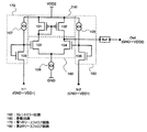
図12(A)(B)に、通常広く用いられているレベルシフタの回路図を示す。なお、本明細書中、各電源電位をVDD#(#は数字)およびGNDとして表記する。ここではVDD1、VDD2、VDD3、VDD4を用い、その大小関係はVDD4<VDD3<GND<VDD1<VDD2とする。また、簡単のため、GND=0[V]に固定する。
【0006】
図12(A)に示したレベルシフタは、GND〜VDD1の電圧振幅を有する入力信号に対し、GND〜VDD2の電圧振幅を有する出力信号を得るものである。つまり低電位側を固定して、高電位側の電位を変換して振幅変換を行う。このレベルシフタの構成は以下のようになっている。第1のP型TFT1201のソース領域と、第2のP型TFT1202のソース領域とはともに電源VDD2に接続されている。第1のP型TFT1201のドレイン領域は第3のP型TFT1203のソース領域と接続され、第2のP型TFT1202のドレイン領域は第4のP型TFT1204のソース領域と接続されている。第3のP型TFT1203のドレイン領域は、第1のN型TFT1205のドレイン領域と、第2のP型TFT1202のゲート電極とに接続され、第4のP型TFT1204のドレイン領域は、第2のN型TFT1206のドレイン領域と、第1のP型TFT1201のゲート電極とに接続されている。第1のN型TFT1205のソース領域と、第2のN型TFT1206のソース領域とはともにGND(=0[V])に接続されている。また、入力信号(In)は、第3のP型TFT1203のゲート電極と、第1のN型TFT1205のゲート電極とに入力され、入力信号の反転信号(Inb)は、第4のP型TFT1204のゲート電極と、第2のN型TFT1206のゲート電極とに入力されている。出力信号(Out)は、第4のP型TFT1204のドレイン領域から取り出される。ここで、第3のP型TFT1203のドレイン領域から、出力信号の反転信号(Outb)を取り出すことも出来る。
【0007】
なお、TFTの導電形式にはN型とP型とがあるが、本明細書中、特にその極性を限定しない場合においては、第1の導電形式、第2の導電形式と記述する。例えば、第1の導電形式と記したTFTがN型である場合には、第2の導電形式とはP型を指し、逆に第1の導電形式と記したTFTがP型である場合には、第2の導電形式とはN型を指すものとする。
【0008】
次に、この従来例のレベルシフタの基本的な動作を説明する。入力信号(In)にHi信号が入力されると、N型TFT1205は導通状態となり、P型TFT1203は非導通状態となるので、P型TFT1202のゲート電極には電位がGND、すなわちLo信号が入力され、P型TFT1202は導通状態となる。一方、反転入力信号(Inb)はこのときLo信号であるから、N型TFT1206は非導通状態となり、P型TFT1204は導通状態となる。従って、P型TFT1202、1204が共に導通状態となったことになり出力信号(OUT)は、Hi信号が出力され、このときの電位はVDD2となる。なお、P型TFT1201は非導通状態となり、P型TFT1202のゲート電極の電位をLo=GNDに保持することを保証する。
【0009】
入力信号(In)の電位がLo信号の時は、図12(A)に示すレベルシフタが対称構造をとることから上記と同様に理解でき、出力端子(OUT)からはLo信号が出力され、このときの電位はGND、すなわち0[V]となる。
【0010】
このようにして、GND〜VDD1の電圧振幅を有する入力信号は、GND〜VDD2の電圧振幅を有する出力信号に変換される。
【0011】
続いて、図12(B)に示したレベルシフタは、VDD3〜GNDの電圧振幅を有する入力信号に対し、VDD4〜GNDの電圧振幅を有する出力信号を得るものである。つまり高電位側を固定して、低電位側の電位を変換して振幅変換を行う。このレベルシフタの構成は以下のようになっている。第1のN型TFT1211のソース領域と、第2のN型TFT1212のソース領域とはともに電源VDD4に接続されている。第1のN型TFT1211のドレイン領域は第3のN型TFT1213のソース領域と接続され、第2のN型TFT1212のドレイン領域は第4のN型TFT1214のソース領域と接続されている。第3のN型TFT1213のドレイン領域は、第1のP型TFT1215のドレイン領域と、第2のN型TFT1212のゲート電極とに接続され、第4のN型TFT1214のドレイン領域は、第2のP型TFT1216のドレイン領域と、第1のN型TFT1211のゲート電極とに接続されている。第1のP型TFT1215のソース領域と、第2のP型TFT1216のソース領域とはともにGND(=0[V])に接続されている。また、入力信号(In)は、第3のN型TFT1213のゲート電極と、第1のP型TFT1215のゲート電極とに入力され、入力信号の反転信号(Inb)は、第4のN型TFT1214のゲート電極と、第2のP型TFT1216のゲート電極とに入力されている。出力信号(Out)は、第4のN型TFT1214のドレイン領域から取り出される。ここで、第3のN型TFT1213のドレイン領域から、出力信号の反転信号(Outb)を取り出すことも出来る。
【0012】
次に、この従来例のレベルシフタの基本的な動作を説明する。入力信号(In)にLo信号が入力されると、P型TFT1215は導通状態となり、N型TFT1213は非導通状態となるので、N型TFT1212のゲート電極には電位がGND、すなわちHi信号が入力され、N型TFT1212は導通状態となる。一方、反転入力信号(Inb)はこのときHi信号であるから、P型TFT1216は非導通状態となり、N型TFT1214は導通状態となる。従って、P型TFT1212、1214が共に導通状態となったことになり出力信号(OUT)は、Lo信号が出力され、このときの電位はVDD4となる。なお、N型TFT1211は非導通状態となり、N型TFT1212のゲート電極の電位をHi=GNDに保持することを保証する。
【0013】
入力信号(In)の電位がHi信号の時は、図12(B)に示すレベルシフタが対称構造をとることから上記と同様に理解でき、出力端子(OUT)からはHi信号が出力され、このときの電位はGND、すなわち0[V]となる。
【0014】
このようにして、VDD3〜GNDの電圧振幅を有する入力信号は、VDD4〜GNDの電圧振幅を有する出力信号に変換される。
【0015】
【発明が解決しようとする課題】
図12(A)(B)に示したレベルシフタにおける問題点について述べる。なお、ここでは、図12(A)(B)いずれのレベルシフタについても共通の問題点であるので、例としては図12(A)のみを挙げる。最初に述べたように、最近のコントローラLSIにおいては、3.3[V]動作をするものが主流となってきている。故に、図12(A)に示したレベルシフタにおいて、VDD1=3[V]、VDD2=10[V]程度の場合の変換をしようとすると、TFT1203、1204、1205、1206への入力信号の振幅が3[V]であるのに対し、N型TFT1205、1206のしきい値電圧が仮に3[V]であったとしたら、もはや正常動作は望めない。つまり、変換前の電圧振幅が小さくなるに従い、TFTが十分に導通するだけのゲート・ソース間電圧を得にくくなるため、正常動作が困難になるということである。
【0016】
故に、本発明においては、前述のように駆動回路の低電源電圧化に伴い、入力信号の電圧振幅が小さくなった場合にも正常動作を保証出来るような、新規の構造を有するレベルシフタを提供することを課題とする。
【0017】
【課題を解決するための手段】
前述した課題を解決するために、本発明においては以下に説明するような手段を講じた。
【0018】
従来のレベルシフタにおいては、入力信号は図12(A)におけるTFT1203、1204、1205、1206のゲート電極に入力されていたため、TFTのしきい値の絶対値よりも入力信号の電圧振幅が小さくなると、TFTが十分に導通するだけのゲート・ソース間電圧が得られなくなり、正常動作しなくなるという問題点があった。
【0019】
そこで、本発明のレベルシフタにおいては、入力信号の経路を工夫して、入力信号の電圧振幅が小さくなった場合にも、TFTのしきい値の影響を受けにくくする。また、電圧振幅の変換には、カレントミラー回路と差動回路とを組み合わせた差動増幅回路を用いることによって、高い利得を得られるようにする。
【0020】
以下に、本発明のレベルシフタの構成について記載する。
【0021】
請求項1に記載の、本発明のレベルシフタは、
カレントミラー回路と、
前記カレントミラー回路を負荷とする差動回路と、
前記差動回路に電流を供給する電流源と、
第1のソースフォロア回路と、第2のソースフォロア回路とを有するレベルシフタであって、
第1の入力信号が、前記第1のソースフォロア回路に入力され、
前記第1のソースフォロア回路からの第1の出力信号が、前記差動回路に入力され、
第2の入力信号が、前記第2のソースフォロア回路に入力され、
前記第2のソースフォロア回路からの第2の出力信号が、前記差動回路に入力されることを特徴としている。
【0022】
請求項2に記載の、本発明のレベルシフタは、
カレントミラー回路と、
前記カレントミラー回路を負荷とする差動回路と、
前記差動回路に電流を供給する第1の電流源と、
ゲート電極とドレイン領域とを電気的に接続した、第1および第2のトランジスタと、
前記第1および第2のトランジスタに電流を供給する第2および第3の電流源とを有するレベルシフタであって、
第1の入力信号が、前記第1のトランジスタのソース領域に入力され、
前記第1のトランジスタからの第1の出力信号が、前記差動回路に入力され、
第2の入力信号が、前記第2のトランジスタのソース領域に入力され、
前記第2のトランジスタからの第2の出力信号が、前記差動回路に入力されることを特徴としている。
【0023】
請求項3に記載の、本発明のレベルシフタは、
カレントミラー回路と、
前記カレントミラー回路を負荷とする差動回路と、
前記差動回路に電流を供給する第1の電流源と、
ゲート電極とドレイン領域とを電気的に接続した、第1および第2のトランジスタと、
前記第1および第2のトランジスタに電流を供給する第2および第3の電流源とを有するレベルシフタであって、
前記差動回路は、第3のトランジスタと第4のトランジスタとを有し、
前記第1のトランジスタのドレイン領域と、前記第3のトランジスタのゲート電極とが電気的に接続され、
前記第2のトランジスタのドレイン領域と、前記第4のトランジスタのゲート電極とが電気的に接続され、
第1の入力信号が、前記第1のトランジスタのソース領域に入力され、
前記第1のトランジスタからの第1の出力信号が、前記第3のトランジスタのゲート電極に入力され、
第2の入力信号が、前記第2のトランジスタのソース領域に入力され、
前記第2のトランジスタからの第2の出力信号が、前記第4のトランジスタのゲート電極に入力されることを特徴としている。
【0024】
請求項4に記載の、本発明のレベルシフタは、
ゲート電極とドレイン領域とを電気的に接続した、第1導電形式の第1のトランジスタと、
ゲート電極とドレイン領域とを電気的に接続した、第1導電形式の第2のトランジスタと、
第1導電形式の第3のトランジスタと、第1導電形式の第4のトランジスタとを有する差動回路と、
第2導電形式であって、ゲート電極とドレイン領域とを接続した第5のトランジスタと、第2導電形式の第6のトランジスタとを有するカレントミラー回路と、
前記差動回路と第1の電流源とを電気的に接続する、第1導電形式の第7のトランジスタと、
前記第5のトランジスタと第2の電流源とを電気的に接続する、第2導電形式の第8のトランジスタと、
前記第6のトランジスタと第3の電流源とを電気的に接続する、第2導電形式の第9のトランジスタと、
前記第7、第8および第9のトランジスタのゲート電極に電位を供給する電源部とを有するレベルシフタであって、
第1の入力信号が、前記第1のトランジスタのソース領域に入力され、
前記第1のトランジスタからの第1の出力信号が、前記第3のトランジスタのゲート電極に入力され、
第2の入力信号が、前記第2のトランジスタのソース領域に入力され、
前記第2のトランジスタからの第2の出力信号が、前記第4のトランジスタのゲート電極に入力されることを特徴としている。
【0025】
請求項5に記載の、本発明のレベルシフタは、
第1のカレントミラー回路と、第2のカレントミラー回路と、
前記第1および第2のカレントミラー回路に電気的に接続された差動回路と、
前記差動回路に電流を供給する第1の電流源と、
ゲート電極とドレイン領域とを接続した、第1および第2のトランジスタと、
前記第1および第2のトランジスタに電流を供給する第2および第3の電流源とを有するレベルシフタであって、
第1の入力信号が、前記第1のトランジスタのソース領域に入力され、
前記第1のトランジスタからの第1の出力信号が、前記差動回路に入力され、
第2の入力信号が、前記第2のトランジスタのソース領域に入力され、
前記第2のトランジスタからの第2の出力信号が、前記差動回路に入力されることを特徴としている。
【0026】
請求項6に記載の、本発明のレベルシフタは、
第1のカレントミラー回路と、第2のカレントミラー回路と、
前記第1および第2のカレントミラー回路に電気的に接続された差動回路と、
前記差動回路に電流を供給する第1の電流源と、
ゲート電極とドレイン領域とを電気的に接続した、第1および第2のトランジスタと、
前記第1および第2のトランジスタに電流を供給する第2および第3の電流源とを有するレベルシフタであって、
前記差動回路は、第3のトランジスタと第4のトランジスタとを有し、
前記第1のトランジスタのドレイン領域と、前記第3のトランジスタのゲート電極とが電気的に接続され、
前記第2のトランジスタのドレイン領域と、前記第4のトランジスタのゲート電極とが電気的に接続され、
第1の入力信号が、前記第1のトランジスタのソース領域に入力され、
前記第1のトランジスタからの第1の出力信号が、前記第3のトランジスタのゲート電極に入力され、
第2の入力信号が、前記第2のトランジスタのソース領域に入力され、
前記第2のトランジスタからの第2の出力信号が、前記第4のトランジスタのゲート電極に入力されることを特徴としている。
【0027】
請求項7に記載の、本発明のレベルシフタは、
カレントミラー回路と、
前記カレントミラー回路を負荷とする差動回路と、
前記差動回路に電流を供給する第1の電流源と、
第1のソースフォロア回路と、第2のソースフォロア回路と、
リセット用トランジスタとを有するレベルシフタであって、
第1の入力信号が、前記第1のソースフォロア回路に入力され、
前記第1のソースフォロア回路からの第1の出力信号が、前記差動回路に入力され、
第2の入力信号が、前記第2のソースフォロア回路に入力され、
前記第2のソースフォロア回路からの第2の出力信号が、前記差動回路に入力され、
入力信号の電圧振幅の変換を行わない期間においては、前記リセット用トランジスタにリセット信号を入力することにより、前記電流源において電流の供給が遮断されることを特徴としている。
【0028】
請求項8に記載の、本発明のレベルシフタは、
カレントミラー回路と、
前記カレントミラー回路を負荷とする差動回路と、
前記差動回路に電流を供給する第1の電流源と、
ゲート電極とドレイン領域とを電気的に接続した、第1および第2のトランジスタと、
前記第1および第2のトランジスタに電流を供給する第2および第3の電流源とを有するレベルシフタであって、
第1の入力信号が、前記第1のトランジスタのソース領域に入力され、
前記第1のトランジスタからの第1の出力信号が、前記差動回路に入力され、
第2の入力信号が、前記第2のトランジスタのソース領域に入力され、
前記第2のトランジスタからの第2の出力信号が、前記差動回路に入力され、
電圧振幅の変換を行わない期間においては、前記電流源からの電流供給を遮断することを特徴としている。
【0029】
請求項9に記載の、本発明のレベルシフタは、
ゲート電極とドレイン領域とを接続した、第1導電形式の第1のトランジスタと、
ゲート電極とドレイン領域とを接続した、第1導電形式の第2のトランジスタと、
第1導電形式の第3のトランジスタと、第1導電形式の第4のトランジスタとを有する差動回路と、
第2導電形式であって、ゲート電極とドレイン領域とを接続した第5のトランジスタと、第2導電形式の第6のトランジスタとを有するカレントミラー回路と、
前記差動回路と第1の電流源とを接続する、第1導電形式の第7のトランジスタと、
前記第5のトランジスタと第2の電流源とを電気的に接続する、第2導電形式の第8のトランジスタと、
前記第6のトランジスタと第3の電流源とを電気的に接続する、第2導電形式の第9のトランジスタと、
前記第7、第8および第9のトランジスタのゲート電極に電位を供給する電源部と、
第2導電形式の第10のリセット用トランジスタと、
第1導電形式の第11のリセット用トランジスタとを有するレベルシフタであって、
前記第1のトランジスタのドレイン領域と、前記第3のトランジスタのゲート電極とが電気的に接続され、
前記第2のトランジスタのドレイン領域と、前記第4のトランジスタのゲート電極とが電気的に接続され、
前記第10のリセット用トランジスタのソース領域は、前記第7、第8のトランジスタのソース領域と電気的に接続され、ドレイン領域は前記第7、第8のトランジスタのゲート電極と電気的に接続され、
前記第11のリセット用トランジスタのソース領域は、前記第9のトランジスタのソース領域と電気的に接続され、ドレイン領域は前記第9のトランジスタのゲート電極と電気的に接続され、
第1の入力信号が、前記第1のトランジスタのソース領域に入力され、
前記第1のトランジスタからの出力信号が、前記第3のトランジスタのゲート電極に入力され、
第2の入力信号が、前記第2のトランジスタのソース領域に入力され、
前記第2のトランジスタからの出力信号が、前記第4のトランジスタのゲート電極に入力され、
電圧振幅の変換を行わない期間においては、前記第10、第11のリセット用トランジスタのゲート電極にリセット信号を入力し、前記第7、第8、第9のトランジスタを非導通状態とすることによって、電流の供給が遮断されることを特徴としている。
【0030】
請求項10に記載の、本発明のレベルシフタは、
請求項1乃至請求項9記載のレベルシフタにおいて、
前記第1の入力信号は、低電圧振幅の信号であり、前記第2の入力信号は、前記第1の入力信号と逆の位相を有する低電圧振幅の信号であることを特徴としている。
【0031】
請求項11に記載の、本発明のレベルシフタは、
請求項1乃至請求項9に記載のレベルシフタにおいて、
前記第1の入力信号は、低電圧振幅の信号であり、前記第2の入力信号は、前期第1の入力信号の振幅範囲内における、ある一定電位の信号であることを特徴としている。
【0032】
請求項12に記載の、本発明のレベルシフタは、
請求項1乃至請求項11に記載のレベルシフタにおいて、
前記第1及び第2の入力信号の電圧振幅は、5[V]以下であることを特徴としている。
【0033】
【発明の実施の形態】
【0034】
本発明のレベルシフタの回路構成図を図1に示す。ここでは、電源電位にGND(=0[V])、VDD1、VDD2を用い、それらの大小関係は、GND<VDD1<VDD2とする。本発明のレベルシフタは、点線枠150で囲まれたカレントミラー回路と、点線枠160で囲まれた差動回路と、点線枠170で囲まれた第1のソースフォロア回路と、点線枠180で囲まれた第2のソースフォロア回路と、電流源109とを有している。カレントミラー回路150、差動回路160および電流源109により、差動増幅回路が構成され、信号の電圧振幅の変換が行われる。ここで、カレントミラー回路150は、差動増幅回路の利得を大きくするための負荷として用いている。
【0035】
P型TFT101、102のソース領域は、電源VDD2に接続されている。P型TFT101、102のゲート電極は互いに電気的に接続され、P型TFT101のドレイン領域およびN型TFT103のドレイン領域と電気的に接続されている。P型TFT102のドレイン領域は、N型TFT104のドレイン領域と電気的に接続され、このノードより出力(Out)を得る。N型TFT103、104のソース領域は、電流源109と電気的に接続されている。N型TFT105のソース領域には第1の入力信号(In1)が入力され、N型TFT106のソース領域には第2の入力信号(In2)が入力される。N型TFT105のゲート電極とドレイン領域とは、ともに電流源107およびN型TFT103のゲート電極と電気的に接続されている。N型TFT106のゲート電極とドレイン領域とは、ともに電流源108およびN型TFT104のゲート電極と電気的に接続されている。
【0036】
本発明のレベルシフタの基本的な動作を、図1、図2を用いて説明する。まず、第1の入力端子(In1)からは、GND〜VDD1の振幅を有する信号が入力される。差動回路部160には、電流源109より定電流が供給される。一方、第1のソースフォロア回路170および第2のソースフォロア回路180におけるN型TFT105、106は、ともにゲート電極とドレイン領域とが接続されているので、この2つのTFTはいずれも飽和領域で動作する。よって、N型TFT103のゲート電極には、VDD2−第1の入力端子(In1)間の電圧を、抵抗分割した電位が入力される。この電位をV103と表記する。同様に、第2の入力端子(In2)からも信号が入力され、第1の入力信号の場合と同様にして、N型TFT104のゲート電極には、VDD2−第2の入力端子(In2)間の電圧を抵抗分割した電位が入力される。この電位をV104と表記する。
【0037】
V103、V104の電位は、図2(B)に示すようになる。図1中、点線枠150で囲われたカレントミラー回路と、点線枠160で囲われた差動回路とにより構成される差動増幅回路の動作について説明する。差動回路のN型TFT103、104のソース領域は、電流源109に接続されている。よって、この2つのTFTを流れる電流は常に一定である。ここで、第1の入力信号がHi、第2の入力信号がLoである場合、差動回路への入力電位の大小関係は、V103>V104となる。よって、N型TFT103のゲート・ソース間電圧は大きくなり、N型TFT104のゲート・ソース間電圧は小さくなる。したがって、N型TFT103を流れる電流I103は増加し、N型TFT104を流れる電流I104は減少する。このとき、カレントミラー回路によって、P型TFT101、102には、I103に等しい電流が流れる。よって出力端子(Out)には、I103とT104の差分の電流が流れる。
【0038】
第1の入力信号がHi、第2の入力信号がLoであるときは、I103>I104であるから、出力端子は差分の電流によって充電され、電位が上昇する。逆に、第1の入力信号がLo、第2の入力信号がHiであるときは、出力端子の電位は下降する。よって,出力端子からは、図2(C)に示すようなパルスが得られる。その後、出力端子の後でバッファ等を通すことにより、図2(D)に示すような、GND〜VDD2の振幅を有するパルスが得られる。
【0039】
本実施形態においては、入力信号は、第1の入力信号の反転信号を第2の入力信号としているが、この2つの信号の関係はこの限りでなく、図2(B)に示すように、第1の入力信号のタイミングで、N型TFT103および104のゲート電極に印加される電位が大小関係をとれるような信号であれば良い。
【0040】
また、カレントミラー回路150、差動回路160に関しては、動作を説明するため、ある一態様を示したが、回路構成に関しては、特にここに表記した構成のみに限定しない。
【0041】
【実施例】
以下に本発明の実施例について記述する。
【0042】
[実施例1]
図3に、本発明のレベルシフタの一実施例を示す。本実施例の説明に伴って行ったシミュレーションの条件として、電源電位にGND(=0[V])、VDD1(=3[V])、VDD2(=10[V])を用いて説明する。
【0043】
本実施例のレベルシフタは、点線枠300で囲まれた差動増幅回路と、点線枠320で囲まれた第1のソースフォロア回路、点線枠330で囲まれた第2のソースフォロア回路からなるレベルシフタ部と、点線枠350で囲まれた電源部とによって構成される。
【0044】
まず、電源部の構成から説明する。P型TFT310、311のソース領域と、N型TFT313のゲート電極とは、電源VDD2と電気的に接続されている。N型TFT312、313のソース領域は、電源GNDと電気的に接続されている。N型TFT313のドレイン領域は、P型TFT311のドレイン領域と電気的に接続され、さらにP型TFT310、311のゲート電極と電気的に接続されており、レベルシフタ部へと入力される。このノードをαとする。N型TFT312のドレイン領域は、P型TFT310のドレイン領域およびN型TFT312のゲート電極と電気的に接続され、レベルシフタ部へと入力される。このノードをβとする。
【0045】
続いて、レベルシフタ部の構成について説明する。差動増幅回路300において、P型TFT302、303のソース領域は、電源VDD2と電気的に接続されている。P型TFT302、303のゲート電極は互いに電気的に接続され、P型TFT302のドレイン領域およびN型TFT306のドレイン領域と電気的に接続されている。P型TFT303のドレイン領域は、N型TFT307のドレイン領域と電気的に接続され、このノードより、バッファ(Buf.)等を介して出力(Out)を得る。N型TFT306、307のソース領域は、N型TFT309のドレイン領域と電気的に接続され、N型TFT309のソース領域は、電源GNDと電気的に接続されている。N型TFT309のゲート電極には、ノードβにおける電位が入力される。
【0046】
第1のソースフォロア回路320において、P型TFT301のソース領域は電源VDD2と電気的に接続され、ゲート電極には、ノードαにおける電位が入力される。一方、N型TFT305のソース領域より、第1の入力信号(In1)が入力される。N型TFT305のドレイン領域とゲート電極は電気的に接続され、さらにP型TFT301のドレイン領域と電気的に接続される。このノードの電位は、差動増幅回路内のN型TFT306のゲート電極に入力される。
【0047】
第2のソースフォロア回路330において、P型TFT304のソース領域は電源VDD2と電気的に接続され、ゲート電極には、ノードαにおける電位が入力される。一方、N型TFT308のソース領域より、第1の入力信号(In1)が入力される。N型TFT308のドレイン領域とゲート電極は電気的に接続され、さらにP型TFT304のドレイン領域と電気的に接続される。このノードの電位は、差動増幅回路内のN型TFT307のゲート電極に入力される。
【0048】
本発明のレベルシフタの動作を、図3、図4を用いて説明する。図4は、図3で示した回路に関するシミュレーション結果を示している。
【0049】
まず、電源部について説明する。N型TFT313のゲート電極にVDD2が入力されて、導通する。これによってP型TFT310、311のゲート電極にはGNDが入力され、共に導通する。P型TFT310の導通により、N型TFT312のゲート電極にはVDD2が入力され、導通する。図3中、ノードαには、GNDに対してやや高い電位が現れ、ノードβには、VDD2に対してやや低い電位が現れる。説明のため、以後は前者をGND'、後者をVDD2'と表記する。(シミュレーション結果では、GND'=1.8[V]、VDD2'=6.8[V]。)
【0050】
続いて、レベルシフタ部について説明する。N型TFT309のゲート電極に、先の電源部から出力されるVDD2'が入力され、導通する。よってN型TFT306、307のソース領域には電源GNDが入力される。一方、P型TFT301、304のゲート電極には、先の電源部から出力されるGND'が入力され、導通する。N型TFT305のゲート電極とドレイン領域とは接続されており、N型TFT308のゲート電極とドレイン領域とが接続されているので、この2つのTFTはいずれも飽和領域で動作する。よって、N型TFT306のゲート電極には、VDD2−第1の入力信号(In1)間の電圧を、P型TFT301およびN型TFT305の抵抗によって抵抗分割した電位が入力される。この電位をV306と表記する。また、N型TFT307のゲート電極には、VDD2−第2の入力信号(In2)間の電圧を、P型TFT304およびN型TFT308の有する抵抗によって抵抗分割した電位が入力される。この電位をV307と表記する。
【0051】
V306、V307の電位は、図4(B)に示すようになる。点線枠300で囲われた差動増幅回路は、V306−V307間の電位差を増幅して出力する機能を有する。よって、出力端子(Out)からは、図4(C)に示すようなパルスが得られる。その後、出力端子の後でバッファ等を通すことにより、図4(D)に示すような、GND〜VDD2の振幅を有するパルスが得られる。
【0052】
比較のため、図4(C)(D)には、従来のレベルシフタによって振幅変換を行った場合のシミュレーション結果をプロットしている。図4(C)における、レベルシフタ出力が、既に正常な波形を保っていないことがわかる。図4(D)でのバッファ出力を比較すると、電圧振幅は0〜10[V]を達成しているが、本発明のレベルシフタの出力と比較すると、入力信号に対し、大きく遅延しているのがわかる。このように、本発明のレベルシフタは、従来型では正常に行うことの困難な振幅変換を行うことが出来る。
【0053】
また、本実施例にて示した図3の例では、TFT305、308をN型TFTとしているが、これらをP型TFTとし、TFT305、308のゲート電極とドレイン領域とを入力端子(In1またはIn2)に接続し、ソース領域をTFT301、304のドレイン領域および差動回路の入力部に接続しても良い。
【0054】
[実施例2]
実施例1においては、信号の振幅変換は、低電圧側(GND)を固定し、高電圧側をVDD1からVDD2へと変換することによって行っていた。本実施例においては、高電圧側を固定し、低電圧側を変換して信号の振幅変換を行う構成のレベルシフタの例を示す。また、説明の際に用いる電源電位は、ここではGND、VDD3、VDD4を用い、それらの大小関係は、VDD4<VDD3<GNDとする。本実施例の説明に伴って行ったシミュレーションの条件として、電源電位にGND(=0[V])、VDD3(=−3[V])、VDD4(=−10[V])を用いて説明する。
【0055】
図5に、本実施例のレベルシフタの回路構成を示す。図3に示したレベルシフタを構成するTFTの極性を逆にした形であり、電源VDD2が接続されていた所に、電源VDD4が接続されている。また、入力信号の電圧振幅はVDD3〜GNDであり、このレベルシフタによって、その電圧振幅をVDD4〜GNDに変換する。
【0056】
本発明のレベルシフタの動作を、図5、図6を用いて説明する。図6は、図5で示した回路に関するシミュレーション結果を示している。図5中、点線枠550で示される電源部と、差動増幅回路500およびソースフォロア回路520、530を有するレベルシフタ部とに分けて説明する。
【0057】
まず、電源部について説明する。P型TFT513のゲート電極にVDD4が入力されて、導通する。これによってN型TFT510、511のゲート電極にはGNDが入力され、共に導通する。N型TFT510の導通により、P型TFT512のゲート電極にはVDD4が入力され、導通する。図5中、ノードαには、GNDに対してやや低い電位が現れ、ノードβには、VDD4に対してやや高い電位が現れる。説明のため、以後は前者をGND"、後者をVDD4'と表記する。(シミュレーション結果では、GND"=−3.6[V]、VDD4'=−8.1[V]。)
【0058】
続いて、レベルシフタ部について説明する。まず、第3の信号と第4の信号が、それぞれ図5中、In3およびIn4より入力される。一方、P型TFT509のゲート電極に、先の電源部から出力されるVDD4'が入力され、導通する。よってP型TFT506、507のソース領域には、電源GNDが入力される。一方、N型TFT501、504のゲート電極には、先の電源部から出力されるGND"が入力され、導通する。P型TFT505のゲート電極とドレイン領域とは接続されており、P型TFT508のゲート電極とドレイン領域とが接続されているので、この2つのTFTはいずれも飽和領域で動作する。よって、P型TFT506のゲート電極には、VDD4−第3の入力信号(In3)間の電圧を、N型TFT501およびP型TFT505の抵抗によって抵抗分割した電位が入力される。この電位をV506と表記する。また、P型TFT507のゲート電極には、VDD4−第4の入力信号(In4)間の電圧を、N型TFT504およびP型TFT508の有する抵抗によって抵抗分割した電位が入力される。この電位をV507と表記する。
【0059】
V506、V507の電位は、図6(B)に示すようになる。点線枠500で囲われた差動増幅回路は、V506−V507間の電位差を増幅して出力する機能を有する。よって、出力端子(Out)からは、図6(C)に示すようなパルスが得られる。その後、出力端子の後でバッファ等を通すことにより、図6(D)に示すような、GND〜VDD4の振幅を有するパルスが得られる。
【0060】
また、本実施例にて示した図5の例では、TFT505、508をP型TFTとしているが、これらをN型TFTとし、TFT505、508のゲート電極とドレイン領域とを入力端子(In3またはIn4)に接続し、ソース領域をTFT501、504のドレイン領域および差動回路の入力部に接続しても良い。
【0061】
[実施例3]
実施例1および実施例2にて示した本発明のレベルシフタは、2入力、1出力型であったが、同様の回路を用いて、1入力、1出力型とすることも出来る。本実施例においては、GND〜VDD1の電圧振幅を有する信号を、GND〜VDD2の電圧振幅を有する信号に変換する、1入力、1出力型レベルシフタを例に挙げて述べる。
【0062】
図7は1入力、1出力型レベルシフタの例である。実施例1にて示したレベルシフタと、回路構成上の相違点はない。唯一、実施例1で第2の信号(In2)が入力されていた端子が、電源Vrefに接続されている点が異なる。ここでは、電源電位にGND(=0[V])、VDD1(=3[V])、VDD2(=10[V])、Vref(=1.5[V])を用いる。ここで、Vrefの電位は、入力信号(In)の振幅の範囲内であることが望ましい。本実施例では、例としてGND(=0[V])とVDD1(=3[V])の中間電位となるようにした。
【0063】
本発明のレベルシフタの動作を、図7、図8を用いて説明する。図8は、図7で示した回路に関するシミュレーション結果を示している。図7中、点線枠750で示される電源部と、差動増幅回路700およびソースフォロア回路720、730を有するレベルシフタ部とに分けて説明する。
【0064】
まず、電源部について説明する。N型TFT713のゲート電極にVDD2(=10[V])が入力されて、導通する。これによってP型TFT710、711のゲート電極にはGND(=0[V])が入力され、共に導通する。P型TFT710の導通により、N型TFT712のゲート電極にはVDD2(=10[V])が入力され、導通する。よって、図5中、ノードαには、GNDに対してやや高い電位が現れ、ノードβには、VDD2に対してやや低い電位が現れる。説明のため、以後は前者をGND'、後者をVDD2'と表記する。(シミュレーション結果では、GND'=1.8[V]、VDD2'=6.8[V]。)
【0065】
続いて、レベルシフタ部について説明する。N型TFT709のゲート電極に、先の電源部から出力されるVDD2'が入力され、導通する。よってN型TFT706、707のソース領域と電源GNDが電気的に接続される。一方、P型TFT701、704のゲート電極には、先の電源部から出力されるGND'が入力され、導通する。N型TFT705のゲート電極とドレイン領域とは接続されており、N型TFT708のゲート電極とドレイン領域とが接続されているので、この2つのTFTはいずれも飽和領域で動作する。よって、N型TFT706のゲート電極には、VDD2−第1の入力信号(In)間の電圧を、P型TFT701およびN型TFT705の抵抗によって抵抗分割した電位が入力される。この電位をV706と表記する。また、N型TFT707のゲート電極には、VDD2−第2の入力信号(Inb)間の電圧を、P型TFT704およびN型TFT708の有する抵抗によって抵抗分割した電位が入力される。この電位をV707と表記する。
【0066】
ここで、V706およびV707の大小関係について考える。まずVDD2(=10[V])−Vref(=1.5[V])間の電圧が一定であることから、V707もまた一定の電位をとる。これに対してV706は、図8(A)(B)に示すように、入力信号(In)の電位がHi(=3[V])の時とLo(=0[V])の時でその電位が変化する。以下に、2つの場合に分けてこれらの大小関係について説明する。
【0067】
(1)入力信号(In)にHiが入力される時
このとき、V706は、VDD2(=10[V])−VDD1(=3[V])間の電圧を、P型TFT701およびN型TFT705の抵抗によって抵抗分割した電位となる。ここで、GND(=0[V])<Vref(=1.5[V])<VDD1(=3[V])であるから、大小関係はV706>V707となる。(図8(B))
【0068】
(2)入力信号(In)にLoが入力される時
このとき、V706は、VDD2(=10[V])−GND(=0[V])間の電圧を、P型TFT701およびN型TFT705の抵抗によって抵抗分割した電位となる。(1)と同様、GND(=0[V])<Vref(=1.5[V])<VDD1(=3[V])であるから、大小関係はV706<V707となる。(図8(B))
【0069】
よって、出力端子(Out)からは、図8(C)に示すようなパルスが得られる。その後、出力端子の後でバッファ等を通すことにより、図8(D)に示すような、GND〜VDD2の振幅を有するパルスが得られる。
【0070】
また、本実施例にて示した図7の例では、TFT705、708をN型TFTとしているが、これらをP型TFTとし、TFT705、708のゲート電極とドレイン領域とを入力端子(In)またはVrefに接続し、ソース領域をTFT701、704のドレイン領域および差動回路の入力部に接続しても良い。
【0071】
[実施例4]
本実施例では、装置の画素部とその周辺に設けられる駆動回路部(ソース信号線駆動回路、ゲート信号線駆動回路)のTFTを同時に作製する方法について説明する。但し、説明を簡単にするために、駆動回路部に関しては基本単位であるCMOS回路を図示することとする。
【0072】
まず、図9(A)に示すように、コーニング社の#7059ガラスや#1737ガラスなどに代表されるバリウムホウケイ酸ガラス、またはアルミノホウケイ酸ガラスなどのガラスから成る基板5001上に酸化シリコン膜、窒化シリコン膜または酸化窒化シリコン膜などの絶縁膜から成る下地膜5002を形成する。例えば、プラズマCVD法でSiH4、NH3、N2Oから作製される酸化窒化シリコン膜5002aを10〜200[nm](好ましくは50〜100[nm])形成し、同様にSiH4、N2Oから作製される酸化窒化水素化シリコン膜5002bを50〜200[nm](好ましくは100〜150[nm])の厚さに積層形成する。本実施例では下地膜5002を2層構造として示したが、前記絶縁膜の単層膜または2層以上積層させた構造として形成しても良い。
【0073】
島状半導体層5003〜5006は、非晶質構造を有する半導体膜をレーザー結晶化法や公知の熱結晶化法を用いて作製した結晶質半導体膜で形成する。この島状半導体層5003〜5006の厚さは25〜80[nm](好ましくは30〜60[nm])の厚さで形成する。結晶質半導体膜の材料に限定はないが、好ましくはシリコンまたはシリコンゲルマニウム(SiGe)合金などで形成すると良い。
【0074】
レーザー結晶化法で結晶質半導体膜を作製するには、パルス発振型または連続発光型のエキシマレーザーやYAGレーザー、YVO4レーザーを用いる。これらのレーザーを用いる場合には、レーザー発振器から放射されたレーザー光を光学系で線状に集光し半導体膜に照射する方法を用いると良い。結晶化の条件は実施者が適宣選択するものであるが、エキシマレーザーを用いる場合はパルス発振周波数30[Hz]とし、レーザーエネルギー密度を100〜400[mJ/cm2](代表的には200〜300[mJ/cm2])とする。また、YAGレーザーを用いる場合にはその第2高調波を用いパルス発振周波数1〜10[kHz]とし、レーザーエネルギー密度を300〜600[mJ/cm2](代表的には350〜500[mJ/cm2])とすると良い。そして幅100〜1000[μm]、例えば400[μm]で線状に集光したレーザー光を基板全面に渡って照射し、この時の線状レーザー光の重ね合わせ率(オーバーラップ率)を80〜98[%]として行う。
【0075】
次いで、島状半導体層5003〜5006を覆うゲート絶縁膜5007を形成する。ゲート絶縁膜5007はプラズマCVD法またはスパッタ法を用い、厚さを40〜150[nm]としてシリコンを含む絶縁膜で形成する。本実施例では、120[nm]の厚さで酸化窒化シリコン膜で形成する。勿論、ゲート絶縁膜はこのような酸化窒化シリコン膜に限定されるものでなく、他のシリコンを含む絶縁膜を単層または積層構造として用いても良い。例えば、酸化シリコン膜を用いる場合には、プラズマCVD法でTEOS(Tetraethyl Orthosilicate)とO2とを混合し、反応圧力40[Pa]、基板温度300〜400[℃]とし、高周波(13.56[MHz])、電力密度0.5〜0.8[W/cm2]で放電させて形成することが出来る。このようにして作製される酸化シリコン膜は、その後400〜500[℃]の熱アニールによりゲート絶縁膜として良好な特性を得ることが出来る。
【0076】
そして、ゲート絶縁膜5007上にゲート電極を形成するための第1の導電膜5008と第2の導電膜5009とを形成する。本実施例では、第1の導電膜5008をTaで50〜100[nm]の厚さに形成し、第2の導電膜5009をWで100〜300[nm]の厚さに形成する。
【0077】
Ta膜はスパッタ法で、TaのターゲットをArでスパッタすることにより形成する。この場合、Arに適量のXeやKrを加えると、Ta膜の内部応力を緩和して膜の剥離を防止することが出来る。また、α相のTa膜の抵抗率は20[μΩcm]程度でありゲート電極に使用することが出来るが、β相のTa膜の抵抗率は180[μΩcm]程度でありゲート電極とするには不向きである。α相のTa膜を形成するために、Taのα相に近い結晶構造をもつ窒化タンタルを10〜50[nm]程度の厚さでTaの下地に形成しておくとα相のTa膜を容易に得ることが出来る。
【0078】
W膜を形成する場合には、Wをターゲットとしたスパッタ法で形成する。その他に6フッ化タングステン(WF6)を用いる熱CVD法で形成することも出来る。いずれにしてもゲート電極として使用するためには低抵抗化を図る必要があり、W膜の抵抗率は20[μΩcm]以下にすることが望ましい。W膜は結晶粒を大きくすることで低抵抗率化を図ることが出来るが、W中に酸素などの不純物元素が多い場合には結晶化が阻害され高抵抗化する。このことより、スパッタ法による場合、純度99.9999[%]のWターゲットを用い、さらに成膜時に気相中からの不純物の混入がないように十分配慮してW膜を形成することにより、抵抗率9〜20[μΩcm]を実現することが出来る。
【0079】
なお、本実施例では、第1の導電膜5008をTa、第2の導電膜5009をWとしたが、特に限定されず、いずれもTa、W、Ti、Mo、Al、Cuなどから選ばれた元素、または前記元素を主成分とする合金材料もしくは化合物材料で形成してもよい。また、リン等の不純物元素をドーピングした多結晶シリコン膜に代表される半導体膜を用いてもよい。本実施例以外の他の組み合わせの一例で望ましいものとしては、第1の導電膜5008を窒化タンタル(TaN)で形成し、第2の導電膜5009をWとする組み合わせ、第1の導電膜5008を窒化タンタル(TaN)で形成し、第2の導電膜5009をAlとする組み合わせ、第1の導電膜5008を窒化タンタル(TaN)で形成し、第2の導電膜5009をCuとする組み合わせ等が挙げられる。
【0080】
次に、レジストによるマスク5010を形成し、電極及び配線を形成するための第1のエッチング処理を行う。本実施例ではICP(Inductively Coupled Plasma:誘導結合型プラズマ)エッチング法を用い、エッチング用ガスにCF4とCl2を混合し、1[Pa]の圧力でコイル型の電極に500[W]のRF(13.56[MHz])電力を投入してプラズマを生成して行う。基板側(試料ステージ)にも100[W]のRF(13.56[MHz])電力を投入し、実質的に負の自己バイアス電圧を印加する。CF4とCl2を混合した場合にはW膜及びTa膜とも同程度にエッチングされる。
【0081】
上記エッチング条件では、レジストによるマスクの形状を適したものとすることにより、基板側に印加するバイアス電圧の効果により第1の導電層及び第2の導電層の端部がテーパー形状となる。テーパー部の角度は15〜45°となる。ゲート絶縁膜上に残渣を残すことなくエッチングするためには、10〜20[%]程度の割合でエッチング時間を増加させると良い。W膜に対する酸化窒化シリコン膜の選択比は2〜4(代表的には3)であるので、オーバーエッチング処理により、酸化窒化シリコン膜が露出した面は20〜50[nm]程度エッチングされることになる。こうして、第1のエッチング処理により第1の導電層と第2の導電層から成る第1の形状の導電層5011〜5016(第1の導電層5011a〜5016aと第2の導電層5011b〜5016b)を形成する。このとき、ゲート絶縁膜5007においては、第1の形状の導電層5011〜5016で覆われない領域は20〜50[nm]程度エッチングされ薄くなった領域が形成される。(図9(A))
【0082】
そして、第1のドーピング処理を行い、N型を付与する不純物元素を添加する。ドーピングの方法はイオンドープ法もしくはイオン注入法で行えば良い。イオンドープ法の条件はドーズ量を1×10¹³〜5×10¹⁴[atoms/cm2]とし、加速電圧を60〜100[keV]として行う。N型を付与する不純物元素として15族に属する元素、典型的にはリン(P)または砒素(As)を用いるが、ここではリン(P)を用いる。この場合、導電層5011〜5016がN型を付与する不純物元素に対するマスクとなり、自己整合的に第1の不純物領域5017〜5020が形成される。第1の不純物領域5017〜5020には1×1020〜1×1021[atoms/cm3]の濃度範囲でN型を付与する不純物元素を添加する。(図9(B))
【0083】
次に、図9(C)に示すように、レジストマスクは除去しないまま、第2のエッチング処理を行う。エッチングガスにCF4とCl2とO2とを用い、W膜を選択的にエッチングする。この時、第2のエッチング処理により第2の形状の導電層5021〜5026(第1の導電層5021a〜5026aと第2の導電層5021b〜5026b)を形成する。このとき、ゲート絶縁膜5007においては、第2の形状の導電層5021〜5026で覆われない領域はさらに20〜50[nm]程度エッチングされ薄くなった領域が形成される。
【0084】
W膜やTa膜のCF4とCl2の混合ガスによるエッチング反応は、生成されるラジカルまたはイオン種と反応生成物の蒸気圧から推測することが出来る。WとTaのフッ化物と塩化物の蒸気圧を比較すると、Wのフッ化物であるWF6が極端に高く、その他のWCl5、TaF5、TaCl5は同程度である。従って、CF4とCl2の混合ガスではW膜及びTa膜共にエッチングされる。しかし、この混合ガスに適量のO2を添加するとCF4とO2が反応してCOとFになり、FラジカルまたはFイオンが多量に発生する。その結果、フッ化物の蒸気圧が高いW膜のエッチング速度が増大する。一方、TaはFが増大しても相対的にエッチング速度の増加は少ない。また、TaはWに比較して酸化されやすいので、O2を添加することでTaの表面が酸化される。Taの酸化物はフッ素や塩素と反応しないためさらにTa膜のエッチング速度は低下する。従って、W膜とTa膜とのエッチング速度に差を作ることが可能となりW膜のエッチング速度をTa膜よりも大きくすることが可能となる。
【0085】
そして、図10(A)に示すように第2のドーピング処理を行う。この場合、第1のドーピング処理よりもドーズ量を下げて高い加速電圧の条件としてN型を付与する不純物元素をドーピングする。例えば、加速電圧を70〜120[keV]とし、1×10¹³[atoms/cm2]のドーズ量で行い、図9(B)で島状半導体層に形成された第1の不純物領域の内側に新たな不純物領域を形成する。ドーピングは、第2の形状の導電層5021〜5026を不純物元素に対するマスクとして用い、第1の導電層5021a〜5026aの下側の領域の半導体層にも不純物元素が添加されるようにドーピングする。こうして、第2の不純物領域5027〜5031が形成される。この第2の不純物領域5027〜5031に添加されたリン(P)の濃度は、第1の導電層5021a〜5026aのテーパー部の膜厚に従って緩やかな濃度勾配を有している。なお、第1の導電層5021a〜5026aのテーパー部と重なる半導体層において、第1の導電層5021a〜5026aのテーパー部の端部から内側に向かって若干、不純物濃度が低くなっているものの、ほぼ同程度の濃度である。
【0086】
続いて、図10(B)に示すように第3のエッチング処理を行う。エッチングガスにCHF6を用い、反応性イオンエッチング法(RIE法)を用いて行う。第3のエッチング処理により、第1の導電層5021a〜5026aのテーパー部を部分的にエッチングして、第1の導電層が半導体層と重なる領域が縮小される。第3のエッチング処理によって、第3の形状の導電層5032〜5037(第1の導電層5032a〜5037aと第2の導電層5032b〜5037b)を形成する。このとき、ゲート絶縁膜5007においては、第3の形状の導電層5032〜5037で覆われない領域はさらに20〜50[nm]程度エッチングされ薄くなった領域が形成される。
【0087】
第3のエッチング処理によって、第2の不純物領域5027〜5031においては、第1の導電層5032a〜5037aと重なる第2の不純物領域5027a〜5031aと、第1の不純物領域と第2の不純物領域との間の第3の不純物領域5027b〜5031bとが形成される。
【0088】
そして、図10(C)に示すように、P型TFTを形成する島状半導体層5004に、第1の導電型とは逆の導電型の第4の不純物領域5039〜5044を形成する。第3の形状の導電層5033bを不純物元素に対するマスクとして用い、自己整合的に不純物領域を形成する。このとき、N型TFTを形成する島状半導体層5003、5005、保持容量部5006および配線部5034はレジストマスク5038で全面を被覆しておく。不純物領域5039〜5044にはそれぞれ異なる濃度でリンが添加されているが、ジボラン(B2H6)を用いたイオンドープ法で形成し、そのいずれの領域においても不純物濃度が2×10²⁰〜2×10²¹[atoms/cm3]となるようにする。
【0089】
以上までの工程でそれぞれの島状半導体層に不純物領域が形成される。島状半導体層と重なる第3の形状の導電層5032、5033、5035、5036がゲート電極として機能する。また、5034は島状のソース信号線として機能する。5037は容量配線として機能する。
【0090】
レジストマスク5038を除去した後、導電型の制御を目的として、それぞれの島状半導体層に添加された不純物元素を活性化する工程を行う。この工程はファーネスアニール炉を用いる熱アニール法で行う。その他に、レーザーアニール法、またはラピッドサーマルアニール法(RTA法)を適用することが出来る。熱アニール法では酸素濃度が1[ppm]以下、好ましくは0.1[ppm]以下の窒素雰囲気中で400〜700[℃]、代表的には500〜600[℃]で行うものであり、本実施例では500[℃]で4時間の熱処理を行う。ただし、第3の形状の導電層5037〜5042に用いた配線材料が熱に弱い場合には、配線等を保護するため層間絶縁膜(シリコンを主成分とする)を形成した後で活性化を行うことが好ましい。
【0091】
さらに、3〜100[%]の水素を含む雰囲気中で、300〜450[℃]で1〜12時間の熱処理を行い、島状半導体層を水素化する工程を行う。この工程は熱的に励起された水素により半導体層のダングリングボンドを終端する工程である。水素化の他の手段として、プラズマ水素化(プラズマにより励起された水素を用いる)を行っても良い。
【0092】
次いで、第1の層間絶縁膜5045は酸化窒化シリコン膜から100〜200[nm]の厚さで形成する。その上に有機絶縁物材料から成る第2の層間絶縁膜5046を形成する。次いで、コンタクトホールを形成するためのエッチング工程を行う。
【0093】
そして、駆動回路部において島状半導体層のソース領域とコンタクトを形成するソース配線5047、5048、ドレイン領域とコンタクトを形成するドレイン配線5049を形成する。また、画素部においては、接続電極5050、画素電極5051、5052を形成する(図11(A))。この接続電極5050により、ソース信号線5034は、画素TFTと電気的な接続が形成される。なお、画素電極5052及び保持容量は隣り合う画素のものである。
【0094】
以上のようにして、N型TFT、P型TFTを有する駆動回路部と、画素TFT、保持容量を有する画素部とを同一基板上に形成することができる。本明細書中ではこのような基板をアクティブマトリクス基板と呼ぶ。
【0095】
本実施例は、ブラックマトリクスを用いることなく、画素電極間の隙間を遮光することができるように、画素電極の端部を信号線や走査線と重なるように配置されている。
【0096】
また、本実施例で示す工程に従えば、アクティブマトリクス基板の作製に必要なフォトマスクの数を5枚(島状半導体層パターン、第1配線パターン(走査線、信号線、容量配線)、Pチャネル領域のマスクパターン、コンタクトホールパターン、第2配線パターン(画素電極、接続電極含む))とすることができる。その結果、工程を短縮し、製造コストの低減及び歩留まりの向上に寄与することができる。
【0097】
続いて、図11(A)の状態のアクティブマトリクス基板を得た後、アクティブマトリクス基板上に配向膜5053を形成しラビング処理を行う。
【0098】
一方、対向基板5054を用意する。対向基板5054にはカラーフィルター層5055〜5057、オーバーコート層5058を形成する。カラーフィルター層はTFTの上方で赤色のカラーフィルター層5055と青色のカラーフィルター層5056とを重ねて形成し遮光膜を兼ねる構成とする。少なくともTFTと、接続電極と画素電極との間を遮光する必要があるため、それらの位置を遮光するように赤色のカラーフィルターと青色のカラーフィルターを重ねて配置することが好ましい。
【0099】
また、接続電極5050に合わせて赤色のカラーフィルター層5055、青色のカラーフィルター層5056、緑色のカラーフィルター層5057とを重ね合わせてスペーサを形成する。各色のカラーフィルターはアクリル樹脂に顔料を混合したもので1〜3[μm]の厚さで形成する。これは感光性材料を用い、マスクを用いて所定のパターンに形成することができる。スペーサの高さはオーバーコート層5058の厚さ1〜4[μm]を考慮することにより2〜7[μm]、好ましくは4〜6[μm]とすることができ、この高さによりアクティブマトリクス基板と対向基板とを貼り合わせた時のギャップを形成する。オーバーコート層5058は光硬化型または熱硬化型の有機樹脂材料で形成し、例えば、ポリイミドやアクリル樹脂などを用いる。
【0100】
スペーサの配置は任意に決定すれば良いが、例えば図11(B)で示すように接続電極上に位置が合うように対向基板5054上に配置すると良い。また、駆動回路部のTFT上にその位置を合わせてスペーサを対向基板5054上に配置してもよい。このスペーサは駆動回路部の全面に渡って配置しても良いし、ソース配線およびドレイン配線を覆うようにして配置しても良い。
【0101】
オーバーコート層5058を形成した後、対向電極5059をパターニング形成し、配向膜5060を形成した後ラビング処理を行う。
【0102】
そして、画素部と駆動回路部が形成されたアクティブマトリクス基板と対向基板とをシール剤5062で貼り合わせる。シール剤5062にはフィラーが混入されていて、このフィラーとスペーサによって均一な間隔を持って2枚の基板が貼り合わせられる。その後、両基板の間に液晶材料5061を注入し、封止剤(図示せず)によって完全に封止する。液晶材料5061には公知の液晶材料を用いれば良い。このようにして図11(B)に示すアクティブマトリクス型液晶表示装置が完成する。
【0103】
なお、上記の行程により作成されるTFTはトップゲート構造であるが、ボトムゲート構造のTFTやその他の構造のTFTに対しても本実施例は容易に適用され得る。
【0104】
また、本実施例にて例示した表示装置は、液晶表示装置であるが、本発明のレベルシフタは、液晶表示装置のみならず、エレクトロルミネッセンス(EL)を用いたEL表示装置の駆動回路においても有効に利用出来る。
【0105】
[実施例5]
図16に、本発明のレベルシフタを用いての表示装置の構成例を示す。絶縁基板1600上に、ソース信号線駆動回路1601、ゲート信号線駆動回路1602、画素部1607が一体形成されている。ソース信号線駆動回路1601は、レベルシフタ1604、シフトレジスタ1605、アナログスイッチ1606等を有している。
【0106】
表示装置の駆動に必要な信号類は、外部のLSIより供給される。最近では、LSI等の低消費電力化により、3.3[V]等で動作するため、入力された信号は、本発明のレベルシフタ1604にて振幅変換がされ、シフトレジスタ等に送られる。
【0107】
なお、図16では図示していないが、画素部に近いバッファ部等の前に、さらに電圧振幅を変換するためにレベルシフタを配置して、さらに1段階電圧振幅の変換手段を設けることで、表示装置内部での低消費電力化をはかることも出来る。
【0108】
また、本実施例にて示した図16の表示装置は、アナログ映像信号を入力する場合の例であるが、本発明のレベルシフタは、デジタル映像信号を入力する表示装置の駆動回路にも適用することが出来る。
【0109】
[実施例6]
本実施例では、差動回路を異なる構成で用いたレベルシフタにより、バッファを必要とせずにGND〜VDD2の振幅を得るための構成について説明する。
【0110】
図17は、本実施例における、本発明のレベルシフタの回路構成例である。TFT1703および1704を有する差動回路1700を有し、TFT1705とTFT1708、またTFT1706とTFT1707とがそれぞれ第1のカレントミラー回路および第2のカレントミラー回路とを構成している。
【0111】
以下に、図17、図18を用いて、各部の動作について説明する。図18に示したシミュレーションに際しての各電源電圧は、実施例1と同様、GND=0[V]、VDD1=3[V]、VDD2=10[V]とした。また、図17中の電流源は、各電源をTFTを介して接続し、それぞれのTFTのゲート電極の電位の制御により、一定電流を確保している。
【0112】
まず、入力端子より、GND〜VDD1の振幅を有する2つの信号(In1、In2)が入力される(図18(A))。TFT1703、1704のゲート電極には、先の入力信号と電源VDD2との間の電位が入力される。この電位は電流源に配置されたTFTおよびTFT1701、1702の各抵抗値によって分割された電位である。このときの、TFT1703および1704のゲート電極における電位をそれぞれV1703、V1704と表記する(図18(B))
【0113】
電流源1740を流れる電流をI1740、TFT1703を流れる電流をI1703、TFT1704を流れる電流をI1704とすると、I1740=I1703+I1704であり、V1703>V1704のとき、I1703>I1704である。よって、TFT1705、TFT1706を流れる電流の値はそのままI1703、I1704となる。さらに、TFT1705、TFT1706を流れる電流が決定されたことにより、TFT1705、TFT1706のゲート電位も決定する。これらをそれぞれV1705、V1706と表記する。TFT1705とTFT1708とが、またTFT1706とTFT1707とがそれぞれカレントミラーを構成しているので、TFT1707、TFT1708のゲート電位もここで決定される。つまり、V1705=V1708、V1706=V1707であり、V1703とV1704との大小関係が前述の通りであるとき、V1705>V1706、したがって、V1707<V1708となる(図18(C))
【0114】
シミュレーション結果においては、V1707、V1708の電位は、図18(C)に示すように、およそ6.5〜9[V]となる。V1707がHi電位のとき、TFT1707は非導通状態となる。よって、TFT1709、TFT1710のゲート電位は下がり、導通しない。このとき、V1708はLo電位となり、導通する。これにより、出力端子には、VDD2が現れる。次に、V1707がLo電位のとき、TFT1707が導通して、TFT1709、TFT1710のゲート電位が上がり、導通する。このとき、V1708はHi電位であるから、TFT1708は導通しない。これにより、出力端子には、GNDが現れる(図18(D))。
【0115】
また、本実施例にて示した図17の例では、TFT1701、1702をN型TFTとしているが、これらをP型TFTとし、TFT1701、1702のゲート電極とドレイン領域とを入力端子(In1またはIn2)に接続し、ソース領域を電流源1720、1730および差動回路の入力部に接続しても良い。
【0116】
[実施例7]
実施形態では、図1に示したように、入力信号は、TFT105、106のソース領域に入力されていた。本実施例においては、信号の入力方法が異なる一例について述べる。
【0117】
図19に、本実施例における回路構成例を示す。図1との相違点は、差動回路と入力信号(In1、In2)との間に配置されたTFTの接続のみである。図1で、それぞれIn1、In2が接続されていたN型TFT105、106は、それぞれ図19におけるP型TFT1901、1902に置換され、入力信号はそれぞれのゲート電極に入力される。
【0118】
以下に、図19に示したレベルシフタの動作について説明する。
【0119】
差動回路内のTFT1903のゲート電極に印加される電圧、つまりγ点における電位について考える。なお、γ点には、VDD2−GND間のいずれかの電位が現れることは前述したとおりである。
【0120】
まず、入力信号(In1)にHiが入力される時、P型TFT1901のゲート電極における電位は3[V]である。このときのP型TFT1901のゲート・ソース間電圧を、VGS1とする。続いて、入力信号(In1)にLoが入力される時、P型TFT1901のゲート電極における電位は0[V]となり、このときのP型TFT1901のゲート・ソース間電圧を、VGS2とする。
【0121】
このとき、|VGS1|<|VGS2|である。各時点におけるTFT1901のON抵抗を、RHi、RLoとすると、Rhi>RLoとなる。TFT1901のON抵抗が低いとき、VDD2−GND間の抵抗分割によってγ点に現れる電位は、よりGNDに引っ張られて低くなる。逆にTFT1901のON抵抗が高いと、γ点に現れる電位は、よりVDD2に引っ張られて高くなる。したがって、P型TFT1903のゲート電極に印加される電圧は、入力信号(In1)と同じ位相をもってある振幅で振動する。差動回路内のTFT1904のゲート電極に印加される電圧、つまりδ点についても、同様の理由により、入力信号(In2)と同じ位相をもってある振幅で振動する。したがって、γ点とδ点の間の電位差を、差動増幅回路によって増幅し、出力する。その後、実施形態、実施例1等の場合と同様にして、0〜VDD2の振幅を有する信号を出力する。
【0122】
[実施例8]
本発明のレベルシフタには、定電流源を用いており、信号の振幅変換を行わない期間においても電流が流れ続けている。そこで本実施例では、そのような期間(具体的には低電圧振幅信号の入力がない帰線期間等)において、低消費電力化を図る方法の一例について述べる。
【0123】
図1に示したように、レベルシフタへの電流供給源は、107、108、109の3箇所である。図20においては、その経路はTFT2001、2002、2003によって制御されており、それらのゲート電極への電位供給は、電源部2050による。よって、レベルシフタへの電流供給を遮断するには、TFT2001、2002、2003を非導通状態とするのが最も簡単な方法である。そこで、図20に示すように、リセット用TFT2004、2005を配置する。本実施例では、リセット用TFT2004にはP型TFTを、リセット用TFT2005にはN型TFTを用いた。TFT2004のソース領域は、電源VDD2に接続されており、ドレイン領域はTFT2001、2002のゲート電極に接続されている。TFT2005のソース領域は、電源GNDに接続されており、ドレイン領域はTFT2003のゲート電極に接続されている。
【0124】
帰線期間等の、レベルシフタが動作しない期間(以後、このような期間をリセット期間と表記する)に、TFT2004、2005のゲート電極へリセット信号(例えばその電圧振幅は0〜VDD2)を入力する。図20に示したような構成でリセット用の回路を配した場合、リセット期間にはHi信号を入力する。これにより、TFT2004、2005が導通し、TFT2001、2002のゲート電極の電位はVDD2に、TFT2003のゲート電極の電位はGNDになり、ともに非導通状態となることにより、各部の電流が遮断される。
【0125】
リセット用TFT2004、2005のチャネル幅は、TFT2001、2002、2003のゲート・ソース間電圧が、十分にそれらのしきい値の絶対値を下回る(具体的には、TFT2004のドレイン領域における電位が十分にVDD2に近づき、TFT2005のドレイン領域における電位が、十分にGNDに近づく)ような電流能力を有するサイズに決定すればよい。
【0126】
[実施例9]
本実施例においては、レベルシフタへの電流供給の遮断を、実施例8とは異なる方法により行う例について述べる。
【0127】
図22に示す回路において、電源部2250におけるTFT2204のゲート電極には、他の実施例にて示した回路ではある一定の電源電位が入力され、常にONの状態となっていた。これに対して本実施例においては、電源制御用パルス(Ctrl.Pulse)が入力される。
【0128】
図22において、TFT2204はN型であるから、電源制御用パルスがHi電位のときにON状態となり、レベルシフタ側のTFT2201〜2203を導通させる。つまり、レベル変換動作の必要な期間にのみ電源制御用パルスを入力し、その期間にのみレベルシフタへの電流供給が行われる。
【0129】
[実施例10]
本発明のレベルシフタを表示装置に適用した際の回路を、実際にTFTを用いて配置した例を図21に示す。図21内に付したTFTの番号301〜309は、それぞれ図3の回路図内に付したTFTの番号301〜309に対応している。
【0130】
図21の例では、電源部が図示されていないが、レベルシフタは、左右方向に複数並列に配置されており、電流源に接続されたTFT301、304、309のゲート電極へ供給する電位は、並列配置されたレベルシフタの外側に有する電源部から、信号線330、340を介して各レベルシフタに供給されている。この電源部は、複数のレベルシフタで共用しても良い。
【0131】
なお、図中、配線アルミニウム・ゲートメタル・半導体層間には、それぞれ絶縁膜を有しており、互いに重なる部分においての短絡はない。コンタクトホールを配した部分で、互いを接続している。
【0132】
本発明のレベルシフタに用いている差動回路およびカレントミラー回路は、その動作の特性上、各々を構成するTFTの特性のばらつきが少ないことが特に重要視される回路である。故に、各回路を構成するTFTは、近接に配置することが望ましい。また、TFT基板の作成工程中、レーザー照射等が含まれる場合にも、図21のように近接配置することにより、照射ムラ等によるTFT特性のばらつきを低減することが出来る。加えて、前述のレーザー照射等は、線状照射が一般的であるため、各TFTを平行に配置することで、さらに前述の照射ムラ等によるTFT特性のばらつきを低減することが出来るため、望ましい。
【0133】
[実施例11]
本発明を適用して作成した駆動回路を用いたアクティブマトリクス型表示装置には様々な用途がある。本実施例では、本発明を適用して作成した駆動回路を用いた表示装置を組み込んだ半導体装置について説明する。
【0134】
このような表示装置には、携帯情報端末(電子手帳、モバイルコンピュータ、携帯電話等)、ビデオカメラ、デジタルカメラ、パーソナルコンピュータ、テレビ、プロジェクタ装置等が挙げられる。それらの一例を図13、図14および図15に示す。
【0135】
図13(A)は携帯電話であり、本体2601、音声出力部2602、音声入力部2603、表示部2604、操作スイッチ2605、アンテナ2606から構成されている。本発明は表示部2604に適用することができる。
【0136】
図13(B)はビデオカメラであり、本体2611、表示部2612、音声入力部2613、操作スイッチ2614、バッテリー2615、受像部2616から成っている。本発明は表示部2612に適用することができる。
【0137】
図13(C)はモバイルコンピュータあるいは携帯型情報端末であり、本体2621、カメラ部2622、受像部2623、操作スイッチ2624、表示部2625で構成されている。本発明は表示部2625に適用することができる。
【0138】
図13(D)はヘッドマウントディスプレイであり、本体2631、表示部2632、アーム部2633で構成される。本発明は表示部2632に適用することができる。
【0139】
図13(E)はテレビであり、本体2641、スピーカー2642、表示部2643、受信装置2644、増幅装置2645等で構成される。本発明は表示部2643に適用することができる。
【0140】
図13(F)は携帯書籍であり、本体2651、表示部2652、記憶媒体2653、操作スイッチ2654、アンテナ2655から構成されており、ミニディスク(MD)やDVD(Digital Versatile Disc)に記憶されたデータや、アンテナで受信したデータを表示するものである。本発明は表示部2652に適用することができる。
【0141】
図14(A)はパーソナルコンピュータであり、本体2701、画像入力部2702、表示部2703、キーボード2704で構成される。本発明は表示部2703に適用することができる。
【0142】
図14(B)はプログラムを記録した記録媒体を用いるプレーヤーであり、本体2711、表示部2712、スピーカー部2713、記録媒体2714、操作スイッチ2715で構成される。なお、この装置は記録媒体としてDVD(Digtial Versatile Disc)、CD等を用い、音楽鑑賞や映画鑑賞やゲームやインターネットを行うことができる。本発明は表示部2612に適用することができる。
【0143】
図14(C)はデジタルカメラであり、本体2721、表示部2722、接眼部2723、操作スイッチ2724、受像部(図示しない)で構成される。本発明は表示部2722に適用することができる。
【0144】
図14(D)は片眼のヘッドマウントディスプレイであり、表示部2731、バンド部2732で構成される。本発明は表示部2731に適用することができる。
【0145】
図15(A)はフロント型プロジェクタであり、投射装置本体2801、表示装置2802、光源2803、光学系2804、スクリーン2805で構成されている。なお、投射装置2801には単版式のものを用いても良いし、R、G、Bの光にそれぞれ対応した三板式のものを用いても良い。本発明は表示装置2802に適用することができる。
【0146】
図15(B)はリア型プロジェクタであり、本体2811、投射装置本体2812、表示装置2813、光源2814、光学系2815、リフレクター2816、スクリーン2817で構成されている。なお、投射装置2813には単版式のものを用いても良いし、R、G、Bの光にそれぞれ対応した三板式のものを用いても良い。本発明は表示装置2813に適用することができる。
【0147】
なお、図15(C)は、図15(A)及び図15(B)中における投射装置本体2801、2812の構造の一例を示した図である。投射装置2801、2812は、光源光学系2821、ミラー2822、2824〜2826、ダイクロイックミラー2823、プリズム2827、表示装置2828、位相差板2829、投射光学系2830で構成される。投射光学系2830は、投射レンズを含む光学系で構成される。本実施例は三板式の例を示したが、特に限定されず、例えば単板式であっても良い。また、図15(C)中において矢印で示した光路に実施者が適宜、光学レンズや、偏光機能を有するフィルムや、位相差を調節するためのフィルム、IRフィルム等の光学系を設けても良い。
【0148】
また、図15(D)は、図15(C)中における光源光学系2821の構造の一例を示した図である。本実施例では、図15(C)中における光源光学系2821は、図15(D)中におけるリフレクター2831、光源2832、レンズアレイ2833、偏光変換素子2834、集光レンズ2835で構成される。なお、図15(D)に示した光源光学系は一例であって特に限定されない。例えば、光源光学系に実施者が適宜、光学レンズや、偏光機能を有するフィルムや、位相差を調節するフィルム、IRフィルム等の光学系を設けても良い。
【発明の効果】
差動増幅回路を有する本発明のレベルシフタによって、入力信号の電圧振幅が小さい場合にも、十分な変換能力を提供することが出来る。これにより、駆動回路の低駆動電圧化が進み、駆動回路と画素部との駆動電圧の差が大きくなるような場合にも、正常に信号の振幅の変換を可能とする。
【0149】
また、本発明のレベルシフタの一態様においては、信号入力について、ゲート電極への直接の入力を避けた構造としており、入力信号の電圧振幅が小さい場合に、TFTのしきい値の影響を受けることを低減しているため、今後の駆動回路の低駆動電圧化に大いに貢献する。
【図面の簡単な説明】
【図1】 本発明の2入力1出力型レベルシフタの回路図。
【図2】 図1に示したレベルシフタの駆動時の各部の電位の模式図。
【図3】 実施例1にて示した本発明の2入力1出力型レベルシフタの回路図。
【図4】 図3に示したレベルシフタの駆動時の各部の電位のシミュレーション結果を示す図。
【図5】 実施例2にて示した本発明の2入力1出力型レベルシフタの回路図。
【図6】 図5に示したレベルシフタの駆動時の各部の電位のシミュレーション結果を示す図。
【図7】 実施例3にて示した本発明の1入力1出力型レベルシフタの回路図。
【図8】 図5に示したレベルシフタの駆動時の各部の電位のシミュレーション結果を示す図。
【図9】 実施例4にて示したアクティブマトリクス基板の作成工程例を示す図。
【図10】 実施例4にて示したアクティブマトリクス基板の作成工程例を示す図。
【図11】 実施例4にて示したアクティブマトリクス基板の作成工程例を示す図。
【図12】 従来の2入力2出力型レベルシフタの回路図。
【図13】 実施例11にて本発明を適用した電子機器の例を示す図。
【図14】 実施例11にて本発明を適用した電子機器の例を示す図。
【図15】 実施例11にて本発明を適用した電子機器の例を示す図。
【図16】 実施例5にて示した、本発明のレベルシフタを用いて同一基板上に形成した表示装置全体の回路の概略図。
【図17】 実施例6にて示した本発明の2入力1出力型レベルシフタの回路図。
【図18】 図17に示したレベルシフタの駆動時の各部の電位のシミュレーション結果を示す図。
【図19】 実施例7にて示した本発明の2入力1出力型レベルシフタの回路図。
【図20】 実施例8にて示した、リセット信号入力を有する本発明のレベルシフタの回路図。
【図21】 実施例10にて示した、各TFTの近接配置を考えた、実設計における本発明のレベルシフタのTFT配置例を示す図。
【図22】 実施例9にて示した、電源制御用信号入力を有する本発明のレベルシフタの回路図。[0001]
BACKGROUND OF THE INVENTION
The present invention relates to a level shifter used for a drive circuit of a display device, and more particularly, to a level shifter used for a drive circuit of a display device using a thin film transistor (hereinafter referred to as TFT) formed on an insulator in the configuration of the drive circuit. About. In this specification, a display device refers to a device used for an LCD (liquid crystal display), an OLED (organic EL display), or the like.
[0002]
[Prior art]
In recent years, semiconductor manufacturing technology has been miniaturized, and along with the accompanying miniaturization of LSI, application to small devices such as portable terminals has also progressed, so that low power consumption has been required. LSIs with low power supply voltage driving such as 3 [V] driving are the mainstream.
[0003]
On the other hand, LCDs (liquid crystal displays), which have been increasing in demand in recent years as applications such as portable terminals and computer monitors, are often driven by signals having a voltage amplitude of 10 [V] to 20 [V]. The drive circuit includes at least a circuit unit that is driven by a corresponding high power supply voltage.
[0004]
Therefore, it is indispensable to connect the controller LSI driven by the low power supply voltage and the liquid crystal drive circuit driven by the high power supply voltage with a level shifter that changes the amplitude voltage width of the signal.
[0005]
FIGS. 12A and 12B are circuit diagrams of level shifters that are ordinarily widely used. Note that in this specification, each power supply potential is expressed as VDD # (# is a number) and GND. Here, VDD1, VDD2, VDD3, and VDD4 are used, and the magnitude relationship is VDD4 <VDD3 <GND <VDD1 <VDD2. For simplicity, GND is fixed to 0 [V].
[0006]
The level shifter shown in FIG. 12A obtains an output signal having a voltage amplitude of GND to VDD2 with respect to an input signal having a voltage amplitude of GND to VDD1. In other words, the low potential side is fixed and the high potential side potential is converted to perform amplitude conversion. The structure of this level shifter is as follows. The source region of the first P-
[0007]
Note that there are N-type and P-type conductivity types of TFTs. In the present specification, when the polarity is not particularly limited, the first conductivity type and the second conductivity type are described. For example, when the TFT described as the first conductivity type is N-type, the second conductivity type indicates the P-type, and conversely, when the TFT described as the first conductivity type is the P-type. The second conductivity type refers to the N type.
[0008]
Next, the basic operation of this conventional level shifter will be described. When the Hi signal is input to the input signal (In), the N-
[0009]
When the potential of the input signal (In) is a Lo signal, the level shifter shown in FIG. 12 (A) has a symmetrical structure, so that it can be understood in the same manner as described above, and the Lo signal is output from the output terminal (OUT). The potential at that time is GND, that is, 0 [V].
[0010]
In this way, an input signal having a voltage amplitude of GND to VDD1 is converted into an output signal having a voltage amplitude of GND to VDD2.
[0011]
Subsequently, the level shifter shown in FIG. 12B obtains an output signal having a voltage amplitude of VDD4 to GND with respect to an input signal having a voltage amplitude of VDD3 to GND. That is, the high potential side is fixed and the potential on the low potential side is converted to perform amplitude conversion. The structure of this level shifter is as follows. The source region of the first N-
[0012]
Next, the basic operation of this conventional level shifter will be described. When the Lo signal is input to the input signal (In), the P-
[0013]
When the potential of the input signal (In) is a Hi signal, the level shifter shown in FIG. 12 (B) has a symmetrical structure, so that it can be understood in the same manner as described above. A Hi signal is output from the output terminal (OUT). The potential at that time is GND, that is, 0 [V].
[0014]
In this way, an input signal having a voltage amplitude of VDD3 to GND is converted into an output signal having a voltage amplitude of VDD4 to GND.
[0015]
[Problems to be solved by the invention]
Problems in the level shifter shown in FIGS. 12A and 12B will be described. Here, since both level shifters in FIGS. 12A and 12B are common problems, only FIG. 12A is given as an example. As described at the beginning, in recent controller LSIs, those operating at 3.3 [V] have become mainstream. Therefore, in the level shifter shown in FIG. 12A, if conversion is performed when VDD1 = 3 [V] and VDD2 = 10 [V], the amplitude of the input signal to the
[0016]
Therefore, the present invention provides a level shifter having a novel structure capable of guaranteeing normal operation even when the voltage amplitude of an input signal is reduced as the power supply voltage of the drive circuit is lowered as described above. This is the issue.
[0017]
[Means for Solving the Problems]
In order to solve the above-described problems, the present invention has taken the following measures.
[0018]
In the conventional level shifter, since the input signal is input to the gate electrodes of the
[0019]
Therefore, in the level shifter of the present invention, the path of the input signal is devised to make it less susceptible to the TFT threshold even when the voltage amplitude of the input signal is reduced. In addition, a high gain can be obtained by converting a voltage amplitude by using a differential amplifier circuit that combines a current mirror circuit and a differential circuit.
[0020]
Below, the structure of the level shifter of this invention is described.
[0021]
The level shifter of the present invention according to
A current mirror circuit;
A differential circuit having the current mirror circuit as a load;
A current source for supplying current to the differential circuit;
A level shifter having a first source follower circuit and a second source follower circuit,
A first input signal is input to the first source follower circuit;
A first output signal from the first source follower circuit is input to the differential circuit;
A second input signal is input to the second source follower circuit;
The second output signal from the second source follower circuit is input to the differential circuit.
[0022]
The level shifter of the present invention according to claim 2
A current mirror circuit;
A differential circuit having the current mirror circuit as a load;
A first current source for supplying current to the differential circuit;
First and second transistors electrically connected to the gate electrode and the drain region;
A level shifter having second and third current sources for supplying current to the first and second transistors,
A first input signal is input to a source region of the first transistor;
A first output signal from the first transistor is input to the differential circuit;
A second input signal is input to a source region of the second transistor;
A second output signal from the second transistor is input to the differential circuit.
[0023]
The level shifter of the present invention according to claim 3
A current mirror circuit;
A differential circuit having the current mirror circuit as a load;
A first current source for supplying current to the differential circuit;
First and second transistors electrically connected to the gate electrode and the drain region;
A level shifter having second and third current sources for supplying current to the first and second transistors,
The differential circuit includes a third transistor and a fourth transistor,
A drain region of the first transistor and a gate electrode of the third transistor are electrically connected;
A drain region of the second transistor is electrically connected to a gate electrode of the fourth transistor;
A first input signal is input to a source region of the first transistor;
A first output signal from the first transistor is input to a gate electrode of the third transistor;
A second input signal is input to a source region of the second transistor;
The second output signal from the second transistor is input to the gate electrode of the fourth transistor.
[0024]
The level shifter of the present invention according to claim 4 is:
A first transistor of the first conductivity type electrically connecting the gate electrode and the drain region;
A second transistor of the first conductivity type in which the gate electrode and the drain region are electrically connected;
A differential circuit having a third transistor of the first conductivity type and a fourth transistor of the first conductivity type;
A current mirror circuit having a second conductivity type and having a fifth transistor in which a gate electrode and a drain region are connected, and a second transistor of a second conductivity type;
A seventh transistor of a first conductivity type electrically connecting the differential circuit and the first current source;
An eighth transistor of the second conductivity type electrically connecting the fifth transistor and a second current source;
A ninth transistor of a second conductivity type electrically connecting the sixth transistor and a third current source;
A level shifter having a power supply for supplying a potential to the gate electrodes of the seventh, eighth and ninth transistors,
A first input signal is input to a source region of the first transistor;
A first output signal from the first transistor is input to a gate electrode of the third transistor;
A second input signal is input to a source region of the second transistor;
The second output signal from the second transistor is input to the gate electrode of the fourth transistor.
[0025]
The level shifter of the present invention according to
A first current mirror circuit; a second current mirror circuit;
A differential circuit electrically connected to the first and second current mirror circuits;
A first current source for supplying current to the differential circuit;
First and second transistors connecting the gate electrode and the drain region;
A level shifter having second and third current sources for supplying current to the first and second transistors,
A first input signal is input to a source region of the first transistor;
A first output signal from the first transistor is input to the differential circuit;
A second input signal is input to a source region of the second transistor;
A second output signal from the second transistor is input to the differential circuit.
[0026]
The level shifter of the present invention according to claim 6
A first current mirror circuit; a second current mirror circuit;
A differential circuit electrically connected to the first and second current mirror circuits;
A first current source for supplying current to the differential circuit;
First and second transistors electrically connected to the gate electrode and the drain region;
A level shifter having second and third current sources for supplying current to the first and second transistors,
The differential circuit includes a third transistor and a fourth transistor,
A drain region of the first transistor and a gate electrode of the third transistor are electrically connected;
A drain region of the second transistor is electrically connected to a gate electrode of the fourth transistor;
A first input signal is input to a source region of the first transistor;
A first output signal from the first transistor is input to a gate electrode of the third transistor;
A second input signal is input to a source region of the second transistor;
The second output signal from the second transistor is input to the gate electrode of the fourth transistor.
[0027]
The level shifter of the present invention according to
A current mirror circuit;
A differential circuit having the current mirror circuit as a load;
A first current source for supplying current to the differential circuit;
A first source follower circuit; a second source follower circuit;
A level shifter having a reset transistor,
A first input signal is input to the first source follower circuit;
A first output signal from the first source follower circuit is input to the differential circuit;
A second input signal is input to the second source follower circuit;
A second output signal from the second source follower circuit is input to the differential circuit;
In a period in which the voltage amplitude of the input signal is not converted, supply of a current to the current source is cut off by inputting a reset signal to the reset transistor.
[0028]
The level shifter of the present invention according to
A current mirror circuit;
A differential circuit having the current mirror circuit as a load;
A first current source for supplying current to the differential circuit;
First and second transistors electrically connected to the gate electrode and the drain region;
A level shifter having second and third current sources for supplying current to the first and second transistors,
A first input signal is input to a source region of the first transistor;
A first output signal from the first transistor is input to the differential circuit;
A second input signal is input to a source region of the second transistor;
A second output signal from the second transistor is input to the differential circuit;
In the period when the voltage amplitude is not converted, the current supply from the current source is cut off.
[0029]
The level shifter of the present invention according to claim 9 comprises:
A first transistor of a first conductivity type connecting a gate electrode and a drain region;
A second transistor of the first conductivity type connecting the gate electrode and the drain region;
A differential circuit having a third transistor of the first conductivity type and a fourth transistor of the first conductivity type;
A current mirror circuit having a second conductivity type and having a fifth transistor in which a gate electrode and a drain region are connected, and a second transistor of a second conductivity type;
A seventh transistor of the first conductivity type connecting the differential circuit and the first current source;
An eighth transistor of the second conductivity type electrically connecting the fifth transistor and a second current source;
A ninth transistor of a second conductivity type electrically connecting the sixth transistor and a third current source;
A power supply for supplying a potential to the gate electrodes of the seventh, eighth and ninth transistors;
A tenth resetting transistor of the second conductivity type;
A level shifter having an eleventh reset transistor of the first conductivity type,
A drain region of the first transistor and a gate electrode of the third transistor are electrically connected;
A drain region of the second transistor is electrically connected to a gate electrode of the fourth transistor;
The source region of the tenth reset transistor is electrically connected to the source regions of the seventh and eighth transistors, and the drain region is electrically connected to the gate electrodes of the seventh and eighth transistors. ,
A source region of the eleventh reset transistor is electrically connected to a source region of the ninth transistor; a drain region is electrically connected to a gate electrode of the ninth transistor;
A first input signal is input to a source region of the first transistor;
The output signal from the first transistor is input to the gate electrode of the third transistor,
A second input signal is input to a source region of the second transistor;
The output signal from the second transistor is input to the gate electrode of the fourth transistor,
In a period in which the voltage amplitude is not converted, a reset signal is input to the gate electrodes of the tenth and eleventh reset transistors, and the seventh, eighth, and ninth transistors are turned off. The current supply is cut off.
[0030]
The level shifter of the present invention according to
The level shifter according to any one of
The first input signal is a low voltage amplitude signal, and the second input signal is a low voltage amplitude signal having a phase opposite to that of the first input signal.
[0031]
The level shifter of the present invention according to claim 11
The level shifter according to any one of
The first input signal is a signal having a low voltage amplitude, and the second input signal is a signal having a certain potential within the amplitude range of the first input signal in the previous period.
[0032]
The level shifter of the present invention according to claim 12
The level shifter according to any one of
The voltage amplitude of the first and second input signals is 5 [V] or less.
[0033]
DETAILED DESCRIPTION OF THE INVENTION
[0034]
A circuit configuration diagram of the level shifter of the present invention is shown in FIG. Here, GND (= 0 [V]), VDD1, and VDD2 are used as power supply potentials, and the magnitude relationship between them is GND <VDD1 <VDD2. The level shifter according to the present invention includes a current mirror circuit surrounded by a dotted
[0035]
The source regions of the P-
[0036]
The basic operation of the level shifter of the present invention will be described with reference to FIGS. First, a signal having an amplitude of GND to VDD1 is input from the first input terminal (In1). A constant current is supplied from the
[0037]
V 103 , V 104 The potential is as shown in FIG. In FIG. 1, the operation of a differential amplifier circuit constituted by a current mirror circuit surrounded by a dotted
[0038]
When the first input signal is Hi and the second input signal is Lo, I 103 > I 104 Therefore, the output terminal is charged by the difference current, and the potential rises. Conversely, when the first input signal is Lo and the second input signal is Hi, the potential of the output terminal decreases. Therefore, a pulse as shown in FIG. 2C is obtained from the output terminal. After that, by passing a buffer or the like after the output terminal, a pulse having an amplitude of GND to VDD2 as shown in FIG.
[0039]
In this embodiment, the input signal uses the inverted signal of the first input signal as the second input signal, but the relationship between the two signals is not limited to this, and as shown in FIG. Any signal may be used as long as the potential applied to the gate electrodes of the N-
[0040]
In addition, for the
[0041]
【Example】
Examples of the present invention will be described below.
[0042]
[Example 1]
FIG. 3 shows an embodiment of the level shifter of the present invention. Description will be made using GND (= 0 [V]), VDD1 (= 3 [V]), and VDD2 (= 10 [V]) as power supply potentials as conditions for simulation performed in conjunction with the description of this embodiment.
[0043]
The level shifter of this embodiment includes a level shifter including a differential amplifier circuit surrounded by a dotted
[0044]
First, the configuration of the power supply unit will be described. The source regions of the P-
[0045]
Next, the configuration of the level shifter unit will be described. In the
[0046]
In the first
[0047]
In the second
[0048]
The operation of the level shifter of the present invention will be described with reference to FIGS. FIG. 4 shows a simulation result related to the circuit shown in FIG.
[0049]
First, the power supply unit will be described. VDD2 is input to the gate electrode of the N-
[0050]
Next, the level shifter unit will be described. VDD2 ′ output from the previous power supply unit is input to the gate electrode of the N-
[0051]
V 306 , V 307 The potential is as shown in FIG. The differential amplifier circuit enclosed by the
[0052]
For comparison, FIGS. 4C and 4D plot the simulation results when amplitude conversion is performed by a conventional level shifter. It can be seen that the level shifter output in FIG. 4C does not already maintain a normal waveform. When the buffer output in FIG. 4 (D) is compared, the voltage amplitude achieves 0 to 10 [V], but when compared with the output of the level shifter of the present invention, it is greatly delayed with respect to the input signal. I understand. Thus, the level shifter of the present invention can perform amplitude conversion that is difficult to perform normally in the conventional type.
[0053]
In the example of FIG. 3 shown in this embodiment, the
[0054]
[Example 2]
In the first embodiment, signal amplitude conversion is performed by fixing the low voltage side (GND) and converting the high voltage side from VDD1 to VDD2. In the present embodiment, an example of a level shifter configured to perform signal amplitude conversion by fixing the high voltage side and converting the low voltage side will be described. In addition, here, GND, VDD3, and VDD4 are used as power supply potentials in the description, and the magnitude relationship between them is VDD4 <VDD3 <GND. As a condition for simulation performed in conjunction with the description of the present embodiment, explanation is made using GND (= 0 [V]), VDD3 (= −3 [V]), VDD4 (= −10 [V]) as the power supply potential. To do.
[0055]
FIG. 5 shows the circuit configuration of the level shifter of this embodiment. The TFTs constituting the level shifter shown in FIG. 3 are reversed in polarity, and the power supply VDD4 is connected to the place where the power supply VDD2 is connected. The voltage amplitude of the input signal is VDD3 to GND, and the voltage amplitude is converted to VDD4 to GND by this level shifter.
[0056]
The operation of the level shifter of the present invention will be described with reference to FIGS. FIG. 6 shows a simulation result related to the circuit shown in FIG. In FIG. 5, the power supply unit indicated by a
[0057]
First, the power supply unit will be described. VDD4 is input to the gate electrode of the P-
[0058]
Next, the level shifter unit will be described. First, the third signal and the fourth signal are input from In3 and In4 in FIG. On the other hand, VDD4 ′ output from the previous power supply unit is input to the gate electrode of the P-
[0059]
V 506 , V 507 Is as shown in FIG. The differential amplifier circuit enclosed by the dotted
[0060]
In the example of FIG. 5 shown in this embodiment, the
[0061]
[Example 3]
Although the level shifter of the present invention shown in
[0062]
FIG. 7 shows an example of a 1-input, 1-output type level shifter. There is no difference in circuit configuration from the level shifter shown in the first embodiment. The only difference is that the terminal to which the second signal (In2) is input in the first embodiment is connected to the power supply Vref. Here, GND (= 0 [V]), VDD1 (= 3 [V]), VDD2 (= 10 [V]), Vref (= 1.5 [V]) are used as the power supply potential. Here, the potential of Vref is preferably within the amplitude range of the input signal (In). In this embodiment, as an example, an intermediate potential between GND (= 0 [V]) and VDD1 (= 3 [V]) is set.
[0063]
The operation of the level shifter of the present invention will be described with reference to FIGS. FIG. 8 shows a simulation result related to the circuit shown in FIG. In FIG. 7, the power supply unit indicated by the dotted
[0064]
First, the power supply unit will be described. VDD2 (= 10 [V]) is input to the gate electrode of the N-
[0065]
Next, the level shifter unit will be described. VDD2 ′ output from the previous power supply unit is input to the gate electrode of the N-
[0066]
Where V 706 And V 707 Think about the size relationship. First, since the voltage between VDD2 (= 10 [V]) − Vref (= 1.5 [V]) is constant, V 707 Also takes a constant potential. On the other hand, V 706 8A and 8B, the potential changes when the potential of the input signal (In) is Hi (= 3 [V]) and Lo (= 0 [V]). . Below, these magnitude relationships will be described in two cases.
[0067]
(1) When Hi is input to the input signal (In)
At this time, V 706 Is a potential obtained by resistance-dividing the voltage between VDD2 (= 10 [V]) − VDD1 (= 3 [V]) by the resistance of the P-
[0068]
(2) When Lo is input to the input signal (In)
At this time, V 706 Is a voltage obtained by dividing the voltage between VDD2 (= 10 [V]) and GND (= 0 [V]) by the resistance of the P-
[0069]
Therefore, a pulse as shown in FIG. 8C is obtained from the output terminal (Out). After that, by passing a buffer or the like after the output terminal, a pulse having an amplitude of GND to VDD2 as shown in FIG. 8D is obtained.
[0070]
In the example of FIG. 7 shown in this embodiment, the
[0071]
[Example 4]
In this embodiment, a method for simultaneously manufacturing TFTs of a pixel portion of a device and a driver circuit portion (a source signal line driver circuit and a gate signal line driver circuit) provided around the pixel portion will be described. However, in order to simplify the description, a CMOS circuit which is a basic unit is illustrated in the drive circuit portion.
[0072]
First, as shown in FIG. 9A, a silicon oxide film is formed on a
[0073]
The island-shaped semiconductor layers 5003 to 5006 are formed using a crystalline semiconductor film in which a semiconductor film having an amorphous structure is formed using a laser crystallization method or a known thermal crystallization method. The island-like semiconductor layers 5003 to 5006 are formed with a thickness of 25 to 80 [nm] (preferably 30 to 60 [nm]). There is no limitation on the material of the crystalline semiconductor film, but the crystalline semiconductor film is preferably formed of silicon or a silicon germanium (SiGe) alloy.
[0074]
In order to fabricate a crystalline semiconductor film by laser crystallization, a pulse oscillation type or continuous emission type excimer laser, YAG laser, YVO Four Use a laser. When these lasers are used, it is preferable to use a method in which laser light emitted from a laser oscillator is linearly collected by an optical system and irradiated onto a semiconductor film. The conditions for crystallization are appropriately selected by the practitioner. When an excimer laser is used, the pulse oscillation frequency is 30 [Hz] and the laser energy density is 100 to 400 [mJ / cm. 2 ] (Typically 200-300 [mJ / cm 2 ]). When a YAG laser is used, the second harmonic is used and the pulse oscillation frequency is set to 1 to 10 [kHz], and the laser energy density is set to 300 to 600 [mJ / cm. 2 ] (Typically 350-500 [mJ / cm 2 ]) Then, a laser beam condensed in a linear shape with a width of 100 to 1000 [μm], for example, 400 [μm] is irradiated over the entire surface of the substrate, and the superposition ratio (overlap ratio) of the linear laser light at this time is 80 Perform as ~ 98 [%].
[0075]
Next, a
[0076]
Then, a first
[0077]
The Ta film is formed by sputtering, and a Ta target is sputtered with Ar. In this case, when an appropriate amount of Xe or Kr is added to Ar, the internal stress of the Ta film can be relieved and peeling of the film can be prevented. The resistivity of the α-phase Ta film is about 20 [μΩcm] and can be used for the gate electrode, but the resistivity of the β-phase Ta film is about 180 [μΩcm] and is used as the gate electrode. It is unsuitable. In order to form an α-phase Ta film, tantalum nitride having a crystal structure close to Ta's α-phase is formed on a Ta base with a thickness of about 10 to 50 nm. It can be easily obtained.
[0078]
When forming a W film, it is formed by sputtering using W as a target. In addition, tungsten hexafluoride (WF 6 It can also be formed by a thermal CVD method using In any case, in order to use as a gate electrode, it is necessary to reduce the resistance, and it is desirable that the resistivity of the W film be 20 [μΩcm] or less. Although the resistivity of the W film can be reduced by increasing the crystal grains, if the impurity element such as oxygen is large in W, the crystallization is hindered and the resistance is increased. From this, in the case of the sputtering method, by using a W target having a purity of 99.9999 [%] and further forming a W film with sufficient consideration so that impurities are not mixed in from the gas phase during film formation, A resistivity of 9 to 20 [μΩcm] can be realized.
[0079]
Note that in this embodiment, the first
[0080]
Next, a resist
[0081]
Under the above etching conditions, by making the shape of the resist mask suitable, the end portions of the first conductive layer and the second conductive layer are tapered due to the effect of the bias voltage applied to the substrate side. The angle of the tapered portion is 15 to 45 °. In order to perform etching without leaving a residue on the gate insulating film, it is preferable to increase the etching time at a rate of about 10 to 20%. Since the selection ratio of the silicon oxynitride film to the W film is 2 to 4 (typically 3), the surface where the silicon oxynitride film is exposed is etched by about 20 to 50 [nm] by the overetching process. become. Thus, the first shape
[0082]
Then, a first doping process is performed, and an impurity element imparting N-type is added. As a doping method, an ion doping method or an ion implantation method may be used. The condition of the ion doping method is a dose of 1 × 10 13 ~ 5x10 14 [atoms / cm 2 The acceleration voltage is set to 60 to 100 [keV]. As an impurity element imparting N-type, an element belonging to Group 15, typically phosphorus (P) or arsenic (As) is used. Here, phosphorus (P) is used. In this case, the
[0083]
Next, as shown in FIG. 9C, a second etching process is performed without removing the resist mask. CF as etching gas Four And Cl 2 And O 2 Then, the W film is selectively etched. At this time, second shape
[0084]
CF of W film and Ta film Four And Cl 2 The etching reaction by the mixed gas can be estimated from the generated radical or ion species and the vapor pressure of the reaction product. Comparing the vapor pressure of fluoride and chloride of W and Ta, WF, which is fluoride of W 6 Is extremely high, other WCl Five , TaF Five , TaCl Five Are comparable. Therefore, CF Four And Cl 2 With this mixed gas, both the W film and the Ta film are etched. However, an appropriate amount of O is added to this mixed gas. 2 When CF is added Four And O 2 Reacts to CO and F, and a large amount of F radicals or F ions are generated. As a result, the etching rate of the W film having a high fluoride vapor pressure is increased. On the other hand, the increase in etching rate of Ta is relatively small even when F increases. Further, since Ta is more easily oxidized than W, O 2 When Ta is added, the surface of Ta is oxidized. Since the Ta oxide does not react with fluorine or chlorine, the etching rate of the Ta film further decreases. Therefore, it is possible to make a difference in the etching rate between the W film and the Ta film, and the etching rate of the W film can be made larger than that of the Ta film.
[0085]
Then, a second doping process is performed as shown in FIG. In this case, the impurity amount imparting N-type is doped as a condition of a high acceleration voltage by lowering the dose than the first doping treatment. For example, the acceleration voltage is set to 70 to 120 [keV] and 1 × 10 13 [atoms / cm 2 A new impurity region is formed inside the first impurity region formed in the island-shaped semiconductor layer in FIG. 9B. Doping is performed using the second shape
[0086]
Subsequently, a third etching process is performed as shown in FIG. CHF as etching gas 6 And using a reactive ion etching method (RIE method). By the third etching treatment, the tapered portions of the first
[0087]
By the third etching process, in the
[0088]
Then, as shown in FIG. 10C,
[0089]
Through the above steps, impurity regions are formed in each island-like semiconductor layer. The third shape
[0090]
After the resist
[0091]
Further, a heat treatment is performed at 300 to 450 [° C.] for 1 to 12 hours in an atmosphere containing 3 to 100 [%] hydrogen to perform a step of hydrogenating the island-shaped semiconductor layer. This step is a step of terminating dangling bonds in the semiconductor layer with thermally excited hydrogen. As another means of hydrogenation, plasma hydrogenation (using hydrogen excited by plasma) may be performed.
[0092]
Next, the first
[0093]
Then,
[0094]
As described above, the driver circuit portion including the N-type TFT and the P-type TFT and the pixel portion including the pixel TFT and the storage capacitor can be formed over the same substrate. In this specification, such a substrate is called an active matrix substrate.
[0095]
In this embodiment, the end portions of the pixel electrodes are arranged so as to overlap the signal lines and the scanning lines so that the gaps between the pixel electrodes can be shielded without using a black matrix.
[0096]
Further, according to the steps shown in this embodiment, the number of photomasks necessary for manufacturing the active matrix substrate is 5 (island semiconductor layer pattern, first wiring pattern (scanning line, signal line, capacitive wiring), P The mask pattern of the channel region, the contact hole pattern, and the second wiring pattern (including the pixel electrode and the connection electrode) can be used. As a result, the process can be shortened, and the manufacturing cost can be reduced and the yield can be improved.
[0097]
Subsequently, after obtaining an active matrix substrate in the state of FIG. 11A, an
[0098]
On the other hand, a
[0099]
In addition, a red
[0100]
The arrangement of the spacers may be arbitrarily determined. For example, as shown in FIG. 11B, the spacers may be arranged on the
[0101]
After the
[0102]
Then, the active matrix substrate on which the pixel portion and the driver circuit portion are formed and the counter substrate are attached to each other with a
[0103]
Although the TFT formed by the above process has a top gate structure, the present embodiment can be easily applied to a TFT having a bottom gate structure and other structures.
[0104]
Although the display device illustrated in this embodiment is a liquid crystal display device, the level shifter of the present invention is effective not only in a liquid crystal display device but also in a drive circuit of an EL display device using electroluminescence (EL). Can be used for
[0105]
[Example 5]
FIG. 16 shows a configuration example of a display device using the level shifter of the present invention. On the insulating substrate 1600, a source signal
[0106]
Signals necessary for driving the display device are supplied from an external LSI. Recently, since operation is performed at 3.3 [V] or the like due to low power consumption of an LSI or the like, an input signal is subjected to amplitude conversion by the level shifter 1604 of the present invention and sent to a shift register or the like.
[0107]
Although not shown in FIG. 16, a level shifter is further disposed in front of the buffer unit or the like close to the pixel unit to further convert the voltage amplitude, and a one-step voltage amplitude converting unit is further provided. It is also possible to reduce power consumption inside the apparatus.
[0108]
The display device of FIG. 16 shown in this embodiment is an example in the case of inputting an analog video signal, but the level shifter of the present invention is also applied to a drive circuit of a display device that inputs a digital video signal. I can do it.
[0109]
[Example 6]
In this embodiment, a configuration for obtaining an amplitude of GND to VDD2 without using a buffer by using a level shifter using a differential circuit in different configurations will be described.
[0110]
FIG. 17 is a circuit configuration example of the level shifter of the present invention in this embodiment. A
[0111]
Hereinafter, the operation of each unit will be described with reference to FIGS. 17 and 18. Each power supply voltage in the simulation shown in FIG. 18 was set to GND = 0 [V], VDD1 = 3 [V], and VDD2 = 10 [V] as in the first embodiment. In the current source in FIG. 17, each power source is connected via a TFT, and a constant current is secured by controlling the potential of the gate electrode of each TFT.
[0112]
First, two signals (In1, In2) having an amplitude of GND to VDD1 are input from the input terminal (FIG. 18A). A potential between the previous input signal and the power supply VDD2 is input to the gate electrodes of the
[0113]
The current flowing through
[0114]
In the simulation results, V 1707 , V 1708 Is approximately 6.5 to 9 [V] as shown in FIG. V 1707 When is at the Hi potential, the
[0115]
In the example of FIG. 17 shown in this embodiment, the
[0116]
[Example 7]
In the embodiment, as illustrated in FIG. 1, the input signal is input to the source regions of the
[0117]
FIG. 19 shows a circuit configuration example in this embodiment. The difference from FIG. 1 is only the connection of the TFTs arranged between the differential circuit and the input signals (In1, In2). In FIG. 1, the N-
[0118]
The operation of the level shifter shown in FIG. 19 will be described below.
[0119]
Consider the voltage applied to the gate electrode of the
[0120]
First, when Hi is input to the input signal (In1), the potential at the gate electrode of the P-
[0121]
At this time, | V GS1 | <| V GS2 | The ON resistance of
[0122]
[Example 8]
The level shifter of the present invention uses a constant current source, and current continues to flow even during a period in which signal amplitude conversion is not performed. In this embodiment, an example of a method for reducing power consumption in such a period (specifically, a blanking period in which no low voltage amplitude signal is input) will be described.
[0123]
As shown in FIG. 1, there are three
[0124]
A reset signal (for example, a voltage amplitude of 0 to VDD2) is input to the gate electrodes of the
[0125]
The channel widths of the
[0126]
[Example 9]
In the present embodiment, an example in which the current supply to the level shifter is interrupted by a method different from that in the eighth embodiment will be described.
[0127]
In the circuit shown in FIG. 22, a constant power supply potential is inputted to the gate electrode of the
[0128]
In FIG. 22, since the
[0129]
[Example 10]
FIG. 21 shows an example in which a circuit when the level shifter of the present invention is applied to a display device is actually arranged using TFTs. The
[0130]
In the example of FIG. 21, the power supply unit is not shown, but a plurality of level shifters are arranged in parallel in the left-right direction, and the potential supplied to the gate electrodes of the
[0131]
In the figure, an insulating film is provided between the wiring aluminum, the gate metal, and the semiconductor layer, and there is no short circuit in the overlapping portion. The contact holes are connected to each other.
[0132]
The differential circuit and the current mirror circuit used in the level shifter of the present invention are circuits that are particularly emphasized in that the characteristics of the TFTs constituting each of the differential circuit and the current mirror circuit are small in terms of operation characteristics. Therefore, it is desirable to arrange the TFTs constituting each circuit close to each other. In addition, even when laser irradiation or the like is included in the TFT substrate manufacturing process, variation in TFT characteristics due to irradiation unevenness or the like can be reduced by arranging them closely as shown in FIG. In addition, since the above-described laser irradiation or the like is generally linear irradiation, it is desirable that each TFT be arranged in parallel to further reduce variation in TFT characteristics due to the above-described irradiation unevenness and the like. .
[0133]
[Example 11]
An active matrix display device using a drive circuit created by applying the present invention has various uses. In this embodiment, a semiconductor device incorporating a display device using a driver circuit created by applying the present invention will be described.
[0134]
Examples of such display devices include portable information terminals (electronic notebooks, mobile computers, mobile phones, etc.), video cameras, digital cameras, personal computers, televisions, projector devices, and the like. Examples of these are shown in FIGS. 13, 14 and 15. FIG.
[0135]
FIG. 13A illustrates a mobile phone, which includes a
[0136]
FIG. 13B illustrates a video camera which includes a main body 2611, a
[0137]
FIG. 13C illustrates a mobile computer or a portable information terminal, which includes a main body 2621, a camera portion 2622, an
[0138]
FIG. 13D illustrates a head mounted display which includes a main body 2631, a
[0139]
FIG. 13E illustrates a television set including a main body 2641, a
[0140]
FIG. 13F illustrates a portable book which includes a main body 2651, a
[0141]
FIG. 14A illustrates a personal computer, which includes a main body 2701, an
[0142]
FIG. 14B shows a player that uses a recording medium in which a program is recorded, and includes a main body 2711, a
[0143]
FIG. 14C illustrates a digital camera which includes a main body 2721, a
[0144]
FIG. 14D illustrates a one-eye head-mounted display which includes a display portion 2731 and a
[0145]
FIG. 15A shows a front projector, which includes a projection apparatus
[0146]
FIG. 15B illustrates a rear projector, which includes a main body 2811, a projection apparatus
[0147]
FIG. 15C is a diagram showing an example of the structure of the projection apparatus
[0148]
FIG. 15D illustrates an example of the structure of the light source optical system 2821 in FIG. In this embodiment, the light source optical system 2821 in FIG. 15C includes the reflector 2831, the light source 2832, the lens array 2833, the polarization conversion element 2834, and the condenser lens 2835 in FIG. Note that the light source optical system illustrated in FIG. 15D is an example and is not particularly limited. For example, the practitioner may appropriately provide an optical system such as an optical lens, a film having a polarization function, a film for adjusting a phase difference, or an IR film in the light source optical system.
【The invention's effect】
The level shifter of the present invention having a differential amplifier circuit can provide sufficient conversion capability even when the voltage amplitude of the input signal is small. Accordingly, even when the drive circuit is lowered in drive voltage and the difference in drive voltage between the drive circuit and the pixel portion becomes large, the signal amplitude can be normally converted.
[0149]
Further, in one aspect of the level shifter of the present invention, the signal input is structured so as to avoid direct input to the gate electrode, and is affected by the threshold value of the TFT when the voltage amplitude of the input signal is small. Therefore, it will greatly contribute to the lower drive voltage of the drive circuit in the future.
[Brief description of the drawings]
FIG. 1 is a circuit diagram of a 2-input 1-output type level shifter according to the present invention.
FIG. 2 is a schematic diagram of the potential of each part when the level shifter shown in FIG. 1 is driven.
3 is a circuit diagram of a two-input one-output type level shifter according to the present invention shown in
4 is a diagram showing a simulation result of potentials at various parts during driving of the level shifter shown in FIG. 3; FIG.
5 is a circuit diagram of a 2-input 1-output type level shifter of the present invention shown in Embodiment 2. FIG.
6 is a diagram showing simulation results of potentials at various parts during driving of the level shifter shown in FIG. 5; FIG.
7 is a circuit diagram of a 1-input 1-output type level shifter of the present invention shown in Embodiment 3. FIG.
FIG. 8 is a diagram showing a simulation result of potentials at various parts when the level shifter shown in FIG. 5 is driven;
FIG. 9 is a diagram illustrating an example of a manufacturing process of an active matrix substrate shown in the fourth embodiment.
FIG. 10 is a diagram showing an example of a manufacturing process of the active matrix substrate shown in the fourth embodiment.
FIG. 11 is a diagram showing an example of a manufacturing process of an active matrix substrate shown in the fourth embodiment.
FIG. 12 is a circuit diagram of a conventional 2-input 2-output type level shifter.
13 is a diagram showing an example of an electronic apparatus to which the present invention is applied in Example 11. FIG.
14 is a diagram showing an example of an electronic apparatus to which the present invention is applied in Example 11. FIG.
15 is a diagram showing an example of an electronic apparatus to which the present invention is applied in Example 11. FIG.
16 is a schematic diagram of a circuit of the entire display device formed on the same substrate using the level shifter of the present invention shown in
FIG. 17 is a circuit diagram of a 2-input 1-output type level shifter of the present invention shown in Embodiment 6.
FIG. 18 is a diagram showing a simulation result of potentials at various parts when the level shifter shown in FIG. 17 is driven;
FIG. 19 is a circuit diagram of a 2-input 1-output type level shifter according to the present invention shown in Example 7.
FIG. 20 is a circuit diagram of a level shifter of the present invention having a reset signal input shown in the eighth embodiment.
FIG. 21 is a diagram showing an example of TFT arrangement of the level shifter of the present invention in an actual design in consideration of the close arrangement of TFTs shown in Example 10;
FIG. 22 is a circuit diagram of a level shifter of the present invention having a power control signal input shown in the ninth embodiment.
Claims (9)
前記カレントミラー回路を負荷とし、第1及び第2の入力端を有する差動回路と、
前記差動回路に電流を供給する第1の電流源と、
第1及び第2のソースフォロア回路と、
リセット回路とを有し、
第1の信号が、前記第1のソースフォロア回路を介して、前記第1の入力端に入力され、
第2の信号が、前記第2のソースフォロア回路を介して、前記第2の入力端に入力され、
前記第1の信号又は前記第2の信号の振幅変換を行わない期間において、前記リセット回路により、前記第1の電流源、前記第1のソースフォロア回路が有する第2の電流源及び前記第2のソースフォロア回路が有する第3の電流源からの電流の供給が遮断されることを特徴とするレベルシフタ。A current mirror circuit;
A differential circuit having the current mirror circuit as a load and having first and second input terminals;
A first current source for supplying current to the differential circuit;
First and second source follower circuits;
A reset circuit,
A first signal is input to the first input terminal via the first source follower circuit;
A second signal is input to the second input terminal via the second source follower circuit;
In a period in which amplitude conversion of the first signal or the second signal is not performed, the reset circuit causes the first current source , the second current source included in the first source follower circuit, and the second A level shifter characterized in that the supply of current from the third current source of the source follower circuit of the first is cut off.
前記カレントミラー回路を負荷とし、第1及び第2の入力端を有する差動回路と、
前記差動回路に電流を供給する第1の電流源と、
第1及び第2のトランジスタと、
第2及び第3の電流源と、
リセット回路とを有し、
前記第1のトランジスタのゲートは、前記第1のトランジスタのソース及びドレインの一方と電気的に接続され、
前記第1のトランジスタのゲートは、前記第1の入力端と電気的に接続され、
前記第2のトランジスタのゲートは、前記第2のトランジスタのソース及びドレインの一方と電気的に接続され、
前記第2のトランジスタのゲートは、前記第2の入力端と電気的に接続され、
前記第2の電流源は、前記第1の入力端と電気的に接続され、
前記第3の電流源は、前記第2の入力端と電気的に接続され、
第1の信号が、前記第1のトランジスタのソース及びドレインの他方に入力され、
第2の信号が、前記第2のトランジスタのソース及びドレインの他方に入力され、
前記第1の信号又は前記第2の信号の振幅変換を行わない期間において、前記リセット回路により、前記第1乃至第3の電流源からの電流の供給が遮断されることを特徴とするレベルシフタ。A current mirror circuit;
A differential circuit having the current mirror circuit as a load and having first and second input terminals;
A first current source for supplying current to the differential circuit;
First and second transistors;
Second and third current sources;
A reset circuit,
A gate of the first transistor is electrically connected to one of a source and a drain of the first transistor;
A gate of the first transistor is electrically connected to the first input terminal;
A gate of the second transistor is electrically connected to one of a source and a drain of the second transistor;
A gate of the second transistor is electrically connected to the second input terminal;
The second current source is electrically connected to the first input terminal,
The third current source is electrically connected to the second input terminal;
A first signal is input to the other of the source and the drain of the first transistor;
A second signal is input to the other of the source and the drain of the second transistor;
A level shifter characterized in that supply of current from the first to third current sources is interrupted by the reset circuit during a period in which amplitude conversion of the first signal or the second signal is not performed.
前記カレントミラー回路を負荷とし、第1及び第2の入力端を有する差動回路と、
前記差動回路に電流を供給する第1の電流源と、
第1及び第2のトランジスタと、
第2及び第3の電流源と、
リセット回路とを有し、
前記第1のトランジスタのソース及びドレインの一方は、前記第1の入力端と電気的に接続され、
前記第2のトランジスタのソース及びドレインの一方は、前記第2の入力端と電気的に接続され、
前記第2の電流源は、前記第1の入力端と電気的に接続され、
前記第3の電流源は、前記第2の入力端と電気的に接続され、
第1の信号が、前記第1のトランジスタのゲートに入力され、
第2の信号が、前記第2のトランジスタのゲートに入力され、
前記第1の信号又は前記第2の信号の振幅変換を行わない期間において、前記リセット回路により、前記第1乃至第3の電流源からの電流の供給が遮断されることを特徴とするレベルシフタ。A current mirror circuit;
A differential circuit having the current mirror circuit as a load and having first and second input terminals;
A first current source for supplying current to the differential circuit;
First and second transistors;
Second and third current sources;
A reset circuit,
One of a source and a drain of the first transistor is electrically connected to the first input terminal;
One of a source and a drain of the second transistor is electrically connected to the second input terminal;
The second current source is electrically connected to the first input terminal,
The third current source is electrically connected to the second input terminal;
A first signal is input to the gate of the first transistor;
A second signal is input to the gate of the second transistor;
A level shifter characterized in that supply of current from the first to third current sources is interrupted by the reset circuit during a period in which amplitude conversion of the first signal or the second signal is not performed.
第3のトランジスタと、第4のトランジスタと、第5のトランジスタと、第6のトランジスタと、を有しA third transistor, a fourth transistor, a fifth transistor, and a sixth transistor;
前記第3のトランジスタのソース及びドレインの一方は、前記第4のトランジスタのソース及びドレインの一方と電気的に接続され、One of a source and a drain of the third transistor is electrically connected to one of a source and a drain of the fourth transistor;
前記第3のトランジスタのゲートは、前記第4のトランジスタのゲートと電気的に接続され、A gate of the third transistor is electrically connected to a gate of the fourth transistor;
前記第4のトランジスタのソース及びドレインの他方は、前記第4のトランジスタのゲートと電気的に接続され、The other of the source and the drain of the fourth transistor is electrically connected to the gate of the fourth transistor;
前記第5のトランジスタのソース及びドレインの一方は、前記第6のトランジスタのソース及びドレインの一方と電気的に接続され、One of a source and a drain of the fifth transistor is electrically connected to one of a source and a drain of the sixth transistor;
前記第5のトランジスタのソース及びドレインの他方は、前記第3のトランジスタのソース及びドレインの他方及び前記第5のトランジスタのゲートと電気的に接続され、The other of the source and the drain of the fifth transistor is electrically connected to the other of the source and the drain of the third transistor and the gate of the fifth transistor;
前記第6のトランジスタのソース及びドレインの他方は、前記第4のトランジスタのソース及びドレインの他方と電気的に接続され、The other of the source and the drain of the sixth transistor is electrically connected to the other of the source and the drain of the fourth transistor;
前記第1の電流源の電流は、前記第5のトランジスタのゲートの電位に応じた値でありThe current of the first current source is a value corresponding to the potential of the gate of the fifth transistor.
前記第2及び第3の電流源の電流は、前記第4のトランジスタのゲートの電位に応じた値であることを特徴とするレベルシフタ。The level shifter characterized in that the currents of the second and third current sources have a value corresponding to the potential of the gate of the fourth transistor.
第3の信号が前記レベルシフタに入力され、A third signal is input to the level shifter;
前記第1乃至第3の電流源からの電流の供給の遮断は、前記第1の信号又は前記第2の信号の振幅変換を行わない期間において前記第3の信号がハイレベル又はロウレベルになることによって行われることを特徴とするレベルシフタ。The interruption of the supply of current from the first to third current sources means that the third signal becomes a high level or a low level in a period in which amplitude conversion of the first signal or the second signal is not performed. Level shifter characterized by being performed by.
前記第1乃至第3の電流源からの電流の供給の遮断は、前記第1の信号又は前記第2の信号の振幅変換を行わない期間において前記第6のトランジスタがオフになることによって行われることを特徴とするレベルシフタ。The supply of current from the first to third current sources is interrupted by turning off the sixth transistor in a period in which amplitude conversion of the first signal or the second signal is not performed. Level shifter characterized by that.
前記第1の信号は、前記レベルシフタに供給される電源電圧よりも小さい振幅を有する信号であり、
前記第2の信号は、前記レベルシフタに供給される電源電圧よりも小さい振幅を有し、前記第1の信号と逆の位相を有する信号であることを特徴とするレベルシフタ。In any one of Claims 1 thru | or 6,
The first signal is a signal having an amplitude smaller than a power supply voltage supplied to the level shifter;
The level shifter, wherein the second signal has a smaller amplitude than a power supply voltage supplied to the level shifter and has a phase opposite to that of the first signal.
前記第1の信号は、前記レベルシフタに供給される電源電圧よりも小さい振幅を有する信号であり、
前記第2の信号は、前記第1の信号の振幅における最小値以上、かつ最大値以下の電位を有する定電位の信号であることを特徴とするレベルシフタ。In any one of Claims 1 thru | or 6,
The first signal is a signal having an amplitude smaller than a power supply voltage supplied to the level shifter;
The level shifter characterized in that the second signal is a constant potential signal having a potential not less than a minimum value and not more than a maximum value in the amplitude of the first signal.
Priority Applications (1)
| Application Number | Priority Date | Filing Date | Title |
|---|---|---|---|
| JP2001187689A JP4748884B2 (en) | 2000-06-27 | 2001-06-21 | Level shifter |
Applications Claiming Priority (4)
| Application Number | Priority Date | Filing Date | Title |
|---|---|---|---|
| JP2000193498 | 2000-06-27 | ||
| JP2000-193498 | 2000-06-27 | ||
| JP2000193498 | 2000-06-27 | ||
| JP2001187689A JP4748884B2 (en) | 2000-06-27 | 2001-06-21 | Level shifter |
Related Child Applications (1)
| Application Number | Title | Priority Date | Filing Date |
|---|---|---|---|
| JP2011102946A Division JP5386536B2 (en) | 2000-06-27 | 2011-05-02 | Semiconductor device and electronic equipment |
Publications (3)
| Publication Number | Publication Date |
|---|---|
| JP2002118458A JP2002118458A (en) | 2002-04-19 |
| JP2002118458A5 JP2002118458A5 (en) | 2008-08-21 |
| JP4748884B2 true JP4748884B2 (en) | 2011-08-17 |
Family
ID=26594809
Family Applications (1)
| Application Number | Title | Priority Date | Filing Date |
|---|---|---|---|
| JP2001187689A Expired - Fee Related JP4748884B2 (en) | 2000-06-27 | 2001-06-21 | Level shifter |
Country Status (1)
| Country | Link |
|---|---|
| JP (1) | JP4748884B2 (en) |
Families Citing this family (9)
| Publication number | Priority date | Publication date | Assignee | Title |
|---|---|---|---|---|
| TWI277057B (en) | 2000-10-23 | 2007-03-21 | Semiconductor Energy Lab | Display device |
| US6927753B2 (en) | 2000-11-07 | 2005-08-09 | Semiconductor Energy Laboratory Co., Ltd. | Display device |
| JP4087229B2 (en) * | 2002-03-11 | 2008-05-21 | 三菱電機株式会社 | Amplitude conversion circuit and semiconductor device using the same |
| CN100380811C (en) * | 2002-12-13 | 2008-04-09 | 株式会社半导体能源研究所 | Semiconductor device and display appliance using the semiconductor device |
| JP4573544B2 (en) * | 2004-03-09 | 2010-11-04 | 三菱電機株式会社 | Display device |
| JP4800781B2 (en) * | 2006-01-31 | 2011-10-26 | セイコーインスツル株式会社 | Voltage level shift circuit and semiconductor integrated circuit |
| US7443202B2 (en) | 2006-06-02 | 2008-10-28 | Semiconductor Energy Laboratory Co., Ltd. | Semiconductor device and electronic apparatus having the same |
| JP2014195241A (en) * | 2013-02-28 | 2014-10-09 | Semiconductor Energy Lab Co Ltd | Semiconductor device |
| CN112860001B (en) * | 2021-01-19 | 2022-04-29 | 烽火通信科技股份有限公司 | Fast current mirror circuit |
Family Cites Families (6)
| Publication number | Priority date | Publication date | Assignee | Title |
|---|---|---|---|---|
| JPH04103215A (en) * | 1990-08-23 | 1992-04-06 | Toshiba Corp | Input circuit for semiconductor integrated circuit |
| JP3144166B2 (en) * | 1992-11-25 | 2001-03-12 | ソニー株式会社 | Low amplitude input level conversion circuit |
| JPH09294062A (en) * | 1996-04-25 | 1997-11-11 | Seiko Epson Corp | Input circuit |
| JPH11214979A (en) * | 1998-01-28 | 1999-08-06 | Hitachi Ltd | Semiconductor integrated circuit |
| JP3174027B2 (en) * | 1998-04-23 | 2001-06-11 | 松下電器産業株式会社 | Signal level conversion circuit |
| JPH11355122A (en) * | 1998-06-09 | 1999-12-24 | Mitsubishi Electric Corp | Input buffer of semiconductor device |
-
2001
- 2001-06-21 JP JP2001187689A patent/JP4748884B2/en not_active Expired - Fee Related
Also Published As
| Publication number | Publication date |
|---|---|
| JP2002118458A (en) | 2002-04-19 |
Similar Documents
| Publication | Publication Date | Title |
|---|---|---|
| JP5386536B2 (en) | Semiconductor device and electronic equipment | |
| JP4416901B2 (en) | Level shifter | |
| JP4397555B2 (en) | Semiconductor devices, electronic equipment | |
| JP3590398B2 (en) | Semiconductor device, display device and electronic equipment | |
| JP4831895B2 (en) | Semiconductor device | |
| JP3483714B2 (en) | Active matrix type liquid crystal display | |
| JP4869516B2 (en) | Semiconductor device | |
| US20010005194A1 (en) | Semiconductor device and driving method thereof | |
| JP4748884B2 (en) | Level shifter | |
| JP2002151698A (en) | Semiconductor device and manufacturing method thereof | |
| JP4083493B2 (en) | Display device and electronic apparatus including the display device | |
| JP4869524B2 (en) | Liquid crystal display | |
| JP4353664B2 (en) | Display device drive circuit, display device, and electronic device | |
| JP5232346B2 (en) | Display device source signal line drive circuit and electronic device | |
| JP2004064528A6 (en) | Semiconductor device |
Legal Events
| Date | Code | Title | Description |
|---|---|---|---|
| A521 | Written amendment |
Free format text: JAPANESE INTERMEDIATE CODE: A523 Effective date: 20080617 |
|
| A621 | Written request for application examination |
Free format text: JAPANESE INTERMEDIATE CODE: A621 Effective date: 20080617 |
|
| A977 | Report on retrieval |
Free format text: JAPANESE INTERMEDIATE CODE: A971007 Effective date: 20110112 |
|
| A131 | Notification of reasons for refusal |
Free format text: JAPANESE INTERMEDIATE CODE: A131 Effective date: 20110301 |
|
| A521 | Written amendment |
Free format text: JAPANESE INTERMEDIATE CODE: A523 Effective date: 20110407 |
|
| A01 | Written decision to grant a patent or to grant a registration (utility model) |
Free format text: JAPANESE INTERMEDIATE CODE: A01 Effective date: 20110510 |
|
| A01 | Written decision to grant a patent or to grant a registration (utility model) |
Free format text: JAPANESE INTERMEDIATE CODE: A01 |
|
| A61 | First payment of annual fees (during grant procedure) |
Free format text: JAPANESE INTERMEDIATE CODE: A61 Effective date: 20110517 |
|
| R150 | Certificate of patent or registration of utility model |
Free format text: JAPANESE INTERMEDIATE CODE: R150 |
|
| FPAY | Renewal fee payment (event date is renewal date of database) |
Free format text: PAYMENT UNTIL: 20140527 Year of fee payment: 3 |
|
| FPAY | Renewal fee payment (event date is renewal date of database) |
Free format text: PAYMENT UNTIL: 20140527 Year of fee payment: 3 |
|
| R250 | Receipt of annual fees |
Free format text: JAPANESE INTERMEDIATE CODE: R250 |
|
| R250 | Receipt of annual fees |
Free format text: JAPANESE INTERMEDIATE CODE: R250 |
|
| R250 | Receipt of annual fees |
Free format text: JAPANESE INTERMEDIATE CODE: R250 |
|
| R250 | Receipt of annual fees |
Free format text: JAPANESE INTERMEDIATE CODE: R250 |
|
| LAPS | Cancellation because of no payment of annual fees |