JP4401022B2 - 半導体装置を製造する方法 - Google Patents
半導体装置を製造する方法 Download PDFInfo
- Publication number
- JP4401022B2 JP4401022B2 JP2000539524A JP2000539524A JP4401022B2 JP 4401022 B2 JP4401022 B2 JP 4401022B2 JP 2000539524 A JP2000539524 A JP 2000539524A JP 2000539524 A JP2000539524 A JP 2000539524A JP 4401022 B2 JP4401022 B2 JP 4401022B2
- Authority
- JP
- Japan
- Prior art keywords
- layer
- heat treatment
- hsq
- conductive
- metal
- Prior art date
- Legal status (The legal status is an assumption and is not a legal conclusion. Google has not performed a legal analysis and makes no representation as to the accuracy of the status listed.)
- Expired - Fee Related
Links
Images


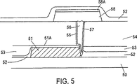
Classifications
-
- H—ELECTRICITY
- H10—SEMICONDUCTOR DEVICES; ELECTRIC SOLID-STATE DEVICES NOT OTHERWISE PROVIDED FOR
- H10P—GENERIC PROCESSES OR APPARATUS FOR THE MANUFACTURE OR TREATMENT OF DEVICES COVERED BY CLASS H10
- H10P95/00—Generic processes or apparatus for manufacture or treatments not covered by the other groups of this subclass
-
- H—ELECTRICITY
- H10—SEMICONDUCTOR DEVICES; ELECTRIC SOLID-STATE DEVICES NOT OTHERWISE PROVIDED FOR
- H10W—GENERIC PACKAGES, INTERCONNECTIONS, CONNECTORS OR OTHER CONSTRUCTIONAL DETAILS OF DEVICES COVERED BY CLASS H10
- H10W20/00—Interconnections in chips, wafers or substrates
- H10W20/01—Manufacture or treatment
- H10W20/071—Manufacture or treatment of dielectric parts thereof
- H10W20/081—Manufacture or treatment of dielectric parts thereof by forming openings in the dielectric parts
-
- H—ELECTRICITY
- H10—SEMICONDUCTOR DEVICES; ELECTRIC SOLID-STATE DEVICES NOT OTHERWISE PROVIDED FOR
- H10W—GENERIC PACKAGES, INTERCONNECTIONS, CONNECTORS OR OTHER CONSTRUCTIONAL DETAILS OF DEVICES COVERED BY CLASS H10
- H10W20/00—Interconnections in chips, wafers or substrates
- H10W20/01—Manufacture or treatment
- H10W20/071—Manufacture or treatment of dielectric parts thereof
- H10W20/093—Manufacture or treatment of dielectric parts thereof by modifying materials of the dielectric parts
- H10W20/096—Manufacture or treatment of dielectric parts thereof by modifying materials of the dielectric parts by contacting with gases, liquids or plasmas
-
- H—ELECTRICITY
- H10—SEMICONDUCTOR DEVICES; ELECTRIC SOLID-STATE DEVICES NOT OTHERWISE PROVIDED FOR
- H10W—GENERIC PACKAGES, INTERCONNECTIONS, CONNECTORS OR OTHER CONSTRUCTIONAL DETAILS OF DEVICES COVERED BY CLASS H10
- H10W20/00—Interconnections in chips, wafers or substrates
- H10W20/01—Manufacture or treatment
- H10W20/071—Manufacture or treatment of dielectric parts thereof
- H10W20/093—Manufacture or treatment of dielectric parts thereof by modifying materials of the dielectric parts
- H10W20/097—Manufacture or treatment of dielectric parts thereof by modifying materials of the dielectric parts by thermally treating
-
- Y—GENERAL TAGGING OF NEW TECHNOLOGICAL DEVELOPMENTS; GENERAL TAGGING OF CROSS-SECTIONAL TECHNOLOGIES SPANNING OVER SEVERAL SECTIONS OF THE IPC; TECHNICAL SUBJECTS COVERED BY FORMER USPC CROSS-REFERENCE ART COLLECTIONS [XRACs] AND DIGESTS
- Y10—TECHNICAL SUBJECTS COVERED BY FORMER USPC
- Y10S—TECHNICAL SUBJECTS COVERED BY FORMER USPC CROSS-REFERENCE ART COLLECTIONS [XRACs] AND DIGESTS
- Y10S438/00—Semiconductor device manufacturing: process
- Y10S438/958—Passivation layer
Landscapes
- Internal Circuitry In Semiconductor Integrated Circuit Devices (AREA)
- Formation Of Insulating Films (AREA)
Applications Claiming Priority (3)
| Application Number | Priority Date | Filing Date | Title |
|---|---|---|---|
| US08/993,124 | 1997-12-18 | ||
| US08/993,124 US6093635A (en) | 1997-12-18 | 1997-12-18 | High integrity borderless vias with HSQ gap filled patterned conductive layers |
| PCT/US1998/026951 WO1999031725A1 (en) | 1997-12-18 | 1998-12-18 | High integrity borderless vias with hsq gap filled patterned conductive layers |
Publications (3)
| Publication Number | Publication Date |
|---|---|
| JP2002509356A JP2002509356A (ja) | 2002-03-26 |
| JP2002509356A5 JP2002509356A5 (https=) | 2006-01-26 |
| JP4401022B2 true JP4401022B2 (ja) | 2010-01-20 |
Family
ID=25539121
Family Applications (1)
| Application Number | Title | Priority Date | Filing Date |
|---|---|---|---|
| JP2000539524A Expired - Fee Related JP4401022B2 (ja) | 1997-12-18 | 1998-12-18 | 半導体装置を製造する方法 |
Country Status (5)
| Country | Link |
|---|---|
| US (1) | US6093635A (https=) |
| EP (1) | EP1040513A1 (https=) |
| JP (1) | JP4401022B2 (https=) |
| KR (1) | KR100572037B1 (https=) |
| WO (1) | WO1999031725A1 (https=) |
Families Citing this family (15)
| Publication number | Priority date | Publication date | Assignee | Title |
|---|---|---|---|---|
| EP0856886B1 (en) * | 1997-01-31 | 2003-06-25 | STMicroelectronics S.r.l. | Process for forming an edge structure to seal integrated electronic devices, and corresponding device |
| JPH11354637A (ja) * | 1998-06-11 | 1999-12-24 | Oki Electric Ind Co Ltd | 配線の接続構造及び配線の接続部の形成方法 |
| US6235453B1 (en) * | 1999-07-07 | 2001-05-22 | Advanced Micro Devices, Inc. | Low-k photoresist removal process |
| US6551943B1 (en) * | 1999-09-02 | 2003-04-22 | Texas Instruments Incorporated | Wet clean of organic silicate glass films |
| US6794298B2 (en) * | 2000-02-04 | 2004-09-21 | Advanced Micro Devices, Inc. | CF4+H2O plasma ashing for reduction of contact/via resistance |
| KR100407998B1 (ko) * | 2001-10-09 | 2003-12-01 | 주식회사 하이닉스반도체 | 금속 배선의 콘택 영역 세정 방법 |
| KR100422905B1 (ko) * | 2001-10-31 | 2004-03-16 | 아남반도체 주식회사 | 반도체 소자 제조 방법 |
| US6645864B1 (en) | 2002-02-05 | 2003-11-11 | Taiwan Semiconductor Manufacturing Company | Physical vapor deposition of an amorphous silicon liner to eliminate resist poisoning |
| US20030162890A1 (en) * | 2002-02-15 | 2003-08-28 | Kalantar Thomas H. | Nanoscale polymerized hydrocarbon particles and methods of making and using such particles |
| US6770566B1 (en) | 2002-03-06 | 2004-08-03 | Cypress Semiconductor Corporation | Methods of forming semiconductor structures, and articles and devices formed thereby |
| US7727892B2 (en) * | 2002-09-25 | 2010-06-01 | Intel Corporation | Method and apparatus for forming metal-metal oxide etch stop/barrier for integrated circuit interconnects |
| DE102004002464B4 (de) * | 2004-01-16 | 2005-12-08 | Infineon Technologies Ag | Verfahren zum Füllen von Kontaktlöchern |
| JP4291811B2 (ja) * | 2005-10-24 | 2009-07-08 | 富士通マイクロエレクトロニクス株式会社 | 半導体装置の製造方法 |
| KR102165264B1 (ko) | 2013-10-10 | 2020-10-13 | 삼성전자 주식회사 | 아연 입자를 함유하는 비전도성 폴리머 막, 비전도성 폴리머 페이스트, 이들을 포함하는 반도체 패키지, 및 반도체 패키지의 제조 방법 |
| KR102165267B1 (ko) | 2013-11-18 | 2020-10-13 | 삼성전자 주식회사 | Tsv 구조를 포함하는 집적회로 소자 및 그 제조 방법 |
Family Cites Families (10)
| Publication number | Priority date | Publication date | Assignee | Title |
|---|---|---|---|---|
| US5174043A (en) * | 1990-11-19 | 1992-12-29 | Taiwan Semiconductor Manufacturing Company | Machine and method for high vacuum controlled ramping curing furnace for sog planarization |
| US5219788A (en) * | 1991-02-25 | 1993-06-15 | Ibm Corporation | Bilayer metallization cap for photolithography |
| TW347149U (en) * | 1993-02-26 | 1998-12-01 | Dow Corning | Integrated circuits protected from the environment by ceramic and barrier metal layers |
| US5432073A (en) * | 1993-09-27 | 1995-07-11 | United Microelectronics Corporation | Method for metal deposition without poison via |
| JP3214186B2 (ja) * | 1993-10-07 | 2001-10-02 | 三菱電機株式会社 | 半導体装置の製造方法 |
| JP2751820B2 (ja) * | 1994-02-28 | 1998-05-18 | 日本電気株式会社 | 半導体装置の製造方法 |
| US5451543A (en) * | 1994-04-25 | 1995-09-19 | Motorola, Inc. | Straight sidewall profile contact opening to underlying interconnect and method for making the same |
| US5413940A (en) * | 1994-10-11 | 1995-05-09 | Taiwan Semiconductor Manufacturing Company | Process of treating SOG layer using end-point detector for outgassing |
| JP3070450B2 (ja) * | 1995-07-14 | 2000-07-31 | ヤマハ株式会社 | 多層配線形成法 |
| EP0810648A3 (en) * | 1996-05-31 | 1997-12-29 | Texas Instruments Incorporated | Improvements in or relating to semiconductor devices |
-
1997
- 1997-12-18 US US08/993,124 patent/US6093635A/en not_active Expired - Lifetime
-
1998
- 1998-12-18 KR KR1020007006809A patent/KR100572037B1/ko not_active Expired - Fee Related
- 1998-12-18 JP JP2000539524A patent/JP4401022B2/ja not_active Expired - Fee Related
- 1998-12-18 WO PCT/US1998/026951 patent/WO1999031725A1/en not_active Ceased
- 1998-12-18 EP EP98963261A patent/EP1040513A1/en not_active Withdrawn
Also Published As
| Publication number | Publication date |
|---|---|
| EP1040513A1 (en) | 2000-10-04 |
| KR20010033345A (ko) | 2001-04-25 |
| JP2002509356A (ja) | 2002-03-26 |
| KR100572037B1 (ko) | 2006-04-18 |
| WO1999031725A1 (en) | 1999-06-24 |
| US6093635A (en) | 2000-07-25 |
Similar Documents
| Publication | Publication Date | Title |
|---|---|---|
| JP4422326B2 (ja) | Hsqで間隙充填されたパターニングされた金属層を備えるボーダレスバイア | |
| US6187672B1 (en) | Interconnect with low dielectric constant insulators for semiconductor integrated circuit manufacturing | |
| KR100288496B1 (ko) | 집적회로구조체의구리오염방지방법 | |
| US6156651A (en) | Metallization method for porous dielectrics | |
| US6297554B1 (en) | Dual damascene interconnect structure with reduced parasitic capacitance | |
| JP4401022B2 (ja) | 半導体装置を製造する方法 | |
| US6841466B1 (en) | Method of selectively making copper using plating technology | |
| US6046104A (en) | Low pressure baked HSQ gap fill layer following barrier layer deposition for high integrity borderless vias | |
| US6417116B2 (en) | Semiconductor device having a multilayer interconnection structure | |
| US6046106A (en) | High density plasma oxide gap filled patterned metal layers with improved electromigration resistance | |
| US5942801A (en) | Borderless vias with HSQ gap filled metal patterns having high etching resistance | |
| US6030891A (en) | Vacuum baked HSQ gap fill layer for high integrity borderless vias | |
| US5880030A (en) | Unlanded via structure and method for making same | |
| US5958798A (en) | Borderless vias without degradation of HSQ gap fill layers | |
| EP0790645A2 (en) | Intermetal dielectric planarization | |
| JP2001284451A (ja) | 二次元波形構造の製造方法 | |
| US6682999B1 (en) | Semiconductor device having multilevel interconnections and method of manufacture thereof | |
| US6524944B1 (en) | Low k ILD process by removable ILD | |
| WO1991010261A1 (en) | Semiconductor interconnect structure utilizing a polyimide insulator | |
| US5888898A (en) | HSQ baking for reduced dielectric constant | |
| US6465343B1 (en) | Method for forming backend interconnect with copper etching and ultra low-k dielectric materials | |
| US6010965A (en) | Method of forming high integrity vias | |
| KR100244713B1 (ko) | 반도체 소자의 제조방법 | |
| KR19980025800A (ko) | 플래너 유전체층 형성 방법 및 다중 레벨 배선 패턴 | |
| KR20060118257A (ko) | 반도체 소자의 제조방법 |
Legal Events
| Date | Code | Title | Description |
|---|---|---|---|
| A521 | Request for written amendment filed |
Free format text: JAPANESE INTERMEDIATE CODE: A523 Effective date: 20051125 |
|
| A621 | Written request for application examination |
Free format text: JAPANESE INTERMEDIATE CODE: A621 Effective date: 20051125 |
|
| A977 | Report on retrieval |
Free format text: JAPANESE INTERMEDIATE CODE: A971007 Effective date: 20080303 |
|
| A131 | Notification of reasons for refusal |
Free format text: JAPANESE INTERMEDIATE CODE: A131 Effective date: 20090512 |
|
| A521 | Request for written amendment filed |
Free format text: JAPANESE INTERMEDIATE CODE: A523 Effective date: 20090810 |
|
| A131 | Notification of reasons for refusal |
Free format text: JAPANESE INTERMEDIATE CODE: A131 Effective date: 20090901 |
|
| A521 | Request for written amendment filed |
Free format text: JAPANESE INTERMEDIATE CODE: A523 Effective date: 20090914 |
|
| TRDD | Decision of grant or rejection written | ||
| A01 | Written decision to grant a patent or to grant a registration (utility model) |
Free format text: JAPANESE INTERMEDIATE CODE: A01 Effective date: 20091013 |
|
| A01 | Written decision to grant a patent or to grant a registration (utility model) |
Free format text: JAPANESE INTERMEDIATE CODE: A01 |
|
| A61 | First payment of annual fees (during grant procedure) |
Free format text: JAPANESE INTERMEDIATE CODE: A61 Effective date: 20091027 |
|
| R150 | Certificate of patent or registration of utility model |
Free format text: JAPANESE INTERMEDIATE CODE: R150 |
|
| FPAY | Renewal fee payment (event date is renewal date of database) |
Free format text: PAYMENT UNTIL: 20121106 Year of fee payment: 3 |
|
| FPAY | Renewal fee payment (event date is renewal date of database) |
Free format text: PAYMENT UNTIL: 20121106 Year of fee payment: 3 |
|
| S111 | Request for change of ownership or part of ownership |
Free format text: JAPANESE INTERMEDIATE CODE: R313113 |
|
| FPAY | Renewal fee payment (event date is renewal date of database) |
Free format text: PAYMENT UNTIL: 20121106 Year of fee payment: 3 |
|
| R350 | Written notification of registration of transfer |
Free format text: JAPANESE INTERMEDIATE CODE: R350 |
|
| FPAY | Renewal fee payment (event date is renewal date of database) |
Free format text: PAYMENT UNTIL: 20121106 Year of fee payment: 3 |
|
| FPAY | Renewal fee payment (event date is renewal date of database) |
Free format text: PAYMENT UNTIL: 20131106 Year of fee payment: 4 |
|
| LAPS | Cancellation because of no payment of annual fees |