JP4378980B2 - Electronic components with control terminals - Google Patents
Electronic components with control terminals Download PDFInfo
- Publication number
- JP4378980B2 JP4378980B2 JP2003068345A JP2003068345A JP4378980B2 JP 4378980 B2 JP4378980 B2 JP 4378980B2 JP 2003068345 A JP2003068345 A JP 2003068345A JP 2003068345 A JP2003068345 A JP 2003068345A JP 4378980 B2 JP4378980 B2 JP 4378980B2
- Authority
- JP
- Japan
- Prior art keywords
- package
- inspection
- electronic component
- terminal
- substrate
- Prior art date
- Legal status (The legal status is an assumption and is not a legal conclusion. Google has not performed a legal analysis and makes no representation as to the accuracy of the status listed.)
- Expired - Fee Related
Links
Images


Classifications
-
- H—ELECTRICITY
- H01—ELECTRIC ELEMENTS
- H01L—SEMICONDUCTOR DEVICES NOT COVERED BY CLASS H10
- H01L2224/00—Indexing scheme for arrangements for connecting or disconnecting semiconductor or solid-state bodies and methods related thereto as covered by H01L24/00
- H01L2224/01—Means for bonding being attached to, or being formed on, the surface to be connected, e.g. chip-to-package, die-attach, "first-level" interconnects; Manufacturing methods related thereto
- H01L2224/10—Bump connectors; Manufacturing methods related thereto
- H01L2224/15—Structure, shape, material or disposition of the bump connectors after the connecting process
- H01L2224/16—Structure, shape, material or disposition of the bump connectors after the connecting process of an individual bump connector
- H01L2224/161—Disposition
- H01L2224/16151—Disposition the bump connector connecting between a semiconductor or solid-state body and an item not being a semiconductor or solid-state body, e.g. chip-to-substrate, chip-to-passive
- H01L2224/16221—Disposition the bump connector connecting between a semiconductor or solid-state body and an item not being a semiconductor or solid-state body, e.g. chip-to-substrate, chip-to-passive the body and the item being stacked
- H01L2224/16225—Disposition the bump connector connecting between a semiconductor or solid-state body and an item not being a semiconductor or solid-state body, e.g. chip-to-substrate, chip-to-passive the body and the item being stacked the item being non-metallic, e.g. insulating substrate with or without metallisation
-
- H—ELECTRICITY
- H01—ELECTRIC ELEMENTS
- H01L—SEMICONDUCTOR DEVICES NOT COVERED BY CLASS H10
- H01L2224/00—Indexing scheme for arrangements for connecting or disconnecting semiconductor or solid-state bodies and methods related thereto as covered by H01L24/00
- H01L2224/01—Means for bonding being attached to, or being formed on, the surface to be connected, e.g. chip-to-package, die-attach, "first-level" interconnects; Manufacturing methods related thereto
- H01L2224/26—Layer connectors, e.g. plate connectors, solder or adhesive layers; Manufacturing methods related thereto
- H01L2224/31—Structure, shape, material or disposition of the layer connectors after the connecting process
- H01L2224/32—Structure, shape, material or disposition of the layer connectors after the connecting process of an individual layer connector
- H01L2224/321—Disposition
- H01L2224/32151—Disposition the layer connector connecting between a semiconductor or solid-state body and an item not being a semiconductor or solid-state body, e.g. chip-to-substrate, chip-to-passive
- H01L2224/32221—Disposition the layer connector connecting between a semiconductor or solid-state body and an item not being a semiconductor or solid-state body, e.g. chip-to-substrate, chip-to-passive the body and the item being stacked
- H01L2224/32225—Disposition the layer connector connecting between a semiconductor or solid-state body and an item not being a semiconductor or solid-state body, e.g. chip-to-substrate, chip-to-passive the body and the item being stacked the item being non-metallic, e.g. insulating substrate with or without metallisation
-
- H—ELECTRICITY
- H01—ELECTRIC ELEMENTS
- H01L—SEMICONDUCTOR DEVICES NOT COVERED BY CLASS H10
- H01L2224/00—Indexing scheme for arrangements for connecting or disconnecting semiconductor or solid-state bodies and methods related thereto as covered by H01L24/00
- H01L2224/01—Means for bonding being attached to, or being formed on, the surface to be connected, e.g. chip-to-package, die-attach, "first-level" interconnects; Manufacturing methods related thereto
- H01L2224/42—Wire connectors; Manufacturing methods related thereto
- H01L2224/44—Structure, shape, material or disposition of the wire connectors prior to the connecting process
- H01L2224/45—Structure, shape, material or disposition of the wire connectors prior to the connecting process of an individual wire connector
- H01L2224/45001—Core members of the connector
- H01L2224/45099—Material
- H01L2224/451—Material with a principal constituent of the material being a metal or a metalloid, e.g. boron (B), silicon (Si), germanium (Ge), arsenic (As), antimony (Sb), tellurium (Te) and polonium (Po), and alloys thereof
- H01L2224/45138—Material with a principal constituent of the material being a metal or a metalloid, e.g. boron (B), silicon (Si), germanium (Ge), arsenic (As), antimony (Sb), tellurium (Te) and polonium (Po), and alloys thereof the principal constituent melting at a temperature of greater than or equal to 950°C and less than 1550°C
- H01L2224/45144—Gold (Au) as principal constituent
-
- H—ELECTRICITY
- H01—ELECTRIC ELEMENTS
- H01L—SEMICONDUCTOR DEVICES NOT COVERED BY CLASS H10
- H01L2224/00—Indexing scheme for arrangements for connecting or disconnecting semiconductor or solid-state bodies and methods related thereto as covered by H01L24/00
- H01L2224/73—Means for bonding being of different types provided for in two or more of groups H01L2224/10, H01L2224/18, H01L2224/26, H01L2224/34, H01L2224/42, H01L2224/50, H01L2224/63, H01L2224/71
- H01L2224/732—Location after the connecting process
- H01L2224/73201—Location after the connecting process on the same surface
- H01L2224/73203—Bump and layer connectors
- H01L2224/73204—Bump and layer connectors the bump connector being embedded into the layer connector
Landscapes
- Testing Electric Properties And Detecting Electric Faults (AREA)
- Tests Of Electronic Circuits (AREA)
- Oscillators With Electromechanical Resonators (AREA)
- Piezo-Electric Or Mechanical Vibrators, Or Delay Or Filter Circuits (AREA)
Description
【0001】
【発明の属する技術分野】
本発明は、圧電振動片と集積回路等の複数の部品をパッケージに内蔵した圧電デバイス等の電子部品であって、パッケージ外面に内蔵部品の制御端子を備えた制御端子付き電子部品の改良と、この電子部品を利用した携帯電話装置に関するものである。
【0002】
【従来の技術】
従来、例えば、圧電材料や、合成樹脂により形成したパッケージ内に、集積回路等の電子部品(以下、「内蔵部品」という)を収容して、所定の基板上に面実装されるパッケージ型の電子部品には、例えば、図48に示すようなものが使用されている。
図48において、電子部品1は、内部に図示しない空間を有するパッケージ2を備えている。パッケージ2の内部空間には、図示しない内蔵部品が収容されており、この例では、例えば、圧電振動片と、この圧電振動片に接続された集積回路が内蔵されている。このパッケージ2には、上記内蔵部品を収容した後で、パッケージ2の上方開口を、蓋体3で封止することで、圧電発振器を形成している。
【0003】
このような電子部品1では、面実装を実現するために、パッケージ2の底面には、実装基板(図示せず)の所定のランド上に半田付けにより接続することで、実装基板を介して、内蔵部品に駆動電圧を供給したり、内蔵備品から送られる信号を出力するための実装端子4,4,4,4が形成されている。
また、パッケージ2には、実装端子4,4,4,4とは別に、外部から検査用のプローブまたはピン等を当てて、集積回路等の内蔵部品の動作制御及び/または動作確認を行うために、制御端子5,5,5,5が設けられている。
これにより、電子部品1においては、実装端子4,4,4,4に、検査治具の一部である給電または、信号出力用のピン6,6,6,6等を用いて、駆動電圧を供給したり、または内蔵部品から出力される信号を取得し、それと同時に、制御端子5,5,5,5に検査治具の一部である検査用ピン7,7を当てて、検査を行うようになっている。
【0004】
また、図49に示す他の従来例に係る電子部品8では、パッケージ2の底面,すなわち、実装端子4,4,4,4が設けられている面と同じ面に、制御端子5,5,5,5が設けられている。
この場合にも、電子部品8においては、実装端子4,4,4,4に、検査治具の一部である給電用のピン(図示せず)等を用いて、駆動電圧を供給したり、または内蔵部品から出力される信号を取得し、それと同時に、制御端子5,5,5,5に検査治具の一部である検査用ピン(図示せず)を当てて、検査を行うことができる。
【0005】
【特許文献】
特開2001−102869
【0006】
【発明が解決しようとする課題】
ところで、図48で説明した従来の電子部品1では、実装端子4,4,4,4に、パッケージ2の底面側から給電用のピン6,6,6,6を当接させると同時に、異なる方向から、すなわち、パッケージ2の側面側から、制御端子5,5,5,5に検査治具である検査用ピン7,7を当てる必要があり、このため、検査治具の構造が複雑になるという問題がある。
【0007】
また、電子部品1が小型化されるにつれ、2つの問題が発生する。1つは、パッケージ2の側面中央部分に制御端子5を配置するための凹部19の影響で、側面の強度が弱くなり、パッケージ2にクラックが発生する危険がある。2つ目は、パッケージ2の低背化がすすむと、電子部品1を実装基板のランド上に半田を用いて実装した際に、溶融した半田が実装端子4だけでなく、制御端子5にも触れてしまう危険があり、電子部品1が正常に動作しない場合がある。
【0008】
さらに、図49で説明した他の従来例に係る電子部品8では、図50に示すように、電子部品8が実装基板9のランド9a,9a上に、半田9b,9bを介して、実装されると、実装端子4,4,4,4が設けられている面と同じ面に、制御端子5,5,5,5が形成されていることから、この場合にも、実装用の半田9b,9bの量が僅かに多いだけで、実装端子4と制御端子5がショートされる危険がある。
特に、電子部品8の小型化が進むと、このようなショートの危険が高くなり、製品の品質に影響する。このため、検査後において、制御端子5を絶縁層で覆う方法も考えられるが、その分工程が多くなり、製造コストが上昇し、製造効率の低下を招くことになる。
【0009】
本発明の目的は、検査治具の構成が簡単で、検査がしやすく、かつ確実に検査を行うことができ、検査用の端子を設けても、製品の品質に悪影響を受けることがない制御端子付き電子部品と、このような電子部品を利用した携帯電話装置を提供することを目的とする。
【0010】
【課題を解決するための手段】
上記目的は、第1の発明にあっては、内部空間を有し、蓋体により封止されるパッケージと、前記内部空間に収容され、パッケージが封止された状態で、前記パッケージの外面に設けた制御端子と接続された内蔵部品と、前記パッケージの実装面に形成された実装端子とを備えており、前記制御端子と、前記実装端子と接続された検査用端子とが、前記パッケージの前記実装面以外のひとつの面に向くように設けられている制御端子付き電子部品により、達成される。
【0011】
第1の発明の構成によれば、この発明では、パッケージの実装面、すなわち、実装基板に当接される面に設けられている実装端子と接続された検査用の端子を設けている。そして、制御端子と検査用端子が、ともにパッケージの前記実装面以外のひとつの面に向くように形成されている。
このため、制御端子も検査用端子も実装端子と異なる面に設けられているから、制御端子付き電子部品が小型化されても、実装用の半田により実装基板と検査用端子及び/または制御端子が、実装端子に対して短絡されることがない。また、制御端子と検査用端子が、その向きをそろえられている前記ひとつの面に対向して、向きを揃えた検査用のピンを備える検査治具により、容易に検査することができる。したがって、検査治具の構成が単純ですみ治具に要する費用を安価にできると共に、検査が迅速かつ確実に行える。
【0012】
なお、第1の発明の構成において、前記制御端子を介して前記内蔵部品の動作制御及び/または動作確認がされるようにしてもよい。
【0013】
なお、第1の発明の構成において、前記実装端子が、前記内蔵部品に電圧を供給し、及び/または前記内蔵部品から前記パッケージ外部に信号を入出力するようにしてもよい。
【0014】
第2の発明は、第1の発明の構成において、前記内蔵部品が、圧電振動片と、この圧電振動片に接続された集積回路とを含むことを特徴とする。
第2の構成によれば、パッケージに収容される内蔵部品として、圧電振動片と、この圧電振動片に接続された集積回路が選択されると、第1の発明の作用効果を発揮できる圧電発振器等の圧電デバイスを好適に形成することができる。
【0015】
第3の発明は、第1または第2の発明の構成において、前記ひとつの面が、前記パッケージの前記実装面と反対の面に形成されていることを特徴とする。
第3の発明の構成によれば、パッケージには内部空間と連通した開放部もしくは開口があり、この部分が蓋体で塞がれる構成において、この蓋体が固定される面を前記1つの面として、この面に、制御端子と検査用端子が、その向きをそろえられていると、パッケージの実装面を下とした場合に、前記ひとつの面は、上面となるので、検査用のピンを当てやすい方向とすることができる。また、パッケージ側面に制御端子を配置していないため、側面中央部に凹部を形成する必要がない。よって、制御端子付き電子部品が小型化されても、パッケージ側面の強度を保つことができる。
【0016】
第4の発明は、第1ないし第3の発明のいずれかの構成において、前記パッケージが複数の基板を積層すると共に、積層した基板の一部について、その内側の材料を除くことにより、ひとつまたは複数の前記内部空間を形成するようにされており、前記複数の内蔵部品として前記圧電振動片と前記集積回路とが、前記内部空間に収容されていて、かつ、前記パッケージに固定された前記蓋体を挟んだ位置の両側の前記パッケージ上面に、前記制御端子と、前記検査用端子とが形成されていることを特徴とする。
【0017】
第4の発明の構成によれば、パッケージ上端の蓋体周囲のスペースを有効に利用して前記制御端子と、前記検査用端子とを形成できると共に、これらの端子がパッケージ端面に高さをそろえて露出することになるので、検査用ピンの構成が一層簡単になり、検査もしやすくなる。
また、前記圧電振動片と前記集積回路とを前記内部空間において、縦方向に配置することで、実装基板の実装面積を大きくとることなく、複数の内蔵部品をパッケージ内に収容することができる。
さらに、前記内部空間をひとつの空間として、前記圧電振動片と前記集積回路と収容するようにすれば、内蔵部品の収容スペースを共通化する構成とすることができ、パッケージの構成を単純化できる。
【0018】
第5の発明は、第4の発明の構成において、前記圧電振動片と前記集積回路
とが、基板を挟んで上下に分割された2つの空間とされた前記内部空間に収容されていることを特徴とする。
第5の発明の構成によれば、前記内部空間が、基板を挟んで上下に分割された2つの空間とすると、前記基板の両面側に電極を形成することで、圧電振動片と集積回路を、2つの各空間に収容する構造を実現でき、スペースの有効な利用ができる。また、圧電振動片と集積回路を実装する空間が分離されるので、ノイズを遮蔽しやすい利点がある。
【0019】
第6の発明は、第4の発明の構成において、前記圧電振動片と前記集積回路とが、縦方向に重ねた2つのパッケージ内にそれぞれ収容されており、下側パッケージが上側パッケージよりも大きく形成されていて、上側パッケージの周縁より外側で、下側パッケージの上面に前記制御端子と、前記検査用端子とが形成されていることを特徴とする。
第6の発明の構成によれば、前記圧電振動片と前記集積回路とが、異なるパッケージに収容されてひとつの電子部品を構成することで、より一層ノイズの遮蔽効果がある。
【0020】
第7の発明は、第4の発明の構成において、前記圧電振動片と前記集積回路とが、縦方向に重ねた2つのパッケージ内にそれぞれ収容されており、下側パッケージの外面には、前記実装端子と電気的に接続された導体部が形成されていて、上側パッケージには、一部が上側パッケージ上面に露出され、下側パッケージ前記導体部に弾性的に接触される導電性の係止手段が設けられることで前記露出した箇所が前記検査用端子とされており、かつ上側パッケージには、内部に収容した前記集積回路の制御端子が、パッケージ上面に露出するように形成されていることを特徴とする。
【0021】
第7の発明の構成によれば、上側パッケージに集積回路を収容することで、上側パッケージには、蓋体を設ける必要がなく、その分スペースを有効利用して、上面に制御端子を設けることができる。また、この上側パッケージは、簡単な作業により係止手段を用いて、簡単な作業で、下側パッケージに係止できる。この係止手段は導電性であり、一部が上側パッケージ上面に露出され、しかも下側パッケージの導体部と接触されることで、上側パッケージの上面に検査用端子も配置することを実現した巧みな構造とすることができる。
【0022】
第8の発明は、第7の発明の構成において、前記上側パッケージは、前記係止手段の一部を絶縁部材により覆うようにし、この絶縁部材に凹部を形成することにより露出した前記係止手段を前記検査用端子としていることを特徴とする。
第8の発明の構成によれば、上側パッケージは、係止手段の一部を絶縁部材により覆うようにしている。このため、係止手段が上側パッケージから外れてしまうことを防止できる。また、絶縁部材に凹部を形成することにより露出した係止手段を検査用端子としている。これにより、検査用のピンを検査用端子に当てる際、凹部が検査用のピンを検査用端子まで案内して、確実に検査を行える。
【0023】
第9の発明は、第4の発明の構成において、前記積層された基板の少なくとも最上段の基板の周縁部に切り欠き部を形成し、この切り欠き部により露出する下段の基板の上面に、前記制御端子と、前記検査用端子とが形成されていることを特徴とする。
第9の発明の構成によれば、最上段の基板は、蓋体が固定される。それより下段の基板が形成する内部空間に圧電振動片が収容されることになるので、この下段の基板上で水平に電極部を外側に引き回せば、前記制御端子を容易に設けられる。この場合、圧電振動片に接続された前記電極部を延長したパッケージ外縁に近い箇所に相当する前記最上段の基板の周縁部に切り欠き部を形成することで、前記制御端子が上方を向いて露出される。したがって、前記下段の基板の上面に検査用端子を配置すれば、制御端子と検査用端子が同じ高さに揃えられて、形成されることになる。
これにより、パッケージ上端に制御端子と検査用端子を形成する必要がなく、その分パッケージを小型化できる。
【0024】
なお、第9の発明の構成において、前記パッケージが多角形の複数の基板が積層されて形成されており、このパッケージの角部のパッケージ厚み方向に前記実装端子と前記検査用端子とを接続する導体部を形成してもよい。
この構成によれば、多角形のパッケージでは、その底面の角部に実装基板が形成されるので、パッケージ角部の厚み方向に導体部を形成することで、検査用端子と実装端子との接続が容易に実現できる。
【0025】
第10の発明は、第4の発明の構成において、前記積層された基板の少なくとも最上段以外の基板の外縁部が他の基板よりも内側に位置する形状とされることで、前記パッケージ側面に凹部を形成する凹部形成基板を有し、この凹部形成基板の下段となる基板の上面に、前記制御端子と、前記検査用端子とが形成されていることを特徴とする。
第10の発明の構成によれば、最上段の基板は、蓋体が固定される。それより下段の基板が形成する内部空間に圧電振動片が収容されることになるので、この下段の基板上で水平に電極部を外側に引き回せば、前記制御端子を容易に設けられる。この場合、最上段以外の基板の外縁部が他の基板よりも内側に位置する形状とされることで、前記パッケージ側面に凹部を形成する凹部形成基板とされることで、前記凹部において、前記制御端子が上方を向いて露出される。したがって、前記下段の基板の上面に検査用端子を配置すれば、制御端子と検査用端子が同じ高さに揃えられて、形成されることになる。これにより、パッケージ上端に制御端子と検査用端子を形成する必要がなく、その分パッケージを小型化できる。そして、例えば、前記凹部内で、縦方向に旋回する検査用ピンを利用することにより、容易に検査を行うことができる。
【0026】
第11の発明は、第2ないし第5の発明のいずれかの構成において、前記蓋体の露出された面に前記制御端子と、前記検査用端子とが形成されていることを特徴とする。
第11の発明の構成によれば、蓋体に前記制御端子と、前記検査用端子とが形成されていることにより、パッケージ側にこれらの端子を形成する必要がない分、パッケージを小型に形成できる。
【0027】
第12の発明は、第11の発明の構成において、前記蓋体の前記制御端子と接続された導体面と、前記検査用端子と接続された導体面が、蓋体の裏面に、それぞれ形成されており、前記パッケージ端部の前記蓋体裏面の前記各導体面とそれぞれ接触する箇所に、前記内蔵部品と接続されたパッケージ側導体面と、前記実装端子と接続されたパッケージ側導体面とが形成されていることを特徴とする。
【0028】
第12の発明の構成によれば、蓋体表面側に制御端子及び検査用端子が形成されている。各制御端子及び検査用端子のそれぞれ接続された導体面(蓋側導体面)は蓋体の裏面に回り込んで形成されている。蓋側裏面の各導体面は、各制御端子及び検査用端子に対して、それぞれ対応するパッケージ側の各導体面と接触する。これにより、蓋体に設けた制御端子及び検査用端子と、パッケージ側との電気的接続を適切に実現することができる。
【0029】
なお、第12の発明の構成において、前記蓋体の前記制御端子と、前記検査用端子の一部の形状が異形に形成されていてもよい。
この構成によれば、前記制御端子と、前記検査用端子の一部の形状が異形に形成されている箇所を目印とすれば、制御端子及び検査用端子を形成した蓋体のパッケージ側に対する方向性を位置決めして固定する際の適切な案内となる。
【0030】
なお、第12の発明の構成において、前記蓋体の前記制御端子及び前記検査用端子は、それぞれの各端子の領域内に形成されたスルーホールによって、前記パッケージ側に形成されたスルーホールとそれぞれ接続されており、このパッケージ側のスルーホールが、前記内蔵部品と、前記実装基板とに接続されていてもよい。
この構成によれば、前記蓋体の前記制御端子及び前記検査用端子のスルーホールと、パッケージスルーホールによって、蓋体に設けた制御端子及び検査用端子と、パッケージ側との電気的接続を適切に実現することができる。
【0031】
また、前述の構成において、前記蓋体とパッケージとが導体金属製のロウ材によって封止されており、前記蓋体の前記パッケージ側導体面と当接する箇所の周囲には、前記導体金属製のロウ材が付着しないようにして設けた隔離部が形成されていてもよい。
この構成によれば、パッケージと蓋体との封止に際して、導体金属製のロウ材を使用する場合には、前記蓋体の前記パッケージ側導体面と当接する箇所の周囲には、前記導体金属製のロウ材が付着しないようにして設けた隔離部が形成されていると、蓋体裏面の各導体部どうしが短絡されることを有効に防止することができる。
【0032】
更にまた、前述の構成において、前記蓋体を前記パッケージに正しく固定した位置で、この蓋体の下の前記パッケージの前記導体面に近接する位置に切り欠き部を設けて、前記切り欠き部から前記導体面の一部が露出するようにした目印用切り欠き部を備えることを特徴とする。
この構成によれば、前記切り欠き部が、蓋体の封止固定の際に、蓋体を前記パッケージ上に置いた場合に、前記目印用切り欠き部から露出するパッケージ側の導体面が視認されることで、パッケージと蓋体との精密な位置合わせを行うことができる。
【0033】
なお、前述の構成において、前記蓋体の裏面のほぼ全面に、導体金属製のロウ材を適用してもよい。
この構成によれば、広く適用された導体金属性のロウ材により、シールド作用を発揮することができる。
【0034】
また、第11または第12の発明の構成において、前記蓋体の露出された面に、グランド端子が設けられており、このグランド端子は、蓋体に形成したスルーホールと、このスルーホールにより接続されるパッケージ側スルーホールを介して、パッケージ側グランド端子と接続されていてもよい。
この構成によれば、スルーホールを利用して、蓋体のグランド端子をパッケージを介して、実装基板側に容易にグランド接続することができる。
【0035】
第13の発明は、第1ないし第3の発明のいずれかの構成において、前記パッケージが複数の基板を積層すると共に、積層した基板の一部について、その内側の材料を除くことにより、前記内部空間を形成するようにされており、前記パッケージの前記内部空間が水平な方向に複数に分割されていて、水平に分割された各空間のひとつの空間内には、前記集積回路が収容されて、樹脂モールドされ、他の空間内には、前記圧電振動片が収容されて蓋体により封止されており、前記パッケージの前記蓋体が固定された面と同じひとつの面で、前記ひとつの空間に対応する領域に、前記制御端子と、前記検査用端子とが形成されていて、かつ、前記パッケージの前記水平に分割された各空間が、異なる面に向いて開放されることにより、前記内蔵部品が異なる方向から収容される構成としたことを特徴とする。
【0036】
第13の発明の構成によれば、パッケージが水平に分割された内部空間を備え、各分割された内部空間に個々の内蔵部品を収容できるので、パッケージ内に複数の内蔵部品を収容しても、パッケージの高さが増すことがなく、低背化を実現することができる。
また、蓋体が固定された同ひとつの面で、蓋体を避けて前記制御端子と、前記検査用端子とを設けることができると共に、蓋体が固定された同じひとつの面で、前記ひとつの空間に対応した領域は、開放されていないので、前記制御端子と、前記検査用端子を設けるべき領域を広くとることができる。
【0037】
また、上記目的は、内部空間を有し、蓋体により封止されるパッケージと、前記内部空間に収容され、パッケージが封止された状態で、前記パッケージの外面に設けた制御端子と接続されており、この制御端子を介して動作制御及び/または動作確認される集積回路を含む内蔵部品を備える圧電デバイスを利用した携帯電話装置であって、前記圧電デバイスが、前記パッケージの実装面に形成され、前記内蔵部品に駆動電圧を供給し、及び/または前記内蔵部品から前記パッケージ外部に信号を出力するための実装端子を備えており、前記制御端子と、前記実装端子と接続された検査用端子とが、前記パッケージの前記実装面以外のひとつの面に向くように設けられている圧電デバイスにより、制御用のクロック信号を得るようにした、携帯電話装置により、達成される。
【0038】
また、上記目的は、第14の発明にあっては、内部空間を有し、蓋体により封止したパッケージと、前記内部空間に収容され、前記パッケージの外面に設けた制御端子と接続した内蔵部品と、前記パッケージの実装面に形成した実装端子とを備えた制御端子付き電子部品の製造方法であって、前記パッケージを形成する際に、それぞれ内側に前記内部空間を設けるようにして、対応する複数個の電子部品が連続するようにされたシート状の絶縁材料を厚み方向に複数層積層し、前記複数個の電子部品どうしの境界となる位置に、前記制御端子と前記実装端子と接続した検査用端子とを、前記実装端子以外のひとつの面に向くようにして予め形成しておき、これら制御端子と検査用端子とを利用して、対応する1つの電子部品に関する内蔵部品の調整及び/または検査を行なった後、或いは、対応する複数の電子部品に関する内蔵部品の調整及び/または検査を同時に行なった後で、
前記境界に沿って、個々の電子部品が切断分離される、制御端子付き電子部品の製造方法により達成される。
【0039】
第14の発明の構成によれば、制御端子と、実装端子と接続された検査用端子とを、パッケージの前記実装面以外のひとつの面に向くようにして形成する。このため、第1の発明と同様の原理により、検査用端子及び/または制御端子が、実装端子に対して短絡されることがない。また検査治具の構成が単純ですみ治具に要する費用を安価にできると共に、検査が迅速かつ確実に行える。
また、パッケージを形成する際に、それぞれ内側に内部空間を設けるようにして、対応する複数個の電子部品が連続するようにされたシート状の絶縁材料を厚み方向に複数層積層し、複数個の電子部品どうしの境界となる位置に、制御端子と検査用端子とを予め形成しておく。したがって、このような制御端子と検査用端子とを利用すれば、例えば、検査用のピンを検査用端子に接触させて、隣接する複数の電子部品を同時に検査することもでき、内蔵部品の調整検査を迅速に行える。
【0040】
また、上記目的は、第15の発明にあっては、内部空間を有し、蓋体により封止したパッケージと、前記内部空間に収容した内蔵部品と、前記パッケージの実装面に形成した実装端子とを備えた電子部品の製造方法であって、前記内蔵部品に接続した制御端子と、前記実装端子に接続した検査用端子とを、前記実装面以外のひとつの外面に向くように設け、前記制御端子および前記検査用端子を用いて前記内蔵部品を調整および検査した後、前記パッケージの前記制御端子および前記検査用端子が設けられた領域を切断した、電子部品の製造方法により達成される。
【0041】
第15の発明の構成によれば、内蔵部品に接続した制御端子と、実装端子に接続した検査用端子とを、パッケージの実装面以外のひとつの面に向くように設ける。このため、第1の発明と同様の原理により、電子部品が小型化されても、検査治具の構成が単純ですみ治具に要する費用を安価にできると共に、検査が迅速かつ確実に行える。
また、制御端子および検査用端子を用いて内蔵部品が調整および検査した後、パッケージの制御端子および検査用端子が設けられた領域を切断しているため、検査用端子と制御端子とが、実装端子に対して短絡されることがなく、またパッケージを切断した分、電子部品を小型化できる。
【0042】
【発明の実施の形態】
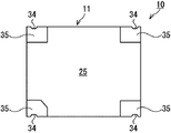
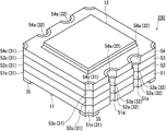
図1ないし図5は、本発明の制御端子付き電子部品(以下、「電子部品」という)の第1の実施の形態を示しており、図1はその概略斜視図、図2はその概略平面図、図3はその概略側面図、図4はその概略底面図、図5は図2のA−A線概略断面図である。
これらの図において、電子部品10は、パッケージ11と、このパッケージの内部空間S1に収容された複数の内蔵部品を備えており、内蔵部品は、この実施形態の場合には、圧電振動片15と、集積回路16である。つまり、電子部品10は、この実施形態では、圧電振動片15と、この圧電振動片15と接続された集積回路16を備える圧電発振器を構成した例が示されている。
【0043】
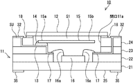
電子部品10のパッケージ11は、例えば、セラミックグリーンシートを成形して焼結した酸化アルミニウム質焼結体等を利用した複数の基板を積層して形成されている。複数の各基板は、その内側に所定の孔を形成することで、積層した場合に内側に所定の内部空間S1を形成するようにされている。
すなわち、パッケージ11は、全体として、図1に示されているように幾何学形状、例えば矩形状に形成されている。このパッケージ11は、図5に示されているように、下から順に、圧電材料の第1の基板21、第2の基板22、第3の基板23、第4の基板24を積層して形成されており、各基板の内側の材料を除くことで形成した空間を上下に連通するように、図5において階段状となるように一体化して、ひとつの内部空間S1を形成している。
【0044】
パッケージ11の上端は、第4の基板24の内側が大きく除かれることで、開放されており、開口11aとなっている。この開口11aは、蓋体12を固定するように塞がれている。尚、図1及び図2では、理解の便宜のため、この蓋体12の一部が透明であるように示して、パッケージ11内の構造が見えるようにされているが、蓋体12は完全な板状であり、開口等を形成しているものではない。
【0045】
図5に示されているように、パッケージ11の内部空間S1の底面を形成する第1の基板21の上面に設けた実装箇所には、集積回路16が固定されており、第2の基板22の上面に例えば、金または金合金で形成した電極部17,17に対して金線16a,16a等を用いてワイヤボンディングされている。
そして、この電極部17,17は、第3の基板23の上面に形成した電極部13,13と一体化されており、この電極部13,13の上には、圧電振動片15がマウントされている。
【0046】
圧電振動片15は、例えば水晶で形成されており、水晶以外にもタンタル酸リチウム,ニオブ酸リチウム等の圧電材料を利用することができる。本実施形態の場合、圧電振動片15は、水晶の薄い矩形状の板体で形成された、所謂ATカット振動片であり、その表面には、図示しない励振電極が形成されている。圧電振動片15は、このような形態以外にも、マウント部である基部と、この基部から一方向に向けて、二股に別れて平行に延びる一対の振動腕を備える、全体が音叉のような形状とされた、所謂、音叉型圧電振動片等が利用されてもよい。
【0047】
圧電振動片15は、基端部15aが、導電性接着剤14を介して、電極部13に接合されており、電極部13と電気的に接続されている。導電性接着剤14は、例えば、接合力を発揮する接着剤成分としての合成樹脂剤に、銀製の細粒等の導電性の粒子を含有させたものである。
【0048】
この圧電振動片15がマウントされた電極部13は、図5に示すように、最上段の積層基板である第4の基板24の上面まで引き回されて外部に露出され、図1及び図2に表れているように、制御端子32が設けられている。この制御端子は、この実施形態では、パッケージ11の上端の蓋体12を挟んで、両側の周縁部に2つずつ、全部で4つの制御端子32,32,32,32とされている。これら4つの制御端子32,32,32,32は、図1に示されているように、パッケージ11のひとつの面SUである上面に向いて、形成されている。
【0049】
パッケージ11の底面25には、図4に示されているように、各角部に実装端子35,35,35,35が形成されている。この実装端子35,35,35,35は、図示しない経路により、パッケージ11内の電極部17に接続されている。
【0050】
さらに、図5に示す実装端子35,35,35,35は、それぞれ、パッケージ11の外壁面をパッケージ11の厚み方向に延びる溝または凹部に形成した、導体部34,34,34,34により、パッケージ11の上端面まで引き回されている。
そして、パッケージ11の上端面の各角部には、図1及び図2に示されているように、上記導体部34,34,34,34により、図5の各実装端子35,35,35,35に接続された検査用端子31,31,31,31が設けられている。
したがって、これら検査用端子31,31,31,31も、実装端子35,35,35,35が形成された底面25と反対面であるパッケージ11のひとつの面SUとしての上面に向いて、形成されている。
【0051】
パッケージ11の開放された上端には、上述したように、ロウ材18を介して、蓋体12が接合されることにより、封止されている。蓋体12は、例えば、コバール等のパッケージ11と熱膨張係数の近似した材料で形成することができる。
【0052】
本実施形態は以上のように構成されており、パッケージ11の実装面である底面25実装端子35,35,35,35と接続された検査用端子31,31,31,31と制御端子32,32,32,32が、ともにパッケージ11の上面SUに形成されている。このため、制御端子32,32,32,32も、検査用端子31,31,31,31も実装端子35,35,35,35と異なる面に設けられているから、電子部品11が小型化されても、実装用の半田(図示せず)により実装基板(図示せず)と検査用端子31,31,31,31も、あるいは制御端子32,32,32,32も、実装端子と短絡されることがない。したがって、検査用の端子を設けても、製品の品質に悪影響を受けることがない。
【0053】
また、制御端子32,32,32,32と検査用端子31,31,31,31が、ともに、パッケージ11の上面SUに向かって露出されているので、向きを揃えた検査用のピンを備える検査治具により、容易に検査することができる。したがって、検査治具の構成が単純ですみ治具に要する費用を安価にできると共に、検査が迅速かつ確実に行える。
【0054】
特に、この実施形態では、パッケージ11には内部空間S1と連通した開放部もしくは開口11aがあり、この部分が蓋体12で塞がれている。そして、この蓋体12が固定されるパッケージ11の上面SUに、制御端子32,32,32,32と検査用端子31,31,31,31が、その向きをそろえられて露出されている。このため、パッケージ11の実装面である底面25を下とした場合に、制御端子32,32,32,32と検査用端子31,31,31,31に対しては、図1に示すように、パッケージ11の上方から検査用のピン39,39,39,39,39,39,39,39を容易に当てることができる。
【0055】
また、パッケージ11の内部空間S1内に、縦方向に沿って、圧電振動片15と集積回路16とが配置されているから、複数の内蔵部品を収容していても、電子部品10全体として、実装基板の実装面積を大きくとることがない。
【0056】
また、図1及び図2に示されているように、この実施形態では、パッケージ11の上端,すなわち、第4の基板24の上面の蓋体12周囲のスペースを有効に利用して、制御端子32,32,32,32と検査用端子31,31,31,31とを形成できると共に、これらの端子がパッケージ端面に高さをそろえて露出することになるので、検査用ピンの構成が一層簡単になり、検査もしやすくなる。
さらに、この実施形態では、パッケージ11のひとつの内部空間S1内に、縦方向に沿って、圧電振動片15と集積回路16とが配置されているから、内蔵部品の収容スペースを共通化する構成とすることができ、パッケージ11の構成を単純化できる。
【0057】
図6ないし図9は、第1の実施形態の変形例1を示しており、図6はその概略斜視図、図7はその概略平面図、図8はその概略側面図、図9はその概略底面図である。
これらの図において、図1ないし図8の電子部品10と同一の符号を付した箇所は共通の構成であるから、重複する説明は省略し、以下、相違点を中心に説明する。
【0058】
図6ないし図9において、変形例1に係る電子部品20は、電子部品10と比較すると、導体部36の構成のみが異なっている。
すなわち、電子部品20においては、検査用端子31,31,31,31と、実装端子35,35,35,35とを電気的に接続する導体部36,36,36,36は、パッケージ11の四隅に縦方向に沿って形成されたキャスタレーションの表面に形成されている。
このキャスタレーションは、各基板21,22,23,24を焼結後、パッケージに形成された高融点のタングステン等からなるパターンに、NiあるいはAu等をメッキ形成する際に、対応したメッキ液に、パッケージをつける場合、メッキすべき箇所の表裏にメッキ液がまわりやすくするためのものである。また、この電子部品20を実装基板に実装した際に、実装基板のランド(図示しない)と実装端子35の半田による接合強度を得るために、このキャスタレーションに導体をメッキし、この部分にも半田接合させることで、上記接合強度を向上させることができる。
【0059】
そして、図示するように、基板の四隅の箇所に、1/4円の形状のキャスタレーションが形成されるので、パッケージ11をつくる際に、第1ないし第4の基板21,22,23,24を図示するように重ねると、各基板21,22,23,24の四隅の1/4円の形状のキャスタレーションが、パッケージ11の厚み方向に連続する。この連続するキャスタレーションを利用してその表面に導体金属による導体部36,36,36,36を形成すれば、検査用端子31,31,31,31と、実装端子35,35,35,35との接続構造を容易に形成することができる。
また、パッケージ31の四隅の角に導体部36を形成することにより、側面のパッケージ壁厚が十分確保されるため、電子部品20の小型化が進んだ場合にも、パッケージ側面の強度を保つことができる。
変形例1のその他の作用効果は、第1の実施形態と同様である。
【0060】
図10は、第1の実施形態の変形例2を示しており、図10において、図1ないし図8の電子部品10と同一の符号を付した箇所は共通の構成であるから、重複する説明は省略し、以下、相違点を中心に説明する。
図10において、電子部品30は、図1ないし図8の電子部品10と比べると、パッケージ11を構成する積層基板の構造が異なっている。
【0061】
すなわち、電子部品30のパッケージ11を構成する第1の基板311と、第2の基板312には異なる大きさに、内側の材料が除かれている。第3の基板313は内側の材料を除かないで、孔のない基板とされており、第4の基板314は内側の材料が除かれている。
これにより、第1の基板311と、第2の基板312の内側には、第1の内部空間S2が形成され、第4の基板314の内側には、第2の内部空間S3が形成されている。第3の基板313は、これら第1の内部空間S2と第2の内部空間S3を上下に区分する境界を形成している。
【0062】
第1の内部空間S2には、集積回路16が第3の基板313の図において下面に対して固定されており、金線16a,16aを用いて、電極部17,17に対してワイヤボンディングされている。電極部17は、電子部品10の場合と同様に制御端子32に接続されている。
さらに、内部空間S2には、合成樹脂33を充填することにより、樹脂モールドされている。
第2の内部空間S3には、圧電振動片15が電極部13上に導電性接着剤13を介してマウントされている。電極部13は、電子部品10の場合と同様に制御端子32に接続されている。
【0063】
このように、変形例2によれば、内部空間が、基板を挟んで上下に分割された2つの空間S2,S3とされている。そして、第3の基板313の両面側に電極13と電極17をそれぞれを形成することで、圧電振動片15と集積回路16を、第1の内部空間S2と第2の内部空間S3の2つの各空間に収容する構造を実現でき、これらの内蔵部品を縦方向に収容することで、実装スペースの有効な利用ができる。また、圧電振動片15と集積回路16を実装する空間S2とS3が第3の基板313によって分離されるので、ノイズを遮蔽しやすい利点がある。その他の作用効果は、電子部品10と同じである。
【0064】
図11は、第1の実施形態の変形例3を示しており、図11において、図1ないし図8の電子部品10と同一の符号を付した箇所は共通の構成であるから、重複する説明は省略し、以下、相違点を中心に説明する。
図11において、電子部品200は、図1ないし図8の電子部品10と比べると、パッケージ11を第1のパッケージとして、さらに、第2のパッケージ201備える点が異なっている。
【0065】
下側のパッケージである第1のパッケージ11は、電子部品10のパッケージ11と同じ構造であり、その内部空間である第1の内部空間S4には、電子部品10の場合と同様に、集積回路16が収容されている。
第1のパッケージ11の第4の基板24の開口11aには、第2のパッケージ201がはめ込まれて、固定されている。
上側のパッケージである第2のパッケージ201は、図示されているように第1のパッケージ11よりも小さく形成されている。この第2のパッケージ201は、例えば、2枚の積層基板を利用して形成されており、第1の基板37の上に、内側の材料を除いた第2の基板38が重ねられている。第2の基板38の内側に形成されている第2の内部空間S5には、圧電振動片15が収容されており、この第2の基板38には、ロウ材18を介して蓋体12が固定されている。
【0066】
第1のパッケージ11の開口11aには、第2のパッケージ201がはめ込まれて固定され、第1のパッケージ11と第2のパッケージ201は一体化されている。そして、大きなサイズの第1のパッケージ11に、これよりも小さな第2のパッケージ201を重ねたことにより、固定箇所の第2のパッケージ201の周縁より外側に、段部が形成され、この上向きの段部であるひとつの面SUには、電子部品10と同様に、検査用端子31と制御端子32が設けられている。したがって、この変形例3においても、検査用端子31と制御端子32は、第1のパッケージ11の実装端子35,35が形成された実装面と反対の面SUに向くように露出されている。
【0067】
第1の実施形態の変形例3は、以上のように構成されており、変形例2と同様に、内蔵部品を縦方向に収容することで、実装スペースの有効な利用ができる。また、圧電振動片15と集積回路16とが、異なるパッケージに収容されてひとつの電子部品200を構成することで、より一層ノイズの遮蔽効果がある。
【0068】
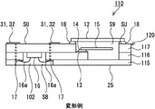
図12ないし図15は、第1の実施形態の変形例4を示しており、図12はその概略平面図、図13はその概略側面図、図14はその概略底面図、図15は図12のB−B線概略断面図である。
これらの図において、図1ないし図8の電子部品10と同一の符号を付した箇所は共通の構成であるから、重複する説明は省略し、以下、相違点を中心に説明する。
図12ないし図15において、変形例4に係る電子部品210は、電子部品10と比較すると、主に、蓋体12を実装面側に配置し、内蔵部品である集積回路16をパッケージ218の上面に配置した構成が異なっている。
【0069】
すなわち、電子部品210においては、図15に示されるように、パッケージ218は、下から第1の基板218a、第2の基板218b、第3の基板218cを積層して形成されており、第2の基板218bに所定の孔211を設けることで、内部空間S1が形成されている。この内部空間S1内の最上段の基板である第3の基板218cには、電極部13が下向きに設けられており、この電極部13に導電性接着剤14を用いて、下向きに圧電振動片15が接続されている。
【0070】
パッケージ218の最下段の基板である第1の基板218aには、第2の基板218bに設けた孔211よりも大きな孔212を設けることにより、段部213が形成されている。そして、この段部213,213にロウ材18を適用して、第2の基板218bの開口端面213,213が蓋体12により封止されるようになっている。また、パッケージ218の第1の基板218aは、孔212を設けることにより下向きの開口端面215が形成され、この開口端面215は蓋体12と同一あるいは下方に位置するように形成されている。そして、図14および図15に示されるように、この開口端面215の4隅に実装端子35,35,35,35が設けられている。
この実装端子35,35,35,35は、図13に示されるように、導体部34,34により、パッケージ218の上面SUまで引き回されて、図12に示されるパッケージ218の上面SUに設けられた検査用端子31,31,31,31と電気的に接続されている。
【0071】
また、パッケージ218の上面SUには、図15に示されるように、集積回路16が配置されている。この集積回路16は、導電性接着剤214,214を用いて圧電振動片15と電気的に接続されている。すなわち、第3の基板218cにはスルーホール217が形成されており、このスルーホール217内には導通体219が充填されており、この導通体219が圧電振動片15と接続された電極部13と電気的に接続されている。ここで、導電性接着剤214をボンディングワイヤ等に置き換えてもよい。なお、集積回路16は、非導電性の接着剤216により、パッケージ218の上面SUに固着するようになっており、またコーティング(図示せず)等をすることにより絶縁されるようになっている。
そして、パッケージ218の上面SUには、図12に示されるように、制御端子32,32,32,32が配置されており、これらの制御端子32,32,32,32は、上面SUを引き回されて、同一面SUに配設された集積回路16と電気的に接続されている。なお、非導電性の接着剤216にて検査用端子31および制御端子32を覆ってしまい、検査及び調整ができない恐れがあるため、図12のように接着剤216からある程度離れた部分に検査端子31および制御端子32が配置されることになる。しかし、集積回路16に対して電子部品210が小さい場合には、検査用端子31及び制御端子32が小さくなってしまい、検査用のピンとの接触が十分に取れない場合がある。この場合には、検査等を行なった後に接着剤216を塗布するようにすれば、検査用端子31及び制御端子32を接着剤216より離す必要がないため、検査用端子31及び制御端子32の端子面積を大きくすることができる。また、接着剤216によって、検査及び調整後に検査用端子31及び制御端子32を覆うことができる。
【0072】
第1の実施形態の変形例4は以上のように構成されており、蓋体12を実装面側に配置するようにして、集積回路16をパッケージ218の上面SUに設けることにより、同一面SUに設けられた制御端子32,32,32,32と集積回路16とを容易に電気的に接続することができる。
【0073】
図16ないし図20は、本発明の制御端子付き電子部品の第2の実施の形態を示しており、図16はその概略斜視図、図17は図16のC−C線概略断面図、図18はその概略平面図、図19はその概略側面図、図20はその概略底面図である。尚、図17では、理解の便宜のため、第1のパッケージ41の一部が透明であるように示して、第1のパッケージ41内の構造が見えるようにされているが、第1のパッケージ41は透明体ではない。
【0074】
これらの図において、図1ないし図8の電子部品10及び第1の実施形態の変形例の説明と同一の符号を付した箇所は共通の構成であるから、重複する説明は省略し、以下、相違点を中心に説明する。
第2の実施形態に係る電子部品40は、例えば、全体として、直方体形状,すなわち平面視で、図18に示されているように、4角形状もしくは長方形状に形成されている。この電子部品40は、上側となる第1のパッケージ41と、下側となる第2のパッケージ42を備えている。すなわち、第1のパッケージ41と、第2のパッケージ42は、図16に示すように縦方向に重ねて固定されるようになっている。
【0075】
具体的には、図16及び図17に示すように、第1のパッケージ41は、集積回路16を、例えばモールド樹脂などの絶縁部材により覆うようにしている。集積回路16は、図17に示されているように、第1のパッケージ41の上面側を下にして固定されている。一方、第1のパッケージ41の各角部には、導電性を備えて、かつバネ弾性を発揮する金属により、検査端子31,31,31,31が形成されている。各検査端子31,31,31,31は、パッケージ41の上面SUに露出する部分が端子として機能するとともに、第1のパッケージ41の外側側面に沿って、それぞれ下方へ板バネ状に延長されて、係止手段31a,31a,31a,31aを形成している。各係止手段31a,31a,31a,31aは、先端側が内方に向くように付勢されている。また、各検査端子31,31,31,31は、係止手段31a,31a,31a,31aと反対側の先端部31bが絶縁部材により覆われており、第1のパッケージ41から抜けてしまわないようになっている。
そして、第1のパッケージ41内の集積回路16は、金線16a,16aによって、パッケージ内部で、これら各検査用端子31,31,31,31と接続されている。
【0076】
また、第1のパッケージ41の上面SUの中央よりには、制御端子32,32,32,32,432,432が露出されている。これら制御端子32,32,32,32,432,432についても、金線16b,16bによって、集積回路16と接続されている。なお、制御端子32,32,32,32,432,432の内、制御端子432,432については、検査用端子31と略同様の形状から構成された係止手段432aを形成している。
【0077】
第2のパッケージ42の上には、蓋体12が固定されている。尚、図16では、理解の便宜のため、蓋体12を通して、内部の構成を示している。そして、第2の内部空間S7には、圧電振動片15が収容されており、第1の実施形態と同じようにマウントされている。また、第2のパッケージ42の角部には、キャスタレーションが形成され、その上に底面25の各実装端子35,35,35,35と接続された導体部36が設けられている。なお、第2のパッケージ42の側面にもキャスタレーションが形成され、その上に、第2のパッケージ42の内部配線により、電極部13と電気的に接続された導体部436が設けられている。このようにして、集積回路16と圧電振動片15とは、第1のパッケージ41の制御端子432,432及び第2のパッケージ42の導体部436を介して電気的に接続されている。
【0078】
以上の構成において、図16に示されているように、第2のパッケージ42の上から第1のパッケージ41を被せるように、矢印方向に移動させると、第2のパッケージ42の上に第1のパッケージ41が重なり、各係止手段31a,31a,31a,31aは、第2のパッケージ42の各導体部36に重なって内方に付勢する。
これにより、第1のパッケージ41が第2のパッケージ42に重ねた状態で固定されると共に、各係止手段31a,31a,31a,31aは、第2のパッケージ42の導体部36と電気的に接続される。
【0079】
本実施形態は以上のように構成されており、第1の実施形態と同様の作用効果を発揮するとともに、第1のパッケージ41に集積回路16を収容することで、第1のパッケージ41には、蓋体を設ける必要がなく、その分スペースを有効利用して、上面SUに制御端子を設けることができる。また、この第1のパッケージ41は、簡単な作業により係止手段31a,31a,31a,31aを用いて、簡単な作業で、第2のパッケージ42に係止できる。この係止手段31a,31a,31a,31aは導電性であり、一部が第1のパッケージ41上面SUに露出され、しかも第2のパッケージ42の導体部36と接触されることで、第1のパッケージ41の上面SUに検査用端子31,31,31,31を簡単に形成することができるという巧みな構造とすることができる。
【0080】
図21および図22は、第2の実施の形態に係る変形例を示しており、図21はその概略斜視図、図22は図21のD−D線概略断面図である。尚、図22では、理解の便宜のため、第1のパッケージ41の一部が透明であるように示して、第1のパッケージ41内の構造が見えるようにされているが、第1のパッケージ41は透明体ではない。
これらの図において、図16ないし図20の電子部品40の説明と同一の符号を付した箇所は共通の構成であるから、重複する説明は省略し、以下、相違点を中心に説明する。
図21および図22において、変形例に係る電子部品220は、電子部品40と比較すると、主に検査用端子31周辺の形状が異なっている。
【0081】
すなわち、電子部品220においては、第1のパッケージ41は、係止手段31a,31a,31a,31aが第1のパッケージ41から外れてしまわないように、係止手段31a,31a,31a,31aの一部(図22においては係止手段の第1のパッケージ41側の先端部)を絶縁部材により覆うようにしている。また、これらの図では、制御端子432に接続されている係止手段432aについても、絶縁部材により覆われている。
そして、この第1のパッケージ41を形成する絶縁部材は、図22に示されるように、上面に凹部222,222,222,222を形成して、絶縁部材により覆われた係止手段31a,31a,31a,31aの一部を、第1のパッケージ41の上面SUに露出させている。このようにして、第1のパッケージ41の上面SUに露出させた係止手段31a,31a,31a,31aを、検査用端子31,31,31,31としている。
【0082】
本第2の実施形態の変形例は、以上のように構成されており、このため、検査用ピンを検査用端子31,31,31,31に当てる際、凹部222,222,222,222が検査用ピンを検査用端子31,31,31,31まで案内するガイドとなり、確実に検査を行うことができる。
【0083】
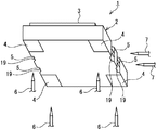
図23ないし図25は、本発明の制御端子付き電子部品の第3の実施の形態を示しており、図23はその概略斜視図、図24はその概略分解斜視図、図25はその検査方法を説明する概略斜視図である。
これらの図において、図1ないし図8の電子部品10及び第1の実施形態の説明と同一の符号を付した箇所は共通の構成であるから、重複する説明は省略し、以下、相違点を中心に説明する。
【0084】
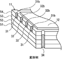
第3の実施形態に係る電子部品50は、図23及び図24に示されているように、複数の基板を積層してパッケージ11を形成している。このパッケージ11を形成するための基板は、下から第1の基板51,第2の基板52,第3の基板53,第4の基板54であり、これらの基板の材料や構造は、第1の実施形態の積層基板と同じである。
【0085】
この電子部品50では、第1の実施形態と比較すると、検査用端子31,31,31,31及び制御端子32,32,32,32が形成される箇所が異なっている。
図24に示されているように、第3の基板53において、その表面の左右端部に、これら検査用端子31,31,31,31及び制御端子32,32,32,32が形成されている。
すなわち、検査用端子と制御端子は、第3の基板53の上面の左右端部にそれぞれ同じ形態で同じ数だけ設けられており、その片方、例えば左端側について説明すると、圧電振動片15の接続されている電極部13,13は、そのまま内部空間S1から外側に延長されて、延長端が並列的に並んだ制御端子32,32とされている。
【0086】
また、図示されているように検査用端子31,31は、第3の基板53の上面で、制御端子32,32の外側にひとつずつ並んで設けられている。
この制御端子32,32は、パッケージ11の内方へ向かって第3の基板53の上面を延長されており、一体に形成した電極部13,13とされている。この電極部13,13には、導電性接着剤14,14を介して、圧電振動片15が接続されている。
検査用端子31,31は、第3の基板53の上面で、制御端子32,32の外側に配置されており、内側がパッケージ11の内方へ延長され、途中で外側に90度向きを変えて、外方へ向かって延びている。そして、検査用端子31,31の延長端は、パッケージ11の厚み方向に沿って、下から第1の基板51,第2の基板52,第3の基板53にわたって形成された溝または凹部に設けた導体部34と接続されている。この導体部34は、パッケージ11の底面に設けた図示しない実装端子(図4と同じ構造)と接続されている。
【0087】
そして、パッケージ11の最上段の第4の基板54の周縁には、切り欠き部55,55,55,55が形成されている。この切り欠き部55,55,55,55は下段の基板である第3の基板53に形成された各端子部の位置に対応して設けられている。
【0088】
本実施形態は以上のように構成されており、第1の実施形態と同様の作用効果を発揮する。
図25に示すように、電子部品50に使用される検査用ピン59,59,59,59,59,59,59,59は、全て同じ形状であり、第1の実施形態における検査用ピン39(図1参照)と比べると、端子にコンタクトされる先端が、フック状とされており、このフック状の先端が、電子部品50の各切り欠き部55に入り込んで、位置決めされつつ、対応する端子部に当接するようになっている。そして、各検査用ピン59は、ひとつの面SUに対して、対向するように、全て一方向に揃えて検査することができる。
【0089】
このように、電子部品50は、第1の実施形態と共通する作用効果を発揮する他、以下のような独自の作用を発揮する。
すなわち、電子部品50においては、最上段の基板54には、蓋体12が固定されている。そして、下段の基板である第3の基板53が形成する内部空間S1に圧電振動片15が収容されることになるので、この下段の基板53上で図示されているように、電極部13を外側に延長するだけで、制御端子32がを容易に設けられる。しかも、最上段の基板である第4の基板54の周縁部に切り欠き部55を形成することで、制御端子32がひとつの面SUの方向へ上方を向いて露出される。したがって、下段の基板である第3の基板53に制御端子32に並べて検査用端子31を配置すれば、制御端子32と検査用端子31が同じ高さに揃えられて、形成されることになる。
これにより、パッケージ11上端,すなわち、第4の基板54の上面に制御端子32と検査用端子31を形成する必要がなく、蓋体12の周囲の面積は小さくてよいので、その分パッケージを小型化できる。
【0090】
図26は、第3の実施形態の第1の変形例を示しており、次の点以外は上述の説明による構成と同じである。
この場合、第4の基板54に設けた切り欠き部55の内面に、対応する端子部と一体とされた導体部31b,31b,32b,32bを備えている。これにより、図25のようにして検査を行う場合、検査用ピン59が、導体部31b,31b,32b,32bに接触することでも検査が可能であるから、検査がその分容易で、確実になる。
【0091】
図27は、第3の実施形態の第2の変形例に係る電子部品230である。
この図において、図23ないし図26に係る第3の実施形態およびその変形例と同一の符号を付した箇所は共通の構成であるから、重複する説明は省略し、以下、相違点を中心に説明する。
本第3の変形例に係る電子部品230は、そのパッケージ11を構成する第1ないし第4の基板51,52,53,54の側面に、キャスタレーション51a,52a,53a,54aが設けられている。このキャスタレーション51a,52a,53a,54aのうち、少なくとも第1の基板(実装端子側である最下段の基板)に設けられたキャスタレーション51aを除いたキャスタレーション52a,53a,54aに制御端子32が設けられている。また、本第3の変形例では、第4の基板54に設けられたキャスタレーション54aが最も大きく形成されている。
また、第1ないし第4の基板51,52,53,54の角部にも、キャスタレーション51c,52c,53c,54cが設けられており、このキャスタレーション51c,52c,53c,54cには、実装端子35と電気的に接続される検査用端子31が設けられている。
【0092】
このような電子部品230は、次のように製造されて調整検査等されている。図28は、電子部品230に係る製造方法の特徴的な部分を示す概略斜視図であり、電子部品230,230に対応するパッケージ11,11が一体となっている図である。すなわち、パッケージ11,11は、複数のシート状の絶縁材料236,237,238,239を厚み方向に積層し、これを切断して形成するようになっている。
【0093】
具体的には、例えば所謂セラミックグリーンシートを、一方向に長いテープ状に形成し、これを製造しようとするパッケージ11の数に対応してカットしてシート状の絶縁材料236,237,238,239を形成する。なお、絶縁材料236は複数の第1の基板51を、絶縁材料237は複数の第2の基板52を、絶縁材料238は複数の第3の基板53を、絶縁材料239は複数の第4の基板54を形成するベースとなる。
【0094】
次いで、シート状の絶縁材料236,237,238,239に、第1ないし第4の基板に必要な構成(図24に示す内部空間S1を形成するための孔や電極部13,13等)を、製造しようとする電子部品の数だけ形成する。
この際、シート状の絶縁材料236,237,238,239のそれぞれに、図28のE−E線概略断面図である図29に示す貫通孔236a,237a,238a,239aを、完成後の複数個の電子部品230,230どうしの境界となる位置(図28の切断線CL)に、各パッケージ11,11に跨るようにして形成する。また、本第3の変形例では、絶縁材料239に形成した貫通孔239aを最も大きく形成している。これらの貫通孔236a,237a,238a,239aは、各電子部品230,230を完成させた場合に、図27に示す側面のキャスタレーション51a,52a,53a,54aとなる。そして、これらの貫通孔のうち、複数の第1の基板51(実装端子側である最下段の基板)を形成するための絶縁材料236に形成した貫通孔236aを除いた貫通孔237a,238a,239aの内面に、導通可能な金属をメタライズなどして図29に示すように制御端子32を設ける。
また、シート状の絶縁材料236,237,238,239のそれぞれに、図28に示す切り欠き部234,234を、完成後の複数個の電子部品230,230どうしの境界となる位置(図28の切断線CL)であって、各パッケージ11,11の角部となる位置に、各パッケージ11,11を跨るようにして形成する。この切り欠き部234,234は、各電子部品230,230を完成させた場合に、図27に示すキャスタレーション51c,52c,53c,54cとなる。そして、この切り欠き部234,234には、全面に検査用端子31,31を設ける。
【0095】
次いで、絶縁材料236,237,238,239を積層した後、既に形成した複数の内部空間S1内のそれぞれに内蔵部品15,16を収容固定して、蓋体12により封止する(図24参照)。その後、図28に示すように、検査用ピン39,39,39,39を複数個の電子部品230,230どうしの境界(切断線CL)に沿うようにして降下させ、制御端子32,32および検査用端子31,31に接触させる。そして、図28に示す切断線CLに沿って切断分離し、パッケージ11,11を完成すると共に電子部品230,230を完成する。
【0096】
本第3の実施形態の第2の変形例は以上のように構成されている。これにより対応する複数個の電子部品が連続するようにされたシート状の絶縁材料を複数層積層した状態において、制御端子32,32および検査用端子31,31は、各電子部品230,230に共通する端子となっているため、複数の電子部品230,230を同時に調整検査等することができ、内蔵部品の調整検査等を迅速に行える。
また、絶縁材料239に形成した貫通孔239aは他の貫通孔236a,237a,238aよりも大きく形成されているため、絶縁材料236,237,238,239を積層した状態において、図28に示すように、凹状となっている。したがって、この凹状が検査用ピン39,39を制御端子32,32に案内して、確実に検査用ピン39,39を制御端子32,32に接触させることができる。また、確実に検査用ピン39,39を制御端子32,32に接触させることができれば、検査用端子31,31と制御端子32,32の距離は決まっているので、検査用ピン39,39を検査用端子31,31に確実に導くことができる。
【0097】
尚、図30(a)(b)(c)は、上述した貫通孔に設けた検査用端子31の配設パターンの変形例であり、これらの図に示されるように、隣接する完成前の各電子部品230,230に共通する検査用端子31を形成することができれば、検査用端子31の配設パターンは上述した配設パターンに限られない。
また、図28および図29は、作図の便宜上、2つの完成前の電子部品230,230どうしの境界となる部分を拡大した図であるが、他にも複数の電子部品230,230・・・が連続しており、制御端子32,32および検査用端子31,31は、隣接する各電子部品230,230・・・に共通する端子となるように設けられている。
【0098】
図31及び図32は、本発明の制御端子付き電子部品の第4の実施の形態を示しており、図31はその概略斜視図、図32はその検査方法を説明する概略側面図である。
これらの図において、図1ないし図8の電子部品10及び第1の実施形態の説明と同一の符号を付した箇所は共通の構成であるから、重複する説明は省略し、以下、相違点を中心に説明する。
【0099】
本実施形態の電子部品60は、パッケージの形態が異なる他、第3の実施形態と共通の構造である。パッケージ61を構成する第1ないし第3の基板51,52,53の構造は、第3の実施形態と同じであり、圧電振動片及び集積回路の収容構造や電極の設け方も同じである。
電子部品60のパッケージ61では、第3の基板53の上に重ねられる基板が、第3の実施形態よりも一枚多く、第4の基板64と第5の基板65を有している。少なくとも第4の基板64は、内部空間を形成するように、内側の材料が除去されており、最上段の基板である第5の基板65は、上記内部空間と連通する空間を有していてもよいし、内部空間を形成しなくてもよい。
【0100】
この実施形態で特徴的なのは、蓋体12が固定されている最上段の基板である第5の基板65の下段の基板である第4の基板64の外形が他の基板よりも小さくされることで、凹部形成基板とされている点である。すなわち、第4の基板64の箇所には、外周が内側に凹状となった凹部68が形成されている。
このため、この凹部68には、検査用端子31,31と制御端子32,32が、パッケージ61上面SUに向かって露出されている。
【0101】
本実施形態は以上のように構成されており、検査の際には、図32に示されているように、電子部品60の両側に配置された検査装置の検査用ピンの移動手段66,66が、電子部品60に接近される。そして、矢印で示すように縦方向に回動される検査用ピン67,67が電子部品60の両側に形成された凹部68,68内に入り込んで、各先端が、検査用端子31及び制御端子32と接触される。
したがって、この実施形態の場合も、第1の実施形態と同様に、一方向に向いた検査用ピン67,67により、容易に検査を行うことができるので、第1の実施形態と同様な作用効果を発揮することができる。
【0102】
しかも、最上段の基板65は、図示されているように、蓋体12が固定され、それより下段の基板が形成する内部空間に圧電振動片が収容されることになるので、この下段の基板上で水平に電極部を外側に引き回せば、第3の実施形態と同様に、制御端子32を容易に設けられる。この場合、最上段以外の基板64の外縁部が他の基板よりも内側に位置する形状とされることで、パッケージ65側面に凹部68を形成する凹部形成基板とされることで、この凹部68において、制御端子32が上方を向いて露出される。したがって、下段の基板53の上面に検査用端子31を配置すれば、制御端子32と検査用端子31が同じ高さに揃えられて、形成されることになる。これにより、パッケージ65上端に制御端子32と検査用端子31を形成する必要がなく、その分パッケージ65を小型化できる。そして、例えば、前記凹部68内で、縦方向に旋回する検査用ピン67を利用することにより、容易に検査を行うことができる。
この実施形態の場合、特に最上段の基板65には、第3の実施形態のように切り欠き部さえ形成する必要がないので、蓋体12を固定できる最低の大きさがあれば済むことから、電子部品60の平面的大きさをさらに小さくすることができる。
【0103】
図33ないし図34は、本発明の制御端子付き電子部品の第5の実施の形態を示しており、図33はその蓋体をはずした状態の概略斜視図、図34はその全体を示す概略斜視図、図35は、その蓋体の概略平面図、図36はその蓋体の概略側面図、図37は、その蓋体の概略底面図である。
これらの図において、図1ないし図8の電子部品10その他の実施形態の説明と同一の符号を付した箇所は共通の構成であるから、重複する説明は省略し、以下、相違点を中心に説明する。
【0104】
図33において、本実施形態のパッケージ71の構造は、図24で説明したパッケージ11の構造とほぼ同じであり、積層基板や内蔵部品についての説明は省略する。
第5の実施形態にかかる電子部品70において特徴的な点は、制御端子と検査用端子を蓋体に形成したために、パッケージの大きさを最も小さく形成できる点である。
【0105】
図33に示されているように、パッケージ71は、平面視において、例えば、ほぼ長方形状に形成されている。このパッケージ71の上端面75には、その外縁部に近い位置に、パッケージ側導体部として、複数の電極部73が形成されている。そして、各電極部の周囲を囲むように、導体を形成しない領域として絶縁部74が形成されている。
具体的には、パッケージ71側の導体面である電極部73は、長方形の各隅部と、各隅部の中間位置で、長方形の各辺の中央近傍にそれぞれ図示のように形成されている。各隅部に設けた電極部73は、図24の構造と同様にして、パッケージ内部を経由して、パッケージ71側面にて縦方向に延びる各導体部34と接続されており、後述する蓋体76の検査用端子と接続される。各隅部の中間、すなわち、長方形の各辺の中央付近に形成されている電極部73は、図24の第3の基板53の構成として説明したように、内蔵部品と接続されて、引き回され、図24の場合とは異なり、最上段の基板72の上端面75に延長して、図23のように形成されている。
【0106】
蓋体76は、ガラスのような非導電性の材料、もしくは圧電材料等により形成されている。図33と図35に示すように、蓋体76の表面(上面)には、制御端子と、検査用端子が複数形成されている。
具体的には、ほぼ長方形でなる蓋体76の各角部もしくは隅部には、それぞれ検査用端子31,31,31,31が形成されており、各検査用端子31どうしの間の位置で、蓋体76の外縁に沿って、制御端子32,32,32,32が形成されている。この各制御端子と検査用端子の位置は、図33のように、パッケージ71に対して、蓋体76を固定する位置に合わせた場合に、パッケージ71側の上述した対応する電極部73と位置合わせされるようになっている。
さらに、図33及び図35に示されているように、検査用端子31,31,31,31及び制御端子32,32,32,32のうち、いずれかの端子部に異形部を設けている。例えば、この実施形態の場合、図35の左下の検査用端子31の一部を他の端子部の形状と異なる形状とした異形部31eを設けていることで、図33のように、パッケージ71に蓋体76を固定する場合に、取付けに方向性を必要とする際、正しく位置合わせするための案内とすることができる。
また、異形部31eは、電子部品70を実装基板(図示せず)に実装する場合にも取付け方向を認識するための目印になる。
【0107】
また、蓋体76の各端子が形成された箇所の側面には切り欠き部がそれぞれ形成されている(図35及び図36参照)。すなわち、蓋体76の検査用端子31,31,31,31の外縁には、それぞれ切り欠き部31c,31c,31c,31cが、蓋体76の制御端子32,32,32,32の外縁には、それぞれ切り欠き部32c,32c,32c,32cが、それぞれ形成されており、各切り欠き部の内面には、対応する端子と一体の導電部が設けられている。
【0108】
さらに、図37に示すように、蓋体76の裏面には、斜線で示した領域77に、蓋体76のパッケージ71に対する接合に使用される導電性のロウ材が付着する封止しろが存在する。このため、この封止しろから絶縁するため、上記切り欠き部31c,31c,31c,31cの周囲に絶縁領域31d,31d,31d,31dが、上記切り欠き部32c,32c,32c,32cの周囲に絶縁領域32d,32d,32d,32dが、それぞれ設けられている。
【0109】
そして、図34に示されているように、パッケージ71に蓋体76を固定すると、蓋体76の上述した各切り欠き部31c,32cから、最上段の基板72上の各電極部73が露出する。したがって、各切り欠き部31c,32cの内側に、導通用の半田等をもることで、パッケージ71側の各電極部と、蓋体76の各検査用端子31と各制御端子32が電気的に接続され、蓋体76の上面をひとつの面SUとして、この上面SUに各検査用端子31と各制御端子32が露出する構成が得られる。
【0110】
本実施形態は以上のように構成されており、図34の状態の電子部品70に対して、図1の検査用ピン39と同様な検査手段を用いて、蓋体76上の各検査用端子31と各制御端子32に接触させることで、容易に検査を行うことができるので、本実施形態も第1の実施形態と同様の作用効果を発揮できる。
【0111】
しかも、各検査用端子31と各制御端子32は、パッケージ71ではなく、蓋体76に形成されるので、パッケージ71の上端面には、これらの端子を形成する領域を必要としない。このため、パッケージ71は、蓋体76を固定できる最低の大きさがあれば済むことから、電子部品60の平面的大きさを最も小さくすることができる。
【0112】
図38及び図39は、本発明の制御端子付き電子部品の第6の実施の形態を示しており、図38はその蓋体をはずした状態の概略斜視図、図39はその全体を示す概略斜視図である。
これらの図において、図33ないし図37で説明した電子部品70その他の実施形態の説明と同一の符号を付した箇所は共通の構成であるから、重複する説明は省略し、以下、相違点を中心に説明する。
【0113】
図38において、本実施形態のパッケージ81の構造は、上述した電子部品70の構造と同じであり、積層基板や内蔵部品についての説明は省略する。
第6の実施形態にかかる電子部品80において特徴的な点は、スルーホールを用いて、端子と電極間の接続構造を形成した点である。
【0114】
図38において、パッケージ81の上端面の導体面である各電極部73の中心付近には、パッケージの厚み方向に連続する貫通孔,すなわちスルーホール73bがそれぞれ形成されている。これらのスルーホール73bは、図の右下に拡大して示すように、メタライズ等により内面に導体を形成することによって、第3の基板53以下の電極部と、各電極部73とを電気的に接続している。
また、図38のパッケージ81の上端面75において、斜線で示す領域75aは、蓋体82を封止する際に、ロウ材が適用される領域であり、封止しろである。
【0115】
蓋体82の各検査用端子31と各制御端子32にも、同様にして、スルーホール31fと、スルーホール32fがそれぞれ形成されている。スルーホール31fと、スルーホール32fは同じ構造である。例えば、スルーホール31fは、図の右上に拡大して示すように、メタライズ等により内面に導体を形成することによって、第3の基板53以下の電極部と、各電極部73とを電気的に接続している。蓋体82の表面の端子部と、裏面の電極部(図示せず)を電気的に接続している。
すなわち、蓋体82は、第5の実施形態の蓋体76とは異なり、表面側の各検査用端子31と各制御端子32は、蓋体82の側面を介して裏側まで導体が形成されているわけではなく、切り欠き部を形成されていない。このため、各検査用端子31と各制御端子32のそれぞれ裏側には、メタライズ等による導体面として蓋体裏面電極部を設けている。
また、電極部73を導通性のロウ材にすれば、蓋体82を封止することにより、電極部73と蓋体82の各検査用端子31と各制御端子32が電気的に接続される。尚、スルーホール31内に導通性のペーストを塗布すれば、電極部73を導通性のロウ材にする必要がなく、また、蓋体裏面電極部を形成する必要もない。
【0116】
また、蓋体82の各検査用端子31と各制御端子32のうち、少なくとも、ひとつの端子である検査用端子31の外縁には、図39の右下に拡大して示すように、目印用切り欠き部31gが形成されている。この目印用切り欠き部31gは、蓋体82をパッケージ81に対して、正しく位置決めした場合に、パッケージ側導体面である電極部73が露出するようになっている。
【0117】
本実施形態は以上のように構成されており、蓋体82の検査用端子31及び制御端子32のスルーホール31f,32fと、パッケージ側スルーホール73bによって、蓋体82に設けた検査用端子31と制御端子32と、パッケージ側との電気的接続を適切に実現することができる。
これにより、本実施形態の第1の実施形態及び第5の実施形態と同様の作用効果を発揮できる。しかも、第5の実施形態と比べると、切り欠き部に半田を適用する必要がない分、電気的接続が容易となる。
【0118】
また、蓋体82に目印用切り欠き部31gを備えているので、蓋体82のパッケージ81に対する封止固定の際に、蓋体82をパッケージ81上に置いた場合に、目印用切り欠き部31gから露出するパッケージ側の導体面73が視認されることで、パッケージ81と蓋体82との精密な位置合わせを、容易に行うことができる。
【0119】
図40は、本発明の制御端子付き電子部品の第7の実施の形態の蓋体をはずした状態の概略斜視図である。
図において、図38ないし図39で説明した電子部品80その他の実施形態の説明と同一の符号を付した箇所は共通の構成であるから、重複する説明は省略し、以下、相違点を中心に説明する。
【0120】
図40において、本実施形態のパッケージ91の構造は、上述した電子部品70の構造とほぼ同じであり、積層基板や内蔵部品についての説明は省略する。
第7の実施形態にかかる電子部品90において特徴的な点は、蓋体92によるシールド構造を設けた点である。
【0121】
この電子部品90では、検査用端子31及び制御端子32を蓋体に設けることなく、パッケージ91の最上段の第4の基板72の上端面に形成した電極部73をそのまま端子として利用している。図示されているように、パッケージ91の最上段の第4の基板72の上端面に形成した電極部73は、第5及び第6の実施形態と同じであるから重複する説明は省略する。
【0122】
蓋体92は、この場合、例えばセラミックス等の圧電材料を用いて形成された板体であり、上記パッケージ91の各電極部73が露出されるように、対応する箇所に切り欠き部94をそれぞれ設けている。
さらに、この蓋体92の裏面の全面にシールド部98を形成している。シールド部98は、蓋体92の裏面に、接合のためにのAu−Snロウ材を被覆したものである。
【0123】
一方、この蓋体92と接合するために、パッケージ91の最上段の第4の基板72の上端面には、メタライズ部96が形成されている。メタライズ部96は、図40の右下に拡大して示すように、セラミックス製の第4の基板72の上端面の上に、例えば、タングステンまたはモリブデン96a、ニッケル96b、金96cを順次被覆して形成されている。
そして、メタライズ部96には、切り欠き部96dを設けて、下の電極部73を露出させている。電極部73とメタライズ部96との境界、例えば、切り欠き部96dの外縁の形状に沿った形態で、隔離部97を形成している。隔離部97は、ロウ材98及びメタライズ部96が下の電極部73に付着しないようにするためのものである。また、封止時のロウ材98よりも高い融点の材料で形成されている。例えば、ロウ材98がAu−Snの場合、隔離部97は、絶縁材料の低融点ガラス、ロウ材98がAgロウの場合には、隔離部97は、導電材料のタングステン等が用いられている。尚、隔離部97が導電材料の場合、電極部73と隔離部97の間に絶縁領域を設ける必要がある。
【0124】
さらに、好ましくは、蓋体92表面のパッケージ91と重なるいずれかの位置に、電極部を形成してグランド端子99を設ける。グランド端子99の中心付近には、スルーホール99aを形成し、蓋体92をパッケージ91に固定した場合に、スルーホール99aと重なる位置に、パッケージ側スルーホール93を形成する。このパッケージ側スルーホール93は、パッケージ91の底面のグランド電極と接続する。
【0125】
本実施形態は以上のように構成されており、蓋体92をパッケージ91に固定した状態で露出する各検査用端子31及び各制御端子32は、パッケージ91の上端面であるひとつの面SUに向いて露出されるから、第1の実施形態と同様の作用効果を発揮することができる。
しかも、蓋体92の裏面のほぼ全面に、導電性のロウ材を利用したシールド部を形成しているので、ノイズの発生を効果的に防止できる。
【0126】
図41ないし図44は、本発明の制御端子付き電子部品の第8の実施の形態を示しており、図41はその概略平面図、図42はその概略側面図、図43はその概略底面図、図44は図41のC−C線概略断面図である。
これらの図において、図1ないし図8の電子部品10と同一の符号を付した箇所は共通の構成であるから、重複する説明は省略し、以下、相違点を中心に説明する。
【0127】
第8の実施形態に係る電子部品100は、そのパッケージ101が、一方向に長い形態を示している。具体的には、パッケージ101は、図41において左右の方向に長い直方体に形成された例を示している。図44に示されているように、パッケージ101は、下から順に、第1の基板111、第2の基板112、第3の基板113を積層して形成したものである。そして、これらの積層した基板の一部について、その内側の材料を除くことにより、内部空間を形成するようにされている。
【0128】
すなわち、第1の基板111は、その材料を除くことなく使用され、その上に重ねた第2の基板112は、図44において、左右の2箇所の材料を除いた状態で積層され、その上に重ねた第3の基板113も、左右の2箇所の材料を除いた状態で積層されている。これにより、パッケージ101の内部が水平な方向に2つの空間S8,S9に分割されている。
内部空間S8と内部空間S9は、パッケージ101の底面25と反対の面であるひとつの面SU側が開放されている。内部空間S8内には集積回路16が収容されている。この内部空間S8の開口には、蓋体を固定することなく、モールド樹脂102が充填されている。内部空間S9には、圧電振動片15が収容されており、この内部空間S9の開口は、蓋体12を固定することにより封止されている。
【0129】
この実施形態では、パッケージ101が水平な方向に分割された内部空間S8,S9を備え、各分割された内部空間S8,S9に個々の内蔵部品を収容できるので、パッケージ101内に複数の内蔵部品を収容しても、パッケージ101の高さが増すことがなく、低背化を実現することができる。
【0130】
パッケージ101の内部空間S8側の領域には、図41に示すように、検査用端子31,31,31,31と制御端子32,32,32,32が集中的に配置されている。これらの端子とパッケージ側の電極との関係は、第1の実施形態と同じである。
これにより、本実施形態においても、検査用端子31,31,31,31と制御端子32,32,32,32が、パッケージ101のひとつの面SUに向いて露出されているので、第1の実施形態と同様の作用効果を発揮することができる。しかも、第1の実施形態のように、蓋体を挟んで両側に各端子を設けるのでなく、パッケージ101の片側に、蓋体12を避けて集中的に設けることができるので、その分検査用のピン(図示せず)の当接作業等がしやすい。
【0131】
図45は、第8の実施形態に係る電子部品100の変形例である電子部品110の概略断面図である。図45において、図44と同じ符号を付した箇所は同一の構成であるから、重複する説明は省略する。
この電子部品110が、電子部品100と異なっている点は、第1の基板115、第2の基板116、第3の基板117の内側の材料を除いた箇所を、電子部品100の積層基板と異ならせることで、内部空間の設け方を変更している点である。
【0132】
これにより、図示するように、電子部品110のパッケージ120では、内部空間9の開放部は、電子部品100の場合と同じひとつの面SU側であるが、内部空間S8の開放部は、電子部品100の場合と異なり、ひとつの面SU側と反対の底面側となっている。
これにより、蓋体12が固定された同ひとつの面SUで、内部空間S8に対応した領域が開放されていないので、検査用端子31,31,31,31と制御端子32,32,32,32を設けるべき領域を広くとることができる。その他の作用効果は、電子部品100の場合と同じである。
【0133】
図46は、本発明の第9の実施の形態に係る電子部品240の製造方法について、特徴的な部分を示した概略平面図である。
この図において、図1ないし図8の電子部品10と同一の符号を付した箇所は共通の構成であるから、重複する説明は省略し、以下、相違点を中心に説明する。
【0134】
図46に係る電子部品240は、電子部品240を完成する直前の構成が、実装端子35,35,35,35の大きさが異なっている点を除いては、第1の実施形態に係る電子部品10と略同様となっている。
すなわち、この電子部品240において特徴的なところは、電子部品240を製造するにあたって、実装端子35,35,35を検査用端子31,31,31,31よりも大きく形成しておく。そして、検査用端子31,31,31,31および制御端子32,32,32,32を用いて内蔵部品15,16(図5参照)を調整および検査する。その後、配設した実装端子35,35,35の一部を残すようにして、パッケージ11の検査用端子31,31,31,31および制御端子32,32,32,32が設けられた領域E,Eを、切断する。
【0135】
本第9の実施形態は以上のように構成され、このため、電子部品240を完成させた後に不要となった検査用端子31,31,31,31および制御端子32,32,32,32を取り除くことができる。そして、検査用端子31,31,31,31および制御端子32,32,32,32を取り除く際、パッケージ11の検査用端子31,31,31,31および制御端子32,32,32,32が配設された領域E,Eを切断しているため、パッケージ11を小型化できる。
【0136】
図47は、本発明の上述した各実施形態に係る電子部品としての圧電デバイス,特に圧電発振器を利用した電子機器の一例としてのデジタル式携帯電話装置の概略構成を示す図である。
図において、マイクロフォン308により電気信号に変換された送信者の音声は、デモジュレータ、コーデック部でデジタル変調され、送信部307においてRF(Radio Frequency)帯に周波数変換後、アンテナを通して基地局(図示せず)に送信される。また、基地局からのRF信号は受信部306において周波数変換語、デモジュレータ、コーデック部において音声信号に変換され、スピーカー309から出力される。また、CPU(Central Processing Unit)301は液晶表示装置及びキーボードからなる入出力部302をはじめ、デジタル式携帯電話装置300の全体の動作を制御していう。メモリ303はCPU301により制御される、RAM,ROMからなる情報記憶手段であり、これらの中にはデジタル式携帯電話装置300の制御プログラムや電話帳などの情報が格納されている。
本発明の実施形態に係る圧電発振器が応用されるものとして、例えばTCXO(Temperature Compensated X‘stal Oscillator:温度補償水晶発振器)305あるいはCPU301のクロック源である圧電発振器310がある。このTCXO305は周囲の温度変化による周波数変動を小さくした圧電発振器であり、図47の受信部306や送信部307の周波数基準源として携帯電話装置に広く利用されている。
このように、デジタル式携帯電話装置300のような電子機器に、上述した実施形態に係る正確な検査を経た高品質な圧電デバイス10等を使用していることによって、品質の良いデジタル式携帯電話装置を実現することができる。
【0137】
本発明は上述の実施形態に限定されない。各実施形態の各構成はこれらを適宜組み合わせたり、省略し、図示しない他の構成と組み合わせることができる。
例えば、上述した実施形態において、内蔵部品を、圧電振動片及び集積回路として挙げているが、この集積回路は抵抗、コンデンサ等の電子部品であっても良い。
【図面の簡単な説明】
【図1】 本発明の電子部品の第1の実施形態の概略斜視図。
【図2】 図1の電子部品の概略平面図。
【図3】 図1の電子部品の概略側面図。
【図4】 図1の電子部品の概略底面図。
【図5】 図2のA−A線概略断面図。
【図6】 本発明の電子部品の第1の実施形態の変形例1の概略斜視図。
【図7】 図6の電子部品の概略平面図。
【図8】 図6の電子部品の概略側面図。
【図9】 図6の電子部品の概略底面図。
【図10】 本発明の電子部品の第1の実施形態の変形例2の概略断面図。
【図11】 本発明の電子部品の第1の実施形態の変形例3の概略断面図。
【図12】 本発明の電子部品の第1の実施形態の変形例4の概略平面図。
【図13】 本発明の電子部品の第1の実施形態の変形例4の概略側面図。
【図14】 本発明の電子部品の第1の実施形態の変形例4の概略底面図。
【図15】 図12のB−B線概略断面図。
【図16】 本発明の電子部品の第2の実施形態の概略斜視図。
【図17】 図16のC−C線概略断面図。
【図18】 図16の電子部品の概略平面図。
【図19】 図16の電子部品の概略側面図。
【図20】 図16の電子部品の概略底面図。
【図21】 本発明の電子部品の第2の実施形態の変形例の概略斜視図。
【図22】 図21のD−D線概略断面図。
【図23】 本発明の電子部品の第3の実施形態の概略斜視図。
【図24】 図23の電子部品の分解斜視図。
【図25】 図23の電子部品の検査方法を示す説明図。
【図26】 本発明の電子部品の第3の実施形態の変形例の1を示す部分斜視図。
【図27】 本発明の電子部品の第3の実施形態の変形例の2を示す斜視図。
【図28】 図27の電子部品に係る製造方法について、特徴的な部分を示す概略斜視図。
【図29】 図28のE−E線概略端面図。
【図30】 図28の貫通孔に設けた検査用端子の配設パターンの変形例。
【図31】 本発明の電子部品の第4の実施形態の概略斜視図。
【図32】 図31の電子部品の検査方法を説明する概略側面図。
【図33】 本発明の電子部品の第5の実施形態の蓋体をはずした状態の概略斜視図。
【図34】 図33の電子部品の全体を示す概略斜視図。
【図35】 図34の電子部品の蓋体の概略平面図。
【図36】 図34の電子部品の蓋体の概略側面図。
【図37】 図34の電子部品の蓋体の概略底面図。
【図38】 本発明の電子部品の第6の実施形態の蓋体をはずした状態の概略斜視図。
【図39】 図38の電子部品の全体を示す概略斜視図。
【図40】 本発明の電子部品の第7の実施形態の蓋体をはずした状態の概略斜視図。
【図41】 本発明の電子部品の第8の実施形態の概略平面図。
【図42】 図41の電子部品の概略側面図。
【図43】 図41の電子部品の概略底面図。
【図44】 図41のC−C線概略断面図。
【図45】 本発明の電子部品の第8の実施形態の変形例の概略断面図。
【図46】 本発明の電子部品の第9の実施形態の概略平面図。
【図47】 本発明の各実施形態に係る圧電デバイスを利用した電子機器の一例としてのデジタル式携帯電話装置の概略構成を示す図。
【図48】 従来の制御端子付き電子部品の一例を示す概略斜視図。
【図49】 従来の制御端子付き電子部品の他の例を示す概略斜視図。
【図50】 図49の制御端子付き電子部品の実装状態を示す概略側面図。
【符号の説明】
10,20,30,40,50,60,70,80,90,100,110,200,210,220,230,240・・・電子部品(圧電発振器)、11・・・パッケージ、12・・・蓋体、15・・・圧電振動片、16・・・集積回路、31・・・検査用端子、32・・・制御端子、34,36・・・導体部。[0001]
BACKGROUND OF THE INVENTION
The present invention is an electronic component such as a piezoelectric device in which a plurality of components such as a piezoelectric vibrating piece and an integrated circuit are incorporated in a package, and an improvement in an electronic component with a control terminal provided with a control terminal of the built-in component on the outer surface of the package; The present invention relates to a mobile phone device using this electronic component.
[0002]
[Prior art]
Conventionally, for example, an electronic component such as an integrated circuit (hereinafter referred to as “built-in component”) is accommodated in a package formed of a piezoelectric material or a synthetic resin, and is packaged electronically mounted on a predetermined substrate. For example, the parts shown in FIG. 48 are used.
In FIG. 48, the
[0003]
In such an
In addition to the
As a result, in the
[0004]
Further, in the
Also in this case, in the
[0005]
[Patent Literature]
JP 2001-102869 A
[0006]
[Problems to be solved by the invention]
By the way, in the conventional
[0007]
Further, as the
[0008]
Furthermore, in the
In particular, when the
[0009]
It is an object of the present invention to provide a simple inspection jig configuration, easy inspection, reliable inspection, and control that does not adversely affect product quality even if an inspection terminal is provided. An object is to provide an electronic component with a terminal and a mobile phone device using such an electronic component.
[0010]
[Means for Solving the Problems]
According to the first aspect of the present invention, there is provided a package having an internal space and sealed by a lid, and accommodated in the internal space and sealed on the outer surface of the package. A built-in component connected to the provided control terminal and a mounting terminal formed on the mounting surface of the package, and the control terminal and the inspection terminal connected to the mounting terminal This is achieved by an electronic component with a control terminal provided so as to face one surface other than the mounting surface.
[0011]
According to the configuration of the first invention, in the present invention, the inspection terminal connected to the mounting terminal provided on the mounting surface of the package, that is, the surface in contact with the mounting substrate is provided. The control terminal and the inspection terminal are both formed to face one surface other than the mounting surface of the package.
For this reason, since the control terminal and the inspection terminal are provided on a different surface from the mounting terminal, even if the electronic component with the control terminal is miniaturized, the mounting substrate, the inspection terminal and / or the control terminal are used by the mounting solder. However, it is not short-circuited with respect to the mounting terminal. In addition, the control terminal and the inspection terminal can be easily inspected by an inspection jig provided with inspection pins having the same orientation facing the one surface where the directions are aligned. Therefore, the configuration of the inspection jig is simple, and the cost required for the jig can be reduced, and the inspection can be performed quickly and reliably.
[0012]
In addition In the configuration of the first invention, the operation control and / or operation check of the built-in component is performed via the control terminal. May .
[0013]
In addition , First Invention In this configuration, the mounting terminal supplies a voltage to the built-in component and / or inputs / outputs a signal from the built-in component to the outside of the package. May .
[0014]
First 2 The invention of the 1 In the configuration of the invention, the built-in component includes a piezoelectric vibrating piece and an integrated circuit connected to the piezoelectric vibrating piece.
First 2 According to this configuration, when a piezoelectric vibrating piece and an integrated circuit connected to the piezoelectric vibrating piece are selected as the built-in components housed in the package, the piezoelectric oscillator or the like that can exhibit the effects of the first invention is provided. A piezoelectric device can be suitably formed.
[0015]
First 3 The invention of 1st or
First 3 According to the configuration of the invention, the package has an open portion or an opening communicating with the internal space, and in a configuration in which this portion is closed with the lid, the surface to which the lid is fixed is defined as the one surface. If the orientation of the control terminals and inspection terminals is aligned on this surface, the one surface becomes the top surface when the package mounting surface is facing down, so it is easy to apply inspection pins. Can be direction. Moreover, since the control terminal is not arranged on the side surface of the package, it is not necessary to form a recess in the center of the side surface. Therefore, the strength of the side surface of the package can be maintained even when the electronic component with a control terminal is downsized.
[0016]
First 4 The invention of the first to the first 3 In any one of the aspects of the invention, the package is configured to stack a plurality of substrates and to form one or a plurality of the internal spaces by removing a material inside a part of the stacked substrates. The upper surface of the package on both sides of the position where the piezoelectric vibrating piece and the integrated circuit as the plurality of built-in parts are accommodated in the internal space and sandwich the lid fixed to the package Further, the control terminal and the inspection terminal are formed.
[0017]
First 4 According to the configuration of the invention, the control terminal and the inspection terminal can be formed by effectively using the space around the lid at the upper end of the package, and these terminals are exposed with the height aligned on the package end surface. As a result, the configuration of the inspection pin is further simplified and the inspection is facilitated.
Further, by arranging the piezoelectric vibrating piece and the integrated circuit in the internal space in the vertical direction, a plurality of built-in components can be accommodated in the package without increasing the mounting area of the mounting board.
Further, if the piezoelectric space and the integrated circuit are accommodated by using the internal space as a single space, it is possible to have a configuration in which the housing space for the built-in components is shared, and the configuration of the package can be simplified. .
[0018]
First 5 The invention of the 4 In the configuration of the invention, the piezoelectric vibrating piece and the integrated circuit
Are housed in the internal space that is divided into two spaces that are divided up and down across the substrate.
First 5 According to the configuration of the invention, assuming that the internal space is two spaces that are divided up and down across the substrate, the electrodes are formed on both sides of the substrate, so that the piezoelectric vibrating piece and the integrated circuit are 2 The structure accommodated in each space can be realized, and the space can be used effectively. Further, since the space for mounting the piezoelectric vibrating piece and the integrated circuit is separated, there is an advantage that noise can be easily shielded.
[0019]
First 6 The invention of the 4 In the configuration of the invention, the piezoelectric vibrating piece and the integrated circuit are respectively housed in two packages stacked vertically, and the lower package is formed larger than the upper package, The control terminal and the inspection terminal are formed on the upper surface of the lower package outside the periphery.
First 6 According to the configuration of the invention, the piezoelectric vibrating piece and the integrated circuit are housed in different packages to form one electronic component, thereby further providing a noise shielding effect.
[0020]
First 7 The invention of the 4 In the configuration of the invention, the piezoelectric vibrating piece and the integrated circuit are respectively housed in two packages that are vertically stacked, and are electrically connected to the mounting terminals on the outer surface of the lower package. The conductive portion is formed, and the upper package is partially exposed to the upper surface of the upper package, and the lower package is provided with conductive locking means that elastically contacts the conductive portion. The above-mentioned location is used as the inspection terminal, and the upper package is formed such that the control terminal of the integrated circuit accommodated therein is exposed on the upper surface of the package.
[0021]
First 7 According to the configuration of the invention, by accommodating the integrated circuit in the upper package, it is not necessary to provide the lid in the upper package, and the control terminal can be provided on the upper surface by effectively using the space. . In addition, the upper package can be locked to the lower package by a simple operation using the locking means. This latching means is conductive, and a part of it is exposed on the upper surface of the upper package, and further, it is in contact with the conductor portion of the lower package, so that the inspection terminal is also arranged on the upper surface of the upper package. Structure.
[0022]
First 8 The invention of the 7 In the configuration of the invention, the upper package covers a part of the locking means with an insulating member, and the locking means exposed by forming a recess in the insulating member is used as the inspection terminal. It is characterized by.
First 8 According to the configuration of the invention, the upper package covers a part of the locking means with the insulating member. For this reason, it can prevent that a latching means remove | deviates from an upper package. Further, the locking means exposed by forming the recess in the insulating member is used as the inspection terminal. Accordingly, when the inspection pin is applied to the inspection terminal, the concave portion guides the inspection pin to the inspection terminal, so that the inspection can be reliably performed.
[0023]
First 9 The invention of the 4 In the configuration of the invention, a cutout portion is formed in a peripheral portion of at least the uppermost substrate of the stacked substrates, and the control terminal and the inspection terminal are formed on the upper surface of the lower substrate exposed by the cutout portion. And a terminal.
First 9 According to the configuration of the invention, the lid is fixed to the uppermost substrate. Since the piezoelectric vibrating reed is accommodated in the internal space formed by the lower substrate, the control terminal can be easily provided by horizontally extending the electrode portion on the lower substrate. In this case, the control terminal is directed upward by forming a notch in the peripheral edge of the uppermost substrate corresponding to a location near the outer edge of the package extending the electrode portion connected to the piezoelectric vibrating piece. Exposed. Therefore, if the inspection terminals are arranged on the upper surface of the lower substrate, the control terminals and the inspection terminals are formed at the same height.
Thereby, it is not necessary to form the control terminal and the inspection terminal at the upper end of the package, and the package can be reduced in size accordingly.
[0024]
In addition The second 9 In the configuration of the invention, the package is formed by laminating a plurality of polygonal substrates, and a conductor portion that connects the mounting terminal and the inspection terminal is formed in the package thickness direction of the corner portion of the package. Shi May .
this According to the configuration, since the mounting substrate is formed at the corner of the bottom surface of the polygonal package, the connection between the inspection terminal and the mounting terminal can be achieved by forming the conductor in the thickness direction of the package corner. It can be easily realized.
[0025]
First 10 The invention of the 4 In the configuration of the invention, a recess-forming substrate that forms a recess on the side surface of the package is formed such that an outer edge portion of a substrate other than at least the uppermost layer of the stacked substrates is positioned inside the other substrate. And the control terminal and the inspection terminal are formed on the upper surface of the lower substrate of the recess forming substrate.
First 10 According to the configuration of the invention, the lid is fixed to the uppermost substrate. Since the piezoelectric vibrating reed is accommodated in the internal space formed by the lower substrate, the control terminal can be easily provided by horizontally extending the electrode portion on the lower substrate. In this case, the outer edge portion of the substrate other than the uppermost stage is shaped to be located on the inner side of the other substrate, thereby forming a recess forming substrate that forms a recess on the package side surface. The control terminal is exposed facing upward. Therefore, if the inspection terminals are arranged on the upper surface of the lower substrate, the control terminals and the inspection terminals are formed at the same height. Thereby, it is not necessary to form the control terminal and the inspection terminal at the upper end of the package, and the package can be reduced in size accordingly. For example, the inspection can be easily performed by using an inspection pin that pivots in the vertical direction in the recess.
[0026]
First 11 The invention of the 2 Or the second 5 In any configuration of the invention, the control terminal and the inspection terminal are formed on the exposed surface of the lid.
First 11 According to the structure of this invention, since the said control terminal and the said test | inspection terminal are formed in the cover body, since it is not necessary to form these terminals in the package side, a package can be formed small.
[0027]
First 12 The invention of the 11 In the configuration of the invention, a conductor surface connected to the control terminal of the lid and a conductor surface connected to the inspection terminal are formed on the back surface of the lid, respectively, A package-side conductor surface connected to the built-in component and a package-side conductor surface connected to the mounting terminal are formed at locations in contact with the conductor surfaces on the back surface of the lid body, respectively. To do.
[0028]
First 12 According to the structure of this invention, the control terminal and the terminal for a test | inspection are formed in the cover body surface side. The conductor surfaces (cover side conductor surfaces) to which the control terminals and the inspection terminals are connected are formed so as to wrap around the back surface of the cover body. Each conductor surface on the back surface on the lid side comes into contact with each conductor surface on the corresponding package side with respect to each control terminal and inspection terminal. Thereby, the electrical connection with the control terminal and test | inspection terminal provided in the cover body, and the package side can be implement | achieved appropriately.
[0029]
In addition The second 12 In the configuration of the invention, the control terminal of the lid and a part of the shape of the inspection terminal are formed irregularly. May .
this According to the configuration, if the control terminal and the part where the shape of the part of the inspection terminal is formed in an irregular shape are used as a mark, the directionality of the lid formed with the control terminal and the inspection terminal toward the package side It will be an appropriate guide when positioning and fixing.
[0030]
In addition The second 12 In the configuration of the invention, the control terminal and the inspection terminal of the lid body are respectively connected to a through hole formed on the package side by a through hole formed in a region of each terminal. The through hole on the package side is connected to the built-in component and the mounting board. May .
this According to the configuration, through the through hole of the control terminal and the inspection terminal of the lid body and the package through hole, the electrical connection between the control terminal and the inspection terminal provided on the lid body and the package side is appropriately performed. Can be realized.
[0031]
Also , The above In the configuration, the lid body and the package are sealed with a brazing material made of conductive metal, and the brazing material made of the conductive metal adheres around a portion of the lid body that comes into contact with the package-side conductor surface. The isolation part provided so as not to be formed May .
this According to the configuration, when the conductive metal brazing material is used for sealing the package and the lid, the conductor metal made around the portion that contacts the package side conductor surface of the lid. If the isolation part provided so that the brazing material is not attached is formed, it is possible to effectively prevent the conductor parts on the back surface of the lid from being short-circuited.
[0032]
Furthermore, The above In the configuration, a notch portion is provided in a position near the conductor surface of the package under the lid at a position where the lid body is correctly fixed to the package, and one of the conductor surfaces is formed from the notch portion. It is characterized by comprising a notch portion for a mark that is exposed to the portion.
this According to the configuration, when the cover is placed on the package when the cover is sealed and fixed, the conductor surface on the package side exposed from the mark notch is visually recognized. Thus, precise alignment between the package and the lid can be performed.
[0033]
In addition , The above In the configuration, a conductive metal brazing material is applied to almost the entire back surface of the lid. May .
this According to the configuration, the shielding action can be exhibited by the widely applied conductive metallic brazing material.
[0034]
Also The second 11 or First 12 inventions In the configuration, a ground terminal is provided on the exposed surface of the lid body, and the ground terminal is connected to a through hole formed in the lid body and a package side through hole connected by the through hole. Connected to the ground terminal on the package side May .
this According to the configuration, the ground terminal of the lid can be easily grounded to the mounting substrate side through the package using the through hole.
[0035]
First 13 The invention of the first to the first 3 In any one of the configurations of the invention, the package stacks a plurality of substrates, and a part of the stacked substrates is formed by removing the material inside thereof to form the internal space. The internal space of the package is divided into a plurality of horizontal directions, and the integrated circuit is accommodated in one of the horizontally divided spaces, resin-molded, and in the other space The piezoelectric vibrating reed is housed and sealed by a lid, and the control terminal is arranged on a region corresponding to the one space on the same surface as the surface to which the lid of the package is fixed. The inspection terminals are formed, and the horizontally divided spaces of the package are opened toward different surfaces, so that the built-in components are accommodated from different directions. Characterized in that it was formed.
[0036]
First 13 According to the configuration of the invention, since the package has an internal space that is horizontally divided and each internal component can be accommodated in each internal space, the package can be accommodated even if a plurality of internal components are accommodated in the package. The height can be reduced and the height can be reduced.
Further, the control terminal and the inspection terminal can be provided on the same surface to which the lid is fixed and the lid is avoided, and the one surface on the same surface to which the lid is fixed. Since the area corresponding to this space is not open, the area where the control terminal and the inspection terminal should be provided can be widened.
[0037]
The above purpose is , Inside A package that has a partial space and is sealed by a lid, and is housed in the internal space and connected to a control terminal provided on the outer surface of the package in a sealed state; the control terminal A mobile phone device using a piezoelectric device having a built-in component including an integrated circuit whose operation is controlled and / or confirmed through an operation, wherein the piezoelectric device is formed on a mounting surface of the package, A mounting terminal for supplying a driving voltage and / or outputting a signal from the built-in component to the outside of the package is provided, and the control terminal and an inspection terminal connected to the mounting terminal include the package Achieved by a cellular phone device that obtains a clock signal for control by a piezoelectric device provided so as to face one surface other than the mounting surface. It is.
[0038]
The above purpose is 14 In the invention, a package having an internal space and sealed by a lid, a built-in component accommodated in the internal space and connected to a control terminal provided on the outer surface of the package, and a mounting surface of the package A method of manufacturing an electronic component with a control terminal including a mounting terminal formed on the substrate, wherein when the package is formed, the internal space is provided on the inner side, and a plurality of corresponding electronic components are continuously provided. A plurality of layers of sheet-like insulating material arranged in the thickness direction are laminated, and the inspection terminal connected to the control terminal and the mounting terminal at a position that becomes a boundary between the plurality of electronic components, It is formed in advance so as to face one surface other than the mounting terminal, and adjustment and / or inspection of a built-in component relating to one corresponding electronic component is performed using these control terminals and inspection terminals. After becoming, or after making the internal parts relating to a corresponding plurality of electronic components adjustment and / or an inspection at the same time,
This is achieved by a method for manufacturing an electronic component with a control terminal in which individual electronic components are cut and separated along the boundary.
[0039]
First 14 According to the configuration of the invention, the control terminal and the inspection terminal connected to the mounting terminal are formed so as to face one surface other than the mounting surface of the package. For this reason, the inspection terminal and / or the control terminal are not short-circuited to the mounting terminal by the same principle as in the first invention. In addition, the configuration of the inspection jig is simple and the cost required for the jig can be reduced, and the inspection can be performed quickly and reliably.
In addition, when forming a package, a plurality of sheet-like insulating materials in which a plurality of corresponding electronic components are continuous are laminated in the thickness direction so as to provide an internal space inside each, A control terminal and an inspection terminal are formed in advance at a position that becomes a boundary between the electronic components. Therefore, if such a control terminal and an inspection terminal are used, for example, a plurality of adjacent electronic components can be inspected simultaneously by bringing an inspection pin into contact with the inspection terminal. Inspection can be performed quickly.
[0040]
The above purpose is 15 According to the invention, an electronic component having an internal space and sealed with a lid, a built-in component accommodated in the internal space, and a mounting terminal formed on a mounting surface of the package is manufactured. A control terminal connected to the built-in component and an inspection terminal connected to the mounting terminal are provided to face one outer surface other than the mounting surface, and the control terminal and the inspection terminal are provided. This is achieved by an electronic component manufacturing method in which the built-in component is adjusted and inspected, and then the region of the package in which the control terminal and the inspection terminal are provided is cut.
[0041]
First 15 According to the configuration of the invention, the control terminal connected to the built-in component and the inspection terminal connected to the mounting terminal are provided so as to face one surface other than the mounting surface of the package. For this reason, even if the electronic component is miniaturized by the same principle as in the first invention, the configuration of the inspection jig is simple, the cost required for the jig can be reduced, and the inspection can be performed quickly and reliably.
In addition, after the built-in components are adjusted and inspected using the control terminal and inspection terminal, the area where the control terminal and inspection terminal of the package are provided is cut, so the inspection terminal and control terminal are mounted. There is no short circuit with respect to the terminal, and the electronic component can be reduced in size by cutting the package.
[0042]
DETAILED DESCRIPTION OF THE INVENTION
1 to 5 show a first embodiment of an electronic component with a control terminal (hereinafter referred to as “electronic component”) according to the present invention. FIG. 1 is a schematic perspective view thereof, and FIG. 2 is a schematic plan view thereof. 3 is a schematic side view thereof, FIG. 4 is a schematic bottom view thereof, and FIG. 5 is a schematic cross-sectional view taken along line AA of FIG.
In these drawings, the
[0043]
The
That is, the
[0044]
The upper end of the
[0045]
As shown in FIG. 5, the
The
[0046]
The piezoelectric vibrating
[0047]
The piezoelectric vibrating
[0048]
As shown in FIG. 5, the
[0049]
As shown in FIG. 4, mounting
[0050]
Further, the mounting
Then, at each corner of the upper end surface of the
Therefore, these
[0051]
As described above, the upper end of the
[0052]
The present embodiment is configured as described above. The
[0053]
Further, since the
[0054]
In particular, in this embodiment, the
[0055]
In addition, since the piezoelectric vibrating
[0056]
As shown in FIGS. 1 and 2, in this embodiment, the control terminal is effectively used by utilizing the space around the
Furthermore, in this embodiment, since the piezoelectric vibrating
[0057]
6 to 9 show a first modification of the first embodiment, in which FIG. 6 is a schematic perspective view thereof, FIG. 7 is a schematic plan view thereof, FIG. 8 is a schematic side view thereof, and FIG. It is a bottom view.
In these drawings, the portions denoted by the same reference numerals as those of the
[0058]
6 to 9, the
That is, in the
This castellation is applied to a corresponding plating solution when Ni or Au is plated on a pattern made of high melting point tungsten or the like formed on the package after sintering the
[0059]
As shown in the figure, a ¼ circle-shaped castellation is formed at the four corners of the substrate. As shown in the figure, the castellations in the shape of ¼ circles at the four corners of each of the
Further, by forming the
Other functions and effects of
[0060]
FIG. 10 shows a second modification of the first embodiment. In FIG. 10, the same reference numerals as those of the
In FIG. 10, the
[0061]
That is, the
As a result, a first internal space S2 is formed inside the
[0062]
In the first internal space S2, the
Furthermore, the internal space S2 is resin-molded by being filled with the synthetic resin 33.
A piezoelectric vibrating
[0063]
As described above, according to the second modification, the internal space is defined as the two spaces S2 and S3 that are divided vertically with the substrate interposed therebetween. Then, by forming the
[0064]
FIG. 11 shows a third modification of the first embodiment. In FIG. 11, the portions denoted by the same reference numerals as those of the
In FIG. 11, the
[0065]
The
The second package 201 is fitted and fixed in the
The second package 201, which is the upper package, is formed smaller than the
[0066]
The second package 201 is fitted and fixed in the
[0067]
The third modification of the first embodiment is configured as described above. Like the second modification, the built-in components are accommodated in the vertical direction, so that the mounting space can be effectively used. In addition, since the piezoelectric vibrating
[0068]
12 to 15 show a fourth modification of the first embodiment. FIG. 12 is a schematic plan view thereof, FIG. 13 is a schematic side view thereof, FIG. 14 is a schematic bottom view thereof, and FIG. It is a BB line schematic sectional drawing of.
In these drawings, the portions denoted by the same reference numerals as those of the
12 to 15, the
[0069]
That is, in the
[0070]
The
As shown in FIG. 13, the mounting
[0071]
Further, the
Then, as shown in FIG. 12,
[0072]
The modified example 4 of the first embodiment is configured as described above, and the
[0073]
16 to 20 show a second embodiment of an electronic component with a control terminal according to the present invention. FIG. 16 is a schematic perspective view thereof, and FIG. 17 is a schematic cross-sectional view taken along the line CC of FIG. 18 is a schematic plan view thereof, FIG. 19 is a schematic side view thereof, and FIG. 20 is a schematic bottom view thereof. In FIG. 17, for convenience of understanding, a part of the
[0074]
In these drawings, the parts denoted by the same reference numerals as those in the description of the
The
[0075]
Specifically, as shown in FIGS. 16 and 17, the
The
[0076]
Further, the
[0077]
On the
[0078]
In the above configuration, as shown in FIG. 16, when the
As a result, the
[0079]
The present embodiment is configured as described above. The same effect as that of the first embodiment is exhibited, and the
[0080]
21 and 22 show a modification according to the second embodiment. FIG. 21 is a schematic perspective view thereof, and FIG. 22 is a schematic cross-sectional view taken along the line DD of FIG. In FIG. 22, for convenience of understanding, a part of the
In these drawings, the portions denoted by the same reference numerals as those in the description of the
21 and 22, the
[0081]
In other words, in the
As shown in FIG. 22, the insulating member forming the
[0082]
The modification of the second embodiment is configured as described above. For this reason, when the inspection pins are applied to the
[0083]
23 to 25 show a third embodiment of an electronic component with a control terminal according to the present invention, FIG. 23 is a schematic perspective view thereof, FIG. 24 is a schematic exploded perspective view thereof, and FIG. 25 is an inspection method thereof. FIG.
In these drawings, the parts denoted by the same reference numerals as those in the description of the
[0084]
As shown in FIGS. 23 and 24, the
[0085]
The
As shown in FIG. 24, in the
That is, the same number of inspection terminals and control terminals are provided in the same form on the left and right ends of the upper surface of the
[0086]
Also, as shown in the figure, the
The
The
[0087]
[0088]
The present embodiment is configured as described above, and exhibits the same functions and effects as those of the first embodiment.
As shown in FIG. 25, the inspection pins 59, 59, 59, 59, 59, 59, 59, 59 used in the
[0089]
As described above, the
That is, in the
Thus, it is not necessary to form the
[0090]
FIG. 26 shows a first modification of the third embodiment, which is the same as the above-described configuration except for the following points.
In this case,
[0091]
FIG. 27 shows an
In this figure, the same reference numerals as those in the third embodiment and the modification thereof according to FIGS. 23 to 26 are the same in configuration, and therefore, the overlapping description is omitted, and the differences are mainly described below. explain.
The
Further,
[0092]
Such an
[0093]
Specifically, for example, a so-called ceramic green sheet is formed in a tape shape that is long in one direction, and is cut according to the number of
[0094]
Next, the sheet-like insulating
At this time, through
Further,
[0095]
Next, after the insulating
[0096]
The second modification of the third embodiment is configured as described above. Thus, the
In addition, since the through
[0097]
FIGS. 30A, 30B, and 30C are modifications of the arrangement pattern of the
FIG. 28 and FIG. 29 are enlarged views of a boundary portion between two
[0098]
31 and 32 show a fourth embodiment of an electronic component with a control terminal according to the present invention, FIG. 31 is a schematic perspective view thereof, and FIG. 32 is a schematic side view for explaining an inspection method thereof.
In these drawings, the parts denoted by the same reference numerals as those in the description of the
[0099]
The
In the
[0100]
The feature of this embodiment is that the outer shape of the
Therefore, the
[0101]
The present embodiment is configured as described above, and when inspecting, as shown in FIG. 32, moving means 66 and 66 for the inspection pins of the inspection apparatus arranged on both sides of the
Therefore, in the case of this embodiment as well, as in the first embodiment, the inspection can be easily performed by the inspection pins 67 and 67 directed in one direction, and thus the same action as in the first embodiment. The effect can be demonstrated.
[0102]
In addition, as shown in the figure, the
In the case of this embodiment, since it is not necessary to form even the notch portion in the
[0103]
FIGS. 33 to 34 show a fifth embodiment of an electronic component with a control terminal according to the present invention. FIG. 33 is a schematic perspective view of the electronic device with a cover removed, and FIG. FIG. 35 is a schematic plan view of the lid, FIG. 36 is a schematic side view of the lid, and FIG. 37 is a schematic bottom view of the lid.
In these drawings, the parts denoted by the same reference numerals as those in the description of the
[0104]
In FIG. 33, the structure of the
A characteristic point of the
[0105]
As shown in FIG. 33, the
Specifically, the
[0106]
The
Specifically,
Further, as shown in FIG. 33 and FIG. 35, any one of the
The
[0107]
Moreover, the notch part is each formed in the side surface of the location in which each terminal of the
[0108]
Further, as shown in FIG. 37, there is a sealing margin on the back surface of the
[0109]
34, when the
[0110]
The present embodiment is configured as described above, and for each
[0111]
In addition, since each
[0112]
38 and 39 show a sixth embodiment of the electronic component with a control terminal according to the present invention. FIG. 38 is a schematic perspective view of the electronic device with the lid removed, and FIG. 39 is a schematic diagram showing the whole. It is a perspective view.
In these drawings, the parts denoted by the same reference numerals as those in the description of the
[0113]
In FIG. 38, the structure of the
A characteristic point of the
[0114]
In FIG. 38, a through hole that is continuous in the thickness direction of the package, that is, a through
Also, in the
[0115]
Similarly, through
That is, the
Further, if the
[0116]
Further, among the
[0117]
The present embodiment is configured as described above, and the
Thereby, the same effect as the 1st embodiment and the 5th embodiment of this embodiment can be exhibited. Moreover, as compared with the fifth embodiment, electrical connection is facilitated because it is not necessary to apply solder to the notch.
[0118]
Further, since the
[0119]
FIG. 40 is a schematic perspective view of the seventh embodiment of the electronic component with control terminal according to the present invention with the lid removed.
In the figure, the parts denoted by the same reference numerals as those in the description of the
[0120]
In FIG. 40, the structure of the package 91 of the present embodiment is substantially the same as the structure of the
A characteristic point of the
[0121]
In the
[0122]
In this case, the lid body 92 is a plate body formed using a piezoelectric material such as ceramics, and the
Further, a shield part 98 is formed on the entire back surface of the lid 92. The shield part 98 is obtained by coating the back surface of the lid 92 with an Au—Sn brazing material for bonding.
[0123]
On the other hand, a metallized
The metallized
[0124]
Further, preferably, an electrode portion is formed and a
[0125]
The present embodiment is configured as described above, and each
In addition, since the shield portion using the conductive brazing material is formed on almost the entire back surface of the lid 92, the generation of noise can be effectively prevented.
[0126]
41 to 44 show an eighth embodiment of an electronic component with a control terminal according to the present invention. FIG. 41 is a schematic plan view thereof, FIG. 42 is a schematic side view thereof, and FIG. 43 is a schematic bottom view thereof. 44 is a schematic sectional view taken along the line CC of FIG.
In these drawings, the portions denoted by the same reference numerals as those of the
[0127]
The
[0128]
That is, the
The inner space S <b> 8 and the inner space S <b> 9 are open on one surface SU side, which is the surface opposite to the
[0129]
In this embodiment, the
[0130]
As shown in FIG. 41,
Thereby, also in this embodiment, since the
[0131]
FIG. 45 is a schematic cross-sectional view of an
The
[0132]
Thus, as shown in the figure, in the
Thereby, since the area | region corresponding to internal space S8 is not open | released by the same surface SU to which the
[0133]
FIG. 46 is a schematic plan view showing characteristic parts of the method for manufacturing the
In this figure, since the same reference numerals as those of the
[0134]
The
That is, the characteristic feature of the
[0135]
The ninth embodiment is configured as described above. For this reason, the
[0136]
FIG. 47 is a diagram showing a schematic configuration of a digital mobile phone device as an example of an electronic apparatus using a piezoelectric device as an electronic component according to each of the above-described embodiments of the present invention, in particular, a piezoelectric oscillator.
In the figure, the voice of a sender converted into an electric signal by a
The piezoelectric oscillator according to the embodiment of the present invention is applied to, for example, a TCXO (Temperature Compensated X'stal Oscillator) 305 or a piezoelectric oscillator 310 that is a clock source of the
As described above, a high-quality digital cellular phone is obtained by using the high-
[0137]
The present invention is not limited to the above-described embodiment. Each configuration of each embodiment can be appropriately combined or omitted, and can be combined with other configurations not shown.
For example, in the above-described embodiments, the built-in components are exemplified as the piezoelectric vibrating piece and the integrated circuit. However, the integrated circuit may be an electronic component such as a resistor or a capacitor.
[Brief description of the drawings]
FIG. 1 is a schematic perspective view of a first embodiment of an electronic component of the present invention.
FIG. 2 is a schematic plan view of the electronic component of FIG.
FIG. 3 is a schematic side view of the electronic component of FIG.
4 is a schematic bottom view of the electronic component of FIG. 1. FIG.
FIG. 5 is a schematic sectional view taken along line AA in FIG. 2;
FIG. 6 is a schematic perspective view of
7 is a schematic plan view of the electronic component of FIG.
8 is a schematic side view of the electronic component of FIG.
9 is a schematic bottom view of the electronic component of FIG.
FIG. 10 is a schematic cross-sectional view of a second modification of the first embodiment of the electronic component of the present invention.
FIG. 11 is a schematic cross-sectional view of a third modification of the first embodiment of the electronic component of the present invention.
FIG. 12 is a schematic plan view of
FIG. 13 is a schematic side view of a fourth modification of the first embodiment of the electronic component of the present invention.
FIG. 14 is a schematic bottom view of a fourth modification of the first embodiment of the electronic component of the present invention.
15 is a schematic sectional view taken along line BB in FIG.
FIG. 16 is a schematic perspective view of a second embodiment of the electronic component of the present invention.
17 is a schematic cross-sectional view taken along the line CC of FIG.
18 is a schematic plan view of the electronic component of FIG.
FIG. 19 is a schematic side view of the electronic component of FIG.
20 is a schematic bottom view of the electronic component of FIG.
FIG. 21 is a schematic perspective view of a modification of the second embodiment of the electronic component of the present invention.
22 is a schematic sectional view taken along line DD of FIG. 21. FIG.
FIG. 23 is a schematic perspective view of a third embodiment of the electronic component of the present invention.
24 is an exploded perspective view of the electronic component of FIG. 23. FIG.
25 is an explanatory view showing a method for inspecting the electronic component in FIG. 23. FIG.
FIG. 26 is a partial perspective view showing one of modifications of the third embodiment of the electronic component of the present invention.
FIG. 27 is a perspective view showing 2 of a modification example of the third embodiment of the electronic component of the invention.
28 is a schematic perspective view showing a characteristic part of the manufacturing method according to the electronic component in FIG. 27. FIG.
29 is a schematic end view taken along the line EE of FIG. 28. FIG.
30 is a modified example of an arrangement pattern of inspection terminals provided in the through hole of FIG.
FIG. 31 is a schematic perspective view of a fourth embodiment of the electronic component of the present invention.
32 is a schematic side view for explaining the inspection method for the electronic component in FIG. 31;
FIG. 33 is a schematic perspective view of the electronic component according to the fifth embodiment of the present invention with the cover removed.
34 is a schematic perspective view showing the entirety of the electronic component of FIG. 33. FIG.
35 is a schematic plan view of the lid of the electronic component shown in FIG. 34. FIG.
36 is a schematic side view of the lid of the electronic component in FIG. 34. FIG.
37 is a schematic bottom view of the lid of the electronic component in FIG. 34. FIG.
FIG. 38 is a schematic perspective view of the electronic component according to the sixth embodiment of the present invention with the cover removed.
39 is a schematic perspective view showing the entire electronic component in FIG. 38. FIG.
FIG. 40 is a schematic perspective view of the electronic component according to the seventh embodiment of the present invention with the lid body removed.
FIG. 41 is a schematic plan view of an eighth embodiment of an electronic component according to the present invention.
42 is a schematic side view of the electronic component of FIG. 41. FIG.
43 is a schematic bottom view of the electronic component of FIG. 41. FIG.
44 is a schematic sectional view taken along line CC in FIG. 41. FIG.
FIG. 45 is a schematic cross-sectional view of a modification of the eighth embodiment of the electronic component of the present invention.
FIG. 46 is a schematic plan view of a ninth embodiment of the electronic component of the present invention.
FIG. 47 is a diagram showing a schematic configuration of a digital mobile phone device as an example of an electronic apparatus using the piezoelectric device according to each embodiment of the invention.
FIG. 48 is a schematic perspective view showing an example of a conventional electronic component with a control terminal.
FIG. 49 is a schematic perspective view showing another example of a conventional electronic component with a control terminal.
50 is a schematic side view showing a mounted state of the electronic component with control terminal of FIG. 49. FIG.
[Explanation of symbols]
10, 20, 30, 40, 50, 60, 70, 80, 90, 100, 110, 200, 210, 220, 230, 240 ... electronic components (piezoelectric oscillator), 11 ... package, 12 .... -Lid, 15 ... Piezoelectric vibrating piece, 16 ... Integrated circuit, 31 ... Inspection terminal, 32 ... Control terminal, 34, 36 ... Conductor part.
Claims (2)
前記第1のパッケージが、前記第1のパッケージの外面から突出した弾性を有する導電性の係止手段と、前記第1のパッケージの一主面側に露出した制御端子と検査用端子とを有し、The first package has an elastic conductive locking means protruding from the outer surface of the first package, a control terminal exposed on one main surface side of the first package, and an inspection terminal. And
前記制御端子が前記集積回路の動作制御および動作確認の少なくともいずれか一方を行うために前記集積回路と導通した構成を有し、The control terminal has a configuration in which the control terminal is electrically connected to the integrated circuit in order to perform at least one of operation control and operation confirmation of the integrated circuit;
前記係止手段が前記検査用端子と導通した構成を有し、The locking means has a configuration that is electrically connected to the inspection terminal,
前記第2のパッケージが、前記第2のパッケージの外面に実装端子と、前記実装端子と導通した導体部と、を有し、The second package has a mounting terminal on the outer surface of the second package, and a conductor portion electrically connected to the mounting terminal,
前記第1のパッケージの前記一主面に対する裏面側にて前記蓋体を覆うように前記第1のパッケージと前記容器とを重ねた構成を有し、The first package and the container are stacked so as to cover the lid on the back side of the first package with respect to the one main surface,
前記係止手段と前記導体部とが導通するよう前記係止手段と前記導体部とが接触した構成を有することを特徴とする制御端子付き電子部品。An electronic component with a control terminal, wherein the locking means and the conductor portion are in contact with each other so that the locking means and the conductor portion are electrically connected.
Priority Applications (1)
| Application Number | Priority Date | Filing Date | Title |
|---|---|---|---|
| JP2003068345A JP4378980B2 (en) | 2002-03-25 | 2003-03-13 | Electronic components with control terminals |
Applications Claiming Priority (2)
| Application Number | Priority Date | Filing Date | Title |
|---|---|---|---|
| JP2002084333 | 2002-03-25 | ||
| JP2003068345A JP4378980B2 (en) | 2002-03-25 | 2003-03-13 | Electronic components with control terminals |
Related Child Applications (3)
| Application Number | Title | Priority Date | Filing Date |
|---|---|---|---|
| JP2009069526A Division JP5024317B2 (en) | 2002-03-25 | 2009-03-23 | Electronic component and method for manufacturing electronic component |
| JP2009108871A Division JP2009171607A (en) | 2002-03-25 | 2009-04-28 | Electronic component with control terminal |
| JP2009108870A Division JP2009175155A (en) | 2002-03-25 | 2009-04-28 | Electronic component with control terminal |
Publications (3)
| Publication Number | Publication Date |
|---|---|
| JP2004007469A JP2004007469A (en) | 2004-01-08 |
| JP2004007469A5 JP2004007469A5 (en) | 2006-04-20 |
| JP4378980B2 true JP4378980B2 (en) | 2009-12-09 |
Family
ID=30445934
Family Applications (1)
| Application Number | Title | Priority Date | Filing Date |
|---|---|---|---|
| JP2003068345A Expired - Fee Related JP4378980B2 (en) | 2002-03-25 | 2003-03-13 | Electronic components with control terminals |
Country Status (1)
| Country | Link |
|---|---|
| JP (1) | JP4378980B2 (en) |
Families Citing this family (25)
| Publication number | Priority date | Publication date | Assignee | Title |
|---|---|---|---|---|
| JP4251070B2 (en) | 2003-12-10 | 2009-04-08 | エプソントヨコム株式会社 | Piezoelectric oscillator, electronic component, and method for manufacturing piezoelectric oscillator |
| US7710002B2 (en) | 2006-06-21 | 2010-05-04 | Epson Toyocom Corporation | Piezoelectric resonator for oscillator and surface mount type piezoelectric oscillator |
| JP4848676B2 (en) * | 2005-06-10 | 2011-12-28 | 株式会社村田製作所 | Component-embedded substrate, component-embedded module using the component-embedded substrate, and method of manufacturing the component-embedded substrate |
| JP4654837B2 (en) * | 2005-08-24 | 2011-03-23 | エプソントヨコム株式会社 | Package for surface mount piezoelectric oscillator, surface mount piezoelectric oscillator |
| JP4724519B2 (en) * | 2005-09-29 | 2011-07-13 | 京セラキンセキ株式会社 | Piezoelectric oscillator |
| JP2007103994A (en) * | 2005-09-30 | 2007-04-19 | Kyocera Kinseki Corp | Piezoelectric oscillator |
| JP4894248B2 (en) * | 2005-12-01 | 2012-03-14 | セイコーエプソン株式会社 | External signal input method for electronic devices |
| JP2007243536A (en) * | 2006-03-08 | 2007-09-20 | Epson Toyocom Corp | Piezoelectric device and its manufacturing method |
| JP2008141412A (en) * | 2006-11-30 | 2008-06-19 | Kyocera Kinseki Corp | Piezoelectric device |
| JP2009174910A (en) | 2008-01-22 | 2009-08-06 | Olympus Corp | Multilayered/mounted structure |
| JP2009194725A (en) * | 2008-02-15 | 2009-08-27 | Nippon Dempa Kogyo Co Ltd | Surface mount crystal oscillator |
| JP5252992B2 (en) * | 2008-05-21 | 2013-07-31 | 京セラ株式会社 | Crystal oscillator package and crystal oscillator |
| JP5459985B2 (en) * | 2008-06-19 | 2014-04-02 | 京セラ株式会社 | Package, electronic device using the same, and light emitting device |
| JP5188916B2 (en) * | 2008-09-30 | 2013-04-24 | 京セラクリスタルデバイス株式会社 | Piezoelectric oscillator |
| JP5613370B2 (en) * | 2008-10-29 | 2014-10-22 | 日本電波工業株式会社 | Mounting method of surface mount crystal oscillator on set substrate |
| JP2010141875A (en) * | 2008-11-13 | 2010-06-24 | Nippon Dempa Kogyo Co Ltd | Surface mount crystal oscillator |
| JP2011014951A (en) * | 2009-06-30 | 2011-01-20 | Kyocera Kinseki Corp | Piezoelectric oscillator |
| JP5468327B2 (en) * | 2009-07-30 | 2014-04-09 | 京セラクリスタルデバイス株式会社 | Piezoelectric device |
| JP5368208B2 (en) * | 2009-07-30 | 2013-12-18 | 京セラクリスタルデバイス株式会社 | Piezoelectric device |
| JP2010154565A (en) * | 2010-03-24 | 2010-07-08 | Seiko Epson Corp | Piezoelectric oscillator, electronic apparatus, and method of manufacturing zoelectric oscillator |
| JP5747574B2 (en) | 2011-03-11 | 2015-07-15 | セイコーエプソン株式会社 | Piezoelectric device and electronic equipment |
| JP6334192B2 (en) * | 2014-02-21 | 2018-05-30 | 京セラ株式会社 | Piezoelectric device and mounting structure thereof |
| JP2016076514A (en) * | 2014-10-02 | 2016-05-12 | 大日本印刷株式会社 | Wiring board and electronic module |
| JP6524679B2 (en) | 2015-02-02 | 2019-06-05 | 富士通株式会社 | Inspection method of crystal oscillator |
| JP6451367B2 (en) | 2015-02-06 | 2019-01-16 | 富士通株式会社 | Crystal oscillator |
-
2003
- 2003-03-13 JP JP2003068345A patent/JP4378980B2/en not_active Expired - Fee Related
Also Published As
| Publication number | Publication date |
|---|---|
| JP2004007469A (en) | 2004-01-08 |
Similar Documents
| Publication | Publication Date | Title |
|---|---|---|
| JP4378980B2 (en) | Electronic components with control terminals | |
| JP3841304B2 (en) | Piezoelectric oscillator and manufacturing method thereof | |
| KR100551811B1 (en) | Piezo-electric oscillator, mobile phone employing the same, and electronic appliance employing the same | |
| JP4222147B2 (en) | Piezoelectric oscillator, mobile phone device using piezoelectric oscillator, and electronic device using piezoelectric oscillator | |
| JP2006129417A (en) | Piezoelectric oscillator | |
| JP4899519B2 (en) | Surface mount type piezoelectric oscillator | |
| JP2009267866A (en) | Piezoelectric oscillator | |
| JP5024317B2 (en) | Electronic component and method for manufacturing electronic component | |
| JP4232190B2 (en) | Piezoelectric oscillator, method of manufacturing the same, and mobile phone device and electronic apparatus using the piezoelectric oscillator | |
| US7868707B2 (en) | Surface-mount type crystal oscillator | |
| JP4724518B2 (en) | Piezoelectric oscillator | |
| JP5097929B2 (en) | Manufacturing method of electronic parts | |
| JP4167557B2 (en) | Method for manufacturing piezoelectric oscillator | |
| JP4585908B2 (en) | Method for manufacturing piezoelectric device | |
| JP2013168893A (en) | Piezoelectric vibration device | |
| JP4380419B2 (en) | Manufacturing method of electronic device | |
| JP5005336B2 (en) | Method for manufacturing piezoelectric oscillator | |
| JP2007180701A (en) | Piezoelectric oscillator and its manufacturing method | |
| JP5144452B2 (en) | Piezoelectric oscillator | |
| JP2006129303A (en) | Manufacturing method of piezoelectric oscillator | |
| JP4472445B2 (en) | Method for manufacturing piezoelectric oscillator | |
| JP2001284373A (en) | Electrical component | |
| JP5220584B2 (en) | Piezoelectric oscillator and manufacturing method thereof | |
| JP2001332932A (en) | Piezoelectric oscillator | |
| JP2008289055A (en) | Sheet substrate and method of manufacturing piezoelectric vibration device employing sheet substrate |
Legal Events
| Date | Code | Title | Description |
|---|---|---|---|
| A521 | Request for written amendment filed |
Free format text: JAPANESE INTERMEDIATE CODE: A523 Effective date: 20060306 |
|
| A621 | Written request for application examination |
Free format text: JAPANESE INTERMEDIATE CODE: A621 Effective date: 20060306 |
|
| RD04 | Notification of resignation of power of attorney |
Free format text: JAPANESE INTERMEDIATE CODE: A7424 Effective date: 20070403 |
|
| A977 | Report on retrieval |
Free format text: JAPANESE INTERMEDIATE CODE: A971007 Effective date: 20090305 |
|
| A131 | Notification of reasons for refusal |
Free format text: JAPANESE INTERMEDIATE CODE: A131 Effective date: 20090310 |
|
| A521 | Request for written amendment filed |
Free format text: JAPANESE INTERMEDIATE CODE: A523 Effective date: 20090508 |
|
| TRDD | Decision of grant or rejection written | ||
| A01 | Written decision to grant a patent or to grant a registration (utility model) |
Free format text: JAPANESE INTERMEDIATE CODE: A01 Effective date: 20090825 |
|
| A01 | Written decision to grant a patent or to grant a registration (utility model) |
Free format text: JAPANESE INTERMEDIATE CODE: A01 |
|
| A61 | First payment of annual fees (during grant procedure) |
Free format text: JAPANESE INTERMEDIATE CODE: A61 Effective date: 20090907 |
|
| FPAY | Renewal fee payment (event date is renewal date of database) |
Free format text: PAYMENT UNTIL: 20121002 Year of fee payment: 3 |
|
| R150 | Certificate of patent or registration of utility model |
Free format text: JAPANESE INTERMEDIATE CODE: R150 |
|
| FPAY | Renewal fee payment (event date is renewal date of database) |
Free format text: PAYMENT UNTIL: 20121002 Year of fee payment: 3 |
|
| FPAY | Renewal fee payment (event date is renewal date of database) |
Free format text: PAYMENT UNTIL: 20131002 Year of fee payment: 4 |
|
| S531 | Written request for registration of change of domicile |
Free format text: JAPANESE INTERMEDIATE CODE: R313531 |
|
| R350 | Written notification of registration of transfer |
Free format text: JAPANESE INTERMEDIATE CODE: R350 |
|
| LAPS | Cancellation because of no payment of annual fees |