JP4358230B2 - 表示装置および電子機器 - Google Patents
表示装置および電子機器 Download PDFInfo
- Publication number
- JP4358230B2 JP4358230B2 JP2006524986A JP2006524986A JP4358230B2 JP 4358230 B2 JP4358230 B2 JP 4358230B2 JP 2006524986 A JP2006524986 A JP 2006524986A JP 2006524986 A JP2006524986 A JP 2006524986A JP 4358230 B2 JP4358230 B2 JP 4358230B2
- Authority
- JP
- Japan
- Prior art keywords
- light
- display device
- microlens
- backlight
- pixel
- Prior art date
- Legal status (The legal status is an assumption and is not a legal conclusion. Google has not performed a legal analysis and makes no representation as to the accuracy of the status listed.)
- Expired - Fee Related
Links
Images


Classifications
-
- G—PHYSICS
- G02—OPTICS
- G02F—OPTICAL DEVICES OR ARRANGEMENTS FOR THE CONTROL OF LIGHT BY MODIFICATION OF THE OPTICAL PROPERTIES OF THE MEDIA OF THE ELEMENTS INVOLVED THEREIN; NON-LINEAR OPTICS; FREQUENCY-CHANGING OF LIGHT; OPTICAL LOGIC ELEMENTS; OPTICAL ANALOGUE/DIGITAL CONVERTERS
- G02F1/00—Devices or arrangements for the control of the intensity, colour, phase, polarisation or direction of light arriving from an independent light source, e.g. switching, gating or modulating; Non-linear optics
- G02F1/01—Devices or arrangements for the control of the intensity, colour, phase, polarisation or direction of light arriving from an independent light source, e.g. switching, gating or modulating; Non-linear optics for the control of the intensity, phase, polarisation or colour
- G02F1/13—Devices or arrangements for the control of the intensity, colour, phase, polarisation or direction of light arriving from an independent light source, e.g. switching, gating or modulating; Non-linear optics for the control of the intensity, phase, polarisation or colour based on liquid crystals, e.g. single liquid crystal display cells
- G02F1/133—Constructional arrangements; Operation of liquid crystal cells; Circuit arrangements
- G02F1/1333—Constructional arrangements; Manufacturing methods
- G02F1/1335—Structural association of cells with optical devices, e.g. polarisers or reflectors
- G02F1/133526—Lenses, e.g. microlenses or Fresnel lenses
-
- G—PHYSICS
- G02—OPTICS
- G02B—OPTICAL ELEMENTS, SYSTEMS OR APPARATUS
- G02B3/00—Simple or compound lenses
- G02B3/0006—Arrays
-
- G—PHYSICS
- G02—OPTICS
- G02B—OPTICAL ELEMENTS, SYSTEMS OR APPARATUS
- G02B3/00—Simple or compound lenses
- G02B3/0006—Arrays
- G02B3/0012—Arrays characterised by the manufacturing method
- G02B3/0031—Replication or moulding, e.g. hot embossing, UV-casting, injection moulding
-
- G—PHYSICS
- G02—OPTICS
- G02B—OPTICAL ELEMENTS, SYSTEMS OR APPARATUS
- G02B3/00—Simple or compound lenses
- G02B3/0006—Arrays
- G02B3/0037—Arrays characterized by the distribution or form of lenses
- G02B3/005—Arrays characterized by the distribution or form of lenses arranged along a single direction only, e.g. lenticular sheets
-
- G—PHYSICS
- G02—OPTICS
- G02F—OPTICAL DEVICES OR ARRANGEMENTS FOR THE CONTROL OF LIGHT BY MODIFICATION OF THE OPTICAL PROPERTIES OF THE MEDIA OF THE ELEMENTS INVOLVED THEREIN; NON-LINEAR OPTICS; FREQUENCY-CHANGING OF LIGHT; OPTICAL LOGIC ELEMENTS; OPTICAL ANALOGUE/DIGITAL CONVERTERS
- G02F1/00—Devices or arrangements for the control of the intensity, colour, phase, polarisation or direction of light arriving from an independent light source, e.g. switching, gating or modulating; Non-linear optics
- G02F1/01—Devices or arrangements for the control of the intensity, colour, phase, polarisation or direction of light arriving from an independent light source, e.g. switching, gating or modulating; Non-linear optics for the control of the intensity, phase, polarisation or colour
- G02F1/13—Devices or arrangements for the control of the intensity, colour, phase, polarisation or direction of light arriving from an independent light source, e.g. switching, gating or modulating; Non-linear optics for the control of the intensity, phase, polarisation or colour based on liquid crystals, e.g. single liquid crystal display cells
- G02F1/133—Constructional arrangements; Operation of liquid crystal cells; Circuit arrangements
- G02F1/1333—Constructional arrangements; Manufacturing methods
- G02F1/1343—Electrodes
- G02F1/134309—Electrodes characterised by their geometrical arrangement
-
- G—PHYSICS
- G02—OPTICS
- G02B—OPTICAL ELEMENTS, SYSTEMS OR APPARATUS
- G02B6/00—Light guides; Structural details of arrangements comprising light guides and other optical elements, e.g. couplings
- G02B6/0001—Light guides; Structural details of arrangements comprising light guides and other optical elements, e.g. couplings specially adapted for lighting devices or systems
- G02B6/0011—Light guides; Structural details of arrangements comprising light guides and other optical elements, e.g. couplings specially adapted for lighting devices or systems the light guides being planar or of plate-like form
- G02B6/0033—Means for improving the coupling-out of light from the light guide
- G02B6/0035—Means for improving the coupling-out of light from the light guide provided on the surface of the light guide or in the bulk of it
- G02B6/004—Scattering dots or dot-like elements, e.g. microbeads, scattering particles, nanoparticles
- G02B6/0043—Scattering dots or dot-like elements, e.g. microbeads, scattering particles, nanoparticles provided on the surface of the light guide
-
- G—PHYSICS
- G02—OPTICS
- G02B—OPTICAL ELEMENTS, SYSTEMS OR APPARATUS
- G02B6/00—Light guides; Structural details of arrangements comprising light guides and other optical elements, e.g. couplings
- G02B6/0001—Light guides; Structural details of arrangements comprising light guides and other optical elements, e.g. couplings specially adapted for lighting devices or systems
- G02B6/0011—Light guides; Structural details of arrangements comprising light guides and other optical elements, e.g. couplings specially adapted for lighting devices or systems the light guides being planar or of plate-like form
- G02B6/0033—Means for improving the coupling-out of light from the light guide
- G02B6/005—Means for improving the coupling-out of light from the light guide provided by one optical element, or plurality thereof, placed on the light output side of the light guide
- G02B6/0053—Prismatic sheet or layer; Brightness enhancement element, sheet or layer
-
- G—PHYSICS
- G02—OPTICS
- G02B—OPTICAL ELEMENTS, SYSTEMS OR APPARATUS
- G02B6/00—Light guides; Structural details of arrangements comprising light guides and other optical elements, e.g. couplings
- G02B6/0001—Light guides; Structural details of arrangements comprising light guides and other optical elements, e.g. couplings specially adapted for lighting devices or systems
- G02B6/0011—Light guides; Structural details of arrangements comprising light guides and other optical elements, e.g. couplings specially adapted for lighting devices or systems the light guides being planar or of plate-like form
- G02B6/0033—Means for improving the coupling-out of light from the light guide
- G02B6/005—Means for improving the coupling-out of light from the light guide provided by one optical element, or plurality thereof, placed on the light output side of the light guide
- G02B6/0055—Reflecting element, sheet or layer
Description
このような液晶表示装置は、内部に設けられた光源(バックライト)あるいは装置の外部から受ける光を利用して画像表示を行う、非自発光型の表示装置である。
これにより、表示パネルにおける各画素部分の透過率(または反射率)を変化させて、表示光の強度を部分的に変調できる。これにより、パネル上に画像を表示することが可能となっている。
すなわち、反射型の表示装置は、表示パネルの内部に照明光(外部光)を導き、これを反射層で反射することによって表示光を得るものである。
また、透過型の表示装置は、表示パネルの奥側に設けられた光源(バックライト)からの光を、表示パネルを介して外部に出力する構成である。
ここで、画素に独立した駆動信号を印加する方式として、単純マトリクス方式と、アクティブマトリクス方式とがある。
このため、この場合には、光を透過しないTFT,ゲートバスラインおよびソースバスラインに加えて、新たに遮光層を設けることとなる。従って、遮光層を設けると、有効画素面積が低下し、表示領域の全面積に対する有効画素面積の比率(開口率)を低下させてしまい、輝度(明るさ)の低下を招来してしまう。
文献1;日本国特許公報:特許第3293589号(発行日:2002年6月17日)
文献2;日本国公開特許公報:特開2002−62818号(公開日:2002年2月28日)
文献3;日本国公開特許公報:特開2002−42528号公報(公開日:2002年2月8日)
文献4;Journal for Information Display Vol.11 No.4 2003 pp641-645
(発行日:2003年11月)
表示パネルにバックライト光を照射するとともに、表示パネルにマトリクス状に配列された複数の画素における光透過状態を制御することで画像を表示する表示装置において、
上記表示パネルが、画素に対応したマイクロレンズ群からなるマイクロレンズアレイを備えており、
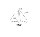
表示パネルにおける画素が、第1方向と第1方向に垂直な第2方向とに沿ってマトリクス配列されており、第1方向の画素ピッチが、第2方向の画素ピッチに比して大きくなっており、
上記バックライト光における第1方向の指向性が、第2方向での指向性よりも高くなっていることを特徴とする構成である。
本実施の形態にかかる液晶表示装置(本表示装置)は、携帯電話やPDA(personal digital assistant),デジタルカメラ,液晶モニター,液晶テレビジョン等の電子機器の表示画面に好適に応用することの可能な、直視型の半透過型液晶表示装置である。
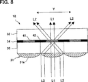
この図に示すように、本表示装置は、バックライト部11および液晶パネル12を備えている。
この図に示すように、液晶パネル12には、R(赤),G(緑),B(青)の画素41が、この図および図1に示すX方向に沿って周期的に並べられている。
tan-1(153(ピッチ)×1.52(ガラス屈折率)/2/300(基板厚))
=21°
となる。
ただし、バックライト部11から出射される光における指向性の小さい方向がY方向となるように、バックライト部11(あるいは光源)の配置を設定することが好ましい。
図16(a)〜(d)は、レンチキュラーレンズアレイ31の製造方法を説明するための断面図である。
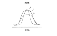
図17は、カラーフィルタ104R,104G,104Bの分光透過率特性を示すグラフである。なお、カラーフィルタ104R,104Gは、それぞれ、赤・緑のカラーフィルタである。この図に示すように、カラーフィルタ104R,104Gは、400nm近辺の光をほとんど透過しない。
なお、マイクロレンズアレイとは、規則正しく配列された複数のマイクロレンズ群のことである。
表示パネルにバックライト光を照射するとともに、表示パネルにマトリクス状に配列された複数の画素における光透過状態を制御することで画像を表示する表示装置において、
上記表示パネルが、画素に対応したマイクロレンズ群からなるマイクロレンズアレイを備えており、
表示パネルにおける画素が、第1方向と第1方向に垂直な第2方向とに沿ってマトリクス配列されており、第1方向の画素ピッチが、第2方向の画素ピッチに比して大きくなっており、
上記バックライト光における第1方向の指向性が、第2方向での指向性よりも高くなっていることを特徴とする構成である。
なお、レンチキュラーレンズを用いる場合、レンチキュラーレンズの集光方向を、上記の第1方向に向けることが好ましい。
θ=tan-1(D/(2×f))
また、通常、マイクロレンズアレイは、表示パネルのガラス基板に取り付けられている。このため、マイクロレンズを通過した光は、ガラス(屈折率n)中を通過することとなる。従って、この場合には、集光角は、
θ=tan-1(D・n/(2×f))
のように表される(この場合のfは、マイクロレンズのガラス中での焦点距離である)。
(a)表示パネルのバックライト側の面に、マイクロレンズの材料である感光性樹脂を塗布する工程
(b)表示パネルの画素を介して上記の感光性樹脂材料を露光する工程
(c)露光後の感光性樹脂材料を現像する工程。
これにより、出射強度の低下を、最大値(偏光交叉角が0°の場合)の数%程度と抑えられる。また、バックライト光の主偏光方向は、上記の第2方向に沿っていてもよい。
偏光回転素子を用いれば、バックライト光の主偏光方向を、任意の方向に回転させられる。従って、バックライト光の主偏光方向を、直線偏光板の透過軸の方向に近づけることが容易となる。
また、第3画像表示装置は、第1画像表示装置において、該光源が画像表示素子の複数色の画素の配列方向に対して、直交するする方向に配列されている構成である。例えば、文献3のサイドライト方式のバックライトは、光の伝播方向と、伝播方向に直交する方向とにおいて、出射光の指向性が異なる。
当然のことながら、ガラス基板厚が薄くなるとガラスの強度が低下し、液晶表示素子を作成するための工程内でのハンドリングの問題や、実使用下での外部からの衝撃に対する耐久性が得られなくなる。そこで、通常は文献1にも開示されているように、マイクロレンズの焦点位置が画素開口部よりも、マイクロレンズ側に来るようにマイクロレンズの焦点距離を設定することで、マイクロレンズの集光角だけを広げて、ガラス基板厚の薄型化を低減でき、指向性とガラス強度を両立させることができる。
また、第8画像表示装置は、RGB画素の配列方向とそれに直交する方向の両方向とも指向性の高いバックライトと、第1〜7画像表示装置のいずれかとを備えた構成である。携帯電話など、他人にディスプレイの情報を見られたくない場合は、本発明を適用すると、左右方向の指向性は狭いままで、上下方向だけの指向性が広げられるため、使用者自体は支障なくディスプレイが見られるが、隣からは、ディスプレイの内容が見えづらい。しかも、バックライトの全方位の指向性を高めているため、バックライト自体の正面輝度が更に上がり、高輝度のディスプレイが実現できる。
また、通常マイクロレンズの形成していない液晶パネルでは、ガラス基板表面に偏光板を貼ることができるが、マイクロレンズを形成した液晶パネルの場合、偏光板を貼ることが困難である。
よって、マイクロレンズ形成側の偏光板は、バックライト部11に使用されているプリズムシート24に貼り合わせてもよい。この場合、マイクロレンズ表面での反射が増えるが、プリズムシート表面での反射が減るため、表面反射による光ロスをキャンセルすることができる。
Claims (15)
- 表示パネルにバックライト光を照射するとともに、表示パネルにマトリクス状に配列された複数の画素における光透過状態を制御することで画像を表示する表示装置において、
上記表示パネルが、上記バックライト光の入射側にて、画素に対応したマイクロレンズ群からなるマイクロレンズアレイを備えており、
上記表示パネルにおける画素が、第1方向と第1方向に垂直な第2方向とに沿ってマトリクス配列されており、第1方向の画素ピッチが、第2方向の画素ピッチに比して大きくなっており、
上記マイクロレンズアレイに入射される前の上記バックライト光における第1方向の指向性が、第2方向での指向性よりも高くなっており、
上記マイクロレンズアレイにおける各マイクロレンズは、第1方向の集光角が第2方向の集光角よりも大きくなっていることを特徴とする表示装置。 - 上記バックライト光における第1方向での強度半値幅角が、±20°以下に設計されていることを特徴とする請求項1に記載の表示装置。
- 上記マイクロレンズが第1方向の光を集光するレンチキュラーレンズであることを特徴とする請求項1に記載の表示装置。
- 上記マイクロレンズにおける第1方向での集光角が、20°〜30°の範囲に設定されていることを特徴とする請求項1に記載の表示装置。
- 上記マイクロレンズが、液晶層の各画素と1:1対応した、第1方向および第2方向に集光力を有する微小レンズ群からなることを特徴とする請求項1に記載の表示装置。
- 上記マイクロレンズの焦点位置と表示パネルの画素とのずれが、マイクロレンズから画素までの距離の1/3以内の範囲に設定されていることを特徴とする請求項1に記載の表示装置。
- 上記マイクロレンズの焦点位置が、上記範囲内で画素よりもマイクロレンズ側に位置していることを特徴とする請求項6に記載の表示装置。
- 上記マイクロレンズが、以下の(a)〜(c)工程によって製造されることを特徴とする請求項1に記載の表示装置。
(a)表示パネルのバックライト側の面に、マイクロレンズの材料である感光性樹脂を塗布する工程
(b)表示パネルの画素開口部を介して上記の感光性樹脂材料を露光する工程
(c)露光後の感光性樹脂材料を現像する工程 - 上記表示パネルに直線偏光板が備えられているとともに、バックライト光が直線偏光性を有しており、
上記直線偏光板に入射される光の主偏光方向が、偏光板の透過軸に沿っていることを特徴とする請求項1に記載の表示装置。 - バックライト光の主偏光方向が、上記の第1方向に沿っていることを特徴とする請求項9に記載の表示装置。
- 上記直線偏光板の透過軸と直線偏光板に入射される光の主偏光方向とのなす角度である偏光交叉角が、±20°以内の範囲に設定されていることを特徴とする請求項9に記載の表示装置。
- 表示パネルとバックライトとの間に、上記偏光交叉角を上記の範囲に設定するための偏光回転素子を備えていることを特徴とする請求項11に記載の表示装置。
- 上記表示パネルにバックライト光を照射するバックライトの表示パネル側表面に、バックライトからの1方向に振動する直線偏光を透過させる偏光板が貼り合わされていることを特徴とする請求項1記載の表示装置。
- 上記表示パネルが、液晶パネルであることを特徴とする請求項1に記載の表示装置。
- 請求項14に記載の表示装置を備えたことを特徴とする電子機器。
Applications Claiming Priority (2)
| Application Number | Priority Date | Filing Date | Title |
|---|---|---|---|
| JP2004055215 | 2004-02-27 | ||
| PCT/JP2005/003679 WO2005083503A1 (en) | 2004-02-27 | 2005-02-25 | Display apparatus and electronic device |
Publications (2)
| Publication Number | Publication Date |
|---|---|
| JP2007522482A JP2007522482A (ja) | 2007-08-09 |
| JP4358230B2 true JP4358230B2 (ja) | 2009-11-04 |
Family
ID=34908855
Family Applications (1)
| Application Number | Title | Priority Date | Filing Date |
|---|---|---|---|
| JP2006524986A Expired - Fee Related JP4358230B2 (ja) | 2004-02-27 | 2005-02-25 | 表示装置および電子機器 |
Country Status (6)
| Country | Link |
|---|---|
| US (1) | US7715102B2 (ja) |
| JP (1) | JP4358230B2 (ja) |
| KR (1) | KR20060116033A (ja) |
| CN (1) | CN100517017C (ja) |
| TW (1) | TWI325076B (ja) |
| WO (1) | WO2005083503A1 (ja) |
Families Citing this family (33)
| Publication number | Priority date | Publication date | Assignee | Title |
|---|---|---|---|---|
| US20090322862A1 (en) * | 2006-08-31 | 2009-12-31 | Koninklijke Philips Electronics N.V. | Autostereoscopic display device |
| US8446339B2 (en) * | 2007-03-30 | 2013-05-21 | Pioneer Corporation | Image display device |
| TW200931130A (en) * | 2008-01-04 | 2009-07-16 | Univ Chung Yuan Christian | Structure for increasing the light usage ratio and luminance of display |
| US8094259B2 (en) * | 2008-04-16 | 2012-01-10 | Industry-Academic Cooperation Foundation, Yeungnam University | Liquid crystal display without color filter |
| US8477263B2 (en) * | 2008-05-20 | 2013-07-02 | Sharp Kabushiki Kaisha | Liquid crystal display device |
| CN102272667A (zh) * | 2009-01-09 | 2011-12-07 | 夏普株式会社 | 液晶显示装置和背光源 |
| CN102194851B (zh) * | 2010-03-17 | 2016-01-20 | 群创光电股份有限公司 | 影像显示系统 |
| TWI514916B (zh) * | 2010-03-17 | 2015-12-21 | Innolux Corp | 影像顯示系統 |
| KR20120045098A (ko) * | 2010-10-29 | 2012-05-09 | 삼성전자주식회사 | 백라이트 어셈블리 및 이를 갖는 액정 표시 장치 |
| JP2013025228A (ja) * | 2011-07-25 | 2013-02-04 | Stanley Electric Co Ltd | 立体表示装置 |
| TWI452554B (zh) * | 2012-02-29 | 2014-09-11 | Au Optronics Corp | 觸控面板、觸控顯示器及其組裝方法 |
| JP6260345B2 (ja) * | 2014-01-06 | 2018-01-17 | 株式会社Jvcケンウッド | 中間像形成部及びそれを用いた画像表示装置 |
| WO2016172709A1 (en) * | 2015-04-24 | 2016-10-27 | Tk Holdings Inc. | Steering wheel light bar |
| CN104867407B (zh) * | 2015-05-06 | 2020-09-29 | Tcl移动通信科技(宁波)有限公司 | 一种限定屏幕内容观看范围的移动终端及显示系统 |
| CN106959550B (zh) | 2016-01-08 | 2024-04-16 | 京东方科技集团股份有限公司 | 一种光学调制器、背光源模组及显示装置 |
| JP6299783B2 (ja) * | 2016-02-15 | 2018-03-28 | セイコーエプソン株式会社 | 電気光学装置、および電子機器 |
| CN105868742B (zh) * | 2016-05-26 | 2020-07-03 | 京东方科技集团股份有限公司 | 显示组件和显示装置 |
| CN105974671A (zh) * | 2016-07-25 | 2016-09-28 | 京东方科技集团股份有限公司 | 一种显示面板及制作方法 |
| JP7062366B2 (ja) | 2017-03-03 | 2022-05-06 | 株式会社ジャパンディスプレイ | 表示装置、表示方法及び色分離素子 |
| TWI626472B (zh) * | 2017-05-31 | 2018-06-11 | High efficiency head-up display illumination system using three primary color sources | |
| CN110133860B (zh) * | 2018-02-09 | 2022-01-25 | 中强光电股份有限公司 | 显示装置 |
| CN110133859B (zh) | 2018-02-09 | 2021-09-03 | 中强光电股份有限公司 | 显示装置 |
| TWI685700B (zh) * | 2018-08-14 | 2020-02-21 | 友達光電股份有限公司 | 顯示裝置與畫素結構 |
| CN109725480B (zh) * | 2019-02-27 | 2021-04-27 | 广西佳微科技股份有限公司 | 一种lcd投影装置及设计方法 |
| CN109839795B (zh) * | 2019-02-27 | 2021-04-09 | 广西佳微科技股份有限公司 | 一种小型投影模块 |
| CN110425491A (zh) * | 2019-08-01 | 2019-11-08 | 马瑞利汽车零部件(芜湖)有限公司 | 一种具有光幕效果的光学系统 |
| US10928669B1 (en) * | 2020-03-11 | 2021-02-23 | Shenzhen China Star Optoelectronics Semiconductor Display Technology Co., Ltd. | Display panel and display device |
| DE102020002323B3 (de) | 2020-04-07 | 2021-07-22 | Sioptica Gmbh | Optisches Element zur Beeinflussung von Lichtrichtungen und Bildschirm mit einem solchen optischen Element |
| CN111552108B (zh) * | 2020-06-08 | 2022-11-25 | 京东方科技集团股份有限公司 | 一种显示装置及其指纹识别方法 |
| CN112712754B (zh) * | 2020-12-31 | 2022-08-19 | 联想(北京)有限公司 | 显示装置以及电子设备 |
| CN112799158B (zh) * | 2021-01-27 | 2022-04-08 | 福州大学 | 一种基于光波导的类谐振腔光提取结构 |
| CN115291429B (zh) * | 2022-08-05 | 2023-07-25 | 武汉华星光电技术有限公司 | 一种液晶显示面板 |
| CN115407544B (zh) * | 2022-08-19 | 2024-04-16 | 京东方科技集团股份有限公司 | 反射式显示面板及显示装置 |
Family Cites Families (16)
| Publication number | Priority date | Publication date | Assignee | Title |
|---|---|---|---|---|
| US5101279A (en) * | 1989-12-14 | 1992-03-31 | Canon Kabushiki Kaisha | Liquid crystal display apparatus having lenticular elements oriented in relation to LC pixel aperture dimensions |
| JP2888358B2 (ja) * | 1989-12-14 | 1999-05-10 | キヤノン株式会社 | 液晶表示デバイス |
| JPH0596834U (ja) | 1992-05-29 | 1993-12-27 | 株式会社ケンウッド | 液晶プロジェクター |
| JPH07306399A (ja) * | 1994-05-13 | 1995-11-21 | Fujitsu Ltd | 液晶表示装置とその製造方法 |
| JP3289527B2 (ja) * | 1994-12-15 | 2002-06-10 | ソニー株式会社 | 液晶表示装置の製造方法 |
| JPH08313859A (ja) * | 1995-05-16 | 1996-11-29 | Hitachi Ltd | 液晶パネル、液晶投写型ディスプレイ、および立体投写型ディスプレイ |
| JP3900626B2 (ja) | 1997-11-10 | 2007-04-04 | 凸版印刷株式会社 | マイクロレンズ付きカラーフィルタ基板 |
| JP2000098296A (ja) * | 1998-09-17 | 2000-04-07 | Sharp Corp | 投影型カラー画像表示装置 |
| JP3293589B2 (ja) | 1999-04-13 | 2002-06-17 | 松下電器産業株式会社 | 液晶表示装置 |
| JP2000321431A (ja) * | 1999-05-17 | 2000-11-24 | Nitto Denko Corp | 偏光素子、光学素子、偏光光源装置及び液晶表示装置 |
| KR100806093B1 (ko) * | 2000-04-27 | 2008-02-21 | 가부시키가이샤 구라레 | 면광원소자 및 이를 사용한 표시장치 |
| JP2002062818A (ja) * | 2000-08-16 | 2002-02-28 | Sony Corp | マイクロレンズおよび画像表示装置の製造方法 |
| JP3710368B2 (ja) * | 2000-09-25 | 2005-10-26 | シャープ株式会社 | 積層フィルムの製造方法 |
| US6791639B2 (en) * | 2002-05-14 | 2004-09-14 | International Business Machines Corporation | Direct view display with lenticular lens for improved brightness and wide viewing angle |
| JP4040481B2 (ja) * | 2003-01-22 | 2008-01-30 | キヤノン株式会社 | 3次元構造形成方法 |
| US20060250707A1 (en) * | 2005-05-05 | 2006-11-09 | 3M Innovative Properties Company | Optical film having a surface with rounded pyramidal structures |
-
2005
- 2005-02-25 TW TW094105819A patent/TWI325076B/zh not_active IP Right Cessation
- 2005-02-25 CN CNB2005800060088A patent/CN100517017C/zh not_active Expired - Fee Related
- 2005-02-25 JP JP2006524986A patent/JP4358230B2/ja not_active Expired - Fee Related
- 2005-02-25 KR KR1020067019859A patent/KR20060116033A/ko not_active Application Discontinuation
- 2005-02-25 WO PCT/JP2005/003679 patent/WO2005083503A1/en active Application Filing
- 2005-02-25 US US10/590,825 patent/US7715102B2/en not_active Expired - Fee Related
Also Published As
| Publication number | Publication date |
|---|---|
| JP2007522482A (ja) | 2007-08-09 |
| TW200538817A (en) | 2005-12-01 |
| US7715102B2 (en) | 2010-05-11 |
| CN100517017C (zh) | 2009-07-22 |
| TWI325076B (en) | 2010-05-21 |
| CN1922539A (zh) | 2007-02-28 |
| US20070171493A1 (en) | 2007-07-26 |
| WO2005083503A1 (en) | 2005-09-09 |
| KR20060116033A (ko) | 2006-11-13 |
Similar Documents
| Publication | Publication Date | Title |
|---|---|---|
| JP4358230B2 (ja) | 表示装置および電子機器 | |
| TWI412832B (zh) | 彩色液晶顯示裝置組合 | |
| TWI317039B (en) | Display panel and manufacturing method thereof | |
| US7973880B2 (en) | Illumination device and liquid crystal display device | |
| JP3708112B2 (ja) | マイクロレンズアレイ付き表示パネルの製造方法および表示装置 | |
| US8111356B2 (en) | Liquid crystal display panel provided with microlens array, method for manufacturing the liquid crystal display panel, and liquid crystal display device | |
| TWI300493B (ja) | ||
| TWI239423B (en) | Display device | |
| US20100020263A1 (en) | Liquid crystal display panel provided with microlens array, method for manufacturing the liquid crystal display panel, and liquid crystal display device | |
| US20100007815A1 (en) | Liquid crystal display panel with microlens array, its manufacturing method, and liquid crystal display device | |
| WO2009141953A1 (ja) | 液晶表示装置 | |
| US20100085511A1 (en) | Display device | |
| WO2012043361A1 (ja) | 照明装置、及び表示装置 | |
| JP5434403B2 (ja) | 照明ユニット及び表示装置 | |
| JP2003029256A (ja) | 反射型表示装置、及び情報機器 | |
| JP2009222797A (ja) | 液晶表示パネル及び液晶表示装置 | |
| JP2007264640A (ja) | 表示パネルの製造方法 | |
| JP2000214528A (ja) | 表示装置 | |
| KR101101792B1 (ko) | 액정표시장치 및 조명장치 | |
| KR101374607B1 (ko) | 광학패턴층을 포함하는 액정표시장치와 패널 내 광학패턴층형성방법 | |
| KR100684027B1 (ko) | 액정표시장치 제조방법, 액정표시장치 및 이를 구비한이동통신 단말기 | |
| JP2005266820A (ja) | 露光装置およびそれを用いたマイクロレンズアレイを形成する方法 | |
| JP2009098541A (ja) | 表示装置及び表示装置の製造方法 | |
| JPH05143004A (ja) | 液晶表示装置 |
Legal Events
| Date | Code | Title | Description |
|---|---|---|---|
| A131 | Notification of reasons for refusal |
Free format text: JAPANESE INTERMEDIATE CODE: A131 Effective date: 20090324 |
|
| A521 | Request for written amendment filed |
Free format text: JAPANESE INTERMEDIATE CODE: A523 Effective date: 20090521 |
|
| TRDD | Decision of grant or rejection written | ||
| A01 | Written decision to grant a patent or to grant a registration (utility model) |
Free format text: JAPANESE INTERMEDIATE CODE: A01 Effective date: 20090804 |
|
| A01 | Written decision to grant a patent or to grant a registration (utility model) |
Free format text: JAPANESE INTERMEDIATE CODE: A01 |
|
| A61 | First payment of annual fees (during grant procedure) |
Free format text: JAPANESE INTERMEDIATE CODE: A61 Effective date: 20090805 |
|
| FPAY | Renewal fee payment (event date is renewal date of database) |
Free format text: PAYMENT UNTIL: 20120814 Year of fee payment: 3 |
|
| R150 | Certificate of patent or registration of utility model |
Free format text: JAPANESE INTERMEDIATE CODE: R150 |
|
| FPAY | Renewal fee payment (event date is renewal date of database) |
Free format text: PAYMENT UNTIL: 20120814 Year of fee payment: 3 |
|
| FPAY | Renewal fee payment (event date is renewal date of database) |
Free format text: PAYMENT UNTIL: 20130814 Year of fee payment: 4 |
|
| LAPS | Cancellation because of no payment of annual fees |