JP4340439B2 - Hall sensor with reduced offset signal - Google Patents
Hall sensor with reduced offset signal Download PDFInfo
- Publication number
- JP4340439B2 JP4340439B2 JP2002592700A JP2002592700A JP4340439B2 JP 4340439 B2 JP4340439 B2 JP 4340439B2 JP 2002592700 A JP2002592700 A JP 2002592700A JP 2002592700 A JP2002592700 A JP 2002592700A JP 4340439 B2 JP4340439 B2 JP 4340439B2
- Authority
- JP
- Japan
- Prior art keywords
- active region
- contact electrodes
- shape
- hall sensor
- contact
- Prior art date
- Legal status (The legal status is an assumption and is not a legal conclusion. Google has not performed a legal analysis and makes no representation as to the accuracy of the status listed.)
- Expired - Lifetime
Links
Images


Classifications
-
- G—PHYSICS
- G01—MEASURING; TESTING
- G01D—MEASURING NOT SPECIALLY ADAPTED FOR A SPECIFIC VARIABLE; ARRANGEMENTS FOR MEASURING TWO OR MORE VARIABLES NOT COVERED IN A SINGLE OTHER SUBCLASS; TARIFF METERING APPARATUS; MEASURING OR TESTING NOT OTHERWISE PROVIDED FOR
- G01D3/00—Indicating or recording apparatus with provision for the special purposes referred to in the subgroups
- G01D3/02—Indicating or recording apparatus with provision for the special purposes referred to in the subgroups with provision for altering or correcting the law of variation
-
- G—PHYSICS
- G01—MEASURING; TESTING
- G01D—MEASURING NOT SPECIALLY ADAPTED FOR A SPECIFIC VARIABLE; ARRANGEMENTS FOR MEASURING TWO OR MORE VARIABLES NOT COVERED IN A SINGLE OTHER SUBCLASS; TARIFF METERING APPARATUS; MEASURING OR TESTING NOT OTHERWISE PROVIDED FOR
- G01D5/00—Mechanical means for transferring the output of a sensing member; Means for converting the output of a sensing member to another variable where the form or nature of the sensing member does not constrain the means for converting; Transducers not specially adapted for a specific variable
- G01D5/12—Mechanical means for transferring the output of a sensing member; Means for converting the output of a sensing member to another variable where the form or nature of the sensing member does not constrain the means for converting; Transducers not specially adapted for a specific variable using electric or magnetic means
- G01D5/14—Mechanical means for transferring the output of a sensing member; Means for converting the output of a sensing member to another variable where the form or nature of the sensing member does not constrain the means for converting; Transducers not specially adapted for a specific variable using electric or magnetic means influencing the magnitude of a current or voltage
- G01D5/142—Mechanical means for transferring the output of a sensing member; Means for converting the output of a sensing member to another variable where the form or nature of the sensing member does not constrain the means for converting; Transducers not specially adapted for a specific variable using electric or magnetic means influencing the magnitude of a current or voltage using Hall-effect devices
-
- H—ELECTRICITY
- H10—SEMICONDUCTOR DEVICES; ELECTRIC SOLID-STATE DEVICES NOT OTHERWISE PROVIDED FOR
- H10N—ELECTRIC SOLID-STATE DEVICES NOT OTHERWISE PROVIDED FOR
- H10N52/00—Hall-effect devices
- H10N52/101—Semiconductor Hall-effect devices
-
- H—ELECTRICITY
- H10—SEMICONDUCTOR DEVICES; ELECTRIC SOLID-STATE DEVICES NOT OTHERWISE PROVIDED FOR
- H10N—ELECTRIC SOLID-STATE DEVICES NOT OTHERWISE PROVIDED FOR
- H10N52/00—Hall-effect devices
- H10N52/80—Constructional details
Abstract
Description
【0001】
本発明はホール・センサに関し、さらに詳しくは、オフセット信号の低減のために改善されたコンタクト電極形状をもち、CMOS技術で実現されたホール・センサに関する。
【0002】
一般的に、ホール・センサは、pドープ半導体基板上のnドープ活性半導体領域から構成される。通常、nドープ活性領域は、活性領域に対角線方向に相対して配置された4つのコンタクト電極を介して外部制御ロジックに接続される。4つのコンタクト電極は、活性領域に電流を発生させるために設けられた2つの相対する制御電流コンタクト電極と、印加磁場の存在時に活性領域内の電流に垂直に発生するセンサ信号としてのホール電圧をタップオフ(tap-off)するために設けられた2つの対向する電圧タップ・コンタクト電極に分けられる。
【0003】
通常、上述した構成を持つホール・センサでは、活性センサ領域について、図5及び6に示される2つの既知の形状がある。図5は方形のホール・センサ20を示し、そのコンタクト電極22a−dは活性領域24の隅にそれぞれ配置されている。この既知のホール・センサ構成をもつホール・センサのコンタクト電極22a−dの形状は通常、方形である。このホール・センサ20の動作中、対角線方向に相対する2つのコンタクト電極22a、22c間には、印加磁場の存在時に他の2つのコンタクト電極22b、22d間でホール電圧をタップオフできるように電流が供給される。
【0004】
図6は「ギリシャ十字」の形状の十字形ホール・センサ構成30を示し、そこでは矩形のコンタクト電極32a−dが十字アームの端部にそれぞれ存在し、コンタクト電極32a−dの後部境界が活性領域34の境界と一致している。コンタクト電極32a−dの幅は十字アームの幅と一致する。つまり、コンタクト電極32a−dは、それぞれの十字アームにおいて活性領域34の全幅にわたって伸長する。方形のホール・センサと同様に、十字形ホール・センサの動作中、2つの相対するコンタクト電極32a、32c間には、印加磁場の存在時に2つのコンタクト電極32b、32d間でホール電圧をタップオフできるように電流が供給される。
【0005】
しかし、半導体構造を製造するためのCMOSプロセスでは、製造工程のために活性領域の半導体材料に異質物又は欠陥がしばしば発生する。これらの異質物は、高価な製造方法を用いても完全には回避できない。しかし、これらの異質物は、センサ信号のオフセット発生の原因であることがよくある。これは、磁場が活性領域に印加されないときでも、ホール電圧がタップオフされるコンタクト電極にセンサ信号が検出されることを意味する。この妨害センサ信号は、有効センサ信号オフセット又は単にオフセット信号と呼ばれる。これらの異質物が活性領域の不都合な位置にある場合、既知のホール・センサ素子では、活性領域の電流線が不都合に変化し、結果として活性領域における局所的な高抵抗となりうるので、比較的高いオフセット信号が存在し得る。そのため、ホール・センサ素子に発生するセンサ信号のオフセットは、異質物の数及びそれらの異質物の位置に強く依存する。
【0006】
従来のホール・センサ素子における異質物に対するオフセット信号のこの強い依存性のため、大きい典型的変動が発生する。さらに、ホール・センサの感度及び測定精度が強く影響を受ける。この理由から、センサ信号のオフセット補償及び正確な評価は一般的に、非常に高価な回路技術を必要とする。
【0007】
この先行技術から出発して、センサ信号におけるオフセットを低減した改善ホール・センサ素子を提供することが本発明の目的である。
【0008】
この目的は、請求項1に記載のホール・センサ素子によって達成される。
【0009】
本発明は、2つの相対する電力供給コンタクト電極とそれらの間に画定された活性領域をもってその活性領域に電流を発生させるとともに、ホール電圧をタップオフするための2つの相対する電圧タップ・コンタクト電極を持つホール・センサ素子であって、それぞれのコンタクト電極で活性領域に面する部分が、スピン電流作用のオフセット低減効果に対するコンタクト電極の妨害作用を低減するような仕方で形成されていることを特徴とするホール・センサ素子を提供する。
【0010】
本発明は、ホール・センサ素子で発生するセンサ信号のオフセットが、使用されるコンタクト電極の形状の適切な選択によって強く低減できるという認識に基づいている。すなわち、センサ信号のオフセットを小さくするためには、従来のセンサ構造が主に前提としているような、半導体材料の理想的な状態、つまり異質物のない状態における制御電流の均質な電流密度分布だけが重要なのではなく、活性領域の半導体材料及び、特にコンタクトにおけるこの異質物又は妨害のために電流密度分布がいかに変化するかがはるかに重要である。結果として起こるオフセット値の変動を低く維持するためには、やはり、センサ信号のオフセットは半導体材料における異質物又は妨害の位置にできるだけ無関係でなければならない。
【0011】
本発明による形状の利点は以下の文脈に基づいている。ホール素子の外部から測定可能なオフセットは、次の3つの基本的要素に依存する。
− 素子における効果の強度及び広がり
− 素子の動作電圧
− 素子の形状
【0012】
最初の2つの要素はこの文脈ではこれ以上考慮しない。この場合、変化のために残されるのは形状だけである。形状は、素子の特性に対して広大かつ多様な影響を持つ。コンタクトの形状と以下で説明するスピン電流によって低減される素子のオフセットとの間には、特別な関係が存在する。
【0013】
スピン電流法は、測定方向が絶えず周期的に、特定のクロック周波数で例えば90°だけ回転する、つまり、1つのコンタクト電極から相対するコンタクト電極に動作電流が流れ、そこでホール電圧が対角線方向に相対するコンタクト電極でタップオフされ、それにより次のサイクルでは測定方向が90°回転する、という事実から成る。測定されたホール電圧は加算されてオフセット電圧は1サイクル内で相互にほとんど相殺されるはずであり、信号のうち真に磁場に依存する部分が残されるようになる。
【0014】
スピン電流無しの動作時でも、選択された素子及びコンタクト形状によって、影響が障害とならない位置と、それらが大きいオフセットを生じる位置が生じる。良い例は、2つの制御電流コンタクト間の接続線である。対称性のため、この接続線上の欠陥はオフセットにつながらない。しかし、この線からわずかに逸脱するや否や、両方の点における電流密度がほぼ同一でありかつ無視できるほどには小さくないにもかかわらず、ただちにホール・コンタクトに測定可能なオフセットが生じる。
【0015】
スピン電流で動作中には、形状によって、オフセットに対する特定の位置における欠陥の効果を説明する感度関数が場所全体に生じる。有限延長制御又はホール・コンタクトの場合、この関数は比較的複雑のように見える。通常のホール・クロス(hall cross)では、この関数はそれぞれ相対するコンタクト間、及びさらにクロスの内部領域の二等分線間を結ぶ接続線上に零点を持つ。残りの輪郭線、及びそれによって特に活性領域におけるこの関数の極値は、素子及びコンタクトの形状の適切な選択によって影響を受けることがあり得る。通常、オフセットに高い関連性がある場所は素子及びコンタクトの縁にあり、一方内部領域は通常新しい局所的極値を持たない。形状の変形により素子の全ての他の特性もまた変化し得るので、コンタクトの変化のために全ての他の特性について考慮する必要がある。
【0016】
本発明によるコンタクトでは、高い歩留まり及びほとんど変化しない感度で低いオフセットが達成できるような方法で、形状が形成された。
【0017】
実効的な解像度は、それ故、素子の低オフセットにより増加する。
【0018】
本発明の好適な実施形態を添付の図面を参照しながら以下にさらに詳しく説明する。
【0019】
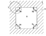
図1を参照すると、矩形ホール・センサ素子1の一般構成が示されている。好ましくはpドープされた半導体基板3上に、通常nドープされた矩形活性半導体領域5が配置されている。nドープ活性領域5の隅に近接して、通常n+ドーピングによって得られるコンタクト電極7a−dが配置されている。コンタクト電極7a−dは、pドープ基板によって包囲されたnドープ活性領域5内にそれぞれ対角線方向に相対して配置されている。コンタクト電極7a−dで活性領域5に面する部分の点線で示した輪郭は、各々以下で図2a−fを参照しながら詳細に説明するコンタクト電極7a−dのさらに異なる新しい構造を示すものである。
【0020】
図2a−eでは、コンタクト電極7a−dの様々な好適な形状が示されている。他のコンタクト電極7b−dは通常同一構造を持ち、かつ活性領域5の他の隅に対称的に配置されているので、以下の説明を簡潔にするために、一定の比率で拡大され、コンタクト構造7aが配置されたホール・センサ素子1の1つの隅領域(図1のセクションIの破線の円を参照)だけが示されている。説明を簡潔にするために、図2a−eに示すコンタクト電極7a−dははっきりと2つの部分、つまり1つは活性領域5に面する部分、及び1つは活性領域5から離れる方を向いた部分に分けられる。さらに、コンタクト電極7a−dの本発明の構造がその間に存在する2つの端点A及びBがコンタクト電極7a−dに定義されている。
【0021】
図2aの実施形態では、コンタクト電極7aで活性領域5に面する部分は直線として形成されているので、コンタクト電極7aは二等辺三角形の形状に形成されている。
【0022】
図2bはコンタクト電極7aの構造についての一実施形態を示しており、そこではコンタクト電極7aで活性領域に面する部分の端点A、Bが階段状又はステップ状に接続され、図2bに示されるコンタクト電極形状の階段状又はステップ状輪郭が形成されている。
【0023】
図2cは、活性領域に向かって湾曲した、端点A、B間の弓形構造を有するコンタクト電極形状を示している。コンタクト電極のこの湾曲構造はまた楕円形、放物線形、又は双曲線形の輪郭をとることもできる。
【0024】
図2dには、コンタクト電極7aで活性領域に面する部分が二等辺台形の形状を持ち、台形の長い底辺がコンタクト電極形状の端点A及びB間を通るコンタクト電極形状が示されている。
【0025】
図2eには、活性領域5に面する台形の短い底辺が、活性領域の方向に湾曲した弓形、楕円形、放物線形、又は双曲線形の輪郭を有するという点で、図2dの構造に比べてさらに発展したコンタクト電極7aの構造が示されている。
【0026】
上述のコンタクト電極形状は、厳密な数学的記述のために多角形の列(polygon train)によって近似することもできる。
【0027】
オフセット信号が著しく低減したホール・センサの最適動作特性を得るためには、つまり、ホール・センサの活性領域における電流密度分布が半導体材料内の異質物又は欠陥の位置にほとんど無関係になるようにするためには、コンタクト電極の横の長さは、活性領域の横の長さのせいぜい20%とすべきであることも明らかになった。
【0028】
さらに、コンタクト電極7a−dで活性領域から離れる方向を向いた部分の構造が、図2a−fに示されるような三角形の輪郭に限定されず、それぞれの適用の事例、例えば外部と接触するのに、又はコンタクト電極にリードを付けるのに適した形状を持つことができることに注意されたい。コンタクト電極7a−dで活性領域から離れる方向を向いた部分の輪郭は、本発明の主題にとって本質的なものではない。
【0029】
ホール・センサ素子のコンタクト電極の上述の新しい構造により、例えば活性領域の半導体材料に製造時に生じた異質物のために発生し、ホール電圧信号と重なる、好ましくないオフセット信号は低減することができる。この改善は、生じるオフセット信号が半導体材料の異質物又は欠陥の位置にほとんど無関係になるような本発明のコンタクト電極構造によって達成される。それによって、典型的変動を低減することができ、上述の新規なコンタクト構造を使用したホール・センサ素子の測定精度を改善することができる。
【0030】
図3aを参照すると、十字形ホール・センサ素子10の一般構成が示されている。好ましくはpドープされた半導体基板13上に、通常nドープされた十字形活性半導体領域15が配置されている。活性領域15の十字アームの端の近くに、一般にn+クラスのドーピングによって得られるコンタクト電極17a−dが配置されている。ホール・センサ素子内に電流を発生させるため、及び印加磁場の存在時に発生するホール電圧をタップオフするために設けられたそれぞれのコンタクト電極17a−dが、十字アームに対称的に相対して配置されている。コンタクト電極で活性領域に面する部分の点線で示した曲線は、図1に対応し、以下に図4a−gを参照しながら詳細に説明するコンタクト電極17a−dのさらに異なる新しい構造を示すものである。
【0031】
当然、内側に突出した素子の隅が図3b−dに示す例によって変化した変形十字素子を使用することができる。それ故、図3dは方形素子との境界の事例と見ることができる。
【0032】
コンタクト電極17a−dの様々な好適な形状を図4a−gに示す。他のコンタクト電極17b−dは同一構造を持ち、かつ活性領域15の他の十字アームに対称的に配置されるので、以下の説明を簡潔にするために、図4a−gではホール・センサ素子10のコンタクト電極17aが配置された1つの十字アームだけを示す(図3aのセクションIIの点線の円を参照)。説明を簡潔にするために、図4a−gに示されたコンタクト電極ははっきりと2つの部分、つまり活性領域に面する部分と活性領域から離れる方を向いた部分に分けられている。さらに、コンタクト電極17a−dの本発明による構造がその間に存在する2つの端点C及びDが再び定義されている。
【0033】
図4aに示す最も簡単な例では、コンタクト電極17aの形状は矩形の輪郭を持ち、コンタクト電極17aはnドープ材料によって完全に包囲されている。
【0034】
図4bには、コンタクト電極17aで活性領域15に面する部分のさらに可能な輪郭が示されている。この輪郭は、端点C、D間の矩形の延長として形成されている。
【0035】
図4cは、コンタクト電極17aが端点C、D間に活性領域に向かって湾曲した弓形の輪郭を有するコンタクト電極形状を示す。輪郭はさらに楕円、放物線形、又は双曲線形とすることができる。
【0036】
コンタクト電極17aで活性領域に面する部分の形状はさらに、図4dに示されるように、台形の長い底辺が端点CとD間の仮想接続線と一致する台形の輪郭をとることができる。
【0037】
図4eには、台形の短い底辺が活性領域の方向に湾曲した弓形、楕円形、放物線形状、又は双曲線形状の輪郭を持つように、図4dに示された構造に比べてさらに発展したコンタクト電極17aの構造が示されている。
【0038】
図4a−gに示されているように、コンタクト電極の形状のさらなる構造は、コンタクト電極で活性領域から離れる方向を向いた部分が少なくとも部分的にpドープ基板領域まで伸長するものとすることができる。そのような構造の1つの実施形態は図4fに例示的に示されている。しかし、この例で示されている端点C、D間のコンタクト構造17aの弓形の輪郭は、図4a−eに示されている全ての他のコンタクト電極の曲線を持つこともできる。
【0039】
さらに、コンタクト電極で活性領域から離れる方向を向いた部分全体を、図4gに示されるようにp基板に隣接して配置することができ、この場合、コンタクト電極の幅は十字アームの活性領域の幅と一致する。つまり、コンタクト電極17aは十字アームの全幅にわたって伸長する。コンタクト電極17aで活性領域に面する部分については、図4b−eに示された、活性領域15に向かって湾曲した曲線を持つことができる。
【0040】
また、上述のコンタクト電極構造は、活性領域が十字形の構造を持つホール・センサ素子で使用できるだけでなく、これらの構造は活性領域が星形の輪郭を有するホール・センサ素子でも使用できることに注意されたい。
【0041】
矩形活性領域について図2a−eにより説明されたコンタクト構造及び十字形活性領域について図4a−gにより説明されたコンタクト構造の両方に関して、それらが完全にnドープ領域内に置かれ、外部とは金属化層を介して接続されるだけとすることができることにも注意されたい。その結果、コンタクト領域はnドープ半導体領域によって完全に包囲される。それとは別に、例えば図4gに示されるように、コンタクト電極を完全に活性半導体領域内に置かない可能性もある。これは、コンタクト電極で活性領域から離れる方向を向いた部分の少なくとも境界が、活性領域の境界と接することができることを意味する。
【0042】
さらに、電流供給用のコンタクト電極(7a、7c;17a、17c)及び電圧タップ用のコンタクト電極(7b、7d;17b、17d)は同一形状を持ち、オフセット補償のためにいわゆる「スピン電流」法を有利に利用することが可能であることに注意されたい。本発明により設計されたコンタクトの利点は、スピン電流法で特に顕著である。
【0043】
従来のコンタクト電極構造を持つホール・センサでは、半導体材料の異質物のために発生するオフセット電圧が活性領域内の異なる各電流方向に対して異なる値を持つので、上述の補償方法を使用した場合でも、満足なオフセット抑制を達成することができない。
【0044】
それに対し、本発明によるコンタクト電極構造を使用すると、発明によるコンタクトによってスピン電流作用のオフセット低減効果が妨害される程度は、通常のコンタクト形状と比較してはるかに低いので、ほぼ完全なオフセット補償を期待することができる。
【図面の簡単な説明】
【図1】 本発明によるコンタクト電極を持つ方形ホール・センサ素子の概略図である。
【図2】 a−eは方形ホール・センサ素子に対する本発明によるコンタクト電極の種々の構造の概略図である。
【図3】 aは本発明によるコンタクト電極を持つ十字形ホール・センサ素子の概略図である。b−dはその十字構造の変形例である。
【図4】 a−gは十字形ホール・センサ素子に対する本発明によるコンタクト電極の種々の構造の概略図である。
【図5】 方形活性領域及び従来のコンタクト電極を持つ既知のホール・センサ素子である。
【図6】 十字形活性領域及び従来のコンタクト電極を持つ既知のホール・センサ素子である。[0001]
The present invention relates to a Hall sensor, and more particularly, to a Hall sensor implemented with CMOS technology having an improved contact electrode shape for reducing offset signals.
[0002]
In general, a Hall sensor is composed of an n-doped active semiconductor region on a p-doped semiconductor substrate. Usually, the n-doped active region is connected to external control logic via four contact electrodes arranged diagonally relative to the active region. The four contact electrodes have two opposing control current contact electrodes provided for generating a current in the active region and a Hall voltage as a sensor signal generated perpendicular to the current in the active region in the presence of an applied magnetic field. It is divided into two opposing voltage tap contact electrodes provided for tap-off.
[0003]
Typically, in a Hall sensor having the configuration described above, there are two known shapes for the active sensor region shown in FIGS. FIG. 5 shows a
[0004]
FIG. 6 shows a cross-shaped
[0005]
However, in a CMOS process for manufacturing a semiconductor structure, foreign materials or defects are often generated in the semiconductor material in the active region due to the manufacturing process. These foreign substances cannot be completely avoided even by using an expensive manufacturing method. However, these extraneous materials are often the cause of sensor signal offsets. This means that even when no magnetic field is applied to the active region, a sensor signal is detected at the contact electrode where the Hall voltage is tapped off. This disturbing sensor signal is referred to as a valid sensor signal offset or simply an offset signal. If these extraneous materials are at an inconvenient location in the active region, the known Hall sensor element can have an inconsequential change in the current line in the active region, resulting in local high resistance in the active region. There may be a high offset signal. Therefore, the offset of the sensor signal generated in the Hall sensor element strongly depends on the number of foreign objects and the positions of those foreign objects.
[0006]
Due to this strong dependence of the offset signal on foreign matter in conventional Hall sensor elements, large typical variations occur. Furthermore, the sensitivity and measurement accuracy of the Hall sensor are strongly affected. For this reason, offset compensation and accurate evaluation of sensor signals generally requires very expensive circuit technology.
[0007]
Starting from this prior art, it is an object of the present invention to provide an improved Hall sensor element with reduced offset in the sensor signal.
[0008]
This object is achieved by a Hall sensor element according to claim 1.
[0009]
The present invention has two opposing voltage-tap contact electrodes for generating current in the active region with two opposing power supply contact electrodes and an active region defined therebetween, and for tapping off the Hall voltage. Hall sensor element having each contact electrode facing the active region is formed in such a way as to reduce the interference effect of the contact electrode against the effect of reducing the offset of the spin current effect A hall sensor element is provided.
[0010]
The present invention is based on the recognition that the offset of the sensor signal generated in the Hall sensor element can be strongly reduced by an appropriate selection of the shape of the contact electrode used. In other words, in order to reduce the offset of the sensor signal, only the homogeneous current density distribution of the control current in the ideal state of the semiconductor material, that is, in the state of no foreign matter, as the main premise of the conventional sensor structure It is much more important that how the current density distribution changes due to this foreign material or interference in the active region semiconductor material and especially in the contacts. Again, in order to keep the resulting offset value variation low, the offset of the sensor signal must be as independent as possible of the location of the foreign or obstruction in the semiconductor material.
[0011]
The advantages of the shape according to the invention are based on the following context. The offset measurable from the outside of the Hall element depends on the following three basic factors.
− Intensity and spread of the effect in the device − Operating voltage of the device − Shape of the device
The first two factors are not considered further in this context. In this case, only the shape is left for change. The shape has a vast and varied influence on the device characteristics. There is a special relationship between the shape of the contact and the offset of the device that is reduced by the spin current described below.
[0013]
In the spin current method, the measurement direction is continuously and periodically rotated by, for example, 90 ° at a specific clock frequency, that is, an operating current flows from one contact electrode to the opposite contact electrode, where the Hall voltage is relative to the diagonal direction. Consists of the fact that the measuring direction is rotated 90 ° in the next cycle, thereby tapping off at the contact electrode. The measured Hall voltages are added together so that the offset voltages should almost cancel each other out in one cycle, leaving a truly magnetic field dependent portion of the signal.
[0014]
Even in the operation without spin current, the position where the influence does not become an obstacle and the position where they cause a large offset occur depending on the selected element and the contact shape. A good example is a connection line between two control current contacts. Due to symmetry, defects on this connecting line do not lead to an offset. However, as soon as it deviates slightly from this line, there is an immediately measurable offset in the Hall contact, even though the current density at both points is approximately the same and not negligibly small.
[0015]
When operating with spin current, the shape creates a sensitivity function across the location that accounts for the effect of the defect at a particular location on the offset. For finite extension control or hole contact, this function appears to be relatively complex. In a normal hall cross, this function has zeros on the connecting lines that connect each other between the contacts, and also between the bisectors of the interior region of the cross. The remaining contours, and thereby the extreme values of this function, particularly in the active region, can be affected by appropriate selection of element and contact shapes. Typically, locations that are highly related to offset are at the edge of the element and contacts, while the internal regions usually do not have new local extremes. Since all other characteristics of the device can also change due to shape deformation, all other characteristics need to be considered for contact changes.
[0016]
In the contact according to the invention, the shape was formed in such a way that a low offset could be achieved with a high yield and a sensitivity that hardly changed.
[0017]
The effective resolution is therefore increased due to the low offset of the element.
[0018]
Preferred embodiments of the present invention will be described in more detail below with reference to the accompanying drawings.
[0019]
Referring to FIG. 1, the general configuration of a rectangular Hall sensor element 1 is shown. A normally n-doped rectangular
[0020]
In FIGS. 2a-e, various suitable shapes of the
[0021]
In the embodiment of FIG. 2a, since the portion of the
[0022]
FIG. 2b shows an embodiment of the structure of the
[0023]
FIG. 2c shows a contact electrode shape having an arcuate structure between end points A and B, curved towards the active region. This curved structure of the contact electrode can also have an elliptical, parabolic or hyperbolic contour.
[0024]
FIG. 2d shows a contact electrode shape in which the portion of the
[0025]
In FIG. 2e, the short base of the trapezoid facing the
[0026]
The contact electrode shape described above can also be approximated by a polygon train for a precise mathematical description.
[0027]
To obtain the optimum operating characteristics of a Hall sensor with significantly reduced offset signals, that is, to make the current density distribution in the active area of the Hall sensor almost independent of the location of foreign objects or defects in the semiconductor material. the, the horizontal length of the contact electrode is also revealed that it should at most 20% of the horizontal length of the active region for.
[0028]
Furthermore, the structure of the part of the
[0029]
Due to the above-described new structure of the contact electrode of the Hall sensor element, an undesirable offset signal that is generated due to, for example, foreign material generated in the semiconductor material in the active region and overlaps with the Hall voltage signal can be reduced. This improvement is achieved by the contact electrode structure of the present invention in which the resulting offset signal is largely independent of the location of foreign material or defects in the semiconductor material. Thereby, typical fluctuations can be reduced and the measurement accuracy of the Hall sensor element using the novel contact structure described above can be improved.
[0030]
Referring to FIG. 3a, the general configuration of the cross-shaped
[0031]
Naturally, it is possible to use a deformed cross element in which the corners of the element protruding inward are changed according to the example shown in FIGS. 3b-d. Therefore, FIG. 3d can be seen as an example of a boundary with a square element.
[0032]
Various suitable shapes for the
[0033]
In the simplest example shown in FIG. 4a, the shape of the
[0034]
FIG. 4 b shows a further possible contour of the part of the
[0035]
FIG. 4 c shows a contact electrode shape in which the
[0036]
The shape of the portion of the
[0037]
FIG. 4e shows a further developed contact electrode compared to the structure shown in FIG. 4d so that the short base of the trapezoid has an arcuate , elliptical, parabolic or hyperbolic profile curved in the direction of the active region. The structure of 17a is shown.
[0038]
As shown in FIGS. 4a-g, a further structure in the shape of the contact electrode may be such that the portion of the contact electrode facing away from the active region extends at least partially to the p-doped substrate region. it can. One embodiment of such a structure is exemplarily shown in FIG. 4f. However, the arcuate contour of the
[0039]
Furthermore, the entire portion of the contact electrode facing away from the active region can be placed adjacent to the p substrate as shown in FIG. 4g, in which case the width of the contact electrode is the width of the active region of the cross arm. Matches the width. That is, the
[0040]
In addition, the above-mentioned contact electrode structure can be used not only for Hall sensor elements whose active regions have a cruciform structure, but these structures can also be used for Hall sensor elements whose active regions have a star-shaped contour. I want to be.
[0041]
For both the contact structure described by FIGS. 2a-e for the rectangular active region and the contact structure described by FIGS. 4a-g for the cruciform active region, they are placed completely within the n-doped region, the outside being metal Note also that it can only be connected through a layer. As a result, the contact region is completely surrounded by the n-doped semiconductor region. Alternatively, the contact electrode may not be completely in the active semiconductor region, for example as shown in FIG. 4g . This means that at least the boundary of the portion of the contact electrode facing away from the active region can be in contact with the boundary of the active region.
[0042]
Further, the current supply contact electrodes (7a, 7c; 17a, 17c) and the voltage tap contact electrodes (7b, 7d; 17b, 17d) have the same shape, and the so-called “spin current” method is used for offset compensation. Note that can be used to advantage. The advantages of contacts designed according to the present invention are particularly pronounced with the spin current method.
[0043]
In the Hall sensor having a conventional contact electrode structure, the offset voltage generated due to the foreign material of the semiconductor material has different values for different current directions in the active region. However, satisfactory offset suppression cannot be achieved.
[0044]
On the other hand, when the contact electrode structure according to the present invention is used, the contact reduction effect of the spin current action is much less disturbed by the contact according to the present invention than the normal contact shape, so that almost complete offset compensation is achieved. You can expect.
[Brief description of the drawings]
FIG. 1 is a schematic diagram of a square Hall sensor element with contact electrodes according to the present invention.
FIGS. 2a to 2e are schematic views of various structures of contact electrodes according to the invention for square Hall sensor elements. FIGS.
FIG. 3a is a schematic view of a cross-shaped Hall sensor element having a contact electrode according to the present invention. bd is a modification of the cross structure.
FIGS. 4a to 4g are schematic views of various structures of contact electrodes according to the present invention for cruciform Hall sensor elements. FIGS.
FIG. 5 is a known Hall sensor element with a square active region and a conventional contact electrode.
FIG. 6 is a known Hall sensor element with a cruciform active region and a conventional contact electrode.
Claims (3)
スピン電流作用のオフセット低減効果に対する前記2つの相対する電流供給コンタクト電極(7a,7c;17a,17c)間の前記活性領域(5,15)における不均質さに起因する妨害作用を低減するために、前記コンタクト電極(7a−7d;17a−17d)で前記活性領域(5;15)に面しかつ前記活性領域(5、15)に隣接する部分が前記活性領域(5,15)に向かって凸状に湾曲する形状で、かつ弓形、楕円形、放物線形、又は双曲線形を持ち、
前記コンタクト電極(7a−7d;17a−17d)が同一形状を持ち、それぞれ前記活性領域(5;15)に関して対称的に配置され、
かつ、前記コンタクト電極(7a−7d;17a−17d)のうちの前記活性領域(5;15)に面する前記部分の長さが前記2つの相対する電流供給コンタクト電極間の前記活性領域(5,15)の長さのせいぜい20%であることを特徴とするホール・センサ素子(1;10)。 An n-doped active region (5; 15) and four n + doped contact electrodes (7a-7d; 17a-17d) are provided, the contact electrodes (7a-7d; 17a-17d) being interposed between the active regions (5 15) are defined and two opposing current supply contact electrodes (7a, 7c; 17a, 17c) for generating a current in the active region (5, 15), and 2 for tapping off the Hall voltage In the Hall sensor element (1; 10) formed by two opposing voltage tap contact electrodes (7b, 7d; 17b, 17d),
To reduce the disturbing effect due to the inhomogeneity in the active region (5, 15) between the two opposing current supply contact electrodes (7a, 7c; 17a, 17c) against the offset reduction effect of the spin current action A portion of the contact electrode (7a-7d; 17a-17d) facing the active region (5; 15) and adjacent to the active region (5, 15) is directed toward the active region (5, 15). It has a convexly curved shape and has an arcuate shape, an elliptical shape, a parabolic shape, or a hyperbolic shape,
The contact electrodes (7a-7d; 17a-17d) have the same shape and are arranged symmetrically with respect to the active region (5; 15), respectively;
The length of the portion of the contact electrode (7a-7d; 17a-17d) facing the active region (5; 15) is the active region (5) between the two current supply contact electrodes facing each other. , 15) at most 20% of the length of the sensor element (1; 10).
Applications Claiming Priority (2)
| Application Number | Priority Date | Filing Date | Title |
|---|---|---|---|
| DE19908473A DE19908473B4 (en) | 1999-02-26 | 1999-02-26 | Hall sensor with reduced offset signal |
| PCT/EP2000/000313 WO2000052424A1 (en) | 1999-02-26 | 2000-01-17 | Hall sensor with a reduced offset signal |
Publications (2)
| Publication Number | Publication Date |
|---|---|
| JP2004519870A JP2004519870A (en) | 2004-07-02 |
| JP4340439B2 true JP4340439B2 (en) | 2009-10-07 |
Family
ID=7899039
Family Applications (1)
| Application Number | Title | Priority Date | Filing Date |
|---|---|---|---|
| JP2002592700A Expired - Lifetime JP4340439B2 (en) | 1999-02-26 | 2000-01-17 | Hall sensor with reduced offset signal |
Country Status (13)
| Country | Link |
|---|---|
| US (1) | US6639290B1 (en) |
| EP (1) | EP1155287B1 (en) |
| JP (1) | JP4340439B2 (en) |
| AT (1) | ATE224040T1 (en) |
| CA (1) | CA2363504C (en) |
| CZ (1) | CZ301988B6 (en) |
| DE (2) | DE19908473B4 (en) |
| DK (1) | DK1155287T3 (en) |
| ES (1) | ES2179808T3 (en) |
| HU (1) | HU229006B1 (en) |
| PL (1) | PL193791B1 (en) |
| PT (1) | PT1155287E (en) |
| WO (1) | WO2000052424A1 (en) |
Families Citing this family (23)
| Publication number | Priority date | Publication date | Assignee | Title |
|---|---|---|---|---|
| DE10158836B4 (en) * | 2001-11-30 | 2007-06-06 | Infineon Technologies Ag | Method and device for calibrating a sensor system |
| DE10244096B4 (en) * | 2002-09-23 | 2015-05-28 | Robert Bosch Gmbh | Spinning current Hall sensor with homogeneous space charge zone |
| JP4680065B2 (en) * | 2003-12-22 | 2011-05-11 | パナソニック株式会社 | Surface emitting laser and laser projection apparatus |
| WO2006028426A1 (en) * | 2004-09-08 | 2006-03-16 | Inessa Antonovna Bolshakova | Magnetic field measuring sensor |
| EP2234185B1 (en) * | 2009-03-24 | 2012-10-10 | austriamicrosystems AG | Vertical Hall sensor and method of producing a vertical Hall sensor |
| JP5815986B2 (en) * | 2010-07-05 | 2015-11-17 | セイコーインスツル株式会社 | Hall sensor |
| US8357983B1 (en) * | 2011-08-04 | 2013-01-22 | Allegro Microsystems, Inc. | Hall effect element having a wide cross shape with dimensions selected to result in improved performance characteristics |
| JP2013080792A (en) * | 2011-10-03 | 2013-05-02 | Seiko Instruments Inc | Hall element |
| KR102019514B1 (en) | 2013-06-28 | 2019-11-15 | 매그나칩 반도체 유한회사 | Hall sensor based on semiconductor device |
| DE102013224409B4 (en) | 2013-11-28 | 2022-12-22 | Fraunhofer-Gesellschaft zur Förderung der angewandten Forschung e.V. | DEVICE AND METHOD FOR DETECTING A POSITION OF A POSITION TRANSMITTER |
| DE102014109208A1 (en) | 2014-07-01 | 2016-01-07 | Infineon Technologies Austria Ag | LOAD COMPENSATION DEVICE AND ITS MANUFACTURE |
| CN107078209B (en) * | 2014-10-21 | 2019-03-26 | 旭化成微电子株式会社 | Hall element |
| JP6483418B2 (en) * | 2014-11-27 | 2019-03-13 | エイブリック株式会社 | Hall sensor and compensation method of offset due to temperature of hall sensor |
| KR102177431B1 (en) | 2014-12-23 | 2020-11-11 | 주식회사 키 파운드리 | Semiconductor device |
| US9638764B2 (en) | 2015-04-08 | 2017-05-02 | Allegro Microsystems, Llc | Electronic circuit for driving a hall effect element with a current compensated for substrate stress |
| US10107873B2 (en) | 2016-03-10 | 2018-10-23 | Allegro Microsystems, Llc | Electronic circuit for compensating a sensitivity drift of a hall effect element due to stress |
| US20170288131A1 (en) * | 2016-03-29 | 2017-10-05 | Globalfoundries Singapore Pte. Ltd. | Integrated hall effect sensors with voltage controllable sensitivity |
| US10162017B2 (en) | 2016-07-12 | 2018-12-25 | Allegro Microsystems, Llc | Systems and methods for reducing high order hall plate sensitivity temperature coefficients |
| JP6929675B2 (en) * | 2016-11-18 | 2021-09-01 | 旭化成エレクトロニクス株式会社 | Hall element |
| JP7015087B2 (en) * | 2017-03-23 | 2022-02-02 | 旭化成エレクトロニクス株式会社 | Hall element |
| US10520559B2 (en) | 2017-08-14 | 2019-12-31 | Allegro Microsystems, Llc | Arrangements for Hall effect elements and vertical epi resistors upon a substrate |
| CN107765197B (en) * | 2017-11-21 | 2020-07-07 | 上海南麟电子股份有限公司 | Hall sensor |
| CN112259679A (en) * | 2020-10-21 | 2021-01-22 | 佛山中科芯蔚科技有限公司 | Hall sensor and manufacturing method thereof |
Family Cites Families (11)
| Publication number | Priority date | Publication date | Assignee | Title |
|---|---|---|---|---|
| GB1518957A (en) * | 1975-11-25 | 1978-07-26 | Standard Telephones Cables Ltd | Hall effect device |
| JPS57128086A (en) * | 1981-01-30 | 1982-08-09 | Toshiba Corp | Magneto-electric transducer element |
| JPS5842282A (en) * | 1981-09-04 | 1983-03-11 | Seiko Instr & Electronics Ltd | Hall element |
| JPS59129483A (en) * | 1983-01-14 | 1984-07-25 | Matsushita Electric Ind Co Ltd | Hall element |
| JPS62260375A (en) * | 1986-05-07 | 1987-11-12 | Koa Corp | Hall element and manufacture thereof |
| JPS6370583A (en) * | 1986-09-12 | 1988-03-30 | Asahi Glass Co Ltd | Gallium arsenide hall element |
| JPH01162386A (en) | 1987-12-18 | 1989-06-26 | Matsushita Electron Corp | Hall effect element |
| JPH03211778A (en) | 1990-01-16 | 1991-09-17 | Fujitsu Ltd | Hall device |
| JPH08102563A (en) | 1994-08-02 | 1996-04-16 | Toshiba Corp | Semiconductor hall element |
| JPH10223940A (en) | 1997-02-07 | 1998-08-21 | Toshiba Corp | Semiconductor magnetic sensor |
| EP0947846B1 (en) * | 1998-03-30 | 2005-11-02 | Sentron Ag | Magnetic field sensor |
-
1999
- 1999-02-26 DE DE19908473A patent/DE19908473B4/en not_active Expired - Fee Related
-
2000
- 2000-01-17 AT AT00904921T patent/ATE224040T1/en active
- 2000-01-17 PL PL00349279A patent/PL193791B1/en unknown
- 2000-01-17 WO PCT/EP2000/000313 patent/WO2000052424A1/en active IP Right Grant
- 2000-01-17 EP EP00904921A patent/EP1155287B1/en not_active Expired - Lifetime
- 2000-01-17 CZ CZ20012746A patent/CZ301988B6/en not_active IP Right Cessation
- 2000-01-17 DE DE50000488T patent/DE50000488D1/en not_active Expired - Lifetime
- 2000-01-17 PT PT00904921T patent/PT1155287E/en unknown
- 2000-01-17 US US09/914,374 patent/US6639290B1/en not_active Expired - Lifetime
- 2000-01-17 DK DK00904921T patent/DK1155287T3/en active
- 2000-01-17 CA CA002363504A patent/CA2363504C/en not_active Expired - Fee Related
- 2000-01-17 JP JP2002592700A patent/JP4340439B2/en not_active Expired - Lifetime
- 2000-01-17 ES ES00904921T patent/ES2179808T3/en not_active Expired - Lifetime
- 2000-01-17 HU HU0200050A patent/HU229006B1/en not_active IP Right Cessation
Also Published As
| Publication number | Publication date |
|---|---|
| DE50000488D1 (en) | 2002-10-17 |
| DE19908473A1 (en) | 2000-09-07 |
| PL193791B1 (en) | 2007-03-30 |
| EP1155287A1 (en) | 2001-11-21 |
| ATE224040T1 (en) | 2002-09-15 |
| ES2179808T3 (en) | 2003-02-01 |
| DK1155287T3 (en) | 2002-11-18 |
| CZ301988B6 (en) | 2010-08-25 |
| PT1155287E (en) | 2003-01-31 |
| WO2000052424A1 (en) | 2000-09-08 |
| HUP0200050A2 (en) | 2002-05-29 |
| JP2004519870A (en) | 2004-07-02 |
| PL349279A1 (en) | 2002-07-15 |
| EP1155287B1 (en) | 2002-09-11 |
| HU229006B1 (en) | 2013-07-29 |
| WO2000052424A8 (en) | 2001-05-10 |
| CZ20012746A3 (en) | 2001-12-12 |
| DE19908473B4 (en) | 2004-01-22 |
| CA2363504C (en) | 2004-04-06 |
| US6639290B1 (en) | 2003-10-28 |
| CA2363504A1 (en) | 2000-09-08 |
Similar Documents
| Publication | Publication Date | Title |
|---|---|---|
| JP4340439B2 (en) | Hall sensor with reduced offset signal | |
| US5684397A (en) | Magnetoresistive sensor | |
| TWI417547B (en) | Capacitive sensor | |
| JPS6355227B2 (en) | ||
| KR100894660B1 (en) | Capacitive sensor | |
| JPS584992A (en) | Magnetism-electricity converting element | |
| CN210142176U (en) | Magnetic field sensing device | |
| US5923162A (en) | Non-inductive lead path hall effect electrical current sensor | |
| US5874848A (en) | Electric current sensor utilizing a compensating trace configuration | |
| US4223292A (en) | Hall element | |
| KR20070054075A (en) | Magnetic detection device | |
| JP3056674B2 (en) | Rotation detection device | |
| JPH01178822A (en) | Semiconductor type electromagnetic flowmeter | |
| JP2006105971A (en) | Angle sensor having two reading cursors, and vehicle having sensor | |
| JP2813755B2 (en) | Sensor for non-contact electric measurement of semiconductor wafer | |
| JPS625284B2 (en) | ||
| JP2000180206A (en) | Magnetism detecting device | |
| JP2630251B2 (en) | Integrated magnetoresistive sensor | |
| KR20230128698A (en) | Anomalous Hall Sensor of having Minimal Deviation of Offset Voltage | |
| JPH06174752A (en) | Current sensor | |
| KR920010840B1 (en) | Resistance elements for magnetic flux | |
| JP3492825B2 (en) | Magnetoresistive displacement sensor | |
| JP2579824Y2 (en) | Magnetoresistive element | |
| JP3588476B2 (en) | Hall element | |
| JP2543101B2 (en) | Rotation detector |
Legal Events
| Date | Code | Title | Description |
|---|---|---|---|
| A131 | Notification of reasons for refusal |
Free format text: JAPANESE INTERMEDIATE CODE: A131 Effective date: 20050726 |
|
| A601 | Written request for extension of time |
Free format text: JAPANESE INTERMEDIATE CODE: A601 Effective date: 20051019 |
|
| A602 | Written permission of extension of time |
Free format text: JAPANESE INTERMEDIATE CODE: A602 Effective date: 20051026 |
|
| A521 | Request for written amendment filed |
Free format text: JAPANESE INTERMEDIATE CODE: A523 Effective date: 20060124 |
|
| A02 | Decision of refusal |
Free format text: JAPANESE INTERMEDIATE CODE: A02 Effective date: 20060328 |
|
| A521 | Request for written amendment filed |
Free format text: JAPANESE INTERMEDIATE CODE: A523 Effective date: 20060725 |
|
| A524 | Written submission of copy of amendment under article 19 pct |
Free format text: JAPANESE INTERMEDIATE CODE: A524 Effective date: 20060725 |
|
| A911 | Transfer to examiner for re-examination before appeal (zenchi) |
Free format text: JAPANESE INTERMEDIATE CODE: A911 Effective date: 20060809 |
|
| A912 | Re-examination (zenchi) completed and case transferred to appeal board |
Free format text: JAPANESE INTERMEDIATE CODE: A912 Effective date: 20061006 |
|
| A711 | Notification of change in applicant |
Free format text: JAPANESE INTERMEDIATE CODE: A711 Effective date: 20070110 |
|
| A521 | Request for written amendment filed |
Free format text: JAPANESE INTERMEDIATE CODE: A821 Effective date: 20070110 |
|
| A601 | Written request for extension of time |
Free format text: JAPANESE INTERMEDIATE CODE: A601 Effective date: 20081008 |
|
| A602 | Written permission of extension of time |
Free format text: JAPANESE INTERMEDIATE CODE: A602 Effective date: 20081014 |
|
| A521 | Request for written amendment filed |
Free format text: JAPANESE INTERMEDIATE CODE: A523 Effective date: 20090602 |
|
| A01 | Written decision to grant a patent or to grant a registration (utility model) |
Free format text: JAPANESE INTERMEDIATE CODE: A01 |
|
| A61 | First payment of annual fees (during grant procedure) |
Free format text: JAPANESE INTERMEDIATE CODE: A61 Effective date: 20090706 |
|
| R150 | Certificate of patent or registration of utility model |
Ref document number: 4340439 Country of ref document: JP Free format text: JAPANESE INTERMEDIATE CODE: R150 Free format text: JAPANESE INTERMEDIATE CODE: R150 |
|
| FPAY | Renewal fee payment (event date is renewal date of database) |
Free format text: PAYMENT UNTIL: 20120710 Year of fee payment: 3 |
|
| FPAY | Renewal fee payment (event date is renewal date of database) |
Free format text: PAYMENT UNTIL: 20130710 Year of fee payment: 4 |
|
| R250 | Receipt of annual fees |
Free format text: JAPANESE INTERMEDIATE CODE: R250 |
|
| R250 | Receipt of annual fees |
Free format text: JAPANESE INTERMEDIATE CODE: R250 |
|
| R250 | Receipt of annual fees |
Free format text: JAPANESE INTERMEDIATE CODE: R250 |
|
| R250 | Receipt of annual fees |
Free format text: JAPANESE INTERMEDIATE CODE: R250 |
|
| R250 | Receipt of annual fees |
Free format text: JAPANESE INTERMEDIATE CODE: R250 |
|
| R250 | Receipt of annual fees |
Free format text: JAPANESE INTERMEDIATE CODE: R250 |
|
| S111 | Request for change of ownership or part of ownership |
Free format text: JAPANESE INTERMEDIATE CODE: R313111 |
|
| R350 | Written notification of registration of transfer |
Free format text: JAPANESE INTERMEDIATE CODE: R350 |
|
| R250 | Receipt of annual fees |
Free format text: JAPANESE INTERMEDIATE CODE: R250 |
|
| R250 | Receipt of annual fees |
Free format text: JAPANESE INTERMEDIATE CODE: R250 |
|
| EXPY | Cancellation because of completion of term |