JP4326035B2 - Electronic equipment and heat dissipation structure of electronic equipment - Google Patents
Electronic equipment and heat dissipation structure of electronic equipment Download PDFInfo
- Publication number
- JP4326035B2 JP4326035B2 JP32780897A JP32780897A JP4326035B2 JP 4326035 B2 JP4326035 B2 JP 4326035B2 JP 32780897 A JP32780897 A JP 32780897A JP 32780897 A JP32780897 A JP 32780897A JP 4326035 B2 JP4326035 B2 JP 4326035B2
- Authority
- JP
- Japan
- Prior art keywords
- cover body
- heat
- electronic
- circuit board
- printed circuit
- Prior art date
- Legal status (The legal status is an assumption and is not a legal conclusion. Google has not performed a legal analysis and makes no representation as to the accuracy of the status listed.)
- Expired - Fee Related
Links
Images


Description
【0001】
【発明の属する技術分野】
本発明は、金属製カバー体に近接されたプリント基板において、これにマウントされた電子部品とカバー体との間に介在させる熱伝導部品の共通化を図り、コストの低減を図る技術に関する。
【0002】
【従来の技術】
電子部品がマウントされたプリント基板をその電子部品側の面を金属製のカバー体で覆うことがある。
【0003】
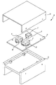
図5及び図6は、ディスクドライブ装置aにおけるプリント基板をその電子部品がマウントされた側を金属製のカバー体で覆ったものを示す。尚、本図においては、ディスクドライブ装置aにおけるディスク回転機構、信号読取機構等の機構は省略する。
【0004】
ディスクドライブ装置aは、上方及び前方に開口した合成樹脂材料製のケース体bと、該ケース体bの下面の下側に配設されるプリント基板cと、該プリント基板cにマウントされた各種の電子部品d、d、・・・と、プリント基板cの下面を覆うカバー体eとを有する。尚、図示は省略したが、ケース体bの上面は別のカバー体により、また、前面はフロントパネルにより覆われる。
【0005】
尚、図5は、ディスクドライブ装置aを上下逆さにして分解した状態を示す斜視図であり、従って、図5において、左斜め下方に向かう方向を前方とし、上方に向かう方向を下側とし、下方に向かう方向を上側とする。
【0006】
プリント基板cにマウントされた電子部品d、d、・・・は、熱をもつことが多く、そのため、放熱を促す必要があり、各電子部品d、d、・・・とカバー体eとの間には、熱伝導性合成樹脂材料から成る放熱用の熱伝導部品fが介在されている(図6参照)。
【0007】
これにより、各電子部品d、d、・・・で生じた熱は、熱伝導部品fを介してカバー体eに伝導され、カバー体eにより外部に放出される。
【0008】
【発明が解決しようとする課題】
ところが、通常、プリント基板cにマウントされた電子部品d、d、・・・は、種々の形状及び大きさをしており、従って、各電子部品d、d、・・・のプリント基板eからの高さはまちまちである(図6参照)。
【0009】
従って、上記したように、従来の電子機器の放熱構造にあっては、各電子部品d、d、・・・とカバー体eとの間の間隔がまちまちであるため、放熱を行うためには、各電子部品d、d、・・・において、厚みの異なった熱伝導部品f、f、・・・をカバー体eとの間に介在させる必要があり、コスト高の要因になっていた。
【0010】
そこで、本発明は、電子部品とカバー体との間に介在させる熱伝導部品の共通化を図り、コストの低減を図ることを課題とする。
【0011】
【課題を解決するための手段】
そこで、本発明は、上記した課題を解決するために、カバー体の電子部品に対応する部位にプリント基板側に突出する突出部を設け、該突出部は対応する電子部品との間の間隔が各突出部間において同じになるように形成され、電子部品と対応する突出部との間に熱伝導性合成樹脂材料から成る放熱用の熱伝導部品を介在させるとともに、カバー体のプリント基板に面した内側面に絶縁シートが貼着され、該絶縁シートのうち突出部に対応する部分に切欠部を形成し、熱伝導部品は、同じ厚さに形成されていると共に、カバー体の突出部と電子部品との間の間隔より厚く形成され、突出部と電子部品との間に挾持されたときに圧潰されるようにし、カバー体の外側面にフィン状の放熱板を形成したものである。
【0012】
従って、本発明にあっては、突出部の下面と電子部品との間の間隔が一定なので、介在させる熱伝導部品の肉厚を一定にすることができ、よって、部品の共通化を図り、コストを低減することができる。また、カバー体のプリント基板に面した内側面に絶縁シートを貼着し、該絶縁シートのうち上記突出部に対応する部分に切欠部を形成したので、熱伝導部品とカバー体とが密接され、絶縁シートを貼着していながら、十分な放熱効果を得ることができる。そして、熱伝導部品がカバー体の突出部と電子部品との間の間隔より厚く形成され、突出部と電子部品との間に挾持されたときに圧潰されるようにしたので、熱伝導部品が突出部と電子部品とに圧接されることによって、熱伝導効率がさらに良くなり、より大きな放熱効果を得ることができる。そして、さらに、カバー体の外側面にフィン状の放熱板を形成しているので、カバー体の冷却をさらに効率良く行うことができる。
【0013】
【発明の実施の形態】
図1は、本発明に係る電子機器及び電子機器の放熱構造の基本構成を概念的に示すものである。
【0014】
電子機器1は、各種電子部品2、2、・・・がマウントされたプリント基板3と、該プリント基板3の電子部品2、2、・・・がマウントされた側を覆う金属製のカバー体4とを備える。
【0015】
電子機器1としては、例えば、ディスクドライブ装置、テーププレーヤー、ディスクプレーヤー、テレビ、ラジオなど各種の電子機器が考えられる。
【0016】
電子機器1は、一般に、各種機構、装置(図示は省略する。)などが、各種電子部品2、2、・・・がマウントされたプリント基板3と共に、ケース体、筐体などに収納され、これらケース体、筐体の一側面にプリント基板3が設けられており、更に該プリント基板3を覆うように金属製のカバー体4が設けられている。本発明は、これらのプリント基板3にマウントされる電子部品2、2、・・・の放熱に関する。
【0017】
プリント基板3とカバー体4との間には、電子部品2、2、・・・がカバー体4に接触しないように適宜な間隙が設けられている。尚、プリント基板3の大きさは、カバー体4とほゞ同じでも又は小さくても良い。
【0018】
電子部品2、2、・・・としては、例えば、IC、LSIなどのように外装がパッケージされた電子部品のほか、放熱を必要とするコイルなどの電子部品も含まれる。
【0019】
カバー体4の上記電子部品2、2、・・・に対応する部位には、プリント基板3側に突出する突出部5、5、・・・が設けられ、各突出部5、5、・・・は、これと対応する電子部品2、2、・・・との間の間隔が各突出部5、5、・・・間において同じになるように形成されている。即ち、各突出部5は、そのカバー体4の上面からの突出量が、予め、対応する電子部品2、2、・・・の大きさ(プリント基板3からの高さ)に応じて、設計される。
【0020】
突出部5により囲まれる部分の空間の形状は、直方体でも角錐台でも良く、その底面が各電子部品2、2、・・・の上面とほゞ平行になるように形成され、また、突出部5の底面の大きさは、対応する電子部品2の上面とほゞ同じに形成されている。
【0021】
そして、突出部5と対応する電子部品2との間に、熱伝導性合成樹脂材料から成る放熱用の熱伝導部品6、6、・・・が介在されている。各熱伝導部品6、6、・・・は、各電子部品2、2、・・・と対応する突出部5、5、・・・との間の間隔が、上述のように、同じに形成されているため、同じ厚さになっている。
【0022】
また、各熱伝導部品6の厚さは、突出部5と対応する電子部品2との間の間隔よりやや厚く形成されており、熱伝導部品6は突出部5と電子部品2との間に挾持されたときに、やや圧潰される。これは、熱伝導部品6と突出部5又は電子部品2とを圧接していた方が、熱伝導効率が良く、放熱効果を得られるからである。
【0023】
尚、突出部5の底面及び熱伝導部品6の接触面の大きさは、対応する電子部品2の上面の大きさより、大きいことが放熱効果の面から好ましいが、放熱を然程必要としない電子部品2については、その電子部品2の上面よりも小さくても良い。
【0024】
熱伝導部品6の材質としては、例えば、天然ゴム、合成ゴムなどのように絶縁性を備え、熱伝導効率の高い材質が選ばれる。
【0025】
【実施例】
以下に、本発明の詳細を添付図面に示した実施例に従って説明する。
【0026】
尚、図2乃至図4に示した実施例は、本発明をディスクドライブ装置のケース体の下面に配設されるプリント基板にマウントされた電子部品の放熱構造7に適用したものである。
【0027】
尚、図2は、ディスクドライブ装置を上下逆さにして分解した状態を示す斜視図であり、従って、図2において、左斜め下方に向かう方向を前方とし、上方に向かう方向を下側とし、下方に向かう方向を上側とする。
【0028】
ディスクドライブ装置8は、合成樹脂材料から成り上面及び前面が開口した箱状のケース体9内に光学ヘッド、スピンドルモータ等の電子部品(図示は省略する。)が収納されている。ケース体9が、合成樹脂材料にて形成されているのは、箱体としてできるだけ面と面との接合部を少なくして、防塵を図るためである。尚、図示は省略したが、ケース体9は、その上面がカバー体により覆われ、また、前面がフロントパネルにより覆われており、これらカバー体及びフロントパネルとケース体9とは防塵対策が図られている。
【0029】
ケース体9の下面には、その全面に扁平な凹部10が形成され、該凹部10には、光学ヘッド、スピンドルモータ等の制御回路、電源回路等が形成されたプリント基板11が配設されている。尚、プリント基板11のこれら制御回路及び電源回路と上記光学ヘッド、スピンドルモータ等との電気的接続を図るため、図示は省略したが、フレキシブルプリント基板がケース体9の底面を貫通するように設けられている。
【0030】
このようにプリント基板11を収納するための凹部10を形成し、光学ヘッド、スピンドルモータなどを収納する空間とを隔離しているのは、光学ヘッドに対する防塵対策を図るためである。
【0031】
プリント基板11には、上記制御回路、電源回路などを構成する各種の電子部品12、12、・・・がマウントされ、また、このようなプリント基板11の下面を覆うように金属製のカバー体13が設けられている。
【0032】
プリント基板11とカバー体13との間には、電子部品12、12、・・・がカバー体13に接触しないように適宜な間隙が設けられており、また、カバー体13のプリント基板11側には絶縁材料から成る絶縁シート14が貼着されている。
【0033】
カバー体13の上記電子部品12、12、・・・に対応する部位には、プリント基板11側に突出する突出部15、15、・・・が設けられ、各突出部15、15、・・・は、これと対応する電子部品12、12、・・・との間の間隔が各突出部15、15、・・・間において同じになるように形成されている。
【0034】
即ち、各突出部15は、そのカバー体13の上面からの突出量を、予め、対応する電子部品12、12、・・・の大きさ(プリント基板11からの高さ)に応じて、設計されており、従って、高さの高い電子部品12に対応した突出部15はその突出量が小さく、高さの低い電子部品12に対応した突出部15はその突出量が大きく形成されている。
【0035】
また、上記絶縁シート14は、各突出部15、15・・・を避けるように切欠部14a、14a、・・・が形成されている。
【0036】
カバー体13の適所には、数本のスリットが形成されると共に、スリットとスリットとの間の部分が切り起されて、フィン状の放熱板16、16・・・が形成されている。これにより、カバー体13とプリント基板11との間の空間に溜まった熱を外部に効率良く放出すると共に、カバー体13の冷却を効率良く行うことができる。尚、カバー体13とプリント基板11との間の空間に溜まった熱は、放熱用スリット、放熱孔などによっても外部に放出することができる。
【0037】
各電子部品12、12、・・・とカバー体13の対応する突出部15、15・・との間には、熱伝導性合成樹脂材料から成る放熱用の熱伝導部品17、17、・・・が各別に介在されている。
【0038】
各電子部品12、12、・・・とカバー体13の対応する突出部15、15・・との間の間隔が同一なので、各熱伝導部品17、17、・・・は、同一の厚さに形成されていると共に、各熱伝導部品17の厚さは、突出部15と対応する電子部品12との間の間隔よりやや厚くなるように形成され、熱伝導部品17は突出部15と電子部品12との間に挾持されたときに、やや圧潰されるようになっている。これにより、熱伝導部品17と突出部15又は電子部品12とが圧接され、熱伝導効率が良く、放熱効果を適確に得ることができる。
【0039】
しかして、各電子部品12、12、・・・で生じた熱は、熱伝導部品17、17、・・・を介してカバー体13に伝達され、カバー体13により外部に放出される。
【0040】
また、カバー体13には、その内側面に絶縁シート14が貼着されているため、カバー体13とプリント基板11との間に、異物、例えば、修理時におけるビスなどが侵入しても、プリント基板11に形成された回路とカバー体13とが短絡することはない。
【0041】
【発明の効果】
以上に記載したところから明らかなように、本発明によれば、カバー体の電子部品に対応する部位にプリント基板側に突出する突出部を設け、該突出部は対応する電子部品との間の間隔が各突出部間において同じになるように形成され、電子部品と対応する突出部との間に熱伝導性合成樹脂材料から成る放熱用の熱伝導部品を介在させたので、突出部の下面と電子部品との間に介在させる熱伝導部品の肉厚を一定にすることができ、よって、部品の共通化を図り、コストを低減することができる。また、カバー体のプリント基板に面した内側面に絶縁シートを貼着し、該絶縁シートのうち上記突出部に対応する部分に切欠部を形成したので、熱伝導部品とカバー体とが密接され、絶縁シートを貼着していながら、十分な放熱効果を得ることができる。そして、熱伝導部品がカバー体の突出部と電子部品との間の間隔より厚く形成され、突出部と電子部品との間に挾持されたときに圧潰されるようにしたので、熱伝導部品が突出部と電子部品とに圧接されることによって、熱伝導効率がさらに良くなり、より大きな放熱効果を得ることができる。そして、さらに、カバー体の外側面にフィン状の放熱板を形成しているので、カバー体の冷却をさらに効率良く行うことができる。
【0043】
尚、前記した実施例において示した各部の具体的な形状乃至構造は、本発明を実施するに当たっての具体化のほんの一例を示したものに過ぎず、これらによって本発明の技術的範囲が限定的に解釈されることがあってはならないものである。
【図面の簡単な説明】
【図1】 本発明に係る電子機器及び電子機器の放熱構造の基本構成を概念的に示す断面図である。
【図2】 図3及び図4と共に本発明の実施の一例を説明するための図であり、本図は分解斜視図である。
【図3】 要部を拡大して示す断面図である。
【図4】 別の要部を拡大して示す断面図である。
【図5】 図6と共に、従来の電子機器の放熱構造を説明するための図であり、本図は分解斜視図である。
【図6】 拡大断面図である。
【符号の説明】
1…電子機器、2…電子部品、3…プリント基板、4…カバー体、5…突出部、6…熱伝導部品、7…電子機器の放熱構造、8…ディスクドライブ装置(電子機器)、11…プリント基板、12…電子部品、13…カバー体、14…絶縁シート、14a…切欠部、15…突出部、16…放熱板、17…熱伝導部品[0001]
BACKGROUND OF THE INVENTION
The present invention relates to a technique for reducing the cost by making a heat conductive component common between an electronic component mounted on a printed circuit board close to a metal cover body and the cover body.
[0002]
[Prior art]
A printed circuit board on which an electronic component is mounted may be covered with a metal cover on the surface of the electronic component.
[0003]
5 and 6 show a printed circuit board in the disk drive device a in which the electronic component mounted side is covered with a metal cover. In this figure, mechanisms such as a disk rotation mechanism and a signal reading mechanism in the disk drive device a are omitted.
[0004]
The disk drive device a includes a case body b made of a synthetic resin material that opens upward and forward, a printed circuit board c disposed below the lower surface of the case body b, and various types mounted on the printed circuit board c. , And a cover body e that covers the lower surface of the printed circuit board c. Although not shown, the upper surface of the case body b is covered with another cover body, and the front surface is covered with a front panel.
[0005]
5 is a perspective view showing a state in which the disk drive device a is disassembled upside down. Accordingly, in FIG. 5, the direction toward the lower left is defined as the front and the direction toward the upper is defined as the lower side. The downward direction is the upper side.
[0006]
The electronic components d, d,... Mounted on the printed circuit board c often have heat. Therefore, it is necessary to promote heat dissipation, and the electronic components d, d,. A heat conducting component f for heat dissipation made of a heat conductive synthetic resin material is interposed therebetween (see FIG. 6).
[0007]
Thereby, the heat generated in each electronic component d, d,... Is conducted to the cover body e through the heat conducting component f, and is released to the outside by the cover body e.
[0008]
[Problems to be solved by the invention]
However, the electronic components d, d,... Mounted on the printed circuit board c usually have various shapes and sizes, and accordingly, from the printed circuit board e of each electronic component d, d,. Varies in height (see FIG. 6).
[0009]
Therefore, as described above, in the heat dissipation structure of the conventional electronic device , the interval between each electronic component d, d,... In each of the electronic components d, d,..., It is necessary to interpose heat conductive components f, f,... Having different thicknesses with the cover body e, resulting in high cost.
[0010]
In view of the above, an object of the present invention is to reduce the cost by sharing a heat conducting component interposed between the electronic component and the cover body.
[0011]
[Means for Solving the Problems]
Therefore, in order to solve the above-described problems, the present invention provides a protruding portion that protrudes toward the printed circuit board at a portion corresponding to the electronic component of the cover body, and the protruding portion is spaced from the corresponding electronic component. A heat conductive component for heat dissipation made of a heat conductive synthetic resin material is interposed between the electronic component and the corresponding protruding portion, and is formed on the printed circuit board of the cover body. An insulating sheet is attached to the inner surface, a notch is formed in a portion corresponding to the protruding portion of the insulating sheet, and the heat conducting parts are formed to the same thickness, and the protruding portion of the cover body It is formed thicker than the gap between the electronic parts and is crushed when sandwiched between the protruding part and the electronic part, and a fin-like heat sink is formed on the outer surface of the cover body.
[0012]
Therefore, in the present invention, since the distance between the lower surface of the protruding portion and the electronic component is constant, the thickness of the heat conduction component to be interposed can be made constant, so that the components can be shared, Cost can be reduced. In addition, an insulating sheet is attached to the inner surface of the cover body facing the printed circuit board , and a cutout portion is formed in a portion corresponding to the protruding portion of the insulating sheet, so that the heat conducting component and the cover body are brought into close contact with each other. A sufficient heat dissipation effect can be obtained while the insulating sheet is adhered. And since the heat conduction component is formed thicker than the interval between the protrusion of the cover body and the electronic component and is crushed when sandwiched between the protrusion and the electronic component, the heat conduction component is By being in pressure contact with the protrusion and the electronic component, the heat conduction efficiency is further improved, and a greater heat dissipation effect can be obtained. Further, since the fin-like heat sink is formed on the outer surface of the cover body, the cover body can be cooled more efficiently.
[0013]
DETAILED DESCRIPTION OF THE INVENTION
FIG. 1 conceptually shows a basic configuration of an electronic device and a heat dissipation structure of the electronic device according to the present invention.
[0014]
The
[0015]
As the
[0016]
In general, the
[0017]
An appropriate gap is provided between the printed circuit board 3 and the cover body 4 so that the
[0018]
The
[0019]
.. Of the cover body 4 corresponding to the
[0020]
The shape of the space surrounded by the protruding portion 5 may be a rectangular parallelepiped or a truncated pyramid, and is formed so that its bottom surface is substantially parallel to the top surface of each
[0021]
And between the protrusion part 5 and the
[0022]
In addition, the thickness of each heat conducting component 6 is formed slightly thicker than the interval between the protruding portion 5 and the corresponding
[0023]
Note that the size of the bottom surface of the protruding portion 5 and the contact surface of the heat conducting component 6 is preferably larger than the size of the upper surface of the corresponding
[0024]
As a material of the heat conductive component 6, for example, a material having insulating properties such as natural rubber and synthetic rubber and having high heat conduction efficiency is selected.
[0025]
【Example】
Details of the present invention will be described below with reference to embodiments shown in the accompanying drawings.
[0026]
In the embodiment shown in FIGS. 2 to 4, the present invention is applied to a heat dissipation structure 7 for an electronic component mounted on a printed circuit board disposed on the lower surface of a case body of a disk drive device.
[0027]
2 is a perspective view showing a state in which the disk drive device is disassembled upside down. Accordingly, in FIG. 2, the direction toward the lower left is defined as the front and the direction toward the upper is defined as the lower side. The direction toward is the upper side.
[0028]
The
[0029]
A flat
[0030]
The reason why the
[0031]
Various
[0032]
An appropriate gap is provided between the printed
[0033]
.. Of the
[0034]
That is, each
[0035]
Further, the insulating
[0036]
Several slits are formed at appropriate positions of the
[0037]
Between the
[0038]
Since the distance between each
[0039]
Therefore, the heat generated in each of the
[0040]
In addition, since the insulating
[0041]
【The invention's effect】
As is apparent from the above description, according to the present invention, a protrusion that protrudes toward the printed circuit board is provided at a portion corresponding to the electronic component of the cover body, and the protrusion is between the corresponding electronic component. The distance between the protrusions is the same, and the heat-dissipating heat conductive component made of a heat conductive synthetic resin material is interposed between the electronic component and the corresponding protrusion. It is possible to make the thickness of the heat conducting component interposed between the electronic component and the electronic component constant, and thus it is possible to share the components and reduce the cost. In addition, an insulating sheet is attached to the inner surface of the cover body facing the printed circuit board , and a cutout portion is formed in a portion corresponding to the protruding portion of the insulating sheet, so that the heat conducting component and the cover body are brought into close contact with each other. A sufficient heat dissipation effect can be obtained while the insulating sheet is adhered. And since the heat conduction component is formed thicker than the interval between the protrusion of the cover body and the electronic component and is crushed when sandwiched between the protrusion and the electronic component, the heat conduction component is By being in pressure contact with the protrusion and the electronic component, the heat conduction efficiency is further improved, and a greater heat dissipation effect can be obtained. Further, since the fin-like heat sink is formed on the outer surface of the cover body, the cover body can be cooled more efficiently.
[0043]
It should be noted that the specific shapes and structures of the respective parts shown in the above-described embodiments are merely examples of implementation in carrying out the present invention, and these limit the technical scope of the present invention. It should not be interpreted.
[Brief description of the drawings]
FIG. 1 is a cross-sectional view conceptually showing the basic structure of an electronic device and a heat dissipation structure for the electronic device according to the present invention.
FIG. 2 is a view for explaining an example of the embodiment of the present invention together with FIGS. 3 and 4, and this figure is an exploded perspective view.
FIG. 3 is an enlarged cross-sectional view showing a main part.
FIG. 4 is an enlarged sectional view showing another main part.
FIG. 5 is a view for explaining a heat dissipation structure of a conventional electronic device together with FIG. 6, and this figure is an exploded perspective view.
FIG. 6 is an enlarged cross-sectional view.
[Explanation of symbols]
DESCRIPTION OF
Claims (2)
該プリント基板の電子部品がマウントされた側を覆う金属製のカバー体とを備え、
カバー体の上記電子部品に対応する部位にプリント基板側に突出する突出部を設け、
該突出部は対応する電子部品との間の間隔が各突出部間において同じになるように形成され、
上記電子部品と対応する突出部との間に熱伝導性合成樹脂材料から成る放熱用の熱伝導部品を介在させるとともに、上記カバー体の上記プリント基板に面した内側面に絶縁シートが貼着され、該絶縁シートのうち上記突出部に対応する部分に切欠部を形成し、
上記熱伝導部品は、同じ厚さに形成されていると共に、カバー体の上記突出部と電子部品との間の間隔より厚く形成され、突出部と電子部品との間に挾持されたときに圧潰されるようにし、
上記カバー体の外側面にフィン状の放熱板を形成した
ことを特徴とする電子機器。A printed circuit board on which electronic components are mounted;
A metal cover body covering the side on which the electronic component of the printed board is mounted,
Providing a projecting portion projecting to the printed circuit board side at a portion corresponding to the electronic component of the cover body
The protrusions are formed such that the distance between the corresponding electronic components is the same between the protrusions,
A heat-dissipating heat-conducting component made of a heat-conducting synthetic resin material is interposed between the electronic component and the corresponding protrusion, and an insulating sheet is attached to the inner surface of the cover body facing the printed circuit board. , Forming a notch in a portion corresponding to the protruding portion of the insulating sheet,
The heat conducting parts are formed to have the same thickness, and are formed to be thicker than the distance between the protruding part of the cover body and the electronic part, and are crushed when sandwiched between the protruding part and the electronic part. To be
An electronic device, wherein a fin-like heat sink is formed on the outer surface of the cover body.
該プリント基板の電子部品がマウントされた側を覆う金属製のカバー体とを備え、
カバー体の上記電子部品に対応する部位にプリント基板側に突出する突出部を設け、
該突出部は対応する電子部品との間の間隔が各突出部間において同じになるように形成され、
上記電子部品と対応する突出部との間に熱伝導性合成樹脂材料から成る放熱用の熱伝導部品を介在させるとともに、上記カバー体の上記プリント基板に面した内側面に絶縁シートが貼着され、該絶縁シートのうち上記突出部に対応する部分に切欠部を形成し、
上記熱伝導部品は、同じ厚さに形成されていると共に、カバー体の上記突出部と電子部品との間の間隔より厚く形成され、突出部と電子部品との間に挾持されたときに圧潰されるようにし、
上記カバー体の外側面にフィン状の放熱板を形成した
ことを特徴とする電子機器の放熱構造。A printed circuit board on which electronic components are mounted;
A metal cover body covering the side on which the electronic component of the printed board is mounted,
Providing a projecting portion projecting to the printed circuit board side at a portion corresponding to the electronic component of the cover body,
The protrusions are formed such that the distance between the corresponding electronic components is the same between the protrusions,
A heat-dissipating heat-conducting component made of a heat-conducting synthetic resin material is interposed between the electronic component and the corresponding protrusion, and an insulating sheet is attached to the inner surface of the cover body facing the printed circuit board. , Forming a notch in a portion corresponding to the protruding portion of the insulating sheet,
The heat conducting parts are formed to have the same thickness, and are formed to be thicker than the distance between the protruding part of the cover body and the electronic part, and are crushed when sandwiched between the protruding part and the electronic part. To be
A heat dissipation structure for an electronic device, wherein a fin-like heat dissipation plate is formed on the outer surface of the cover body.
Priority Applications (1)
| Application Number | Priority Date | Filing Date | Title |
|---|---|---|---|
| JP32780897A JP4326035B2 (en) | 1997-11-28 | 1997-11-28 | Electronic equipment and heat dissipation structure of electronic equipment |
Applications Claiming Priority (1)
| Application Number | Priority Date | Filing Date | Title |
|---|---|---|---|
| JP32780897A JP4326035B2 (en) | 1997-11-28 | 1997-11-28 | Electronic equipment and heat dissipation structure of electronic equipment |
Publications (2)
| Publication Number | Publication Date |
|---|---|
| JPH11163566A JPH11163566A (en) | 1999-06-18 |
| JP4326035B2 true JP4326035B2 (en) | 2009-09-02 |
Family
ID=18203227
Family Applications (1)
| Application Number | Title | Priority Date | Filing Date |
|---|---|---|---|
| JP32780897A Expired - Fee Related JP4326035B2 (en) | 1997-11-28 | 1997-11-28 | Electronic equipment and heat dissipation structure of electronic equipment |
Country Status (1)
| Country | Link |
|---|---|
| JP (1) | JP4326035B2 (en) |
Cited By (2)
| Publication number | Priority date | Publication date | Assignee | Title |
|---|---|---|---|---|
| KR20140131746A (en) * | 2013-05-06 | 2014-11-14 | 삼성전자주식회사 | Controller |
| KR20190000952A (en) * | 2017-06-23 | 2019-01-04 | 네덱 주식회사 | Case and Installing Method of the same |
Families Citing this family (38)
| Publication number | Priority date | Publication date | Assignee | Title |
|---|---|---|---|---|
| JP2002134970A (en) * | 2000-10-26 | 2002-05-10 | Denso Corp | Electronic controller |
| JP2002232172A (en) * | 2001-02-07 | 2002-08-16 | Matsushita Electric Ind Co Ltd | Heat radiating device for electronic component |
| JP2003101270A (en) * | 2001-09-27 | 2003-04-04 | Toshiba Corp | Cooling structure for electronic component, magnetic disk device provided therewith and manufacturing method for cooling structure |
| KR100804565B1 (en) * | 2001-12-27 | 2008-02-20 | 주식회사 만도 | Electric control system for vehicle with radiation and vibroisolating device |
| JP2003289191A (en) | 2002-03-28 | 2003-10-10 | Denso Corp | Electronic control device |
| JP2004030837A (en) * | 2002-06-27 | 2004-01-29 | Toshiba Corp | Storage device and electronic apparatus |
| JP4015497B2 (en) | 2002-07-30 | 2007-11-28 | 日本オプネクスト株式会社 | Optical communication device |
| JP2004140289A (en) * | 2002-10-21 | 2004-05-13 | Funai Electric Co Ltd | Heat radiation structure of electronic component and disk drive device comprising it |
| KR100532461B1 (en) * | 2003-08-21 | 2005-12-01 | 삼성전자주식회사 | Disk drive having heat sinking apparatus |
| JP4352149B2 (en) * | 2004-01-13 | 2009-10-28 | 独立行政法人 日本原子力研究開発機構 | Neutron glass scintillator |
| JP4723299B2 (en) * | 2005-07-11 | 2011-07-13 | マスプロ電工株式会社 | Electronics |
| JP5069876B2 (en) * | 2006-07-13 | 2012-11-07 | 新光電気工業株式会社 | Semiconductor module and heat sink |
| JP4824624B2 (en) * | 2007-05-15 | 2011-11-30 | 株式会社リコー | Heat transfer member, heat transfer mechanism and information processing apparatus |
| JP4508214B2 (en) * | 2007-05-23 | 2010-07-21 | ソニー株式会社 | Display device |
| JP2010108731A (en) * | 2008-10-30 | 2010-05-13 | Kyocera Corp | Illuminating device |
| JP2010108879A (en) * | 2008-10-31 | 2010-05-13 | Toshiba Lighting & Technology Corp | Electric equipment and luminaire |
| JP5434300B2 (en) * | 2009-06-26 | 2014-03-05 | 東芝ライテック株式会社 | Electrical equipment and lighting equipment |
| JP5514309B2 (en) * | 2010-06-14 | 2014-06-04 | シャープ株式会社 | Electronic device, display device, and television receiver |
| JP2013004108A (en) * | 2011-06-10 | 2013-01-07 | Toshiba Corp | Information storage device and electronic equipment |
| KR101229656B1 (en) * | 2011-08-24 | 2013-02-04 | 김근배 | Radiate structure of switching mode power supply using the same |
| JP2013197405A (en) * | 2012-03-21 | 2013-09-30 | Hitachi Automotive Systems Ltd | Electronic control device |
| JP5733260B2 (en) * | 2012-04-09 | 2015-06-10 | 株式会社村田製作所 | Power module |
| JP2014045344A (en) * | 2012-08-27 | 2014-03-13 | Canon Inc | Electronic apparatus |
| JP2014143843A (en) * | 2013-01-24 | 2014-08-07 | Nissan Motor Co Ltd | Contactless power supply device |
| JP6027945B2 (en) * | 2013-06-05 | 2016-11-16 | 株式会社デンソー | Electronic control unit |
| WO2015053141A1 (en) * | 2013-10-07 | 2015-04-16 | 日立オートモティブシステムズ株式会社 | Dc-dc converter device |
| WO2016158759A1 (en) | 2015-03-27 | 2016-10-06 | テイ・エス テック株式会社 | Chair |
| JP6963191B2 (en) * | 2015-03-31 | 2021-11-05 | テイ・エス テック株式会社 | Chair |
| WO2017098899A1 (en) * | 2015-12-11 | 2017-06-15 | 株式会社オートネットワーク技術研究所 | Electrical junction box |
| JP6402942B2 (en) * | 2015-12-11 | 2018-10-10 | 株式会社オートネットワーク技術研究所 | Electrical junction box |
| JP6791238B2 (en) * | 2016-02-22 | 2020-11-25 | コニカミノルタ株式会社 | Portable radiation imaging device |
| KR200483570Y1 (en) * | 2016-06-21 | 2017-05-30 | 주식회사 케이엠더블유 | Switching mode power supply |
| JP6610497B2 (en) | 2016-10-14 | 2019-11-27 | オムロン株式会社 | Electronic device and manufacturing method thereof |
| JP2018098927A (en) * | 2016-12-14 | 2018-06-21 | 株式会社オートネットワーク技術研究所 | Electric connection box |
| JP6766692B2 (en) * | 2017-03-01 | 2020-10-14 | 株式会社デンソー | Electronic device |
| JP2018164324A (en) | 2017-03-24 | 2018-10-18 | 株式会社オートネットワーク技術研究所 | Electric connection box |
| KR102494995B1 (en) | 2017-08-08 | 2023-02-03 | 에이치엘만도 주식회사 | Motor-electric control unit assembly for integrated brake apparatus |
| WO2023199481A1 (en) * | 2022-04-14 | 2023-10-19 | 三菱電機株式会社 | Control apparatus and control panel |
-
1997
- 1997-11-28 JP JP32780897A patent/JP4326035B2/en not_active Expired - Fee Related
Cited By (3)
| Publication number | Priority date | Publication date | Assignee | Title |
|---|---|---|---|---|
| KR20140131746A (en) * | 2013-05-06 | 2014-11-14 | 삼성전자주식회사 | Controller |
| KR102148201B1 (en) * | 2013-05-06 | 2020-08-26 | 삼성전자주식회사 | Controller |
| KR20190000952A (en) * | 2017-06-23 | 2019-01-04 | 네덱 주식회사 | Case and Installing Method of the same |
Also Published As
| Publication number | Publication date |
|---|---|
| JPH11163566A (en) | 1999-06-18 |
Similar Documents
| Publication | Publication Date | Title |
|---|---|---|
| JP4326035B2 (en) | Electronic equipment and heat dissipation structure of electronic equipment | |
| EP0755619B1 (en) | An arrangement for shielding and/or cooling electronic components mounted on a circuit board | |
| EP0827373B1 (en) | Electronic control with heat sink | |
| US6222732B1 (en) | Electrical device, in particular a switching and control unit for motor vehicles | |
| EP1178594B1 (en) | Electronic apparatus provided with an electronic circuit substrate | |
| JPH073674Y2 (en) | Electronic device | |
| JPH0680911B2 (en) | Heat dissipation structure of printed wiring board with electronic components | |
| JP2586389B2 (en) | LSI case shield structure | |
| US7133277B2 (en) | Electronic device | |
| JPH0730280A (en) | Shield case | |
| EP1376590A2 (en) | Storage device comprising circuit board on which heat-generating circuit component is mounted | |
| JPH05259670A (en) | Printed circuit board structure | |
| JP4871676B2 (en) | Electronic circuit equipment | |
| US6580612B2 (en) | Electric circuit | |
| JPH0617353Y2 (en) | Electronic device housing structure | |
| JP2693251B2 (en) | Power cooling module | |
| JPH0555781A (en) | Shield structure for electronic device | |
| JP6905016B2 (en) | Mounting board structure | |
| JP2003234585A (en) | Heat radiating structure of electronic component | |
| JPH10333779A (en) | Board supporting device and portable information equipment housing circuit board | |
| JP3601979B2 (en) | Electronics | |
| JPS58201349A (en) | Heat dissipation of integrated circuit | |
| JP2000068671A (en) | Head dissipating equipment | |
| JP2000244157A (en) | Heat radiator for control unit | |
| JPS6386499A (en) | Electric source |
Legal Events
| Date | Code | Title | Description |
|---|---|---|---|
| A521 | Written amendment |
Free format text: JAPANESE INTERMEDIATE CODE: A523 Effective date: 20040123 |
|
| A621 | Written request for application examination |
Free format text: JAPANESE INTERMEDIATE CODE: A621 Effective date: 20040123 |
|
| A977 | Report on retrieval |
Free format text: JAPANESE INTERMEDIATE CODE: A971007 Effective date: 20060927 |
|
| A131 | Notification of reasons for refusal |
Free format text: JAPANESE INTERMEDIATE CODE: A131 Effective date: 20061010 |
|
| A521 | Written amendment |
Free format text: JAPANESE INTERMEDIATE CODE: A523 Effective date: 20061211 |
|
| A02 | Decision of refusal |
Free format text: JAPANESE INTERMEDIATE CODE: A02 Effective date: 20070206 |
|
| A521 | Written amendment |
Free format text: JAPANESE INTERMEDIATE CODE: A523 Effective date: 20070409 |
|
| A911 | Transfer of reconsideration by examiner before appeal (zenchi) |
Free format text: JAPANESE INTERMEDIATE CODE: A911 Effective date: 20070412 |
|
| A912 | Removal of reconsideration by examiner before appeal (zenchi) |
Free format text: JAPANESE INTERMEDIATE CODE: A912 Effective date: 20070511 |
|
| A521 | Written amendment |
Free format text: JAPANESE INTERMEDIATE CODE: A523 Effective date: 20090302 |
|
| A521 | Written amendment |
Free format text: JAPANESE INTERMEDIATE CODE: A523 Effective date: 20090501 |
|
| A01 | Written decision to grant a patent or to grant a registration (utility model) |
Free format text: JAPANESE INTERMEDIATE CODE: A01 |
|
| A61 | First payment of annual fees (during grant procedure) |
Free format text: JAPANESE INTERMEDIATE CODE: A61 Effective date: 20090609 |
|
| FPAY | Renewal fee payment (event date is renewal date of database) |
Free format text: PAYMENT UNTIL: 20120619 Year of fee payment: 3 |
|
| FPAY | Renewal fee payment (event date is renewal date of database) |
Free format text: PAYMENT UNTIL: 20120619 Year of fee payment: 3 |
|
| FPAY | Renewal fee payment (event date is renewal date of database) |
Free format text: PAYMENT UNTIL: 20120619 Year of fee payment: 3 |
|
| FPAY | Renewal fee payment (event date is renewal date of database) |
Free format text: PAYMENT UNTIL: 20130619 Year of fee payment: 4 |
|
| LAPS | Cancellation because of no payment of annual fees |