JP4323946B2 - Exposure equipment - Google Patents
Exposure equipment Download PDFInfo
- Publication number
- JP4323946B2 JP4323946B2 JP2003422932A JP2003422932A JP4323946B2 JP 4323946 B2 JP4323946 B2 JP 4323946B2 JP 2003422932 A JP2003422932 A JP 2003422932A JP 2003422932 A JP2003422932 A JP 2003422932A JP 4323946 B2 JP4323946 B2 JP 4323946B2
- Authority
- JP
- Japan
- Prior art keywords
- carbon dioxide
- liquid
- exposure apparatus
- exposure
- substrate
- Prior art date
- Legal status (The legal status is an assumption and is not a legal conclusion. Google has not performed a legal analysis and makes no representation as to the accuracy of the status listed.)
- Expired - Fee Related
Links
Images


Classifications
-
- G—PHYSICS
- G03—PHOTOGRAPHY; CINEMATOGRAPHY; ANALOGOUS TECHNIQUES USING WAVES OTHER THAN OPTICAL WAVES; ELECTROGRAPHY; HOLOGRAPHY
- G03F—PHOTOMECHANICAL PRODUCTION OF TEXTURED OR PATTERNED SURFACES, e.g. FOR PRINTING, FOR PROCESSING OF SEMICONDUCTOR DEVICES; MATERIALS THEREFOR; ORIGINALS THEREFOR; APPARATUS SPECIALLY ADAPTED THEREFOR
- G03F7/00—Photomechanical, e.g. photolithographic, production of textured or patterned surfaces, e.g. printing surfaces; Materials therefor, e.g. comprising photoresists; Apparatus specially adapted therefor
- G03F7/70—Microphotolithographic exposure; Apparatus therefor
- G03F7/70216—Mask projection systems
- G03F7/70341—Details of immersion lithography aspects, e.g. exposure media or control of immersion liquid supply
-
- G—PHYSICS
- G03—PHOTOGRAPHY; CINEMATOGRAPHY; ANALOGOUS TECHNIQUES USING WAVES OTHER THAN OPTICAL WAVES; ELECTROGRAPHY; HOLOGRAPHY
- G03F—PHOTOMECHANICAL PRODUCTION OF TEXTURED OR PATTERNED SURFACES, e.g. FOR PRINTING, FOR PROCESSING OF SEMICONDUCTOR DEVICES; MATERIALS THEREFOR; ORIGINALS THEREFOR; APPARATUS SPECIALLY ADAPTED THEREFOR
- G03F7/00—Photomechanical, e.g. photolithographic, production of textured or patterned surfaces, e.g. printing surfaces; Materials therefor, e.g. comprising photoresists; Apparatus specially adapted therefor
- G03F7/20—Exposure; Apparatus therefor
- G03F7/2041—Exposure; Apparatus therefor in the presence of a fluid, e.g. immersion; using fluid cooling means
-
- H—ELECTRICITY
- H01—ELECTRIC ELEMENTS
- H01L—SEMICONDUCTOR DEVICES NOT COVERED BY CLASS H10
- H01L21/00—Processes or apparatus adapted for the manufacture or treatment of semiconductor or solid state devices or of parts thereof
- H01L21/67—Apparatus specially adapted for handling semiconductor or electric solid state devices during manufacture or treatment thereof; Apparatus specially adapted for handling wafers during manufacture or treatment of semiconductor or electric solid state devices or components ; Apparatus not specifically provided for elsewhere
- H01L21/67005—Apparatus not specifically provided for elsewhere
- H01L21/67011—Apparatus for manufacture or treatment
- H01L21/6715—Apparatus for applying a liquid, a resin, an ink or the like
Description
本発明は、液浸法を用いた露光装置及び露光方法に関し、例えばICやLSI等の半導体デバイス、CCD等の撮像デバイス、液晶パネル等の表示デバイス、光導波路等の通信デバイス、磁気ヘッド等のデバイスを製造する際に、感光剤が塗布された基板上にマスク上のパターンを転写して高集積度のデバイスを得るリソグラフィ工程に好適なものである。 The present invention relates to an exposure apparatus and an exposure method using an immersion method, such as a semiconductor device such as an IC or LSI, an imaging device such as a CCD, a display device such as a liquid crystal panel, a communication device such as an optical waveguide, or a magnetic head. When manufacturing a device, it is suitable for a lithography process in which a pattern on a mask is transferred onto a substrate coated with a photosensitive agent to obtain a highly integrated device.
従来より、半導体デバイスや液晶パネル等を製造する際に、マスク上のパターンを感光剤が塗布された基板上に露光転写する投影露光装置が使用されている。デバイスの集積度の向上に伴いパターンの一層の微細化が要求されるため、微細なパターンを解像するための投影露光装置の改良がなされてきた。 Conventionally, when a semiconductor device, a liquid crystal panel, or the like is manufactured, a projection exposure apparatus that exposes and transfers a pattern on a mask onto a substrate coated with a photosensitive agent has been used. As the degree of integration of devices has increased, further miniaturization of patterns has been required, so that projection exposure apparatuses for resolving fine patterns have been improved.
投影露光装置の光学系において、解像できるパターンの大きさを表す解像度Rは、(1)式の如きレーリーの式で表される。
R = k1(λ/NA)・・・(1)
ここで、λは露光波長、NAは投影光学系の像側の開口数、k1は基板の露光後の現像プロセス等によって決まる定数であり、通常0.5程度の値を持つ。
In the optical system of the projection exposure apparatus, the resolution R representing the size of a resolvable pattern is represented by a Rayleigh equation such as equation (1).
R = k1 (λ / NA) (1)
Here, λ is the exposure wavelength, NA is the numerical aperture on the image side of the projection optical system, and k1 is a constant determined by the development process after the exposure of the substrate and usually has a value of about 0.5.
(1)式からわかるように、投影露光装置の光学系の解像力は、露光波長が短いほど、また投影光学系の像側の開口数(NA)が大きいほど高くなる。 As can be seen from equation (1), the resolving power of the optical system of the projection exposure apparatus increases as the exposure wavelength is shorter and the numerical aperture (NA) on the image side of the projection optical system is larger.
このため、露光光源については、波長365nmの水銀ランプi線に続いて、波長248nmのKrFエキシマレーザ、波長193nmのArFエキシマレーザが開発され、更に最近では、波長157nmのF2レーザの開発が行なわれている。しかし、露光光源の短波長化により、投影光学系のレンズに用いる材料に関して透過率、一様性、耐久性等の要求を満たすことが難しくなり、装置の高価格化の要因となっている。 Therefore, as the exposure light source, a KrF excimer laser with a wavelength of 248 nm and an ArF excimer laser with a wavelength of 193 nm have been developed following the mercury lamp i line with a wavelength of 365 nm, and more recently, an F2 laser with a wavelength of 157 nm has been developed. ing. However, the shortening of the wavelength of the exposure light source makes it difficult to satisfy the requirements such as transmittance, uniformity, and durability of the material used for the lens of the projection optical system, which increases the cost of the apparatus.
また投影光学系の開口数に関しては、NAが0.85の投影露光装置が商品化され、NAが0.9を超える投影光学系も検討されている。このような高NAの投影露光装置では、大面積にわたって収差の少ない良好な結像特性を得ることが困難なため、マスクと基板とを同期して走査させながら露光をおこなうスキャン露光方式が採用されている。 As for the numerical aperture of the projection optical system, a projection exposure apparatus having an NA of 0.85 has been commercialized, and a projection optical system having an NA exceeding 0.9 has been studied. In such a high NA projection exposure apparatus, it is difficult to obtain good imaging characteristics with small aberrations over a large area, so a scan exposure method is employed in which exposure is performed while the mask and the substrate are scanned synchronously. ing.
しかし、従来の設計においては、投影光学系と基板との間に屈折率が約1の気体の層が介在することのため、原理的にNAを1以上にすることが不可能であった。 However, in the conventional design, since a gas layer having a refractive index of about 1 is interposed between the projection optical system and the substrate, it is impossible in principle to set NA to 1 or more.
一方、等価的に露光波長を短くして解像力を向上させる手段として液浸法が提案されている。これは投影光学系の最終面と基板との間の、従来では気体で満たされていた空間を、液体で満たしつつ投影露光を行う方法である。液浸法を用いる投影露光装置としては、投影光学系の最終面と共に基板の全体を液槽の中に浸す方式(例えば、特許文献1参照。)や、投影光学系と基板に挟まれた空間だけに液体を流す所謂ローカルフィル方式(例えば、特許文献2参照)が知られている。 On the other hand, an immersion method has been proposed as a means for improving the resolution by shortening the exposure wavelength equivalently. This is a method of performing projection exposure while filling the space between the final surface of the projection optical system and the substrate, which has been conventionally filled with gas, with liquid. As a projection exposure apparatus using a liquid immersion method, a system in which the entire substrate is immersed in a liquid tank together with the final surface of the projection optical system (see, for example, Patent Document 1), or a space between the projection optical system and the substrate. A so-called local fill method (for example, see Patent Document 2) is known in which a liquid is allowed to flow only in the tank.
液浸法の利点は、用いる液体の屈折率をnとすると、等価的な露光波長が光源の波長の1/nになることである。このことは、ウエハに結像する光線の最大入射角が液浸法と従来法で等しいと仮定した場合に、同一波長の光源を用いても、解像度が従来法の1/nに向上することを意味する。例えば、光源の波長が193nmで液体が水の場合、屈折率が約1.44であるので、液浸法を用いることで従来法に比べて解像度を1/1.44にすることができる。 The advantage of the immersion method is that the equivalent exposure wavelength is 1 / n of the wavelength of the light source, where n is the refractive index of the liquid used. This means that the resolution can be improved to 1 / n of the conventional method even if a light source of the same wavelength is used, assuming that the maximum incident angle of the light beam imaged on the wafer is the same between the immersion method and the conventional method. Means. For example, when the wavelength of the light source is 193 nm and the liquid is water, the refractive index is about 1.44. Therefore, by using the immersion method, the resolution can be reduced to 1 / 1.44 as compared with the conventional method.
液浸法に用いる液体としては、水が最も一般的である。水は、波長190nm付近までの紫外光に対して良好な透過率を持つ。また、すでに半導体の製造工程において大量に用いられており、ウエハや感光剤との相性が良いという利点がある。
上記液浸法を用いる投影露光装置においては、液体中の気泡による露光に対する影響を防止することが重要である。投影光学系の最終面と基板の間の露光領域に気泡が進入すると、露光光を散乱する。そのため、転写されるパターンの線幅が許容できる範囲を超えて変動し、極端な場合にはデバイスに絶縁やショートが発生するという問題がある。現在知られている、気泡の露光への影響を防止するために最も効果的な方法は、液体の脱気を行うことである。液体に脱気を施すことで、気泡が発生しにくくなり、且つ発生した気泡が短時間で消滅するので、露光への気泡の影響を防止することができる。 In the projection exposure apparatus using the liquid immersion method, it is important to prevent the influence of the bubbles in the liquid on the exposure. When bubbles enter the exposure area between the final surface of the projection optical system and the substrate, the exposure light is scattered. Therefore, there is a problem that the line width of the transferred pattern fluctuates beyond an allowable range, and in an extreme case, insulation or a short circuit occurs in the device. Currently known, the most effective way to prevent the effects of bubble exposure is to degas the liquid. By degassing the liquid, bubbles are less likely to be generated, and the generated bubbles disappear in a short time, so that the influence of bubbles on exposure can be prevented.
ところが、液浸法で広く用いられる水の場合、脱気を行うと比抵抗が増加するので静電気が発生しやすくなるという問題がある。例えば、半導体の製造工程で用いられる純水(不純物の少ない水)では、脱気後の比抵抗が18MΩ・cmにも達する。また、水と接触する基板表面は感光剤が塗布されているため電気的な絶縁性が高い。そのため、基板をステージで移動させると基板表面に静電気が発生する。この静電気は、基板上のデバイスに不良を発生させてしまう。 However, in the case of water widely used in the immersion method, there is a problem that static electricity tends to be generated because the specific resistance increases when deaeration is performed. For example, in pure water (water with few impurities) used in a semiconductor manufacturing process, the specific resistance after deaeration reaches 18 MΩ · cm. In addition, the surface of the substrate that comes into contact with water has high electrical insulation because a photosensitive agent is applied. Therefore, when the substrate is moved on the stage, static electricity is generated on the substrate surface. This static electricity causes a defect on the device on the substrate.
本発明は、上述の問題点に鑑みてなされたもので、基板上の静電気を抑制することが可能な液浸法を用いる露光装置の提供を例示的な目的とする。 The present invention has been made in view of the above-described problems, and an object of the present invention is to provide an exposure apparatus using a liquid immersion method capable of suppressing static electricity on a substrate.
上記目的を達成するために、本発明の一側面としての露光装置は、マスクのパターンを基板に投影する投影光学系と、前記投影光学系と前記基板との間に液体を供給する液体供給装置とを備え、前記液体供給装置は、前記水を脱気する脱気装置と、前記脱気装置により脱気された前記液体に二酸化炭素を注入する注入装置とを有することを特徴とする。 To achieve the above object, an exposure apparatus according to one aspect of the present invention, the liquid supply device for supplying liquid between a projection optical system for projecting a pattern of a mask onto a substrate, the substrate and the projection optical system with the door, the liquid supply apparatus is characterized by comprising: a deaerator for deaerating the water, and an injection device for injecting carbon dioxide into said liquid that has been deaerated by the deaeration apparatus.
本発明の更なる目的又はその他の特徴は、以下、添付の図面を参照して説明される好ましい実施例等によって明らかにされるであろう。 Further objects and other features of the present invention will be made clear by the preferred embodiments described below with reference to the accompanying drawings.
従来よりも、性能の良い露光装置を提供することができる。 It is possible to provide an exposure apparatus with better performance than before.
以下に、本発明の実施の形態を添付の図面に基づいて詳細に説明する。 Embodiments of the present invention will be described below in detail with reference to the accompanying drawings.
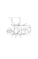
図1は、本発明の投影露光装置の実施例1の要部概略図である。本実施例は本発明を走査型の投影露光装置に適用した場合を示している。
FIG. 1 is a schematic view of the essential portions of
同図において、1は照明系であり、不図示の光源からの光でレチクル(マスク)2を照明している。光源としては、ArFエキシマレーザ(波長193nm)、KrFエキシマレーザ(波長248nm)、F2エキシマレーザ等を用いることができ、照明系1は、公知の光学系等(不図示)から構成されている。3は屈折型またはカタジオプトリック系等の投影光学系であり、照明系1によって照明された第1物体としてのレチクル2の回路パターンを第2物体としてのウエハ5(基板)に投影している。15は測距用レーザ干渉計であり、参照ミラー14を介してレチクルステージ12やウエハステージ13の水平面内の二次元的な位置を計測している。この計測値に基づいてステージ制御装置17がレチクル2やウエハ5の位置決めや同期制御を行う。またウエハステージ13はウエハの上下方向の位置や回転角、傾きを調節する機能を持ち、露光時にウエハ5の表面を投影光学系3の像面と合致させる。
In the figure,
本実施例では、液浸法を用いて等価的な露光波長を短くし、露光における解像度を向上させている。そのため、投影光学系3の最終面の周囲に供給口10と回収口11を配置し、投影光学系3の最終面とウエハ5の間に水を供給して液膜4を形成している。投影光学系3の最終面とウエハ5の間隔は、液膜4が安定に形成できる程度に小さいことが望ましく、例えば、0.5mmとすれば良い。供給口10は供給管8により水を供給する液体供給装置6と結ばれている。回収口11は回収管9により水を回収する液体回収装置7と結ばれている。液体供給装置6は、脱気装置18およびその下流側に設けられた二酸化炭素の注入装置19をその一部として有する。脱気装置18は、例えば公知の膜モジュール(不図示)と真空ポンプ(不図示)により構成される。液浸制御装置16は液体供給装置6および液体回収装置7へ制御信号を送ると同時に、ステージ制御装置17との間でデータの送受信を行う。これにより、液浸制御装置16はウエハの移動方向や速度に応じて液体の供給量と回収量を調節している。
In this embodiment, the equivalent exposure wavelength is shortened by using the immersion method, and the resolution in exposure is improved. Therefore, the
さて本実施例においては、水に脱気を施した後に所定の濃度で二酸化炭素を注入することにより、気泡の露光への影響を防止し、且つ基板上の静電気を抑制する。二酸化炭素は、安価で且つ基板に汚染物質が残さない利点がある。図2により、二酸化炭素の注入装置19の一構成例を説明する。水の流入口20と流出口21の間に膜モジュール22が設けられている。膜モジュール22はバルブ23を介して二酸化炭素の供給源24(例えば炭酸ガスボンベ)に接続されている。バルブ23は二酸化炭素制御装置25により電気的に制御される。
In this embodiment, carbon dioxide is injected at a predetermined concentration after deaeration of water, thereby preventing the influence of bubbles on the exposure and suppressing static electricity on the substrate. Carbon dioxide has the advantage of being inexpensive and leaving no contaminants on the substrate. A configuration example of the carbon
上記の構成によれば、膜モジュール22への二酸化炭素の流量をバルブ23を介して変化させることにより、水中の二酸化炭素濃度を制御することができる。また、二酸化炭素の注入装置の下流側に比抵抗計26を設け、比抵抗計26の出力を二酸化炭素制御装置25へ電気的にフィードバックすることにより二酸化炭素の濃度を所定の範囲に制御すれば尚良い。さらに、膜モジュールを用いる代わりに、ノズルから炭酸ガスを水中に注入しても良い。その場合、炭酸ガス中に存在する微小な粒子をあらかじめフィルタによって除去しておくことが望ましい。
According to the above configuration, the carbon dioxide concentration in the water can be controlled by changing the flow rate of carbon dioxide to the membrane module 22 via the valve 23. Further, if a
以下に、最適な二酸化炭素の濃度について説明する。 The optimum carbon dioxide concentration will be described below.
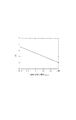
まず、二酸化炭素濃度の下限は、ウエハ上の静電気を抑制する必要性から決定できる。図3に、純水をノズルから噴出してウエハを洗浄した時の、ウエハ上の電位と水の比抵抗の関係を示す(このことについては「純水・超純水の噴霧・接触・流動帯電とその制御」、浅野、電気学会論文誌108巻、1988年、pp.362−366に詳しい。)。同図から、水の比抵抗が10MΩ・cmを超えるとウエハ上に大きな電位が発生し易くなることがわかる。一方、水の比抵抗が5MΩ・cm以下であれば、静電気は問題となりにくい。図4に、純水における二酸化炭素の濃度と比抵抗の関係を示す。二酸化炭素の濃度が高いほど比抵抗が低くなり、比抵抗の10MΩ・cm、5MΩ・cmに対応する二酸化炭素濃度はそれぞれ0.02ppm、0.06ppmである。このことから、ウエハ上の静電気を抑制するために、水中の二酸化炭素濃度は0.02ppm以上とすることが望ましく、0.06ppm以上とすれば尚良い。 First, the lower limit of the carbon dioxide concentration can be determined from the need to suppress static electricity on the wafer. FIG. 3 shows the relationship between the electric potential on the wafer and the specific resistance of water when pure water is ejected from the nozzle and the wafer is cleaned (this is referred to as “spray / contact / flow of pure water / ultra pure water). Charging and its control ", Asano, IEEJ Transactions Volume 108, 1988, pp.362-366. It can be seen from the figure that when the specific resistance of water exceeds 10 MΩ · cm, a large potential is likely to be generated on the wafer. On the other hand, if the specific resistance of water is 5 MΩ · cm or less, static electricity is not a problem. FIG. 4 shows the relationship between the concentration of carbon dioxide in pure water and the specific resistance. The higher the concentration of carbon dioxide, the lower the specific resistance. The carbon dioxide concentrations corresponding to the specific resistances of 10 MΩ · cm and 5 MΩ · cm are 0.02 ppm and 0.06 ppm, respectively. Therefore, in order to suppress static electricity on the wafer, the carbon dioxide concentration in the water is preferably 0.02 ppm or more, and more preferably 0.06 ppm or more.
次に、水中の二酸化炭素濃度の上限は、二気泡の問題を考慮して決定できる。気泡の発生メカニズムには、水中の圧力変動や、二酸化炭素の注入装置における微小な気泡の混入がある。いずれの場合にも、水中の二酸化炭素の濃度が高くなると気泡が発生しやすくなるだけでなく、気泡の寿命(発生した気泡が拡散により消滅するまでの時間)が長くなり、気泡が消えにくくなる。そのため、気泡の露光への影響の危険が増大する。図5に、規格化した気泡の寿命τ/τ0を、規格化した溶存気体の濃度C∞/CSの関数として示す(このことについては、C.E.Brennen,“Cavitation and Bubble Dynamics,”Oxford University Press(1995),Chapter2に詳しい。)。ここで、τ0は、C∞=0.0の場合の気泡の寿命であり、CSは飽和濃度である。濃度C∞/CSが0.2以下の場合、気泡の寿命はC∞=0.0の場合に近いので、比較的に気泡が消えやすい。一方、規格化した濃度C∞/CSが0.5以上になると、気泡の寿命が急激に増大するので、気泡が消えにくくなる。このことから、気泡の露光への影響を防止するためには、水中に溶存する二酸化炭素の濃度を飽和濃度の50%以下とすることが望ましく、20%以下とすれば尚良いことが分かる。水中の二酸化炭素の飽和濃度は一気圧において約1500ppmである。従って、気泡の露光への影響を防止するためには、二酸化炭素の濃度を750ppm以下とすれば良く、300ppm以下とすれば尚良い。これらの値は静電気の抑制のために必要な二酸化炭素の濃度の下限に比べてはるかに大きいので、気泡の影響の防止と静電気の抑制とを両立させることが可能である。 Next, the upper limit of the carbon dioxide concentration in water can be determined in consideration of the problem of two bubbles. Bubble generation mechanisms include pressure fluctuations in water and the inclusion of minute bubbles in a carbon dioxide injection device. In any case, when the concentration of carbon dioxide in water increases, not only bubbles are likely to be generated, but also the lifetime of the bubbles (the time it takes for the generated bubbles to disappear due to diffusion) is prolonged and the bubbles are difficult to disappear. . For this reason, the risk of the influence of the bubble on the exposure increases. 5, the lifetime tau / tau 0 bubbles normalized for shown (this as a function of the concentration C ∞ / C S of dissolved gas were standardized, C.E.Brennen, "Cavitation and Bubble Dynamics , "Detailed to Oxford University Press (1995), Chapter 2.). Here, τ 0 is the lifetime of bubbles when C ∞ = 0.0, and CS is the saturation concentration. When the concentration C∞ / CS is 0.2 or less, the lifetime of the bubbles is close to that when C∞ = 0.0, and the bubbles are relatively easy to disappear. On the other hand, when the standardized concentration C ∞ / CS is 0.5 or more, the lifetime of the bubbles increases rapidly, so that the bubbles are difficult to disappear. From this, it can be seen that the concentration of carbon dioxide dissolved in water is preferably 50% or less of the saturated concentration, and more preferably 20% or less in order to prevent the influence of bubbles on the exposure. The saturated concentration of carbon dioxide in water is about 1500 ppm at 1 atmosphere. Therefore, in order to prevent the influence of the bubble on the exposure, the concentration of carbon dioxide should be 750 ppm or less, and more preferably 300 ppm or less. Since these values are much larger than the lower limit of the concentration of carbon dioxide necessary for suppressing static electricity, it is possible to achieve both prevention of the influence of bubbles and suppression of static electricity.
以上の議論をまとめると、液膜4に供給される水の二酸化炭素の濃度の範囲は0.02ppm以上750ppm以下とすれば良く、0.06ppm以上300ppm以下とすれば尚良い。等価な条件を比抵抗の範囲について表せば、0.02MΩ・cm以上10MΩ・cm以下とすれば良く、0.04MΩ・cm以上5MΩ・cm以下とすれば尚良い。そのようにすることで、気泡の露光への影響を防止して且つ基板上の静電気を抑制することができる。
Summarizing the above discussion, the concentration range of water carbon dioxide supplied to the
さらに、本実施例においては、化学増幅型のレジストに対して好適な酸性の環境を実現できる。化学増幅型のレジストは、KrFレーザやArFレーザを光源とするリソグラフィに最適な高感度のレジストとして広く用いられている。一方、化学増幅型のレジストでは、水中に存在するアンモニア等のアルカリ性の汚染物質がレジスト表面から進入すると化学反応が抑制されてT−topなどのパターン上の問題が生じる。本実施例では、水に二酸化炭素を溶解させることでPH値を下げ、アルカリ性の汚染物質の影響を抑制することができる。図6に、水のPH値と二酸化炭素濃度の関係を示す。 Further, in this embodiment, an acidic environment suitable for a chemically amplified resist can be realized. Chemically amplified resists are widely used as highly sensitive resists suitable for lithography using a KrF laser or ArF laser as a light source. On the other hand, in the chemically amplified resist, when alkaline contaminants such as ammonia existing in water enter from the resist surface, the chemical reaction is suppressed and a pattern problem such as T-top occurs. In the present embodiment, the pH value can be lowered by dissolving carbon dioxide in water, and the influence of alkaline contaminants can be suppressed. FIG. 6 shows the relationship between the pH value of water and the carbon dioxide concentration.
尚、通常、半導体の製造工場においては純水装置が備えられえており、且つその純水装置の多くが脱気の機能を有する。露光装置の外部の純水装置から脱気を施した水を投影露光装置に供給する場合、投影露光装置内の脱気装置18を省略することができる。脱気装置を省略することでコストを低減できる利点がある。以上の考え方に基づく本実施例の露光装置の変形例を図7に示す。この変形例の露光装置は液体供給装置6が脱気装置を有しないことが図1の露光装置と異なっている。本変形例の露光装置における二酸化炭素の注入装置の構成や、最適な水の二酸化炭素の濃度および比抵抗も、上述した図1の露光装置におけるそれらと全く同じである。
Normally, a pure water device is provided in a semiconductor manufacturing factory, and many of the pure water devices have a degassing function. When supplying deaerated water from a pure water apparatus outside the exposure apparatus to the projection exposure apparatus, the
以上、本実施例の液浸法を用いる露光装置によれば、気泡の露光への影響を防止し、且つ基板上の静電気を抑制できる。 As described above, according to the exposure apparatus using the liquid immersion method of the present embodiment, the influence of bubbles on the exposure can be prevented and the static electricity on the substrate can be suppressed.
次に、実施例1に記載の露光装置を利用したデバイスの製造方法の実施例を説明する。
Next, an embodiment of a device manufacturing method using the exposure apparatus described in
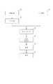
図8はデバイス(ICやLSI等の半導体チップ、液晶パネルやCCD)の製造フローを示す。ステップ1(回路設計)ではデバイスの回路設計を行う。ステップ2(マスク製作)では設計した回路パターンを形成したマスク(レチクル)を製作する。一方、ステップ3(ウエハ製造)ではシリコン等の材料を用いて基板としてウエハを製造する。ステップ4(ウエハプロセス)は前工程と呼ばれ、上記用意したマスクとウエハとを用いて、リソグラフィ技術によってウエハに実際の回路を形成する。次のステップ5(組み立て)は後工程と呼ばれ、ステップ4よって作成されたウエハを用いてチップ化する工程であり、アッセンブリ工程(ダイシング、ボンディング)、パッケージング工程(チップ封入)等の工程を含む。ステップ6(検査)ではステップ5で作成されたデバイスの動作確認テスト、耐久性テスト等の検査を行う。こうした工程を経てデバイスが完成し、これが出荷(ステップ7)される。
FIG. 8 shows a manufacturing flow of devices (semiconductor chips such as IC and LSI, liquid crystal panels and CCDs). In step 1 (circuit design), the device circuit is designed. In step 2 (mask production), a mask (reticle) on which the designed circuit pattern is formed is produced. On the other hand, in step 3 (wafer manufacture), a wafer is manufactured as a substrate using a material such as silicon. Step 4 (wafer process) is called a pre-process, and an actual circuit is formed on the wafer by lithography using the prepared mask and wafer. The next step 5 (assembly) is called a post-process, and is a process for forming a chip using the wafer created in
図9は上記ウエハプロセスの詳細なフローを示す。ステップ11(酸化)ではウエハの表面を酸化させる。ステップ12ではウエハの表面に絶縁膜を形成する。ステップ13(電極形成)ではウエハ上に電極を蒸着によって形成する。ステップ14(イオン打ち込み)ではウエハにイオンを打ち込む。ステップ15(レジスト処理)ではウエハにレジスト(感材)を塗布する。ステップ16(露光)では実施例1に記載の露光装置によってマスクの回路パタ−ンの像でウエハを露光する。ステップ17(現像)では露光したウエハを現像する。ステップ18(エッチング)では現像したレジスト以外の部分を削り取る。ステップ19(レジスト剥離)ではエッチングが済んで不要となったレジストを取り除く。これらステップを繰り返し行うことによりウエハ上に回路パタ−ンが形成される。
FIG. 9 shows a detailed flow of the wafer process. In step 11 (oxidation), the wafer surface is oxidized. In
本実施例の製造方法を用いれば、従来は難しかった高集積度のデバイスを製造することが可能になる。 By using the manufacturing method of this embodiment, it becomes possible to manufacture a highly integrated device, which has been difficult in the past.
以上、本発明の好ましい実施例について説明したが、本発明はこれらの実施例に限定されないことはいうまでもなく、その要旨の範囲内で種々の変形及び変更が可能である。 The preferred embodiments of the present invention have been described above, but the present invention is not limited to these embodiments, and various modifications and changes can be made within the scope of the gist.
1 照明系
2 レチクル(マスク)
3 投影光学系
4 液膜
4a 投影領域
5 ウエハ(基板)
6 液体供給装置
7 液体回収装置
8 供給管
9 回収管
10 供給口
11 回収口
12 レチクルステージ
13 ウエハステージ
14 ミラー
15 測距用レーザ干渉計
16 液浸制御装置
17 ステージ制御装置
18 脱気装置
19 二酸化炭素の注入装置
20 流入口
21 流出口
22 膜モジュール
23 バルブ
24 二酸化炭素の供給源
25 二酸化炭素制御装置
1 Illumination system 2 Reticle (mask)
3 Projection
6
Claims (8)
前記投影光学系と前記基板との間に液体を供給する液体供給装置と、を備え、
前記液体供給装置は、
前記液体を脱気する脱気装置と、
前記脱気装置により脱気された前記液体に二酸化炭素を注入する注入装置と、を有する
ことを特徴とする露光装置。 A projection optical system that projects a mask pattern onto the substrate;
A liquid supply device for supplying a liquid between the projection optical system and the substrate,
The liquid supply device includes:
A degassing device for degassing the liquid;
Exposure apparatus characterized by having, an injection device for injecting carbon dioxide into the liquid which has been deaerated by the deaeration apparatus.
ことを特徴とする請求項1に記載の露光装置。 The exposure apparatus according to claim 1 , wherein the injection apparatus injects carbon dioxide through a membrane module.
ことを特徴とする請求項1または2に記載の露光装置。 It said injection apparatus, an exposure apparatus according to claim 1 or 2 concentration of carbon dioxide of the liquid is characterized in that injection of carbon dioxide to be equal to or less than 750ppm or 0.02 ppm.
ことを特徴とする請求項3に記載の露光装置。 The exposure apparatus according to claim 3, wherein the injection apparatus injects carbon dioxide so that a concentration of carbon dioxide in the liquid is 0.06 ppm or more and 300 ppm or less.
前記注入装置は、前記比抵抗計の計測結果に基づいて二酸化炭素を注入する
ことを特徴とする請求項1または2に記載の露光装置。 The liquid supply apparatus has a specific resistance meter for measuring a specific resistance value of the liquid,
Said injection apparatus, an exposure apparatus according to claim 1 or 2, characterized in that injecting the carbon dioxide based on the measurement result of the resistivity meter.
ことを特徴とする請求項1,2または5に記載の露光装置。 The exposure apparatus according to claim 1 , wherein the injection apparatus injects carbon dioxide so that a specific resistance value of the liquid is 0.02 MΩ · cm or more and 10 MΩ · cm or less.
ことを特徴とする請求項6に記載の露光装置。 The exposure apparatus according to claim 6, wherein the injection apparatus injects carbon dioxide so that a specific resistance value of the liquid is 0.04 MΩ · cm or more and 5 MΩ · cm or less.
ことを特徴とするデバイス製造方法。 A device manufacturing method characterized in that it comprises a step of exposing a substrate using an exposure apparatus according to any one of claims 1 to 7, and a step of developing the substrate with the exposure.
Priority Applications (6)
| Application Number | Priority Date | Filing Date | Title |
|---|---|---|---|
| JP2003422932A JP4323946B2 (en) | 2003-12-19 | 2003-12-19 | Exposure equipment |
| PCT/JP2004/018958 WO2005062351A1 (en) | 2003-12-19 | 2004-12-13 | Exposure apparatus and device manufacturing method |
| US10/538,467 US7292309B2 (en) | 2003-12-19 | 2004-12-13 | Exposure apparatus and device manufacturing method |
| KR1020067011585A KR100801354B1 (en) | 2003-12-19 | 2004-12-13 | Exposure apparatus and device manufacturing method |
| EP04807315A EP1697974A4 (en) | 2003-12-19 | 2004-12-13 | Exposure apparatus and device manufacturing method |
| TW093139536A TWI285796B (en) | 2003-12-19 | 2004-12-17 | Exposure apparatus and device manufacturing method |
Applications Claiming Priority (1)
| Application Number | Priority Date | Filing Date | Title |
|---|---|---|---|
| JP2003422932A JP4323946B2 (en) | 2003-12-19 | 2003-12-19 | Exposure equipment |
Publications (3)
| Publication Number | Publication Date |
|---|---|
| JP2005183693A JP2005183693A (en) | 2005-07-07 |
| JP2005183693A5 JP2005183693A5 (en) | 2007-02-08 |
| JP4323946B2 true JP4323946B2 (en) | 2009-09-02 |
Family
ID=34708744
Family Applications (1)
| Application Number | Title | Priority Date | Filing Date |
|---|---|---|---|
| JP2003422932A Expired - Fee Related JP4323946B2 (en) | 2003-12-19 | 2003-12-19 | Exposure equipment |
Country Status (6)
| Country | Link |
|---|---|
| US (1) | US7292309B2 (en) |
| EP (1) | EP1697974A4 (en) |
| JP (1) | JP4323946B2 (en) |
| KR (1) | KR100801354B1 (en) |
| TW (1) | TWI285796B (en) |
| WO (1) | WO2005062351A1 (en) |
Families Citing this family (51)
| Publication number | Priority date | Publication date | Assignee | Title |
|---|---|---|---|---|
| US7369968B2 (en) | 2000-06-16 | 2008-05-06 | Verisae, Inc. | Enterprise energy management system |
| US7512523B2 (en) | 2000-06-16 | 2009-03-31 | Verisae, Inc. | Refrigerant loss tracking and repair |
| US7474218B2 (en) | 2000-06-16 | 2009-01-06 | Verisae, Inc. | Method and system of asset identification and tracking for enterprise asset management |
| WO2001097146A1 (en) | 2000-06-16 | 2001-12-20 | Verisae | Enterprise asset management system and method |
| US7440871B2 (en) | 2002-12-09 | 2008-10-21 | Verisae, Inc. | Method and system for tracking and reporting emissions |
| US7877235B2 (en) | 2003-01-31 | 2011-01-25 | Verisae, Inc. | Method and system for tracking and managing various operating parameters of enterprise assets |
| JP4837556B2 (en) * | 2003-04-11 | 2011-12-14 | 株式会社ニコン | Optical element cleaning method in immersion lithography |
| KR101697896B1 (en) | 2003-04-11 | 2017-01-18 | 가부시키가이샤 니콘 | Apparatus and method for maintaining immersion fluid in the gap under the projection lens during wafer exchange in an immersion lithography machine |
| TW201806001A (en) * | 2003-05-23 | 2018-02-16 | 尼康股份有限公司 | Exposure device and device manufacturing method |
| EP3104396B1 (en) | 2003-06-13 | 2018-03-21 | Nikon Corporation | Exposure method, substrate stage, exposure apparatus, and device manufacturing method |
| TWI540612B (en) | 2003-06-19 | 2016-07-01 | 尼康股份有限公司 | An exposure apparatus, an exposure method, and an element manufacturing method |
| US6867844B2 (en) | 2003-06-19 | 2005-03-15 | Asml Holding N.V. | Immersion photolithography system and method using microchannel nozzles |
| US6809794B1 (en) | 2003-06-27 | 2004-10-26 | Asml Holding N.V. | Immersion photolithography system and method using inverted wafer-projection optics interface |
| EP1491956B1 (en) | 2003-06-27 | 2006-09-06 | ASML Netherlands B.V. | Lithographic apparatus and device manufacturing method |
| EP1531362A3 (en) * | 2003-11-13 | 2007-07-25 | Matsushita Electric Industrial Co., Ltd. | Semiconductor manufacturing apparatus and pattern formation method |
| JP4295712B2 (en) | 2003-11-14 | 2009-07-15 | エーエスエムエル ネザーランズ ビー.ブイ. | Lithographic apparatus and apparatus manufacturing method |
| CN102163004B (en) | 2003-12-03 | 2014-04-09 | 株式会社尼康 | Exposure apparatus, exposure method and device producing method |
| KR101681852B1 (en) | 2003-12-15 | 2016-12-01 | 가부시키가이샤 니콘 | Stage system, exposure apparatus and exposure method |
| WO2005071717A1 (en) | 2004-01-26 | 2005-08-04 | Nikon Corporation | Exposure apparatus and device producing method |
| US7589822B2 (en) | 2004-02-02 | 2009-09-15 | Nikon Corporation | Stage drive method and stage unit, exposure apparatus, and device manufacturing method |
| WO2005122218A1 (en) * | 2004-06-09 | 2005-12-22 | Nikon Corporation | Exposure system and device production method |
| JP4752473B2 (en) | 2004-12-09 | 2011-08-17 | 株式会社ニコン | Exposure apparatus, exposure method, and device manufacturing method |
| JP2006222165A (en) * | 2005-02-08 | 2006-08-24 | Canon Inc | Exposure device |
| KR100938271B1 (en) | 2005-02-10 | 2010-01-22 | 에이에스엠엘 네델란즈 비.브이. | Immersion liquid, exposure apparatus, and exposure process |
| USRE43576E1 (en) | 2005-04-08 | 2012-08-14 | Asml Netherlands B.V. | Dual stage lithographic apparatus and device manufacturing method |
| US20060232753A1 (en) | 2005-04-19 | 2006-10-19 | Asml Holding N.V. | Liquid immersion lithography system with tilted liquid flow |
| KR101344142B1 (en) * | 2005-04-25 | 2013-12-23 | 가부시키가이샤 니콘 | Exposure method, exposure apparatus and device manufacturing method |
| JP2006319064A (en) | 2005-05-11 | 2006-11-24 | Canon Inc | Measuring device, exposure method and aligner |
| EP1895571A4 (en) * | 2005-06-21 | 2011-04-27 | Nikon Corp | Exposure apparatus, exposure method, maintenance method and device manufacturing method |
| US20070085989A1 (en) * | 2005-06-21 | 2007-04-19 | Nikon Corporation | Exposure apparatus and exposure method, maintenance method, and device manufacturing method |
| WO2007001848A2 (en) * | 2005-06-24 | 2007-01-04 | Sachem, Inc. | High refractive index fluids with low absorption for immersion lithography |
| US7291569B2 (en) * | 2005-06-29 | 2007-11-06 | Infineon Technologies Ag | Fluids for immersion lithography systems |
| US7420188B2 (en) * | 2005-10-14 | 2008-09-02 | Taiwan Semiconductor Manufacturing Company, Ltd. | Exposure method and apparatus for immersion lithography |
| US7773195B2 (en) | 2005-11-29 | 2010-08-10 | Asml Holding N.V. | System and method to increase surface tension and contact angle in immersion lithography |
| WO2007072818A1 (en) * | 2005-12-19 | 2007-06-28 | Nikon Corporation | Liquid producing apparatus, liquid immersion exposure apparatus, and method for manufacturing device |
| JP2007180450A (en) * | 2005-12-28 | 2007-07-12 | Canon Inc | Aligner |
| SG143137A1 (en) | 2006-11-13 | 2008-06-27 | Asml Netherlands Bv | Conduit system for a lithographic apparatus, lithographic apparatus, pump, and method for substantially reducing vibrations in a conduit system |
| US7843548B2 (en) * | 2006-11-13 | 2010-11-30 | Asml Netherlands B.V. | Conduit system for a lithographic apparatus, lithographic apparatus, pump, and method for substantially reducing vibrations in a conduit system |
| US8045135B2 (en) | 2006-11-22 | 2011-10-25 | Asml Netherlands B.V. | Lithographic apparatus with a fluid combining unit and related device manufacturing method |
| JP2008311372A (en) * | 2007-06-13 | 2008-12-25 | Nomura Micro Sci Co Ltd | Measurement method and measuring device of dissolved nitrogen in ultrapure water |
| JP5180555B2 (en) * | 2007-10-04 | 2013-04-10 | キヤノン株式会社 | Positioning apparatus, exposure apparatus, and device manufacturing method |
| JP5097166B2 (en) | 2008-05-28 | 2012-12-12 | エーエスエムエル ネザーランズ ビー.ブイ. | Lithographic apparatus and method of operating the apparatus |
| WO2010103822A1 (en) | 2009-03-10 | 2010-09-16 | 株式会社ニコン | Exposure apparatus, exposure method and device manufacturing method |
| TWI399620B (en) * | 2009-05-05 | 2013-06-21 | Nat Synchrotron Radiation Res Ct | Method for fabricating 3d microstructure |
| NL2005655A (en) | 2009-12-09 | 2011-06-14 | Asml Netherlands Bv | A lithographic apparatus and a device manufacturing method. |
| JP2012009596A (en) * | 2010-06-24 | 2012-01-12 | Nikon Corp | Liquid supply apparatus, exposure equipment, liquid supply method, maintenance method, and method of manufacturing device |
| NL2007453A (en) | 2010-10-18 | 2012-04-19 | Asml Netherlands Bv | A fluid handling structure, a lithographic apparatus and a device manufacturing method. |
| NL2009899A (en) | 2011-12-20 | 2013-06-24 | Asml Netherlands Bv | A pump system, a carbon dioxide supply system, an extraction system, a lithographic apparatus and a device manufacturing method. |
| KR20160138280A (en) * | 2014-03-31 | 2016-12-02 | 고쿠리츠켄큐카이하츠호진 상교기쥬츠 소고켄큐쇼 | Method for manufacturing semiconductor and method for cleaning wafer substrate |
| JP6070784B2 (en) * | 2015-07-14 | 2017-02-01 | 株式会社ニコン | Liquid supply apparatus, exposure apparatus, liquid supply method, and device manufacturing method |
| JP6505534B2 (en) * | 2015-07-22 | 2019-04-24 | 株式会社平間理化研究所 | Method and apparatus for managing developer |
Family Cites Families (14)
| Publication number | Priority date | Publication date | Assignee | Title |
|---|---|---|---|---|
| US5175124A (en) * | 1991-03-25 | 1992-12-29 | Motorola, Inc. | Process for fabricating a semiconductor device using re-ionized rinse water |
| US5825043A (en) | 1996-10-07 | 1998-10-20 | Nikon Precision Inc. | Focusing and tilting adjustment system for lithography aligner, manufacturing apparatus or inspection apparatus |
| JP3747566B2 (en) | 1997-04-23 | 2006-02-22 | 株式会社ニコン | Immersion exposure equipment |
| JP3817836B2 (en) * | 1997-06-10 | 2006-09-06 | 株式会社ニコン | EXPOSURE APPARATUS, ITS MANUFACTURING METHOD, EXPOSURE METHOD, AND DEVICE MANUFACTURING METHOD |
| US5900354A (en) * | 1997-07-03 | 1999-05-04 | Batchelder; John Samuel | Method for optical inspection and lithography |
| JPH11176727A (en) | 1997-12-11 | 1999-07-02 | Nikon Corp | Projection aligner |
| AU2747999A (en) * | 1998-03-26 | 1999-10-18 | Nikon Corporation | Projection exposure method and system |
| JP4608876B2 (en) | 2002-12-10 | 2011-01-12 | 株式会社ニコン | Exposure apparatus and device manufacturing method |
| US7029832B2 (en) * | 2003-03-11 | 2006-04-18 | Samsung Electronics Co., Ltd. | Immersion lithography methods using carbon dioxide |
| KR101176817B1 (en) * | 2003-04-07 | 2012-08-24 | 가부시키가이샤 니콘 | Exposure apparatus and method for manufacturing device |
| US7684008B2 (en) * | 2003-06-11 | 2010-03-23 | Asml Netherlands B.V. | Lithographic apparatus and device manufacturing method |
| TWI245163B (en) * | 2003-08-29 | 2005-12-11 | Asml Netherlands Bv | Lithographic apparatus and device manufacturing method |
| KR101319108B1 (en) * | 2003-09-29 | 2013-10-17 | 가부시키가이샤 니콘 | Projection exposure device, projection exposure method, and device manufacturing method |
| JP2005136374A (en) * | 2003-10-06 | 2005-05-26 | Matsushita Electric Ind Co Ltd | Semiconductor manufacturing apparatus and pattern formation method using the same |
-
2003
- 2003-12-19 JP JP2003422932A patent/JP4323946B2/en not_active Expired - Fee Related
-
2004
- 2004-12-13 WO PCT/JP2004/018958 patent/WO2005062351A1/en not_active Application Discontinuation
- 2004-12-13 KR KR1020067011585A patent/KR100801354B1/en not_active IP Right Cessation
- 2004-12-13 US US10/538,467 patent/US7292309B2/en not_active Expired - Fee Related
- 2004-12-13 EP EP04807315A patent/EP1697974A4/en not_active Withdrawn
- 2004-12-17 TW TW093139536A patent/TWI285796B/en not_active IP Right Cessation
Also Published As
| Publication number | Publication date |
|---|---|
| US20060050257A1 (en) | 2006-03-09 |
| TWI285796B (en) | 2007-08-21 |
| WO2005062351A1 (en) | 2005-07-07 |
| TW200532388A (en) | 2005-10-01 |
| KR100801354B1 (en) | 2008-02-05 |
| US7292309B2 (en) | 2007-11-06 |
| JP2005183693A (en) | 2005-07-07 |
| EP1697974A1 (en) | 2006-09-06 |
| EP1697974A4 (en) | 2009-07-29 |
| KR20060101529A (en) | 2006-09-25 |
Similar Documents
| Publication | Publication Date | Title |
|---|---|---|
| JP4323946B2 (en) | Exposure equipment | |
| US7700267B2 (en) | Immersion fluid for immersion lithography, and method of performing immersion lithography | |
| JP5045437B2 (en) | Exposure apparatus, exposure method, and device manufacturing method | |
| JP4343597B2 (en) | Exposure apparatus and device manufacturing method | |
| JP4652392B2 (en) | Lithographic apparatus and device manufacturing method | |
| US20130278908A1 (en) | Exposure apparatus and exposure method, maintenance method, and device manufacturing method | |
| JP4677833B2 (en) | EXPOSURE APPARATUS, METHOD FOR CLEANING ITS MEMBER, EXPOSURE APPARATUS MAINTENANCE METHOD, MAINTENANCE EQUIPMENT AND DEVICE MANUFACTURING METHOD | |
| US20050185155A1 (en) | Exposure apparatus and method | |
| US20060082749A1 (en) | Exposure apparatus, exposure method, and device fabrication method | |
| JP2005150290A (en) | Exposure apparatus and method of manufacturing device | |
| JP2005020013A (en) | System and method for immersion photolithography using inverted wafer-projection optics interface | |
| US20060170889A1 (en) | Exposure Apparatus, Manufacturing Method of Optical Element, and Device Manufacturing Method | |
| JP2011014929A (en) | Exposure device, exposure device member cleaning method, exposure device maintenance method, maintenance device, and device manufacturing method | |
| TW201022858A (en) | Immersion liquid, exposure apparatus, and exposure process | |
| JP2007281308A (en) | Liquid immersion exposure apparatus | |
| US20080304026A1 (en) | Immersion exposure apparatus and device manufacturing method | |
| US7894036B2 (en) | Exposure apparatus | |
| JP4490459B2 (en) | Exposure apparatus and device manufacturing method | |
| JP2006073906A (en) | Aligner, exposure system, and device manufacturing method | |
| JP2007180450A (en) | Aligner | |
| US8488102B2 (en) | Immersion fluid for immersion lithography, and method of performing immersion lithography | |
| US20060046211A1 (en) | Effectively water-free immersion lithography | |
| JP2007035776A (en) | Exposure device, exposure method, and device manufacturing method | |
| JP2007201252A (en) | Exposure apparatus, and device manufacturing method | |
| JP2009071124A (en) | Exposure apparatus and device manufacturing method |
Legal Events
| Date | Code | Title | Description |
|---|---|---|---|
| A521 | Written amendment |
Free format text: JAPANESE INTERMEDIATE CODE: A523 Effective date: 20061218 |
|
| A621 | Written request for application examination |
Free format text: JAPANESE INTERMEDIATE CODE: A621 Effective date: 20061218 |
|
| A131 | Notification of reasons for refusal |
Free format text: JAPANESE INTERMEDIATE CODE: A131 Effective date: 20090310 |
|
| A521 | Written amendment |
Free format text: JAPANESE INTERMEDIATE CODE: A523 Effective date: 20090430 |
|
| TRDD | Decision of grant or rejection written | ||
| A01 | Written decision to grant a patent or to grant a registration (utility model) |
Free format text: JAPANESE INTERMEDIATE CODE: A01 Effective date: 20090526 |
|
| A01 | Written decision to grant a patent or to grant a registration (utility model) |
Free format text: JAPANESE INTERMEDIATE CODE: A01 |
|
| A61 | First payment of annual fees (during grant procedure) |
Free format text: JAPANESE INTERMEDIATE CODE: A61 Effective date: 20090605 |
|
| R150 | Certificate of patent or registration of utility model |
Free format text: JAPANESE INTERMEDIATE CODE: R150 |
|
| FPAY | Renewal fee payment (event date is renewal date of database) |
Free format text: PAYMENT UNTIL: 20120612 Year of fee payment: 3 |
|
| LAPS | Cancellation because of no payment of annual fees |