JP2005136374A - Semiconductor manufacturing apparatus and pattern formation method using the same - Google Patents
Semiconductor manufacturing apparatus and pattern formation method using the same Download PDFInfo
- Publication number
- JP2005136374A JP2005136374A JP2004157011A JP2004157011A JP2005136374A JP 2005136374 A JP2005136374 A JP 2005136374A JP 2004157011 A JP2004157011 A JP 2004157011A JP 2004157011 A JP2004157011 A JP 2004157011A JP 2005136374 A JP2005136374 A JP 2005136374A
- Authority
- JP
- Japan
- Prior art keywords
- liquid
- unit
- exposure
- pattern
- semiconductor manufacturing
- Prior art date
- Legal status (The legal status is an assumption and is not a legal conclusion. Google has not performed a legal analysis and makes no representation as to the accuracy of the status listed.)
- Pending
Links
Images


Classifications
-
- G—PHYSICS
- G03—PHOTOGRAPHY; CINEMATOGRAPHY; ANALOGOUS TECHNIQUES USING WAVES OTHER THAN OPTICAL WAVES; ELECTROGRAPHY; HOLOGRAPHY
- G03F—PHOTOMECHANICAL PRODUCTION OF TEXTURED OR PATTERNED SURFACES, e.g. FOR PRINTING, FOR PROCESSING OF SEMICONDUCTOR DEVICES; MATERIALS THEREFOR; ORIGINALS THEREFOR; APPARATUS SPECIALLY ADAPTED THEREFOR
- G03F7/00—Photomechanical, e.g. photolithographic, production of textured or patterned surfaces, e.g. printing surfaces; Materials therefor, e.g. comprising photoresists; Apparatus specially adapted therefor
- G03F7/70—Microphotolithographic exposure; Apparatus therefor
- G03F7/70216—Mask projection systems
- G03F7/70341—Details of immersion lithography aspects, e.g. exposure media or control of immersion liquid supply
Abstract
Description
本発明は、半導体装置の製造プロセス等において用いられる半導体製造装置及びそれを用いたパターン形成方法に関する。 The present invention relates to a semiconductor manufacturing apparatus used in a semiconductor device manufacturing process and the like and a pattern forming method using the same.
半導体集積回路の大集積化及び半導体素子のダウンサイジングに伴って、リソグラフィ技術の開発の加速が望まれている。現在のところ、露光光としては、水銀ランプ、KrFエキシマレーザ又はArFエキシマレーザ等を用いる光リソグラフィによりパターン形成が行なわれていると共に、より短波長であるF2 レーザの使用も検討されているが、露光装置及びレジスト材料における課題が未だ多く残されているため、より短波長の露光光を用いる光リソグラフィの実用化の時期は未だ先になっている。 Along with the large integration of semiconductor integrated circuits and downsizing of semiconductor elements, acceleration of development of lithography technology is desired. At present, as exposure light, pattern formation is performed by optical lithography using a mercury lamp, a KrF excimer laser, an ArF excimer laser, or the like, and the use of an F 2 laser having a shorter wavelength is also being studied. However, since many problems still remain in the exposure apparatus and the resist material, the time for practical application of photolithography using exposure light having a shorter wavelength is still ahead.
このような状況から、最近従来の露光光を用いてパターンの一層の微細化を進めるべく、液浸リソグラフィ(immersion lithography)法(非特許文献1を参照。)が提案されている。 Under such circumstances, recently, an immersion lithography method (see Non-Patent Document 1) has been proposed in order to further refine a pattern using conventional exposure light.
この液浸リソグラフィ法によれば、露光装置内における投影レンズとウエハ上のレジスト膜との間の領域が屈折率がn(但し、n>1)である液体で満たされるため、露光装置のNA(開口数)の値がn・NAとなるので、レジスト膜の解像性が向上する。
ところで、従来の液浸型の露光装置には、例えば、図7(a)及び図7(b)に示すように、露光部とウェハ表面との間を満たす液浸用の液体の供給方法に2つの方式がある。図7(a)に示すいわゆる水滴法を用いた露光装置においては、液体250は、ステージ100上に載置されたウェハ200と露光部101との間に、少なくとも露光時の1ショット分のウェハ表面を覆うように局所的に供給される。具体的には、液体250は、1ショットの露光直前に液体供給部110からウェハ200の表面上に供給されて露光された後、次のショットへステージ100が移動する前には液体排出部112から排出される。このように、ウェハ200がステージ100と共にスキャン方向にスライドするのに合わせて、液体250の供給及び排出が1ショットごとに繰り返される。
By the way, in the conventional immersion type exposure apparatus, for example, as shown in FIGS. 7A and 7B, an immersion liquid supplying method that fills a space between the exposure unit and the wafer surface is used. There are two methods. In the exposure apparatus using the so-called water droplet method shown in FIG. 7A, the
これに対し、図7(b)に示すいわゆる液溜(プール)法を用いた露光装置においては、ステージ100上に載置されたウェハ200は液体250を溜めたバス120の中に浸漬されるため、ウェハ表面の全面が液体250に覆われた状態で露光が行なわれる。さらに、1ショットの露光後に次のショットにスキャン移動される際には、露光部101が液体250の液面上を滑るように移動する。
On the other hand, in the exposure apparatus using the so-called liquid pool method shown in FIG. 7B, the
しかしながら、前記従来の液浸リソグラフィ法による露光装置は、いずれの方式であっても、ウェハ200と露光部101との間に配された液体250は露光後に捨てられる。特に、図7(a)に示す水滴法による露光装置を用いる場合は、1ショットごとに液体250の供給及び排出を高速で行なうため、大量の液体250を消費する。
However, in any of the conventional exposure apparatuses using the immersion lithography method, the
また、図7(b)に示す液溜法による露光装置を用いた場合でも、一日に何百枚ものウェハ200に対してパターン露光を行なう量産機では、液体250を定期的に交換する必要があり、やはり大量の液体250を消費する。
Further, even when the exposure apparatus using the liquid pool method shown in FIG. 7B is used, in a mass production machine that performs pattern exposure on hundreds of
従って、液体250を大量に消費することにより、露光のコストが増大し、また、該液体250を捨てる際にも廃液処理が必要となるため、ひいては半導体製造の製造コストが上昇するという問題がある。
Therefore, the consumption of the
本発明は、前記従来の問題を解決し、液浸リソグラフィ法によるパターン形成を低コストで行なえるようにすることを目的とする。 An object of the present invention is to solve the above-mentioned conventional problems and to perform pattern formation by an immersion lithography method at a low cost.
前記の目的を達成するため、本発明は、液浸リソグラフィによる半導体製造装置及びそれを用いたパターン形成方法を、レジスト膜と露光部(投影レンズ)との間に配される開口数の値を増大する液浸用の液体を再利用する構成とする。 In order to achieve the above-described object, the present invention provides a semiconductor manufacturing apparatus using immersion lithography and a pattern forming method using the same, with a numerical aperture value disposed between a resist film and an exposure unit (projection lens). The increasing liquid for immersion is reused.
具体的に、本発明に係るパターン形成方法は、基板の上にレジスト膜を形成する工程と、レジスト膜の上に液体を配した状態で、レジスト膜に対して露光光を選択的に照射してパターン露光を行なう工程と、パターン露光が行なわれたレジスト膜に対して現像を行なってレジストパターンを形成する工程とを備え、パターン露光を行なう工程において、液体には再利用された液体を用いることを特徴とする。 Specifically, the pattern forming method according to the present invention includes a step of forming a resist film on a substrate, and selectively irradiating the resist film with exposure light in a state where a liquid is disposed on the resist film. A pattern exposure step, and a step of developing the resist film subjected to the pattern exposure to form a resist pattern, and in the pattern exposure step, a reused liquid is used as the liquid. It is characterized by that.
本発明のパターン形成方法によると、パターン露光を行なう工程において、レジスト膜と露光部との間に配される液体に再利用された液体を用いるため、露光工程におけるコストの増大を抑制することができる。 According to the pattern forming method of the present invention, in the step of performing pattern exposure, since the reused liquid is used as the liquid disposed between the resist film and the exposed portion, the increase in cost in the exposure step can be suppressed. it can.
本発明のパターン形成方法において、液体はパターン露光を行なう工程中に再利用されることが好ましい。 In the pattern forming method of the present invention, the liquid is preferably reused during the pattern exposure process.
また、本発明のパターン形成方法において、液体はパターン露光を行なう工程の後に回収され、次のパターン露光時に再利用されることが好ましい。 In the pattern forming method of the present invention, it is preferable that the liquid is recovered after the pattern exposure step and reused at the next pattern exposure.
本発明のパターン形成方法において、パターン露光を行なう工程は、液体に混入した不純物を除去する工程を含むことが好ましい。このようにすると、一度露光に用いた液体を再利用する場合でも、露光時に半導体製造装置から又はレジスト膜から混入する不純物が除去されるため、再利用される液体は、不純物の除去によって新しい液体とほぼ同等の純度に戻るので、再利用される液体を介して露光を行なっても、レジスト膜のパターン形成を確実に行なうことができる。 In the pattern forming method of the present invention, it is preferable that the pattern exposure step includes a step of removing impurities mixed in the liquid. In this way, even when the liquid once used for exposure is reused, impurities mixed in from the semiconductor manufacturing apparatus or from the resist film at the time of exposure are removed. As a result, the resist film pattern can be reliably formed even if exposure is performed through the reused liquid.
また、本発明のパターン形成方法は、回収された液体に混入した不純物を除去する工程をさらに備えていることが好ましい。 Moreover, it is preferable that the pattern formation method of this invention is further equipped with the process of removing the impurity mixed in the collect | recovered liquid.
また、本発明のパターン形成方法は、パターン露光を行なう工程よりも前又は後に、液体に混入した不純物を除去する工程をさらに備えていることが好ましい。 Moreover, it is preferable that the pattern formation method of this invention is further equipped with the process of removing the impurity mixed in the liquid before or after the process of performing pattern exposure.
この場合に、不純物を除去する工程は、液体をフィルタに通す工程であることが好ましい。さらにフィルタにケミカルフィルタを用いると、例えば液体に該液体と接触するレジスト膜からアルカリ性又は酸性の化学物質が混入した場合であっても、化学物質を確実に除去することができる。 In this case, the step of removing impurities is preferably a step of passing the liquid through a filter. Furthermore, when a chemical filter is used for the filter, for example, even when an alkaline or acidic chemical substance is mixed into the liquid from a resist film that is in contact with the liquid, the chemical substance can be reliably removed.
また、本発明のパターン形成方法は、不純物を除去する工程の後に、液体に含まれる不純物の組成又は量を検査する工程をさらに備えていることが好ましい。 Moreover, it is preferable that the pattern formation method of this invention is further equipped with the process of test | inspecting the composition or quantity of the impurity contained in a liquid after the process of removing an impurity.
また、本発明のパターン形成方法は、パターン露光を行なう工程の前に、液体に含まれる気体を除去する脱気工程をさらに備えていることが好ましい。このようにすると、液体に含まれる気体(泡)が除去されるため、液体に含まれた泡による露光光の散乱を防止することができるので、形状に優れたパターンを形成することができる。 Moreover, it is preferable that the pattern formation method of this invention is further equipped with the deaeration process which removes the gas contained in a liquid before the process of performing pattern exposure. In this way, since the gas (bubbles) contained in the liquid is removed, the exposure light can be prevented from being scattered by the bubbles contained in the liquid, so that a pattern having an excellent shape can be formed.
本発明に係る半導体製造装置は、基板上に形成されたレジスト膜と露光レンズとの間に液体を配して露光を行なうパターン露光部と、パターン露光部に対して液体が流通可能に接続され、液体をパターン露光部に供給する液体供給部と、パターン露光部に対して液体が流通可能に接続され、液体に含まれる不純物を除去する不純物除去部とを備え、不純物除去部は、液体供給部に対して液体が流通可能に接続され、不純物が除去された液体を液体供給部に移送することを特徴とする。 A semiconductor manufacturing apparatus according to the present invention includes a pattern exposure unit that performs exposure by placing a liquid between a resist film formed on a substrate and an exposure lens, and the liquid is connected to the pattern exposure unit so that the liquid can circulate. A liquid supply unit that supplies the liquid to the pattern exposure unit; and an impurity removal unit that is connected to the pattern exposure unit so that the liquid can circulate and remove impurities contained in the liquid. The liquid is connected to the section so as to be able to flow, and the liquid from which impurities are removed is transferred to the liquid supply section.
本発明の半導体製造装置によると、液体に含まれる不純物を除去する不純物除去部は、液体供給部に対して液体が流通可能に接続され、不純物が除去された液体を液体供給部に移送するため、液浸用の液体を再利用することができるので、液浸用の液体を用いる露光工程におけるコストの増大を抑制することができる。その上、再利用される液体は、不純物除去部によって新しい液体とほぼ同等の純度に戻るため、再利用される液体を介して露光を行なっても、レジスト膜のパターン形成を確実に行なうことができる。 According to the semiconductor manufacturing apparatus of the present invention, the impurity removal unit that removes impurities contained in the liquid is connected to the liquid supply unit so that the liquid can circulate, and transfers the liquid from which the impurities have been removed to the liquid supply unit. Since the liquid for immersion can be reused, an increase in cost in the exposure process using the liquid for immersion can be suppressed. In addition, the reused liquid returns to almost the same purity as the new liquid by the impurity removal unit, so that the resist film pattern can be reliably formed even when exposure is performed through the reused liquid. it can.
本発明の半導体製造装置は、不純物除去部と液体供給部との間に設けられ、液体供給部に移送される液体に含まれる不純物の組成又は量を検査する液体検査部をさらに備えていることが好ましい。 The semiconductor manufacturing apparatus of the present invention further includes a liquid inspection unit that is provided between the impurity removal unit and the liquid supply unit and inspects the composition or amount of impurities contained in the liquid transferred to the liquid supply unit. Is preferred.
また、本発明の半導体製造装置は、パターン露光部から不純物除去部に導入される液体の量を制御する第1の制御部をさらに備えていることが好ましい。 The semiconductor manufacturing apparatus of the present invention preferably further includes a first control unit that controls the amount of liquid introduced from the pattern exposure unit to the impurity removal unit.
本発明の半導体製造装置において、液体供給部は、液体に添加剤を添加する添加部と、液体に添加剤を添加する添加部と、新たな液体、不純物が除去された液体又は調整された添加剤を含む液体をパターン露光部に供給する混合部とを有していることが好ましい。 In the semiconductor manufacturing apparatus of the present invention, the liquid supply unit includes an addition unit for adding an additive to a liquid, an addition unit for adding an additive to a liquid, a new liquid, a liquid from which impurities are removed, or a regulated addition It is preferable to have a mixing unit that supplies the liquid containing the agent to the pattern exposure unit.
この場合に、本発明の半導体製造装置は、添加部から混合部に添加される添加剤の量を制御する第2の制御部をさらに備えていることが好ましい。 In this case, it is preferable that the semiconductor manufacturing apparatus of the present invention further includes a second control unit that controls the amount of the additive added from the addition unit to the mixing unit.
また、本発明の半導体製造装置は、液体供給部とパターン露光部との間に設けられ、パターン露光部に供給される液体に含まれる気体を除去する脱気部をさらに備えていることが好ましい。 The semiconductor manufacturing apparatus of the present invention preferably further includes a deaeration unit that is provided between the liquid supply unit and the pattern exposure unit and removes gas contained in the liquid supplied to the pattern exposure unit. .
本発明の半導体製造装置において、不純物除去部は、液体に含まれる不純物を除去するフィルタを有していることが好ましい。 In the semiconductor manufacturing apparatus of the present invention, it is preferable that the impurity removing unit has a filter for removing impurities contained in the liquid.
本発明の半導体製造装置において除去される不純物はパーティクル又は化学物質であることが好ましい。 The impurities removed in the semiconductor manufacturing apparatus of the present invention are preferably particles or chemical substances.
この場合に除去される化学物質は、アミン、酸又は低分子量ポリマーであることが好ましい。 The chemical removed in this case is preferably an amine, an acid or a low molecular weight polymer.
また、本発明の半導体製造装置は、パターン露光部と不純物除去部との間に設けられた第1のモニタを介して液体の量を制御する第3の制御部をさらに備えていることが好ましい。 The semiconductor manufacturing apparatus of the present invention preferably further includes a third control unit that controls the amount of liquid via a first monitor provided between the pattern exposure unit and the impurity removal unit. .
また、本発明の半導体製造装置は、混合部に導入される添加剤の量及び新たな液体の量のうちの少なくとも一方を、混合部に設けられた第2のモニタを介して制御する第4の制御部をさらに備えていることが好ましい。 In addition, the semiconductor manufacturing apparatus of the present invention controls the at least one of the amount of additive introduced into the mixing unit and the amount of new liquid through a second monitor provided in the mixing unit. It is preferable to further include a control unit.
本発明のパターン形成方法及びその半導体製造装置において、液体には水又はパーフルオロポリエーテルを用いることができる。 In the pattern forming method and the semiconductor manufacturing apparatus of the present invention, water or perfluoropolyether can be used as the liquid.
本発明のパターン形成方法及びその半導体製造装置において、露光光には、KrFエキシマレーザ光、Xe2 エキシマレーザ光、ArFエキシマレーザ光、F2 レーザ光、KrArレーザ光又はAr2 レーザ光を用いることができる。 In the pattern forming method and the semiconductor manufacturing apparatus of the present invention, KrF excimer laser light, Xe 2 excimer laser light, ArF excimer laser light, F 2 laser light, KrAr laser light, or Ar 2 laser light is used as exposure light. Can do.
本発明に係る液浸リソグラフィによるパターン形成方法及び半導体製造装置によると、良好な形状を持つ微細パターンを低コストで得ることができる。 According to the pattern forming method by immersion lithography and the semiconductor manufacturing apparatus according to the present invention, a fine pattern having a good shape can be obtained at low cost.
本発明の第1の実施形態について図面を参照しながら説明する。 A first embodiment of the present invention will be described with reference to the drawings.
(半導体製造装置)
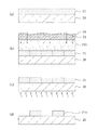
図1(a)及び図1(b)は本発明の第1の実施形態に係る液浸リソグラフィによるパターン形成方法を実現する半導体製造装置であって、(a)は半導体製造装置の要部の断面構成を模式的に示し、(b)は半導体製造装置におけるリサイクル部を模式的に示している。
(Semiconductor manufacturing equipment)
FIG. 1A and FIG. 1B are semiconductor manufacturing apparatuses that realize a pattern forming method by immersion lithography according to the first embodiment of the present invention, and FIG. 1A is a main part of the semiconductor manufacturing apparatus. A cross-sectional configuration is schematically shown, and (b) schematically shows a recycling unit in the semiconductor manufacturing apparatus.
図1(a)に示すように、第1の実施形態に係る半導体製造装置は、チャンバ10内に設けられ、ウェハ20上に塗布されたレジスト膜(図示せず)に設計パターンを露光する露光部30と、露光時にウェハ20の上に、露光光の開口数値を上げる液浸リソグラフィ用の液体23を再利用しながら供給する液体リサイクル部40とから構成されている。
As shown in FIG. 1A, the semiconductor manufacturing apparatus according to the first embodiment is provided in a
露光部30は、ウェハ20を保持するウェハステージ31と、該ウェハステージ31を保持する定盤32と、ウェハ20の上方に設けられウェハステージ31と対向する露光光源を含む照明系33と、該照明系33とウェハステージ31との間に設けられ、レジスト膜に転写される設計パターンを有するマスク(レチクル)22を通って入射される照明系33からの露光光を液体23を介してレジスト膜に投影する投影レンズ34とにより構成される。
The
ここで、投影レンズ34は、露光時にはウェハ20のレジスト膜上に供給された液体23の表面に接するように保持される。
Here, the
液体リサイクル部40は、図1(a)及び図1(b)に示すように、ウェハ20のレジスト膜の上に液体23を供給する液体供給部41と、露光後にレジスト膜上に配された液体23を排出して回収する液体排出部42と、回収された液体23を収納すると共に回収された液体23に含まれる不純物を除去する不純物除去部43とから構成されている。
As shown in FIGS. 1A and 1B, the
ここで、不純物除去部43には、図示はしていないが、液体23をウェハ20上に供給する供給用ポンプと、液体23をウェハ20上から回収する回収用ポンプとが設けられている。
Here, although not shown, the
また、回収された液体23には、不純物として、例えばパーティクルだけでなくレジスト膜等から溶け出した化学物質も含まれており、化学物質をも除去できるように、不純物除去部43には、パーティクルを除去可能なメカニカルフィルタ(パーティクルフィルタ)431と、化学物質を除去可能なケミカルフィルタ432とを設けている。
Further, the recovered
ここで、化学物質の具体例としては、レジスト膜及びその周辺部から溶け出すアミン類、アンモニア又はヘキサメチルジシラザン等のアルカリ性の物質や、トリフルオロメタンスルフォン酸若しくはノナフルオロブタンスルフォン酸等のレジスト膜に含まれる酸発生剤に由来する酸、又は硫酸等の酸性の物質や、レジスト膜からのアウトガス等がある。 Here, specific examples of chemical substances include resist films and alkaline substances such as amines, ammonia or hexamethyldisilazane that dissolve from the periphery thereof, and resist films such as trifluoromethane sulfonic acid or nonafluorobutane sulfonic acid. There are acids derived from the acid generator contained in the acid generator, acidic substances such as sulfuric acid, outgas from the resist film, and the like.
このように、第1の実施形態によると、液浸リソグラフィに用いる液体23を回収し、さらに、回収した液体23に含まれるパーティクルのみならず、露光時にレジスト膜から溶け込んだアウトガス等の化学物質をも除去する液体リサイクル部40を備えているため、例えばパーフルオロポリエーテルからなる液体23の純度を維持することができるので、液体23を確実に再利用でき、その結果、液浸リソグラフィによる露光コストの増大を抑えることができる。 As described above, according to the first embodiment, the liquid 23 used in the immersion lithography is recovered, and not only particles contained in the recovered liquid 23 but also chemical substances such as outgas dissolved from the resist film at the time of exposure. Since the purity of the liquid 23 made of, for example, perfluoropolyether can be maintained, the liquid 23 can be reliably reused. As a result, the exposure cost by immersion lithography can be maintained. Can be suppressed.
なお、ここでは、不純物を除去するフィルタとして、メカニカルフィルタ431とケミカルフィルタ432とを設けたが、いずれか一方でも構わない。しかしながら、液体23の純度を高度に維持するには、両方のフィルタを設けることが好ましい。
Here, the
(半導体製造装置の一変形例)
図2に本発明の第1の実施形態に係る半導体製造装置の一変形例を示す。図2において、図1(a)及び図1(b)に示す構成部材と同一の構成部材には同一の符号を付すことにより説明を省略する。
(One variation of semiconductor manufacturing equipment)
FIG. 2 shows a modification of the semiconductor manufacturing apparatus according to the first embodiment of the present invention. In FIG. 2, the same components as those shown in FIG. 1A and FIG.
図2に示すように、本変形例に係る半導体製造装置は、液浸リソグラフィ用の液体23を再利用しながら供給する液体リサイクル部40を、チャンバ10の外部に設ける構成である。このように液体リサイクル部40をチャンバ10の外部に設けると、チャンバ10内の清浄度をより高く維持することが可能となる。
As shown in FIG. 2, the semiconductor manufacturing apparatus according to the present modification has a configuration in which a
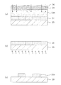
(パターン形成方法)
以下、前記のように構成された半導体製造装置をパターン形成方法について図3(a)〜図3(d)及び図4(a)〜図4(c)を参照しながら説明する。
(Pattern formation method)
Hereinafter, the semiconductor manufacturing apparatus configured as described above will be described with reference to FIGS. 3A to 3D and FIGS. 4A to 4C with respect to a pattern forming method.
まず、以下の組成を有するポジ型の化学増幅型レジスト材料を準備する。 First, a positive chemically amplified resist material having the following composition is prepared.
ポリ(スチレンヘキサフルオロイソプロピルアルコール)(40mol%)−(α-トリフルオロメチル-t-ブチルアクリレート)(60mol%))(ベースポリマー)………………………2g
トリフェニルスルフォニウムトリフレート(酸発生剤)………………………0.08g
プロピレングリコールモノメチルエーテルアセテート(溶媒)……………………20g
次に、図3(a)に示すように、ウェハ20の上に前記の化学増幅型レジスト材料を塗布して、0.20μmの厚さを持つレジスト膜21を形成する。
Poly (styrene hexafluoroisopropyl alcohol) (40mol%)-(α-trifluoromethyl-t-butyl acrylate) (60mol%)) (base polymer) …………………… 2g
Triphenylsulfonium triflate (acid generator) …………………… 0.08g
Propylene glycol monomethyl ether acetate (solvent) ……………… 20g
Next, as shown in FIG. 3A, the chemically amplified resist material is applied on the
次に、図3(b)に示すように、パーフルオロポリエーテルからなる液体23Aをレジスト膜21と投影レンズ34との間に配した状態で、開口数NAが0.60であるF2 レーザよりなる露光光24を図示しないマスクを介してレジスト膜21に照射してパターン露光を行なう。
Next, as shown in FIG. 3B, an F 2 laser having a numerical aperture NA of 0.60 with a liquid 23A made of perfluoropolyether disposed between the resist
次に、図3(c)に示すように、パターン露光が行なわれたレジスト膜21に対して、ホットプレートにより100℃の温度下で60秒間加熱した後、2.38wt%のテトラメチルアンモニウムハイドロキサイド現像液(アルカリ性現像液)により現像を行なうと、図3(d)に示すように、レジスト膜21の未露光部よりなり0.06μmのライン幅を有し且つ良好な形状を持つレジストパターン21aを得られる。
Next, as shown in FIG. 3C, the resist
次に、露光に使用された液体23Aを、例えば図1(b)に示す液体排出部42を介して不純物除去部43に回収し、さらに該不純物除去部43においてパーティクル及びレジスト膜21から溶け出した化学物質を除去する。
Next, the liquid 23A used for the exposure is recovered in the
次に図4(a)に示すように、次のウェハ20の主面上に形成されたレジスト膜21の上に、液体供給部41からリサイクルされた液体23Bを投影レンズ34との間に配し、開口数NAが0.60であるF2 レーザよりなる露光光24を図示しないマスクを介してレジスト膜21に照射してパターン露光を行なう。
Next, as shown in FIG. 4A, the liquid 23B recycled from the
次に、図4(b)に示すように、パターン露光が行なわれたレジスト膜21に対して、ホットプレートにより100℃の温度下で60秒間加熱した後、2.38wt%のテトラメチルアンモニウムハイドロキサイド現像液により現像を行なうと、図4(c)に示すように、レジスト膜21の未露光部よりなり0.06μmのライン幅を有し且つ良好な形状を持つレジストパターン21aを再現性良く得ることができる。
Next, as shown in FIG. 4B, the resist
以上説明したように、第1の実施形態によると、1度目の露光後に回収された液体23Aから不純物を除去して、2度目の露光用の液体23Bとして再利用するため、液浸リソグラフィによる微細パターンを実現しながら、液浸リソグラフィ用の液体の大量消費による露光コストの増大を抑えることができる。 As described above, according to the first embodiment, impurities are removed from the liquid 23A collected after the first exposure and reused as the liquid 23B for the second exposure. While realizing the pattern, it is possible to suppress an increase in exposure cost due to a large consumption of liquid for immersion lithography.
なお、本実施形態において、照明系33に設ける光源の露光光は、F2 レーザ光に限られず、KrFエキシマレーザ光、Xe2 エキシマレーザ光、ArFエキシマレーザ光、KrArレーザ光又はAr2 レーザ光等を適宜用いることができる。
In the present embodiment, the exposure light of the light source provided in the
また、液浸リソグラフィ用の液体23、23A、23bには、パーフルオロポリエーテルに代えて、水を用いることができる。
Further, water can be used for the
(第2の実施形態)
以下、本発明の第2の実施形態について説明する。
(Second Embodiment)
Hereinafter, a second embodiment of the present invention will be described.
ところで、図7(b)に示した液溜法による従来の露光装置の場合においても、液浸用の液体250は前述したように定期的に交換する必要がある。それは、露光時においてウェハ200上に成膜されたレジスト膜は、露光領域以外の部分においても液体250と常に接触しており、液体250とレジスト膜との接触面積が大きく、また接触時間が長いためである。
Incidentally, even in the case of the conventional exposure apparatus based on the liquid pool method shown in FIG. 7B, the
通常、レジストは複数の物質の混合体として構成されており、露光時にはレジストから酸が発生する。従って、液浸用の液体250に、レジストが容易には溶解しにくい特性を持つ液体を用いたとしても、液体250中にレジストから発生する酸や、レジストを構成する化合物が溶出することを完全に防ぐことは難しい。すなわち、液体250を複数のウェハ200の露光に連続して用いると、液体250に不純物が混入して汚染されるという問題が生じる。不純物の混入により液浸用の液体250の純度が低下すると、露光部101からの露光光が、混入した不純物によって散乱されたり、また部分的に吸収されたりする等して、ウェハ200の露光領域に照射される露光量のばらつきが大きくなり、その結果、精度良くパターン露光を行なうことが困難となる。
Usually, a resist is configured as a mixture of a plurality of substances, and an acid is generated from the resist during exposure. Accordingly, even if a liquid having a characteristic that resist is not easily dissolved is used as the
そこで、液浸用の液体250を再利用する際には、液体250中に含まれた不純物及び汚染物質を除去することにより、液体250の当初の純度に戻す必要がある。 Therefore, when the liquid 250 for immersion is reused, it is necessary to return to the original purity of the liquid 250 by removing impurities and contaminants contained in the liquid 250.
次に、本発明の第2の実施形態に係る半導体製造装置について図面を参照しながら説明する。 Next, a semiconductor manufacturing apparatus according to a second embodiment of the present invention will be described with reference to the drawings.
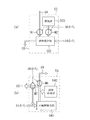
図5は本発明の第2の実施形態に係る液浸リソグラフィを実施可能な半導体製造装置のブロック構成を示している。 FIG. 5 shows a block configuration of a semiconductor manufacturing apparatus capable of performing immersion lithography according to the second embodiment of the present invention.
図5に示すように、第2の実施形態に係る半導体製造装置は、ウェハ上に成膜されたレジスト膜に所定のパターンを露光するパターン露光部51と、レジスト膜と投影レンズとの間に配する液浸用の液体をパターン露光部に供給する液体供給部52と、パターン露光に用いられ排出された液体を回収して液体供給部52に再度供給する液体リサイクル部54とを備えている。
As shown in FIG. 5, the semiconductor manufacturing apparatus according to the second embodiment includes a
液体供給部52とパターン露光部51との間には、液体中に含まれる泡を除去する脱気部(脱泡部)55が設けられ、液体の供給量及び回収量を監視(モニタ)し、さらには液体リサイクル部54において回収された液体の純度を監視して制御する制御部56が設けられている。パターン露光部51には、露光に用いられた液体を排出可能なように、第1の排出口57が設けられている。
A degassing unit (defoaming unit) 55 for removing bubbles contained in the liquid is provided between the
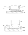
ここで、図6(a)及び図6(b)に液体供給部52及び液体リサイクル部54の構成をそれぞれ示す。
Here, FIGS. 6A and 6B show the configurations of the
液体供給部52は、図6(a)に示すように、液体混合部521と、液体に該液体の光学的且つ電気的な特性を調整可能な添加剤を添加する添加部522とから構成されている。液体混合部521には、供給口58からの新たな液浸用の液体と、液体リサイクル部54からの一旦露光に使用された液体とが導入されると共に、添加部522から液体の屈折率や液体の電気抵抗率を調整可能な化合物、例えば硫酸セシウム(CsSO4 )又はエチルアルコール(C2H5OH)等が必要に応じて添加される。
As shown in FIG. 6A, the
液体リサイクル部54は、図6(b)に示すように、パターン露光部51から回収された液体に混入した不純物を除去する不純物除去部541と、不純物が除去された液体の純度を検査する液体検査部542とから構成されている。ここで、不純物除去部541には、液体検査部542による検査の結果、再利用が不適であると判定された液体を排出する第2の排出口59が設けられている。
As shown in FIG. 6B, the
以下、上記のように構成された半導体製造装置の動作について説明する。 Hereinafter, an operation of the semiconductor manufacturing apparatus configured as described above will be described.
(1)供給口58から液体供給部52に至る動作
まず、図6(a)に示すように、純度が高い液浸用の液体、例えば水(純水)又はパーフルオロポリエーテルを供給口58から液体供給部52の液体混合部521に導入して一時的に溜めておく。液体に添加剤を注入する必要がない場合は、供給口58から純度の高い液体が液体供給部52を通ってパターン露光部51に供給される。
(1) Operation from
液体に添加剤を加える場合は、液体混合部521に貯留された液体に添加部522から適量の添加剤が注入される。
When an additive is added to the liquid, an appropriate amount of additive is injected from the
ここで、図5に示す制御部56は、供給口58に設けられた第1モニタM1を介して、液体混合部521に導入される新しい液浸用の液体(純度が高い液体)の導入量を調整する。また、制御部56は、添加部522と液体混合部521との間に設けられた第2モニタM2を介して液体混合部521に貯留された液体に添加される添加剤の量を調整する。
Here, the
液体に添加剤が添加された場合には、該液体は、液体混合部521において添加剤が均一に混合された後、脱気部55を介してパターン露光部51に供給される。
When an additive is added to the liquid, the liquid is supplied to the
(2)液体供給部52及び脱気部55からパターン露光部51に至る動作
図5に示すように、液体供給部52から供給された液体はパターン露光部51に供給される前に、脱気部55を通過する。ここで、脱気部55は、液体供給部52から供給される液体中に含まれる泡を除去する。泡の除去は、例えば、気液分離方式、窒素溶解方式又は気液分離膜方式等の公知の方法を用いる。なお、脱気部55は必ずしも設ける必要はないが、露光時に液体中に発生したり混入したりした泡を除去する上で設けることが好ましい。
(2) Operation from the
液浸法による露光は、露光時に用いる液浸用の液体に多くの泡が含まれると、露光光がこれらの泡に当たって露光光が散乱される。また、泡は液体とは異なる屈性率を有するため、液体中において泡が存在する部分と存在しない部分とで光の屈折率にばらつきが生じて、パターン異常が発生する等の問題が生じる。 In the exposure by the immersion method, when many bubbles are included in the immersion liquid used at the time of exposure, the exposure light strikes these bubbles and the exposure light is scattered. In addition, since bubbles have a refractive index different from that of liquid, there is a problem in that the refractive index of light varies between a portion where bubbles exist and a portion where bubbles do not exist in the liquid, and pattern abnormality occurs.
従って、露光前に液体が泡を含むか否かの検査を行ない、パターン露光部51に供給される液体中から可能な限り泡を除去することが望ましい。但し、ここでは、液体中の泡を完全に除去することは難しいが、泡のサイズ(径)が0.1μm以上で且つ泡の個数が液体100ml当たり30個程度以下となる所定の基準を満たすことができれば、露光時に泡により生じる問題を防止することができる。
Therefore, it is desirable to check whether or not the liquid contains bubbles before exposure and to remove bubbles from the liquid supplied to the
そこで、第2の実施形態においては、脱気部55における流入口と排出口とにそれぞれ第3モニタM3及び第4モニタM4を設けておき、液体がパターン露光部51に供給される前に、制御部56により第3モニタM3を介して泡の個数を例えばレーザスキャン法等を用いて測定する。ここでは、泡のサイズ及び量が前述した所定の基準を満たさない場合にのみ、脱気部55において該所定の基準を満たすように液体の脱気を行なう。
Therefore, in the second embodiment, the third monitor M3 and the fourth monitor M4 are respectively provided at the inlet and the outlet in the
その後、パターン露光部51に液浸用の液体を供給する前に、再度第4モニタM4を介して、例えばレーザスキャン法等を用いて、泡のサイズ及び個数等の泡の状態を測定する。その結果、所定の基準の範囲内であればパターン露光部51に液体を供給し、該所定の基準の範囲内でない場合には、液体を再度脱気部55に通して泡の除去を行なう。なお、第3モニタM3及び第4モニタM4による測定結果と、液体の流出量及び流出方向の制御とは、制御部56からの制御信号により一括して管理される。
After that, before supplying the immersion liquid to the
(3)パターン露光部51から液体リサイクル部54に至る動作
図5に示すように、パターン露光部51において、必要な場合には脱気部55で脱気された液浸用の液体を用いてパターン露光を行なう。
(3) Operation from
パターン露光後には、液体に含まれる不純物の量に応じて、液体の一部は第1の排出口57から排出され、残部は液体リサイクル部54に回収される。具体的には、パターン露光部51の排出口に設けられた第5モニタM5を介して露光後の液体に含まれる不純物の量を確認し、不純物の量が所定値を超える場合は第1の排出口57から排出し、所定値を超えない部分は液体リサイクル部54に移送する。制御部56は、第5モニタM5により得られた不純物の量に関する情報を管理し、第1の排出口57から排出する液体の量を制御する。ここで、露光後の液体に含まれる不純物の量が所定値よりも少ない場合は、液体は第1の排出口57から排出されることなく液体リサイクル部54に回収される。
After the pattern exposure, a part of the liquid is discharged from the
なお、浸漬露光の方式は、水滴法でも液溜法でもいずれでもよい。また、液溜法を用いる場合であっても、複数枚のウェハの露光後にバスに溜めた液体を液体リサイクル部54に一括して回収する方法以外にも、露光中にバスに溜めた液体をパターン露光部51、液体リサイクル部54及び液体供給部52を常時循環させる方法を用いることができる。
The immersion exposure method may be either a water drop method or a liquid pool method. Even in the case where the liquid pooling method is used, the liquid collected in the bus during the exposure can be used in addition to the method in which the liquid collected in the bath after the exposure of a plurality of wafers is collectively collected in the
次に、液体リサイクル部54の動作について説明する。
Next, the operation of the
図6(b)に示すように、液体リサイクル部54に回収された液浸用の液体は、まず不純物除去部541において液体中に含まれる不純物が除去される。具体的には、回収された液体から、露光装置内の微量なごみであるパーティクル、露光時にレジスト膜から発生して溶け込んだアウトガス、レジスト膜から溶け出したクエンチャー等の塩基成分、さらには例えばアミン類等の流出物及び酸発生剤からの酸等の低分子量ポリマー等を除去する。
As shown in FIG. 6B, the impurity contained in the liquid is first removed from the immersion liquid recovered by the
不純物の除去には、パーティクルに対しては例えば目のサイズが0.1μm程度のフィルタを用いればよい。また、レジスト膜やアウトガスによる混入物に対しては、ケミカルフィルタを用いるか、又は例えばシリカゲルのようなカラムクロマトグラフィと活性炭等とを組み合わせて用いればよい。 For removal of impurities, for example, a filter having an eye size of about 0.1 μm may be used for particles. Further, for contaminants due to the resist film or outgas, a chemical filter may be used, or a combination of column chromatography such as silica gel and activated carbon may be used.
その後、不純物が除去された液体の一部は液体検査部542を経ることにより、液体に当初と同程度の純度が得られているか否かを検査する。
Thereafter, a part of the liquid from which the impurities have been removed passes through the
具体的には、液浸用の液体に含まれるパーティクルの量、他の不純物の量、液体の温度、液体が持つ電気抵抗率及び屈折率等を検査し、供給口58から供給された新たな液体が有する各数値と比較する。例えば、パーティクルの量であれば、パーティクルカウンタを用いてサイズが0.1μm以上のパーティクルが100ml当たり30個以下になっていることを確認する。また、レジスト膜からの不純物の量であれば、イオンクロマトグラフィにより測定し、アミンが1μg/m3 以下となっていることを確認する。液体の温度であれば、室温(15℃〜35℃、例えば23℃)と同程度に、例えば室温±0.01℃になっていることを確認する。液体の導電率に関しては、導電率計で測定し、液体の導電率が0.06μS/cm以下となっていることを確認する。
Specifically, the amount of particles contained in the immersion liquid, the amount of other impurities, the temperature of the liquid, the electrical resistivity and refractive index of the liquid, etc. are inspected, and a new one supplied from the
不純物除去部541と第2の排出口59との間には、第6モニタM6と第7モニタM7とが設けられており、露光に用いた液体を検査した結果、該液体の純度が十分に回復されておらず、不純物除去部541を再度通しても純度が所定値にまで回復しないとことが、第6モニタM6を介して判定された場合には、純度が回復しないと判定された液体は第2の排出口59から排出される。
A sixth monitor M6 and a seventh monitor M7 are provided between the
これとは逆に、第6モニタM6を介して再利用が可能と判定された場合には、液体は再度、第7モニタM7を介して、新たな液体と同程度の純度を得られているか否かが確認される。このとき、液体の純度が不十分であると判定された場合には、液体を再度不純物除去部541に戻し、該不純物除去部541で不純物の除去を行なう。なお、制御部56は、第6モニタM6及び第7モニタM7からの不純物の検査情報を受け、第2の排出口59から排出する液量、不純物除去部541に戻す液量及び液体供給部52に送る液量等を制御する。
On the other hand, if it is determined that the liquid can be reused via the sixth monitor M6, is the liquid obtained again through the seventh monitor M7 to the same degree of purity as the new liquid? It is confirmed whether or not. At this time, if it is determined that the purity of the liquid is insufficient, the liquid is returned to the
その後、不純物除去部541と液体検査部542との循環サイクルを通り、新たな液体と同程度の純度を得られていることが確認された後に、純度が確認された液体は液体リサイクル部54から液体供給部52に移送される。
After that, after passing through the circulation cycle of the
(4)液体リサイクル部54から液体供給部52に至る動作
図5に示すように、液体リサイクル部54から液体供給部52に移送された液浸用の液体は、液体リサイクル部54と液体供給部52との間に設けられた第8モニタM8を介して液量が確認される。液体リサイクル部54から液体供給部52に移送される液量の情報は、制御部56で管理され、再利用される液量に応じて、供給口58から新たに供給する液量が決定される。その後は、図6(a)により説明したように、制御部56により、新たに供給される液量と液体リサイクル部54から供給される液量と、さらには屈折率等を調節するための添加剤の量とが決定され、パターン露光部51へ供給するのに必要な液量と液質とが制御される。
(4) Operation from the
以上説明したように、第2の実施形態によると、パターン露光部51に対して液浸用の液体が流通可能に接続されており、露光に用いられた液体を回収し、回収した液体に含まれる不純物を除去可能な液体リサイクル部54は、パターン露光部51に液浸用の液体を供給する液体供給部52に対しても流通可能に接続されている。これにより、一旦露光に供された液浸用の液体を液体供給部52に移送することができ、該液体を再利用することができるため、液体を用いた半導体製造装置におけるコストの増大を抑制することができる。
As described above, according to the second embodiment, the immersion liquid is connected to the
その上、再利用される液浸用の液体は、液体リサイクル部54を構成する不純物除去部541によって新たな液体とほぼ同等の純度に回復するため、再利用される液体を用いて露光を行なったとしても、レジスト膜のパターン形成を良好に行なうことができる。
In addition, since the reused immersion liquid is recovered to a purity almost equal to that of the new liquid by the
なお、第2の実施形態においては、液浸用の液体をウェハ上に配する方法は、水滴法か液溜法かは問われない。 In the second embodiment, the method of arranging the immersion liquid on the wafer may be a water droplet method or a liquid pool method.
また、第2の実施形態に係る半導体製造装置には、第1モニタM1から第8モニタM8まで8つのモニタを設けているが、必ずしも8つのモニタのすべてを設ける必要はなく、適宜選択して設けてもよい。 Further, the semiconductor manufacturing apparatus according to the second embodiment is provided with eight monitors from the first monitor M1 to the eighth monitor M8. However, it is not always necessary to provide all eight monitors, and these may be selected as appropriate. It may be provided.
また、露光用の光源には、F2 レーザ光、KrFエキシマレーザ光、Xe2 エキシマレーザ光、ArFエキシマレーザ光、KrArレーザ光又はAr2 レーザ光等を適宜用いることができる。 As an exposure light source, F 2 laser light, KrF excimer laser light, Xe 2 excimer laser light, ArF excimer laser light, KrAr laser light, Ar 2 laser light, or the like can be used as appropriate.
本発明は、液浸リソグラフィ法による良好な形状を持つ微細パターンを低コストで実現できるという効果を有し、半導体装置の製造プロセス等において用いられる半導体製造装置及びそれを用いたパターン形成方法等として有用である。 INDUSTRIAL APPLICABILITY The present invention has an effect that a fine pattern having a good shape by an immersion lithography method can be realized at low cost, and as a semiconductor manufacturing apparatus used in a semiconductor device manufacturing process and the like, and a pattern forming method using the same Useful.
10 チャンバ
20 ウェハ
21 レジスト膜
21a レジストパターン
22 マスク
23 液体
23A 液体(1度目)
23B 液体(2度目)
30 露光部
31 ウェハステージ
32 定盤
33 照明系
34 投影レンズ
40 液体リサイクル部
41 液体供給部
42 液体排出部
43 不純物除去部
431 メカニカルフィルタ(不純物除去手段)
432 ケミカルフィルタ(不純物除去手段)
51 パターン露光部
52 液体供給部
521 液体混合部
522 添加部
54 液体リサイクル部
541 不純物除去部
542 液体検査部
55 脱気部
56 制御部
57 第1の排出口
58 供給口
59 第2の排出口
M1 第1モニタ
M2 第2モニタ
M3 第3モニタ
M4 第4モニタ
M5 第5モニタ
M6 第6モニタ
M7 第7モニタ
M8 第8モニタ
10
23B Liquid (second time)
30
432 Chemical filter (impurity removal means)
51
Claims (24)
前記レジスト膜の上に液体を配した状態で、前記レジスト膜に対して露光光を選択的に照射してパターン露光を行なう工程と、
パターン露光が行なわれた前記レジスト膜に対して現像を行なってレジストパターンを形成する工程とを備え、
前記パターン露光を行なう工程において、前記液体には再利用された液体を用いることを特徴とするパターン形成方法。 Forming a resist film on the substrate;
A step of performing pattern exposure by selectively irradiating the resist film with exposure light in a state where a liquid is disposed on the resist film;
And developing the resist film subjected to pattern exposure to form a resist pattern,
In the pattern exposure step, a reused liquid is used as the liquid.
前記パターン露光部に対して前記液体が流通可能に接続され、前記液体を前記パターン露光部に供給する液体供給部と、
前記パターン露光部に対して前記液体が流通可能に接続され、前記液体に含まれる不純物を除去する不純物除去部とを備え、
前記不純物除去部は、前記液体供給部に対して前記液体が流通可能に接続され、不純物が除去された前記液体を前記液体供給部に移送することを特徴とする半導体製造装置。 A pattern exposure unit for performing exposure by arranging a liquid between a resist film formed on a substrate and an exposure lens;
A liquid supply unit connected to the pattern exposure unit so that the liquid can circulate, and supplying the liquid to the pattern exposure unit;
The liquid is connected to the pattern exposure unit so as to be able to circulate, and includes an impurity removal unit that removes impurities contained in the liquid,
The impurity removing unit is connected to the liquid supply unit so that the liquid can flow therethrough, and transfers the liquid from which impurities have been removed to the liquid supply unit.
前記液体に添加剤を添加する添加部と、
新たな液体、不純物が除去された液体又は調整された前記添加剤を含む液体を前記パターン露光部に供給する混合部とを有していることを特徴とする請求項12〜14のうちのいずれか1項に記載の半導体製造装置。 The liquid supply unit is
An addition unit for adding an additive to the liquid;
15. A mixing unit that supplies a new liquid, a liquid from which impurities are removed, or a liquid containing the adjusted additive to the pattern exposure unit. The semiconductor manufacturing apparatus of Claim 1.
Priority Applications (5)
| Application Number | Priority Date | Filing Date | Title |
|---|---|---|---|
| JP2004157011A JP2005136374A (en) | 2003-10-06 | 2004-05-27 | Semiconductor manufacturing apparatus and pattern formation method using the same |
| US10/958,299 US20050074704A1 (en) | 2003-10-06 | 2004-10-06 | Semiconductor fabrication apparatus and pattern formation method using the same |
| EP04023824A EP1522894A3 (en) | 2003-10-06 | 2004-10-06 | Semiconductor fabrication apparatus and pattern formation method using the same |
| CNB200410080713XA CN100355023C (en) | 2003-10-06 | 2004-10-08 | Semiconductor fabrication apparatus and pattern formation method using the same |
| US11/521,470 US20070009841A1 (en) | 2003-10-06 | 2006-09-15 | Semiconductor fabrication apparatus and pattern formation method using the same |
Applications Claiming Priority (2)
| Application Number | Priority Date | Filing Date | Title |
|---|---|---|---|
| JP2003346938 | 2003-10-06 | ||
| JP2004157011A JP2005136374A (en) | 2003-10-06 | 2004-05-27 | Semiconductor manufacturing apparatus and pattern formation method using the same |
Publications (1)
| Publication Number | Publication Date |
|---|---|
| JP2005136374A true JP2005136374A (en) | 2005-05-26 |
Family
ID=34315744
Family Applications (1)
| Application Number | Title | Priority Date | Filing Date |
|---|---|---|---|
| JP2004157011A Pending JP2005136374A (en) | 2003-10-06 | 2004-05-27 | Semiconductor manufacturing apparatus and pattern formation method using the same |
Country Status (4)
| Country | Link |
|---|---|
| US (2) | US20050074704A1 (en) |
| EP (1) | EP1522894A3 (en) |
| JP (1) | JP2005136374A (en) |
| CN (1) | CN100355023C (en) |
Cited By (15)
| Publication number | Priority date | Publication date | Assignee | Title |
|---|---|---|---|---|
| WO2006041086A1 (en) * | 2004-10-13 | 2006-04-20 | Nikon Corporation | Exposure device, exposure method, and device manufacturing method |
| JP2006190971A (en) * | 2004-10-13 | 2006-07-20 | Nikon Corp | Exposure apparatus, exposure method, and device manufacturing method |
| JP2006295107A (en) * | 2004-08-03 | 2006-10-26 | Nikon Corp | Exposing device, exposing method and device manufacturing method |
| JP2007013180A (en) * | 2005-06-29 | 2007-01-18 | Qimonda Ag | Fluid for immersion lithography system |
| WO2007026573A1 (en) * | 2005-08-29 | 2007-03-08 | Mitsui Chemicals, Inc. | Solution for immersion exposure and immersion exposure method |
| WO2007072818A1 (en) * | 2005-12-19 | 2007-06-28 | Nikon Corporation | Liquid producing apparatus, liquid immersion exposure apparatus, and method for manufacturing device |
| KR100747625B1 (en) | 2005-08-31 | 2007-08-08 | 타이완 세미콘덕터 매뉴팩쳐링 컴퍼니 리미티드 | A system and method for photolithography in semiconductor manufacturing |
| JP2008530789A (en) * | 2005-02-10 | 2008-08-07 | エーエスエムエル ネザーランズ ビー.ブイ. | Immersion liquid, exposure apparatus and exposure method |
| JPWO2006115268A1 (en) * | 2005-04-26 | 2008-12-18 | 三井化学株式会社 | Immersion exposure liquid, purification method of immersion exposure liquid, and immersion exposure method |
| JP2009177177A (en) * | 2008-01-23 | 2009-08-06 | Asml Holding Nv | Immersion lithographic apparatus with immersion fluid recirculating system |
| US7714980B2 (en) | 2006-02-15 | 2010-05-11 | Canon Kabushiki Kaisha | Exposure apparatus, exposure method, and exposure system |
| US7864291B2 (en) | 2005-03-18 | 2011-01-04 | Canon Kabushiki Kaisha | Exposure apparatus and device manufacturing method |
| JP2011029658A (en) * | 2006-06-22 | 2011-02-10 | Asml Netherlands Bv | Lithography equipment and method of manufacturing device |
| JP5040653B2 (en) * | 2005-08-23 | 2012-10-03 | 株式会社ニコン | Exposure apparatus, exposure method, and device manufacturing method |
| JP2013214761A (en) * | 2003-07-28 | 2013-10-17 | Nikon Corp | Exposure apparatus, method for manufacturing device, and method for controlling exposure apparatus |
Families Citing this family (59)
| Publication number | Priority date | Publication date | Assignee | Title |
|---|---|---|---|---|
| US7948604B2 (en) * | 2002-12-10 | 2011-05-24 | Nikon Corporation | Exposure apparatus and method for producing device |
| US7300743B2 (en) * | 2003-03-06 | 2007-11-27 | E. I. Du Pont De Nemours And Company | Radiation durable organic compounds with high transparency in the vacuum ultraviolet, and method for preparing |
| KR101225884B1 (en) | 2003-04-11 | 2013-01-28 | 가부시키가이샤 니콘 | Apparatus and method for maintaining immersion fluid in the gap under the projection lens during wafer exchange in an immersion lithography machine |
| SG185136A1 (en) | 2003-04-11 | 2012-11-29 | Nikon Corp | Cleanup method for optics in immersion lithography |
| TW200509205A (en) | 2003-05-23 | 2005-03-01 | Nippon Kogaku Kk | Exposure method and device-manufacturing method |
| KR101940892B1 (en) | 2003-06-13 | 2019-01-21 | 가부시키가이샤 니콘 | Exposure method, substrate stage, exposure apparatus and method for manufacturing device |
| KR101289979B1 (en) | 2003-06-19 | 2013-07-26 | 가부시키가이샤 니콘 | Exposure device and device producing method |
| CN101644899B (en) * | 2003-07-28 | 2012-02-22 | 株式会社尼康 | Exposure apparatus, device manufacturing method |
| KR101319109B1 (en) * | 2003-10-08 | 2013-10-17 | 가부시키가이샤 자오 니콘 | Substrate carrying apparatus, substrate carrying method, exposure apparatus, exposure method, and method for producing device |
| WO2005036623A1 (en) | 2003-10-08 | 2005-04-21 | Zao Nikon Co., Ltd. | Substrate transporting apparatus and method, exposure apparatus and method, and device producing method |
| JP2005136364A (en) * | 2003-10-08 | 2005-05-26 | Zao Nikon Co Ltd | Substrate carrying device, exposure device and device manufacturing method |
| TWI598934B (en) | 2003-10-09 | 2017-09-11 | Nippon Kogaku Kk | Exposure apparatus, exposure method, and device manufacturing method |
| DE602004030365D1 (en) | 2003-10-22 | 2011-01-13 | Nippon Kogaku Kk | EXPOSURE DEVICE, EXPOSURE METHOD AND METHOD FOR MANUFACTURING COMPONENTS |
| WO2005050324A2 (en) * | 2003-11-05 | 2005-06-02 | Dsm Ip Assets B.V. | A method and apparatus for producing microchips |
| TWI440981B (en) | 2003-12-03 | 2014-06-11 | 尼康股份有限公司 | Exposure apparatus, exposure method, and device manufacturing method |
| KR101941351B1 (en) | 2003-12-15 | 2019-01-22 | 가부시키가이샤 니콘 | Stage system, exposure apparatus and exposure method |
| US20070081133A1 (en) * | 2004-12-14 | 2007-04-12 | Niikon Corporation | Projection exposure apparatus and stage unit, and exposure method |
| KR101111363B1 (en) * | 2003-12-15 | 2012-04-12 | 가부시키가이샤 니콘 | Projection exposure apparatus, stage apparatus, and exposure method |
| WO2005059654A1 (en) | 2003-12-15 | 2005-06-30 | Carl Zeiss Smt Ag | Objective as a microlithography projection objective with at least one liquid lens |
| JP4323946B2 (en) * | 2003-12-19 | 2009-09-02 | キヤノン株式会社 | Exposure equipment |
| JP2005191393A (en) * | 2003-12-26 | 2005-07-14 | Canon Inc | Exposing method and equipment |
| WO2005071717A1 (en) * | 2004-01-26 | 2005-08-04 | Nikon Corporation | Exposure apparatus and device producing method |
| US7589822B2 (en) * | 2004-02-02 | 2009-09-15 | Nikon Corporation | Stage drive method and stage unit, exposure apparatus, and device manufacturing method |
| EP1713114B1 (en) * | 2004-02-03 | 2018-09-19 | Nikon Corporation | Exposure apparatus and device manufacturing method |
| CN100592210C (en) | 2004-02-13 | 2010-02-24 | 卡尔蔡司Smt股份公司 | Projection objective for a microlithographic projection exposure apparatus |
| US20070165198A1 (en) * | 2004-02-13 | 2007-07-19 | Carl Zeiss Smt Ag | Projection objective for a microlithographic projection exposure apparatus |
| US20060244938A1 (en) * | 2004-05-04 | 2006-11-02 | Karl-Heinz Schuster | Microlitographic projection exposure apparatus and immersion liquid therefore |
| CN103605262B (en) | 2004-06-09 | 2016-06-29 | 株式会社尼康 | Exposure device and maintaining method thereof and manufacturing method |
| US7463330B2 (en) | 2004-07-07 | 2008-12-09 | Asml Netherlands B.V. | Lithographic apparatus and device manufacturing method |
| KR101230712B1 (en) | 2004-08-03 | 2013-02-07 | 가부시키가이샤 니콘 | Exposure equipment, exposure method and device manufacturing method |
| WO2006029824A2 (en) * | 2004-09-16 | 2006-03-23 | Carl Zeiss Smt Ag | Monitoring element for lithographic projection systems |
| US7852456B2 (en) * | 2004-10-13 | 2010-12-14 | Nikon Corporation | Exposure apparatus, exposure method, and method for producing device |
| JP2008517473A (en) * | 2004-10-22 | 2008-05-22 | カール・ツアイス・エスエムテイ・アーゲー | Projection exposure apparatus for microlithography |
| EP1816671A4 (en) * | 2004-11-11 | 2010-01-13 | Nikon Corp | Exposure method, device manufacturing method, and substrate |
| KR101559621B1 (en) * | 2004-12-06 | 2015-10-13 | 가부시키가이샤 니콘 | Maintenance method, maintenance apparatus, exposure apparatus and device manufacturing method |
| JP4752473B2 (en) * | 2004-12-09 | 2011-08-17 | 株式会社ニコン | Exposure apparatus, exposure method, and device manufacturing method |
| EP1843387A4 (en) * | 2005-01-25 | 2010-01-13 | Jsr Corp | Immersion exposure system, and recycle method and supply method of liquid for immersion exposure |
| USRE43576E1 (en) | 2005-04-08 | 2012-08-14 | Asml Netherlands B.V. | Dual stage lithographic apparatus and device manufacturing method |
| KR101344142B1 (en) | 2005-04-25 | 2013-12-23 | 가부시키가이샤 니콘 | Exposure method, exposure apparatus and device manufacturing method |
| WO2006118189A1 (en) * | 2005-04-28 | 2006-11-09 | Nikon Corporation | Exposure method, exposure apparatus, and device producing method |
| US7927779B2 (en) | 2005-06-30 | 2011-04-19 | Taiwan Semiconductor Manufacturing Companym, Ltd. | Water mark defect prevention for immersion lithography |
| US8383322B2 (en) | 2005-08-05 | 2013-02-26 | Taiwan Semiconductor Manufacturing Company, Ltd. | Immersion lithography watermark reduction |
| US7993808B2 (en) | 2005-09-30 | 2011-08-09 | Taiwan Semiconductor Manufacturing Company, Ltd. | TARC material for immersion watermark reduction |
| KR20080070681A (en) * | 2005-11-23 | 2008-07-30 | 이 아이 듀폰 디 네모아 앤드 캄파니 | Apparatus for recycling alkane immersion liquids and methods of employment |
| US20070124987A1 (en) * | 2005-12-05 | 2007-06-07 | Brown Jeffrey K | Electronic pest control apparatus |
| CN100590173C (en) * | 2006-03-24 | 2010-02-17 | 北京有色金属研究总院 | Fluorescent powder and manufacturing method and electric light source produced thereby |
| US7602471B2 (en) * | 2006-05-17 | 2009-10-13 | Taiwan Semiconductor Manufacturing Company, Ltd. | Apparatus and method for particle monitoring in immersion lithography |
| US7826030B2 (en) * | 2006-09-07 | 2010-11-02 | Asml Netherlands B.V. | Lithographic apparatus and device manufacturing method |
| US8518628B2 (en) | 2006-09-22 | 2013-08-27 | Taiwan Semiconductor Manufacturing Company, Ltd. | Surface switchable photoresist |
| KR100834827B1 (en) * | 2006-11-16 | 2008-06-04 | 삼성전자주식회사 | Apparatus for cleaning photo-mask and methode for cleaning used the same |
| US8045135B2 (en) * | 2006-11-22 | 2011-10-25 | Asml Netherlands B.V. | Lithographic apparatus with a fluid combining unit and related device manufacturing method |
| EP1939689A1 (en) * | 2006-12-28 | 2008-07-02 | DSM IP Assets B.V. | Immersion fluid and method for producing microchips |
| US20090025753A1 (en) * | 2007-07-24 | 2009-01-29 | Asml Netherlands B.V. | Lithographic Apparatus And Contamination Removal Or Prevention Method |
| US7916269B2 (en) | 2007-07-24 | 2011-03-29 | Asml Netherlands B.V. | Lithographic apparatus and contamination removal or prevention method |
| WO2009032459A1 (en) * | 2007-08-02 | 2009-03-12 | Ehd Technology Group, Inc. | Apparatus using electrosprayed fluids for cleaning surfaces with reduced residual contaminants, and method related thereto |
| US8681308B2 (en) * | 2007-09-13 | 2014-03-25 | Asml Netherlands B.V. | Lithographic apparatus and device manufacturing method |
| EP2128703A1 (en) | 2008-05-28 | 2009-12-02 | ASML Netherlands BV | Lithographic Apparatus and a Method of Operating the Apparatus |
| JP2022049394A (en) * | 2020-09-16 | 2022-03-29 | 株式会社Screenホールディングス | Process liquid supply device, substrate processing apparatus and process liquid supply method |
| US11520246B1 (en) * | 2021-08-30 | 2022-12-06 | Taiwan Semiconductor Manufacturing Company, Ltd. | Highly efficient automatic particle cleaner method for EUV systems |
Family Cites Families (10)
| Publication number | Priority date | Publication date | Assignee | Title |
|---|---|---|---|---|
| JP2753930B2 (en) * | 1992-11-27 | 1998-05-20 | キヤノン株式会社 | Immersion type projection exposure equipment |
| JPH10106928A (en) * | 1996-10-01 | 1998-04-24 | Hitachi Ltd | Exposure method and manufacture of semiconductor integrated circuit device using the method |
| JP3817836B2 (en) * | 1997-06-10 | 2006-09-06 | 株式会社ニコン | EXPOSURE APPARATUS, ITS MANUFACTURING METHOD, EXPOSURE METHOD, AND DEVICE MANUFACTURING METHOD |
| US6465366B1 (en) * | 2000-09-12 | 2002-10-15 | Applied Materials, Inc. | Dual frequency plasma enhanced chemical vapor deposition of silicon carbide layers |
| JP2003084455A (en) * | 2001-09-13 | 2003-03-19 | Matsushita Electric Ind Co Ltd | Pattern forming method |
| TW200304044A (en) * | 2002-03-06 | 2003-09-16 | Du Pont | Radiation durable organic compounds with high transparency in the vacuum ultraviolet, and method for preparing |
| US6980777B2 (en) * | 2002-07-31 | 2005-12-27 | Nokia Corporation | Smart pouch cover for mobile device |
| KR20050085236A (en) * | 2002-12-10 | 2005-08-29 | 가부시키가이샤 니콘 | Exposure apparatus and method for manufacturing device |
| US6809794B1 (en) * | 2003-06-27 | 2004-10-26 | Asml Holding N.V. | Immersion photolithography system and method using inverted wafer-projection optics interface |
| JP2006528835A (en) * | 2003-07-24 | 2006-12-21 | カール・ツアイス・エスエムテイ・アーゲー | Microlithography projection exposure apparatus and method for introducing immersion liquid into immersion space |
-
2004
- 2004-05-27 JP JP2004157011A patent/JP2005136374A/en active Pending
- 2004-10-06 EP EP04023824A patent/EP1522894A3/en not_active Withdrawn
- 2004-10-06 US US10/958,299 patent/US20050074704A1/en not_active Abandoned
- 2004-10-08 CN CNB200410080713XA patent/CN100355023C/en not_active Expired - Fee Related
-
2006
- 2006-09-15 US US11/521,470 patent/US20070009841A1/en not_active Abandoned
Cited By (27)
| Publication number | Priority date | Publication date | Assignee | Title |
|---|---|---|---|---|
| JP2013214761A (en) * | 2003-07-28 | 2013-10-17 | Nikon Corp | Exposure apparatus, method for manufacturing device, and method for controlling exposure apparatus |
| JP2014017527A (en) * | 2003-07-28 | 2014-01-30 | Nikon Corp | Exposure equipment, device manufacturing method and exposure equipment control method |
| JP2006295107A (en) * | 2004-08-03 | 2006-10-26 | Nikon Corp | Exposing device, exposing method and device manufacturing method |
| WO2006041086A1 (en) * | 2004-10-13 | 2006-04-20 | Nikon Corporation | Exposure device, exposure method, and device manufacturing method |
| JP2006190971A (en) * | 2004-10-13 | 2006-07-20 | Nikon Corp | Exposure apparatus, exposure method, and device manufacturing method |
| US10712675B2 (en) | 2005-02-10 | 2020-07-14 | Asml Netherlands B.V. | Immersion liquid, exposure apparatus, and exposure process |
| US9772565B2 (en) | 2005-02-10 | 2017-09-26 | Asml Netherlands B.V. | Immersion liquid, exposure apparatus, and exposure process |
| US9454088B2 (en) | 2005-02-10 | 2016-09-27 | Asml Netherlands B.V. | Immersion liquid, exposure apparatus, and exposure process |
| JP2008530789A (en) * | 2005-02-10 | 2008-08-07 | エーエスエムエル ネザーランズ ビー.ブイ. | Immersion liquid, exposure apparatus and exposure method |
| US9164391B2 (en) | 2005-02-10 | 2015-10-20 | Asml Netherlands B.V. | Immersion liquid, exposure apparatus, and exposure process |
| US8859188B2 (en) | 2005-02-10 | 2014-10-14 | Asml Netherlands B.V. | Immersion liquid, exposure apparatus, and exposure process |
| US7864291B2 (en) | 2005-03-18 | 2011-01-04 | Canon Kabushiki Kaisha | Exposure apparatus and device manufacturing method |
| JP4616884B2 (en) * | 2005-04-26 | 2011-01-19 | 三井化学株式会社 | Immersion exposure liquid, purification method of immersion exposure liquid, and immersion exposure method |
| JPWO2006115268A1 (en) * | 2005-04-26 | 2008-12-18 | 三井化学株式会社 | Immersion exposure liquid, purification method of immersion exposure liquid, and immersion exposure method |
| JP4504334B2 (en) * | 2005-06-29 | 2010-07-14 | キモンダ アクチエンゲゼルシャフト | Liquid for immersion lithography system |
| JP2007013180A (en) * | 2005-06-29 | 2007-01-18 | Qimonda Ag | Fluid for immersion lithography system |
| JP5040653B2 (en) * | 2005-08-23 | 2012-10-03 | 株式会社ニコン | Exposure apparatus, exposure method, and device manufacturing method |
| JP4934043B2 (en) * | 2005-08-29 | 2012-05-16 | 三井化学株式会社 | Liquid for immersion type ArF laser exposure and method for liquid immersion type ArF laser exposure |
| WO2007026573A1 (en) * | 2005-08-29 | 2007-03-08 | Mitsui Chemicals, Inc. | Solution for immersion exposure and immersion exposure method |
| KR100747625B1 (en) | 2005-08-31 | 2007-08-08 | 타이완 세미콘덕터 매뉴팩쳐링 컴퍼니 리미티드 | A system and method for photolithography in semiconductor manufacturing |
| WO2007072818A1 (en) * | 2005-12-19 | 2007-06-28 | Nikon Corporation | Liquid producing apparatus, liquid immersion exposure apparatus, and method for manufacturing device |
| US7714980B2 (en) | 2006-02-15 | 2010-05-11 | Canon Kabushiki Kaisha | Exposure apparatus, exposure method, and exposure system |
| JP2011029657A (en) * | 2006-06-22 | 2011-02-10 | Asml Netherlands Bv | Lithography equipment and method of manufacturing device |
| JP2011029656A (en) * | 2006-06-22 | 2011-02-10 | Asml Netherlands Bv | Lithography equipment and method of manufacturing device |
| JP2011029658A (en) * | 2006-06-22 | 2011-02-10 | Asml Netherlands Bv | Lithography equipment and method of manufacturing device |
| US8629970B2 (en) | 2008-01-23 | 2014-01-14 | Asml Netherlands B.V. | Immersion lithographic apparatus with immersion fluid re-circulating system |
| JP2009177177A (en) * | 2008-01-23 | 2009-08-06 | Asml Holding Nv | Immersion lithographic apparatus with immersion fluid recirculating system |
Also Published As
| Publication number | Publication date |
|---|---|
| EP1522894A3 (en) | 2006-06-21 |
| US20050074704A1 (en) | 2005-04-07 |
| US20070009841A1 (en) | 2007-01-11 |
| CN1606128A (en) | 2005-04-13 |
| EP1522894A2 (en) | 2005-04-13 |
| CN100355023C (en) | 2007-12-12 |
Similar Documents
| Publication | Publication Date | Title |
|---|---|---|
| JP2005136374A (en) | Semiconductor manufacturing apparatus and pattern formation method using the same | |
| US7195860B2 (en) | Semiconductor manufacturing apparatus and pattern formation method | |
| JP6518305B2 (en) | Lithographic apparatus and device manufacturing method | |
| US9785061B2 (en) | Lithographic apparatus and in-line cleaning apparatus | |
| US8891055B2 (en) | Maintenance method, maintenance device, exposure apparatus, and device manufacturing method | |
| KR101213283B1 (en) | Immersion photolithography system | |
| US7948604B2 (en) | Exposure apparatus and method for producing device | |
| US20060164617A1 (en) | Projection exposure apparatus, projection exposure method, and method for producing device | |
| JP2007227543A (en) | Immersion optical device, cleaning method, and immersion exposure method | |
| JPWO2006080250A1 (en) | Immersion type exposure system, recycling method and supply method of liquid for immersion type exposure | |
| US20090273768A1 (en) | Liquid for immersion exposure, method of purifying the same,and immersion exposure method | |
| KR100954313B1 (en) | Washing liquid and washing method | |
| US7714980B2 (en) | Exposure apparatus, exposure method, and exposure system | |
| JP2007115730A (en) | Exposure device | |
| JP2008182167A (en) | Exposure apparatus, exposure method, and exposure system | |
| JP2006210782A (en) | Liquid for liquid immersion exposure and liquid immersion exposure method | |
| WO2007034949A1 (en) | Method for measuring liquid immersion lithography soluble fraction in organic film | |
| JP2009038301A (en) | Exposure device and method for manufacturing device | |
| JP2005327975A (en) | Equipment for producing semiconductor, and patterning method | |
| US20090273766A1 (en) | Apparatus and method for exposure and method of manufacturing device | |
| JP2005150293A (en) | Exposure apparatus and method of forming pattern | |
| JP2009071124A (en) | Exposure apparatus and device manufacturing method | |
| KR20070059695A (en) | Method for removing contamination on lens of exposing device for liquid immersion lithography |
Legal Events
| Date | Code | Title | Description |
|---|---|---|---|
| A977 | Report on retrieval |
Free format text: JAPANESE INTERMEDIATE CODE: A971007 Effective date: 20051216 |
|
| A131 | Notification of reasons for refusal |
Free format text: JAPANESE INTERMEDIATE CODE: A131 Effective date: 20060110 |
|
| A02 | Decision of refusal |
Free format text: JAPANESE INTERMEDIATE CODE: A02 Effective date: 20060530 |