JP4275346B2 - Method for manufacturing semiconductor device - Google Patents
Method for manufacturing semiconductor device Download PDFInfo
- Publication number
- JP4275346B2 JP4275346B2 JP2002064225A JP2002064225A JP4275346B2 JP 4275346 B2 JP4275346 B2 JP 4275346B2 JP 2002064225 A JP2002064225 A JP 2002064225A JP 2002064225 A JP2002064225 A JP 2002064225A JP 4275346 B2 JP4275346 B2 JP 4275346B2
- Authority
- JP
- Japan
- Prior art keywords
- film
- silicon
- resist stripping
- resist
- insulating film
- Prior art date
- Legal status (The legal status is an assumption and is not a legal conclusion. Google has not performed a legal analysis and makes no representation as to the accuracy of the status listed.)
- Expired - Fee Related
Links
Images


Description
【0001】
【発明の属する技術分野】
本発明は半導体装置の作製方法に関し、特にレジスト剥離液によるシリコン系半導体膜のエッチング損傷を防止することのできる半導体装置の作製方法に関する。また、本発明は、当該作製方法で使用するレジスト剥離装置に関する。尚、本明細書で半導体装置とは、薄膜トランジスタ(Thin-Film-Transistor以下、TFTと略記)で回路構成される半導体装置全般を指し、例えばアクティブマトリクス形の液晶表示装置又は有機EL(Electro-luminescenceの略)表示装置等の半導体表示装置をその範疇に含むものである。
【0002】
【従来の技術】
近年、ガラス基板等の透明絶縁性基板上にTFTで回路構成されたアクティブマトリクス型の液晶表示装置が量産され、特に最近ではアクティブマトリクス型の有機EL表示装置が次世代の半導体表示装置として注目されている。従来、これらの半導体表示装置の構成素子であるTFTの活性層(島状の半導体層)には、非晶質シリコン膜が適用されてきたが、最近では電界効果移動度の大きい多結晶シリコン膜が適用される様になってきた。多結晶シリコン膜で構成された半導体表示装置は、画素用トランジスタのみでなく周辺回路である駆動回路も一体化できる利点を有する為、半導体表示装置の開発に携わる各社で精力的に研究が進められている。
【0003】
この様な半導体表示装置の作製工程では、レジストパターンをマスクにドライエッチング処理又は不純物イオンのドーピング処理が行われ、これらの処理が終了した後のレジストパターンの除去には、アッシング工程又はレジスト剥離工程から成るレジスト除去処理が行われている。
【0004】
基板上のレジストパターンは、ドライエッチング等のプラズマ処理又は不純物イオンのドーピング処理を経ることにより、レジストを構成する高分子とエッチングガスとの反応又はドーピング不純物との反応、更には高分子間の架橋反応が進み、レジストパターンの表面に除去が困難な変質層が生成される。当該変質層は耐アッシング性を有し、アッシング時間が長くなる傾向にあり、アッシングガスである酸素に一定量の窒素や水素を添加することでアッシング速度の向上が図られている。また、アッシングガスである酸素にCF4等のハロゲンガスを添加することでも、アッシング速度の向上することが知られているが、レジストパターンと下地の基板との選択比の点で下地基板が損傷する問題が有る為、適用工程を限定して利用されている。
【0005】
この様にアッシング速度の改善が図られているが、アッシング工程のみでは所望のスループットで確実にレジストパターンを除去することが困難であり、有機系のレジスト剥離液によるレジスト剥離工程との併用でレジストパターンの除去処理が行われている。当該レジスト剥離工程は、アッシング処理後の基板を所定温度(60〜90℃程度)のレジスト剥離液が充填された処理槽に10分間程度の浸漬処理をすることで、レジスト剥離液による溶解作用を利用してレジストパターンを溶解除去するものである。尚、当該レジスト剥離工程に於いては、複数の基板を一括して処理するバッチ処理方式と基板を1枚ずつ順次処理する枚葉処理方式がある。枚葉処理方式は処理装置の面積効率又はレジスト剥離液の消費量削減に有利な為、比較的大型の基板の場合に利用されている方式である。
【0006】
ところで、半導体表示装置の作製工程では、ソース領域又はドレイン領域又はチャネル領域の構成領域である島状の半導体層を非晶質シリコン又は多結晶シリコン等のシリコン系半導体膜で形成しており、これらのシリコン系半導体膜から成る半導体層をドライエッチング処理でパターン形成している。当該半導体層が形成された以降のレジスト剥離工程に於いては、工程によってはエッチング処理により半導体層の露出部分が形成され、当該露出部分で半導体層と有機系のレジスト剥離液が直に接触する場合がある。半導体層とレジスト剥離液が直に接触する場合に於いて、レジスト剥離液によっては、レジスト剥離液の吸湿作用によりレジスト剥離液に数%程度の水分が含まれる場合があり、水分の含有によりレジスト剥離液が強アルカリ性となり、シリコン系半導体膜から成る半導体層をエッチング損傷したり、極端な場合はエッチングにより半導体層が消失する現象が大きな問題となっている。尚、本明細書でエッチング損傷とは、本来、残膜すべきシリコン系半導体膜がレジスト剥離液によりエッチングされ、所望の残膜厚に比べ残膜厚が薄くなる現象を示している。
【0007】
この様な背景の下、当該問題の対策として、レジスト剥離液材料及び半導体表示装置のプロセス改善の視点で関連業界により様々な対策技術が公開されており、その主な対策技術の要旨を以下に記載する。
【0008】
先ず、レジスト剥離液の材料に関する対策技術としては、例えば、特開2000−241991号公報に「アルカノールアミン類と糖類と水溶性有機溶媒とベンゾトリアゾール又はその誘導体と水を含有して成るホトレジスト用剥離液組成物、及び当該剥離液組成物を使用したホトレジスト剥離方法」が開示されている。また、特開2001−183849号公報に「ヒドロキシルアミン類と芳香族ヒドロキシ化合物とベンゾトリアゾール又はその誘導体と、25℃の水溶液に於ける酸解離定数(pKa)が7.5〜13のアミン類、並びに水溶性有機溶媒及び/又は水を含有して成るホトレジスト用剥離液組成物、及び当該剥離液組成物を使用したホトレジスト剥離方法」が開示されている。また、特開2001−188363号公報に「含窒素有機ヒドロキシ化合物と水溶性有機溶媒と水と特定のベンゾトリアゾール系化合物を含有して成るホトレジスト用剥離液、及び当該剥離液を使用したホトレジスト剥離方法」が開示されている。また、特開2001−209190号公報には、「一級、二級若しくは三級のアルキルアミン又は一級、二級若しくは三級のアルカノールアミンと極性有機溶剤と水と2,3,6−トリメチルフェノール又は2,4−ジ−tert−ブチルフェノールの内の1種又はそれらの混合物とを主成分とするフォトレジスト剥離剤組成物、及び当該フォトレジスト剥離剤組成物の使用方法」が開示されている。
【0009】
また、半導体表示装置のプロセス改善に関する対策技術としては、特開2001−308342号公報に「基板上に形成された半導体膜の表面にオゾン含有水を接触させて前記表面に表面酸化層を形成する工程と、前記半導体膜上に所定パターンのマスクを形成する工程と、前記マスクを用いてエッチング及び不純物イオンのドーピングから選ばれる何れかの処理を行う工程と、少なくとも露出した前記半導体膜の表面に前記表面酸化層が形成されている状態で前記マスクを除去する工程とを含むことを特徴とする薄膜トランジスタの製造方法」が開示されている。
【0010】
【発明が解決しようとする課題】
図15は、半導体表示装置の構成素子であるnチャネル型TFTの構造を示す断面図及び平面図である。図15に於いて、ガラス基板701上に所定膜厚のシリコン酸窒化膜から成る下地膜702が堆積され、当該下地膜702の上にnチャネル型TFTが形成されている。nチャネル型TFTは、所定膜厚のシリコン系半導体膜から成る半導体層703と、所定膜厚のシリコン酸化膜から成るゲート絶縁膜704と、所定膜厚の高融点金属膜(具体的には、W膜)から成るゲート電極705とがガラス基板701側から順に積層される様に形成されている。また、シリコン系半導体膜から成る前記半導体層703には、ゲート電極705の真下に位置する実質的に真性な領域であるチャネル領域706と、チャネル領域706の両側に位置するn型の導電型を有するソース領域(n+領域)707及びドレイン領域(n+領域)708とが配置されている。また、TFTの表面は、無機膜から成る所定膜厚の第1の層間絶縁膜709と、その上にアクリル樹脂膜等の有機樹脂膜から成る第2の層間絶縁膜710とが積層され、これらの積層膜を貫通し、ソース領域(n+領域)707及びドレイン領域(n+領域)708に到達する様にコンタクトホール711a,712aが各々形成されている。各コンタクトホール711a,712aを埋設する様に、導電性の金属配線711b,712bがパターン形成されている。尚、第1の層間絶縁膜709は、シリコン系半導体膜から成る半導体層703上にゲート絶縁膜704を挟んでゲート電極705を形成した後に全面に成膜されるもので、水分やナトリウム(Na)等のアルカリ金属の拡散を防止する機能が求められる為、所定膜厚の無機膜であるシリコン窒化膜又はシリコン酸窒化膜が好適である。一方、第2の層間絶縁膜710は、平坦性と透光性の点で有利なアクリル樹脂膜等の有機樹脂膜が好適である(図15参照)。
【0011】
図15に示される様なnチャネル型TFTの各コンタクトホール711a,712aの形成工程に於いては、ドライエッチング処理後の不要なレジストパターンの除去工程で、レジストパターンと下地の有機樹脂膜である第2の層間絶縁膜710との選択比を確保できない為、アッシング工程を適用することは不可能である。従って、有機系のレジスト剥離液によるレジスト剥離工程のみでレジスト除去することになるが、コンタクトホール711a,712aの底部でシリコン系半導体膜が露出している為、シリコン系半導体膜とレジスト剥離液が直に接触し、接触部分からシリコン系半導体膜のエッチング損傷が生じたり、極端な場合にはエッチングによりシリコン系半導体膜の消失が発生する場合がある。コンタクトホール711a,712aの底部でシリコン系半導体膜のエッチング損傷が生じると、コンタクトホール711a,712aの底部近傍でのソース領域(n+領域)707及びドレイン領域(n+領域)708のシリコン系半導体膜の膜厚が変動する為、コンタクト抵抗のバラツキ要因となり、最終的にTFTの電気特性のバラツキに影響することになる。また、コンタクトホール711a,712aの底部でシリコン系半導体膜のエッチングによる消失が生じると、半導体装置の歩留にも影響を及ぼすことになる。この様に、コンタクトホール711a,712aの底部でのシリコン系半導体膜のエッチング損傷やエッチング消失は、半導体装置の電気特性や歩留に大きな影響を及ぼす為、プロセス上の大きな問題となっている。
【0012】
尚、シリコン系半導体膜のエッチング損傷の対策技術として、例えば特開2000−241991号公報、特開2001−183849号公報、特開2001−188363号公報、特開2001−209190号公報等にシリコン系半導体膜のエッチング損傷防止に有効な有機系のレジスト剥離液が開示されているが、シリコン系半導体膜のエッチング損傷は対策できるが、肝心のレジスト剥離性に問題がある場合が多く、現時点ではレジスト剥離性能とシリコン系半導体膜のエッチング損傷防止性能を共に満足するレジスト剥離液は存在しないと認識している。従って、半導体装置のプロセス改善の視点で、シリコン系半導体膜のエッチング損傷防止対策を図ることが求められている。
【0013】
本発明は、上記従来技術の問題点を解決することを課題とする。より特定すれば、本発明は、レジスト剥離液によるシリコン系半導体膜のエッチング損傷を防止することのできる半導体装置の作製方法と、当該作製方法で使用するレジスト剥離装置を提供することを課題とする。
【0014】
【課題を解決する為の手段】
上記の課題を解決する為、半導体装置の作製方法に関する発明と当該作製方法で使用するレジスト剥離装置に関する発明が考えられ、当該発明の主な構成を以下に記載する。
【0015】
〔半導体装置の作製方法に関する発明〕
本発明の構成は、基体の表面にシリコン系半導体膜を成膜する第1の工程と、前記シリコン系半導体膜をパターン形成して薄膜トランジスタの活性層となる半導体層を形成する第2の工程と、前記半導体層を被覆する様にゲート絶縁膜を堆積する第3の工程と、前記ゲート絶縁膜上にゲート電極膜を堆積する第4の工程と、前記ゲート電極膜をパターン形成してゲート電極を形成する第5の工程と、一導電型の不純物元素をドーピングすることにより前記ゲート電極の外側に対応する前記半導体層にソース領域及びドレイン領域を形成する第6の工程と、前記ゲート電極を被覆する様に第1の層間絶縁膜を堆積する第7の工程と、前記第1の層間絶縁膜上に第2の層間絶縁膜を成膜する第8の工程と、前記第2の層間絶縁膜上にレジストパターンを形成する第9の工程と、前記レジストパターンをマスクに前記ゲート絶縁膜と前記第1の層間絶縁膜と前記第2の層間絶縁膜とから成る積層膜をドライエッチング処理しコンタクトホールを形成する第10の工程と、有機系のレジスト剥離液により前記レジストパターンを剥離する第11の工程とを備えた半導体装置の作製方法に於いて、前記第11の工程は、前処理として前記コンタクトホールの底部に存在する前記シリコン系半導体膜の露出した表面に前記レジスト剥離液に対する保護膜を成膜することを特徴としている。
【0016】
本発明の他の構成は、基体の表面にシリコン系半導体膜を成膜する第1の工程と、レジストパターンをマスクにエッチング処理を行う第2の工程と、前処理として前記シリコン系半導体膜の露出した表面に有機系のレジスト剥離液に対する保護膜を成膜し、前記レジスト剥離液により前記レジストパターンを剥離する第3の工程とを備えたことを特徴としている。別言すると、基体の表面にシリコン系半導体膜を成膜する第1の工程と、レジストパターンをマスクにエッチング処理を行う第2の工程と、有機系のレジスト剥離液により前記レジストパターンを剥離する第3の工程とを備えた半導体装置の作製方法に於いて、前記第3の工程は、前処理として前記シリコン系半導体膜の露出した表面に前記レジスト剥離液に対する保護膜を成膜することを特徴としている。
【0017】
上記構成の発明に於いて、前記基体としては半導体装置の作製面が平坦面であるガラス基板や石英基板のみでなく、当該作製面が曲面であるガラス体や石英体を含み、更にはフィルム状のプラスチック基板をもその範疇に含むものである。また、前記シリコン系半導体膜としては、シリコンを含む非晶質半導体膜又はシリコンを含む非晶質半導体膜を熱処理して得られるシリコンを含む多結晶半導体膜又は結晶化の助長作用を有する触媒元素を添加した後、熱処理して得られるシリコンを含む結晶質半導体膜が代表的であるが、シリコンを含む半導体特性を有する薄膜であれば何でも良い。尚、本明細書に於いては、シリコンを含む非晶質半導体膜、シリコンを含む多結晶半導体膜、及びシリコンを含む結晶質半導体膜なる技術用語を区別して用いている為、各技術用語の定義について明確にする。シリコンを含む非晶質半導体膜とは、半導体特性を有する非晶質状態のシリコンを含む半導体膜のことで、非晶質シリコン膜も当然に含まれるが、シリコンを含む非晶質半導体膜は全て含まれる。例えば、SixGe1-x(0<X<1)の形式で記載されるシリコンとゲルマニウムの化合物から成る非晶質膜も含まれる。また、シリコンを含む結晶質半導体膜とは、シリコンを含む非晶質半導体膜に結晶化の助長作用を有する触媒元素を添加して得られる結晶質半導体膜のことで、通常のシリコンを含む多結晶半導体膜と比較し、結晶粒が概略同一方向に配向しており、高い電界効果移動度を有する等の特徴がある為、敢えてシリコンを含む多結晶半導体膜と区別して、シリコンを含む結晶質半導体膜と記載している。
【0018】
また、上記構成の発明に於いて、前記第1の層間絶縁膜としては、プラズマCVD法により、膜厚50〜300nm、好ましくは膜厚100〜200nmのシリコン窒化膜又はシリコン酸窒化膜を堆積している。第1の層間絶縁膜は、堆積後の熱処理時に膜中に存在する水素によりTFTの活性層を水素化する目的と、上層膜からの水分やNa元素等のアルカリ金属をブロッキングする目的で成膜されている。また、前記第2の層間絶縁膜としては、膜厚0.7〜3μm、好ましくは膜厚1〜2μmの有機樹脂膜をスピン塗布法により塗布し、しかる後に所定の温度でベークすることにより成膜している。第2の層間絶縁膜は、層間膜が有する電気容量の低減と基板の平坦化を目的として成膜されており、材料的にはアクリル樹脂膜やポリイミド樹脂膜やBCB(ベンゾシクロブテン)樹脂膜等の有機樹脂膜が挙げられるが、特に透明性の点でアクリル樹脂膜が当該有機樹脂膜の好適な一例として挙げられる。
【0019】
この様な構造の層間絶縁膜(即ち、第1の層間絶縁膜と第2の層間絶縁膜)と下地膜であるシリコン酸化膜から成るゲート絶縁膜との積層膜へのコンタクトホール形成工程に於いては、ドライエッチング処理後の不要なレジストパターンを除去する際に、アッシング工程を適用できない。その理由は、アッシング工程の場合、レジストパターンと下地の有機樹脂膜から成る第2の層間絶縁膜との間で、選択比を確保できない為である。この為、有機系のレジスト剥離液によるレジスト剥離工程のみで、当該レジストパターンの除去処理を行うことになる。
【0020】
また、上記構成の発明に於いて、前記レジスト剥離液としては有機系のレジスト剥離液が一般的に使用されており、有機系のレジスト剥離液であれば材料的な制限は特に無いが、本発明の目的が保護膜の成膜によるシリコン系半導体膜のエッチング損傷の防止であることから、レジスト剥離液への水分混入により強アルカリ性を示し、シリコン系半導体膜に対しエッチング作用を有するに至る様なレジスト剥離液の場合に、本発明は有効である。この点で、前記レジスト剥離液としては、レジスト剥離液への水分混入により強アルカリ性を示し、シリコン系半導体膜に対しエッチング作用を有するに至る様なレジスト剥離液が主な対象である。また、前記レジスト剥離液によるレジスト剥離工程は、所定温度(60〜90℃程度)に保持されたレジスト剥離液によるレジスト剥離液処理工程とレジスト剥離液を置換洗浄する為のイソプロピルアルコール(以下、IPAと略記)によるIPA処理工程と水洗工程とから成っている。尚、IPA処理工程は省略しても弊害が無い場合に限り省略することも可能であるが、基体の表面近傍での水洗時のレジスト剥離液と純水との混合液の生成を防止する作用があり、基体の表面に露出しているシリコン系半導体膜や金属配線へのエッチング損傷防止に有利に作用する為、一般的にはIPA処理工程を導入した方が好ましい。
【0021】
また、上記構成の発明に於いて、前記シリコン系半導体膜の露出部分を保護する前記保護膜としては、レジスト剥離液の吸湿作用により強アルカリ性を示すに至ったレジスト剥離液に対する耐浸食性が必要で、膜厚0.5〜5nm程度のシリコン酸化膜が成膜方法の簡便性の点で好適であるが、シリコン酸化膜に限らず、膜厚0.5〜5nm程度のシリコン酸窒化膜やシリコン窒化膜も適用可能である。当該シリコン酸化膜は、オゾン含有水や過酸化水素水による洗浄処理で簡便に成膜できるし、また酸素を含む雰囲気中で紫外線を照射し、オゾンを発生させることによっても簡便に成膜できる。また、当該シリコン酸窒化膜は、露出したシリコン系半導体膜の表面を直接に酸窒化処理する為、成膜方法に困難が伴うが、基本的には窒素原子と酸素原子を含む反応性ガスの雰囲気中、例えば窒素酸化物の雰囲気中でのプラズマ処理により酸窒化処理を適用することができる。また、当該シリコン窒化膜についても、窒素原子を含み酸素原子を含まない反応性ガスの雰囲気中、例えばアンモニアガス雰囲気中でのプラズマ処理により、同様に窒化処理することが可能である。
【0022】
以上の様に構成された発明によれば、エッチング後のレジスト剥離工程に於いて、レジスト剥離液による剥離処理の前に、膜厚0.5〜5nm程度のシリコン酸化膜又はシリコン酸窒化膜又はシリコン窒化膜から成る保護膜をシリコン系半導体膜の露出部分であるコンタクトホールの底部に成膜することが可能である。これらの保護膜は、コンタクトホール底部のシリコン系半導体膜の表面を酸化又は酸窒化又は窒化処理することにより成膜する為、シリコン系半導体膜の露出部分に選択的に成膜されることになる。また、これらの保護膜は、シリコン系半導体膜に比較し、強アルカリに対する耐浸食性が圧倒的に大きいことが判っている。従って、本発明は、有機系のレジスト剥離液によるコンタクトホール底部のシリコン系半導体膜のエッチング損傷やエッチングによる消失を確実に防止することが可能で、半導体装置の電気特性の安定化や歩留の向上に有効である。
【0023】
〔レジスト剥離装置に関する発明〕
本発明の構成は、基体の表面にレジスト剥離液に対する保護膜を成膜する為の成膜手段と前記基体の表面に形成されているレジストパターンをレジスト剥離液により除去する為のレジスト剥離液処理手段とを備えたことを特徴としている。この場合に於いて、前記基体の表面に付着している前記レジスト剥離液を洗浄する為の(IPA処理手段及び)水洗手段と前記基体を乾燥する為の乾燥手段とを備えたことを特徴としている。尚、IPA処理手段を( )内に記載したのは、場合によっては当該処理手段を省略した構成も適用可能な為である。
【0024】
上記発明の構成に於いて、前記レジスト剥離液処理手段と(前記IPA処理手段と)前記水洗手段は、複数の基板を纏めて処理する為のバッチ処理方式の処理槽で構成しても良いし、基板を1枚ずつ順次処理する為の枚葉処理方式の連続処理槽又はスピン処理部で構成しても良い。また、前記乾燥手段は、バッチ処理方式の乾燥手段であるスピン乾燥部又はIPA蒸気乾燥部で構成しても良いし、枚葉処理方式の乾燥手段であるスピン乾燥部又はエアーナイフ乾燥部で構成しても良い。尚、レジスト剥離装置の各処理手段はバッチ処理方式か又は枚葉処理方式で構成することになるが、基板処理の都合上、バッチ処理方式と枚葉処理方式の処理手段毎の混載は避けた方が好ましい。即ち、レジスト剥離装置の各処理手段はバッチ処理方式で統一するか、枚葉処理方式で統一することが装置構成上好ましい。
【0025】
また、上記発明の構成に於いて、前記成膜手段としてはシリコン酸化膜成膜部とシリコン酸窒化膜成膜部とシリコン窒化膜成膜部が挙げられる。シリコン酸化膜成膜部としては、オゾン含有水で基板を処理する為のオゾン含有水処理部、又は過酸化水素水で基板を処理する為の過酸化水素水処理部、又は酸素を含む雰囲気中で基板に紫外線照射処理する為の紫外線照射処理部が代表的であるが、他の構成であっても構わない。何れの構成の処理部でも、露出したシリコン系半導体膜の表面に膜厚0.5〜5nm程度のシリコン酸化膜を簡便な方法で成膜することが可能である。尚、シリコン酸化膜成膜部の具体的処理部であるオゾン含有水処理部と過酸化水素水処理と紫外線照射処理部は、バッチ処理方式と枚葉処理方式のどちらを適用しても良い。一方、他の成膜手段であるシリコン酸窒化膜成膜部は、窒素原子と酸素原子を含む反応性ガスの雰囲気中、例えば窒素酸化物の雰囲気中で基板をプラズマ処理するプラズマ処理部で構成されており、またシリコン窒化膜成膜部は、窒素原子を含み酸素原子を含まない反応性ガスの雰囲気中、例えばアンモニアガスの雰囲気中で基板をプラズマ処理するプラズマ処理部で構成されている。これらのプラズマ処理部でプラズマ処理することにより、露出したシリコン系半導体膜の表面を酸窒化処理したり窒化処理することができ、膜厚0.5〜5nm程度のシリコン酸窒化膜やシリコン窒化膜を成膜することが可能である。
【0026】
尚、シリコン酸窒化膜成膜部やシリコン窒化膜成膜部のプラズマ処理部の装置構成はバッチ処理方式と枚葉処理方式とが考えられ、どちらの処理方式を採用しても構わないが、他の処理手段の処理方式との統一を図る必要がある。
【0027】
以上の様に構成された発明によれば、レジスト剥離前の保護膜成膜工程とレジスト剥離工程とを連続処理で行うことが可能となり、レジスト剥離工程に於けるレジスト剥離液によるシリコン系半導体膜のエッチング損傷を確実に防止できる。また、連続処理が可能な当該レジスト剥離装置は、レジスト剥離工程の処理能力の点でも有効である。
【0028】
【発明の実施の形態】
本発明の実施形態について、図1〜17に基づき具体的に説明する。
【0029】
〔実施形態1〕
本実施形態では、図1〜4に基づき、TFTの作製工程であるコンタクトホールの形成工程に本発明のレジスト剥離工程を適用した場合について記載する。尚、図1〜2はTFTの作製工程を示す工程断面図で、図3は多結晶シリコン膜の成膜工程を示す工程断面図、図4は触媒元素を利用して得られる結晶質シリコン膜の成膜工程を示す工程断面図である。
【0030】
先ず、ガラス基板101に、膜厚20〜200nm、好ましくは膜厚30〜70nmのシリコン系半導体膜102をプラズマCVD法又は減圧CVD法により成膜する。本実施形態では、膜厚50nmのシリコン系半導体膜102をプラズマCVD法により成膜している。当該シリコン系半導体膜102の表面には、シリコン系半導体膜102の成膜時に図示しない膜厚5nm以下の自然酸化膜が成膜されている(図1−A参照)。
【0031】
此処で、シリコン系半導体膜102の範疇には、既に記載した様に、シリコンを含む非晶質半導体膜とシリコンを含む非晶質半導体膜を熱処理して得られるシリコンを含む多結晶半導体膜と結晶化の助長作用を有する触媒元素を添加した後、熱処理して得られるシリコンを含む結晶質半導体膜とが含まれる為、各シリコン系半導体膜102の成膜方法について図3〜4に基づき詳細に記載する。尚、本実施形態では、シリコンを含む非晶質半導体膜の例として非晶質シリコン膜、シリコンを含む多結晶半導体膜の例として多結晶シリコン膜、シリコンを含む結晶質半導体膜の例として結晶質シリコン膜を記載する。
【0032】
多結晶シリコン膜102fは、図3に示す様に、ガラス基板102a上に所定膜厚(例えば53nm)の非晶質シリコン膜102bをプラズマCVD法又は減圧CVD法で堆積し、堆積の際に表面に付着している自然酸化膜102cを希フッ酸洗浄により除去し、しかる後にファーネス炉での熱結晶化処理(多結晶シリコン膜102d)とレーザー結晶化処理を経て多結晶シリコン膜102fを成膜する。一方、触媒元素を利用して得られる結晶質シリコン膜102mは、図4に示す様に、ガラス基板102g上に所定膜厚(例えば53nm)の非晶質シリコン膜102hをプラズマCVD法又は減圧CVD法で堆積し、堆積の際に表面に付着している自然酸化膜102iを希フッ酸洗浄により除去し、オゾン含有水処理により清浄な膜厚0.5〜5nm程度のシリコン酸化膜102jを非晶質シリコン膜102h上に成膜する。その後、非晶質シリコン膜102h(厳密にはシリコン酸化膜102j)の全面にスピン添加法により結晶化の助長作用を有する触媒元素を含む溶液(以下、触媒元素溶液と略記)を添加し、シリコン酸化膜102jの表面に触媒元素の含有層102kを均一に付着させ、しかる後にファーネス炉での熱結晶化処理(結晶質シリコン膜102l)とレーザー結晶化処理を経て結晶質シリコン膜102mを成膜する。此処で、結晶質シリコン膜102mは、通常の多結晶シリコン膜102fと比較し、結晶粒が概略同一方向に配向しており、高い電界効果移動度を有する等の特徴がある為、本明細書では敢えて多結晶半導体膜102fと区別して記載している。また、多結晶シリコン膜102fと結晶質シリコン膜102mの出発材料である非晶質シリコン膜102b,102hは、微細な結晶化領域が全く存在しない非晶質状態のシリコン膜のことである(図3〜4参照)。
【0033】
上記の様なシリコン系半導体膜102の表面には成膜時に自然酸化膜(図示せず)が成膜されており、自然酸化膜(図示せず)を希フッ酸処理により除去する。その後、オゾン含有水で処理することにより、シリコン系半導体膜102の表面に膜厚0.5〜5nm程度のシリコン酸化膜103を成膜する。当該シリコン酸化膜103は、次に形成するレジストパターンの密着性改善の為、及びシリコン系半導体膜102の疎水性の改善と汚染防止の為、及びシリコン系半導体膜102の表面の清浄度を保持することにより界面準位の低減を図る為等の理由で成膜されるが、有機系のレジスト剥離液からのエッチング損傷の防止機能についても勿論有している。尚、本実施形態では、膜厚0.5〜5nm程度のシリコン酸化膜103をオゾン含有水による処理で成膜しているが、過酸化水素水で処理しても良いし、酸素を含む雰囲気中で紫外線を照射することによりオゾンを発生させ、オゾンによる酸化作用でシリコン系半導体膜102の表面を酸化しても良い。その後、通常のフォトリソグラフィ処理により、所定寸法のレジストパターン104を形成する(図1−B参照)。
【0034】
次に、当該レジストパターン104をマスクにシリコン系半導体膜102とその表層膜であるシリコン酸化膜103をドライエッチング処理し、膜厚50nmのシリコン系半導体膜102から成る島状の半導体層105を形成する。この半導体層105はTFTの活性層となる島状の領域で、後にTFTのソース領域とドレイン領域が形成される領域である。当該半導体層105の形成の際、RIE型のドライエッチング装置を使用し、エッチングガスであるCF4とO2のガス流量比が50:45のエッチング条件でドライエッチング処理を行っている為、ドライエッチング処理時にレジストパターンの後退現象が生じ、被エッチング膜である半導体層105はテーパーエッチングされ、半導体層105の側壁部には順テーパー形状が形成されている。そして、順テーパー形状の半導体層105の側壁部は、エッチングガスに酸素が含まれている為、ドライエッチング時の側壁保護ポリマーの付着は殆ど無く、シリコン系半導体膜の表面が露出した状態(又は若干のシリコン酸化膜の成膜もあり得る)になっている。尚、半導体層105をテーパーエッチングする理由は、後工程で成膜されるゲート絶縁膜やゲート電極膜の段差部での被覆性を改善する為である(図1−C参照)。
【0035】
次に、ドライエッチング後のレジストパターン(図示せず)を除去する為、酸素プラズマ処理であるアッシング処理を行う。アッシング処理は、レジストパターンの半分程度をアッシングするハーフアッシング方式を採用している。この為、アッシング処理後のレジストパターン(図示せず)は、半分程度に膜減りが進み、レジストパターン形状が変形している。このアッシング処理の際、順テーパー形状をしている半導体層105の側壁部には、シリコン系半導体膜が露出している為、膜厚0.5〜5nm程度のシリコン酸化膜106が成膜される。当該シリコン酸化膜106は、次工程のレジスト剥離液処理時のレジスト剥離液からのエッチング損傷を防止する機能を有している(図1−C参照)。
【0036】
次に、残ったレジストパターン(図示せず)を完全に除去する為、有機系のレジスト剥離液によるレジスト剥離工程を行う。当該レジスト剥離工程は、レジスト剥離液処理とIPA洗浄処理と水洗処理と乾燥処理とから成っている。レジスト剥離液処理は、60〜90℃程度の温度に保持したレジスト剥離液で所定時間(10分程度)処理して、レジストパターンを完全に除去する処理である。レジスト剥離液処理の後、IPA洗浄処理を行うことにより、基板表面に付着しているレジスト剥離液をIPAで置換する。当該IPA洗浄処理は、省略しても弊害が無い場合に限り省略することも可能であるが、基板表面近傍での水洗時のレジスト剥離液と純水との混合液の生成を防止する作用があり、基板上に露出しているシリコン系半導体膜や金属配線へのエッチング損傷防止に有利に作用する為、一般的にはIPA洗浄処理を導入した方が好ましい。IPA洗浄処理の後、所定時間の水洗処理を行うことにより、基板上に付着しているIPAやレジスト剥離液を徹底的に洗浄し、最後に基板を乾燥する。尚、当該レジスト剥離工程に於いては、シリコン系半導体膜の露出が無い為、基本的に本発明の発明特定事項であるシリコン系半導体膜の露出面へのレジスト剥離液に対する保護膜の成膜処理は不要である(図1−C参照)。
【0037】
次に、当該基板を希フッ酸で所定時間洗浄することにより、シリコン系半導体膜から成る半導体層105の表面と側壁部に成膜されている膜厚0.5〜5nm程度のシリコン酸化膜103,106を除去する。その後、半導体層105を被覆する様に、膜厚30〜200nm、好ましくは膜厚80〜130nmのシリコン酸化膜又はシリコン酸窒化膜から成るゲート絶縁膜107をプラズマCVD法又は減圧CVD法により堆積する。本実施形態では、膜厚100nmのシリコン酸化膜から成るゲート絶縁膜107をプラズマCVD法で堆積している。尚、ゲート絶縁膜107の膜厚は、後工程で成膜する上層のゲート電極膜からの応力を回避する為、80nm以上の膜厚が必要であることが知られており、この点を考慮して設定した(図1−D参照)。
【0038】
次に、ゲート電極用の電極材料を堆積する為、スパッタ法により膜厚200〜600nm、好ましくは膜厚300〜500nmのアルミニウム系合金膜、又は高融点金属と高融点金属化合物との積層膜を堆積する。アルミニウム系合金膜としては、主成分のアルミニウム(Al)に1〜3%程度の銅(Cu)やスカンジウム(Sc)やネオジム(Nd)等を含んだ合金が挙げられ、高融点金属と高融点金属化合物との積層膜としては、例えばW膜/TaN膜が挙げられる。本実施形態では、銅含有率が0.5%のアルミニウム系合金膜を40nmの膜厚で堆積している。此処で堆積しているアルミニウム系合金膜は、アルミニウムの比抵抗値が0〜100℃の温度範囲で2.5〜3.55μΩcmであることから、電気抵抗が低いという特徴を有している。この為、TFTで回路構成される半導体表示装置に於いて、ゲート配線の信号遅延の抑制に有効である(図1−E参照)。
【0039】
次に、通常のフォトリソグラフィ処理により所定寸法のレジストパターン(図示せず)を形成し、しかる後にレジストパターン(図示せず)をマスクに膜厚40nmのアルミニウム系合金膜から成るゲート電極膜をドライエッチング処理して所定寸法のゲート電極108を形成する。当該ドライエッチング処理に於いては、RIE型のドライエッチング装置が適用され、ドライエッチング処理時には、シリコン酸化膜から成るゲート絶縁膜107は選択比との関係である程度の膜減りが進み、ゲート絶縁膜109の形状に変形している。その後、不要なレジストパターン(図示せず)を除去する為、アッシング工程とレジスト剥離工程を行う。アッシング工程とレジスト剥離工程は、既に記載した半導体層105の形成工程と基本的に同様である(図1−E参照)。
【0040】
次に、ドーピング装置を使用して、ゲート電極108をマスクにP(即ち、リン)元素から成る高ドーズ量のn型不純物をドーピング処理する。当該ドーピング処理により、ゲート電極108の外側の領域に対応する半導体層105に、ソース領域及びドレイン領域として機能するn型不純物の高濃度不純物領域(n+領域)110,111を形成する。この際、n型不純物の高濃度不純物領域(n+領域)110,111の形成では、所謂スルードープ法により上層膜であるゲート絶縁膜109を介してドーピングしている。尚、ドーピング条件としては、イオン源にホスフィン(PH3)希釈率3〜20%濃度のホスフィン(PH3)/水素(H2)を使用し、加速電圧30〜90kVでドーズ量6×1014〜1.5×1016atoms/cm2が考えられるが、本実施形態ではホスフィン(PH3)希釈率5%濃度のホスフィン(PH3)/水素(H2),加速電圧65kV,ドーズ量3×1015atoms/cm2のドーピング条件でドーピングしている(図1−E参照)。
【0041】
次に、膜厚50〜300nm、好ましくは膜厚100〜200nmのシリコン窒化膜又はシリコン酸窒化膜から成る第1の層間絶縁膜113を堆積する。本実施形態では、膜厚150nmのシリコン窒化膜から成る第1の層間絶縁膜113をプラズマCVD法により堆積している。その後、半導体層105にドーピングされたn型不純物(P元素)の熱活性化の為、ファーネス炉に於いて、600℃−12時間の熱活性化処理を行う。尚、当該熱活性化処理は第1の層間絶縁膜113の堆積前に行っても良いが、ゲート電極に低電気抵抗を有するアルミニウム系合金膜を使用しており、ゲート電極材料の耐熱性が弱い為、第1の層間絶縁膜113の堆積後に行う方が好ましい。当該熱活性化処理に続いて、半導体層113のダングリングボンドを終端させる為、410℃−1時間の水素化処理を水素3%含有の窒素雰囲気中で行う(図1−F参照)。
【0042】
次に、第1の層間絶縁膜113の上に、膜厚0.7〜3μm、好ましくは膜厚1〜2μmの透明有機樹脂膜から成る第2の層間絶縁膜114を成膜する。本実施形態では、膜厚1.6μmのアクリル樹脂膜から成る第2の層間絶縁膜114を成膜している。当該アクリル樹脂膜は、スピン塗布法でアクリル樹脂膜を塗布し、プリベークを行った後、オーブンベーク炉で熱処理することにより成膜される。その後、通常のフォトリソグラフィ処理により、コンタクトホール形成用のレジストパターン115aを形成する(図2−A参照)。
【0043】
次に、レジストパターン115aをマスクにドライエッチング処理を行い、アクリル樹脂膜から成る第2の層間絶縁膜114とシリコン酸窒化膜から成る第1の層間絶縁膜113、更に下側のシリコン酸化膜から成るゲート絶縁膜109を貫通する様に、所定寸法のコンタクトホール116を形成する。当該ドライエッチング処理は、RIE型のドライエッチング装置を使用し、CF4を添加した酸素プラズマ処理により第2の層間絶縁膜114であるアクリル樹脂膜をエッチングし、続いてCHF3プラズマ処理により第1の層間絶縁膜113であるシリコン酸窒化膜とゲート絶縁膜109であるシリコン酸化膜をエッチングしている。尚、ドライエッチング処理後は、コンタクトホール116の底部に於いて、半導体層105であるシリコン系半導体膜の表面が露出した状態になっている。また、ドライエッチング処理のマスクとなったレジストパターン115aは、膜減りが大幅に進んだレジストパターン115bの形状に変形している(図2−B参照)。
【0044】
次に、ドライエッチング後のレジストパターン115bを除去する為、有機系のレジスト剥離液によるレジスト剥離工程を行う。レジストパターンの除去工程は、通常アッシング工程とレジスト剥離工程とから成っているが、当該除去工程でアッシング工程を適用すると、第2の層間絶縁膜114であるアクリル樹脂膜も同時にアッシング除去される為、当該除去工程ではレジスト剥離工程のみでレジストパターン115bの除去処理を行っている。従って、コンタクトホール116の底部に露出しているシリコン系半導体膜の表面に、アッシング処理によるシリコン酸化膜が成膜されることもない。この為、レジスト剥離液処理時に、コンタクトホール116の底部に露出しているシリコン系半導体膜とレジスト剥離液が直に接触することになり、レジスト剥離液処理の前処理として本発明の発明特定事項であるレジスト剥離液に対する保護膜を成膜する必要がある。当該保護膜としては、レジスト剥離液の吸湿作用により強アルカリ性を示すに至ったレジスト剥離液に対する耐浸食性が必要で、例えば膜厚0.5〜5nm程度のシリコン酸化膜が代表例として挙げられ、本実施形態では、オゾン含有水による処理で膜厚0.5〜5nm程度のシリコン酸化膜117の成膜処理を行っている。また、膜厚0.5〜5nm程度のシリコン酸化膜117の成膜処理は、過酸化水素水による処理で成膜しても良いし、酸素を含む雰囲気中で紫外線を照射し、オゾンを発生させることにより成膜しても構わない(図2−C参照)。
【0045】
尚、膜厚0.5〜5nm程度のシリコン酸化膜117以外の保護膜としては、膜厚0.5〜5nm程度のシリコン酸窒化膜やシリコン窒化膜も候補として挙げられる。シリコン酸窒化膜やシリコン窒化膜の成膜は、露出したシリコン系半導体膜の表面を直接に酸窒化処理したり窒化処理したりする為、成膜方法に困難が伴うが、基本的には反応性ガスの雰囲気中でのプラズマ処理により酸窒化処理や窒化処理を行うことが可能である。シリコン酸窒化膜の場合は、窒素原子と酸素原子を含む反応性ガスの雰囲気中、例えば窒素酸化物の雰囲気中でのプラズマ処理により酸窒化処理を行うことができる。シリコン窒化膜の場合は、窒素原子を含み酸素原子を含まない反応性ガスの雰囲気中、例えばアンモニアガスの雰囲気中でのプラズマ処理により窒化処理を行うことができる。この際、プラズマ処理の温度は、成膜速度の点では高い方が好ましいが、高すぎるとレジストパターンが変質しレジスト剥離液処理で剥離困難となることが予想される為、100〜200℃の温度範囲でプラズマ処理する必要がある。
【0046】
上記の様な方法で膜厚0.5〜5nm程度のシリコン酸化膜117から成る保護膜を成膜した後、レジスト剥離液処理を行い、ドライエッチング後のレジストパターン115bを除去する。当該レジスト剥離液処理は、60〜90℃程度の温度に保持したレジスト剥離液で所定時間(10分程度)処理し、レジストパターン115bを完全に除去する処理である。此処で使用するレジスト剥離液としては、例えば特開2000−241991号公報、特開2001−183849号公報、特開2001−188363号公報、特開2001−209190号公報等に開示されている様なシリコン系半導体膜に対するエッチング損傷の少ないレジスト剥離液の方が好ましい。但し、シリコン系半導体膜に対するエッチング損傷の少ないレジスト剥離液は、肝心のレジスト剥離性能に問題がある場合が多く、レジスト剥離性能とシリコン系半導体膜に対するエッチング損傷防止性能とを共に満足する様なレジスト剥離液が好適である。レジスト剥離液処理の後、IPA洗浄処理を行うことにより、基板表面に付着しているレジスト剥離液をIPAで置換する。当該IPA洗浄処理は、省略しても弊害が無い場合に限り省略することも可能であるが、基板表面近傍での水洗時のレジスト剥離液と純水との混合液の生成を防止する作用があり、基板上に露出しているシリコン系半導体膜や金属配線へのエッチング損傷防止に有利に作用する為、一般的にはIPA洗浄処理を導入した方が好ましい。IPA洗浄処理の後、所定時間の水洗処理を行うことにより、基板上に付着しているIPAやレジスト剥離液を徹底的に洗浄し、最後に基板を乾燥する(図2−D参照)。
【0047】
以上の様に、シリコン系半導体膜から成る半導体層を有するTFTの作製工程でのコンタクトホール形成工程に於いて、本発明のレジスト剥離工程を適用することが可能である。本発明は、レジスト剥離液処理の前処理として、シリコン系半導体膜の露出した表面にレジスト剥離液に対する保護膜を成膜するというものであり、本発明の適用によりシリコン系半導体膜のレジスト剥離液によるエッチング損傷を確実に防止することが可能である。従って、本発明の適用は、TFTの電気特性の安定化及び半導体装置の歩留向上に有効である。
【0048】
〔実施形態2〕
本実施形態では、実施形態1のレジスト剥離工程で使用するレジスト剥離装置について図5〜7に基づき記載する。尚、図5はレジスト剥離装置の全体概略を示す平面図で、図6〜7は本発明の特徴部分を成す保護膜成膜ユニットの具体的構成を示す側面断面図である。
【0049】
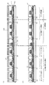
図5は実施形態1で記載した本発明のレジスト剥離工程を連続処理することのできるレジスト剥離装置の全体概略を示す平面図で、被処理基板を1枚ずつ連続的に処理することのできる枚葉処理方式のレジスト剥離装置201を示している。当該レジスト剥離装置201は、複数の被処理基板202を収納可能(通常:20枚程度収納)なローダー側キャリア203と、被処理基板202を処理する為の複数の処理ユニット204〜208と、処理済基板209を収納可能なアンローダー側キャリア210と、被処理基板202を搬送する為の基板搬送ユニット(図示せず)とから成っており、ローダー側キャリア203に収納された被処理基板202が基板搬送ユニット(図示せず)により図中の矢印(→)で示した方向に1枚ずつ順次搬送され、各処理ユニット204〜208で処理される構成になっている。当該レジスト剥離装置201の各処理ユニット204〜208は、被処理基板202上のシリコン系半導体膜の露出した表面にレジスト剥離液に対する保護膜を成膜する為の保護膜成膜ユニット204と、被処理基板202上のレジストパターンを除去する為のレジスト剥離液処理ユニット205と、被処理基板202上に付着しているレジスト剥離液をIPAで置換洗浄する為のIPA処理ユニット206と、被処理基板202を水洗する為の水洗ユニット207と、水洗後の被処理基板202を乾燥する為の乾燥ユニット208とで構成されている(図5参照)。
【0050】
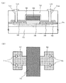
この様な構成のレジスト剥離装置について、各処理ユニットの具体的構成を処理の流れに沿って説明する。最初の処理ユニットである保護膜成膜ユニット204は、被処理基板202の表面に露出しているシリコン系半導体膜とレジスト剥離液が直に接触するのを防止する為、シリコン系半導体膜の表面にレジスト剥離液に対する保護膜を成膜する為の処理ユニットである。当該保護膜としては、レジスト剥離液の吸湿作用により強アルカリ性を示すに至ったレジスト剥離液に対する耐浸食性が必要で、例えば膜厚0.5〜5nm程度のシリコン酸化膜が代表例として挙げられる。この為、保護膜成膜ユニット204の装置構成は、図6に示す様にオゾン含有水や過酸化水素水等の酸化作用を及ぼす薬液を被処理基板202(307)上にスピン添加するスピン添加方式301の装置構成を適用することができる。また、他の装置構成として、図7に示す様に酸素を含む雰囲気中で紫外線を照射することによりオゾンを発生させ、オゾンの酸化作用により被処理基板202(407)上のシリコン系半導体膜の表面を酸化する紫外線照射によるオゾン酸化方式401の装置構成としても良い(図6〜7参照)。
【0051】
スピン添加方式301の装置構成は、図6に示す様に、具体的には処理カップ302と処理カップ302内に配設された回転駆動軸303で軸支されたスピンチャック304とオゾン含有水や過酸化水素水等の酸化作用を及ぼす薬液を供給する為の薬液供給ノズル305と前記薬液を処理カップ302の下側に排液する為の排液管306とから成っており、薬液供給ノズル305からオゾン含有水や過酸化水素水等の酸化作用を及ぼす薬液がスピンチャック304上に載置された被処理基板202(307)に供給され、当該薬液は被処理基板202(307)上に液盛り状態で保持され、所定時間経過後に被処理基板202(307)がスピン乾燥される構成となっている。また、紫外線照射によるオゾン酸化方式401の装置構成は、図7に示す様に、具体的には処理チャンバ402と処理チャンバ402内に配設された基板載置ステージ403と基板載置ステージ403の上方に位置する紫外線照射灯404と処理チャンバ402に酸素を含むガスを供給する為のガス供給管405と紫外線照射灯404に電力を供給する為の電力供給ライン406とから成っており、基板載置ステージ403上に載置された被処理基板202(407)の上方に位置する紫外線照射灯404から紫外線が照射され、同時にガス供給管405から酸素を含むガスが処理チャンバ402内に供給され、紫外線照射により発生したオゾンが処理チャンバ402内に充満することにより、被処理基板202(407)の表面のシリコン系半導体膜が表面酸化される構成となっている(図6〜7参照)。
【0052】
尚、膜厚0.5〜5nm程度のシリコン酸化膜以外の保護膜としては、膜厚0.5〜5nm程度のシリコン酸窒化膜やシリコン窒化膜も候補として挙げられる。シリコン酸窒化膜やシリコン窒化膜の成膜は、露出したシリコン系半導体膜の表面を直接に酸窒化処理したり窒化処理する為、反応性ガスの雰囲気中でのプラズマ処理により酸窒化処理や窒化処理する保護膜成膜ユニット204がある。保護膜成膜ユニット204では、窒素原子と酸素原子を含む反応性ガスの雰囲気中、例えば窒素酸化物の雰囲気中でのプラズマ処理によりシリコン系半導体膜の表面を酸窒化処理し、シリコン酸窒化膜を成膜することが可能となる。また、保護膜成膜ユニット204では、窒素原子を含み酸素原子を含まない反応性ガスの雰囲気中、例えばアンモニアガスの雰囲気中でのプラズマ処理によりシリコン系半導体膜の表面を窒化処理し、シリコン窒化膜を成膜することが可能である。
【0053】
次の処理ユニットであるレジスト剥離液処理ユニット205は、被処理基板202上のエッチングや不純物ドーピングのマスクとなった不要なレジストパターンを除去する為の処理ユニットで、適用するレジスト剥離液としては有機系のレジスト剥離液が一般的である。また、次の処理ユニットであるIPA処理ユニット206は、被処理基板202上に付着しているレジスト剥離液をIPAで置換洗浄する為の処理ユニットである。また、次の処理ユニットである水洗ユニット207は、被処理基板202上に付着しているレジスト剥離液やIPAを水洗により徹底的に洗浄する為の処理ユニットである。これらの処理ユニット205〜207は、当該レジスト剥離装置201に於いては、枚葉処理方式の処理ユニットで構成されており、具体的な装置構成として連続処理槽の装置構成とスピン処理部の装置構成とがある(図5参照)。
【0054】
特に図示しないが、レジスト剥離液処理ユニット205とIPA処理ユニット206に於ける連続処理槽の装置構成は、具体的には連続処理槽内に充填されたレジスト剥離液やIPAに被処理基板202が移動しながら浸漬され所定時間の連続処理が行われる構成となっている。そして、レジスト剥離液処理ユニット205に於いては、連続処理槽に昇温機構が付設されており、連続処理槽内に充填されたレジスト剥離液は60〜90℃程度の所定温度に保持された状態で、被処理基板202が処理される構成となっている。また、水洗ユニット207に於ける連続処理槽の装置構成は、連続処理槽が複数の独立した処理槽に区分され、各処理槽に於いて、被処理基板202が1枚ずつ独立にQDR(Quick-Dump-Rinseの略)方式で水洗処理される構成となっている。尚、上記に記載した連続処理槽の装置構成は単なる一例であり、他の具体的構成も考えられることは言うまでもない(図5参照)。
【0055】
また、レジスト剥離液処理ユニット205とIPA処理ユニット206と水洗ユニット207とに於ける枚葉処理方式のスピン処理部の装置構成は、保護膜成膜ユニット204に於ける図6の装置構成と基本的に同じである。レジスト剥離液処理ユニット205に於いては、60〜90℃程度の所定温度に保持されたレジスト剥離液が、上方に位置する薬液供給ノズルからスピンチャック上に載置された被処理基板202上に供給され、液盛り状態で所定時間保持され、所定時間後に被処理基板202のスピン回転によりレジスト剥離液が被処理基板202の周囲に飛散除去される構成となっている。IPA処理ユニット206に於いては、上方に位置する薬液供給ノズルからスピン回転状態の被処理基板202上にIPAが供給され、被処理基板202上に付着しているレジスト剥離液がIPAで置換洗浄され、所定時間後に被処理基板202のIPAがスピン乾燥される構成となっている。水洗ユニット207に於いては、上方に位置する純水供給ノズルからスピン回転状態の被処理基板202上に純水が供給され、被処理基板202上に付着しているレジスト剥離液やIPAが純水で流水洗浄され、その後被処理基板202がスピン乾燥される構成となっている。尚、水洗ユニット207をスピン処理部で構成する場合は、水洗処理の後に被処理基板202はスピン乾燥される為、後述の乾燥ユニット208は省略可能である(図5参照)。
【0056】
次の処理ユニットである乾燥ユニット208は被処理基板202上に付着している少量の水分を乾燥させる為の処理ユニットで、枚葉処理方式のエアーナイフ乾燥部又はスピン乾燥部で構成されている。スピン乾燥部については、上記のスピン処理部から成る水洗ユニット207と装置構成が同じである為、此処ではエアーナイフ乾燥部の装置構成について記載する。特に図示しないが、エアーナイフ乾燥部から成る乾燥ユニット208に於いては、被処理基板202の表面にエアーナイフノズルからエアーブローが供給され、エアーブローにより付着した水分が乾燥される構成となっている(図5参照)。
【0057】
ところで、上記実施形態に於いては、枚葉処理方式のレジスト剥離装置について具体的に説明したが、本発明のレジスト剥離装置は上記実施形態に限定されるものではなく、その要旨を逸脱しない範囲で種々変更可能であることは言うまでもない。例えば、特に図示しないが、バッチ処理方式のレジスト剥離装置も当然に可能である。この場合、保護膜成膜ユニットは膜厚0.5〜5nm程度のシリコン酸化膜を成膜するバッチ処理方式の処理ユニットとなり、例えばオゾン含有水や過酸化水素水等の酸化作用を及ぼす薬液が充填された処理槽内で複数の被処理基板が一括して処理される装置構成と、酸素を含む雰囲気中で紫外線を照射することによりオゾンを発生させ、オゾンの酸化作用により複数の被処理基板(厳密にはシリコン系半導体膜の表面)が一括して酸化される装置構成とが考えられる。また、膜厚0.5〜5nm程度のシリコン酸窒化膜やシリコン窒化膜を成膜する為のバッチ処理方式のプラズマ処理部から成る保護膜成膜ユニットの装置構成も考えられ、複数の被処理基板がサセプタやボートに載置された状態で、処理チャンバ内に内挿され、反応性ガスの雰囲気中で複数の被処理基板が一括してプラズマ処理される装置構成が挙げられる。尚、反応性ガスとしては、シリコン酸窒化膜を成膜する為の反応性ガスである窒素原子と酸素原子を含む反応性ガス(例えば窒素酸化物)と、シリコン窒化膜を成膜する為の反応性ガスである窒素原子を含み酸素原子を含まない反応性ガス(例えばアンモニアガス)とがある。
【0058】
また、保護膜成膜ユニット以外の処理ユニットであるレジスト剥離液処理ユニットとIPA処理ユニットと水洗ユニットとしては、各々該当する処理液(レジスト剥離液又はIPA又は純水)が充填された処理槽から成るバッチ処理方式の処理ユニットがある。また、バッチ処理方式の乾燥ユニットとしては、複数の被処理基板を一括してスピン乾燥させるスピン乾燥部と複数の被処理基板を一括してIPA蒸気で乾燥させるIPA蒸気乾燥部とがある。
【0059】
以上の様に構成された枚葉処理方式やバッチ処理方式のレジスト剥離装置によると、レジスト剥離液処理前の保護膜成膜処理とレジスト剥離液処理とを連続処理で行うことが可能となり、レジスト剥離工程に於けるシリコン系半導体膜のエッチング損傷を高スループットで確実に防止することができる。TFTで回路構成される半導体表示装置の量産工程に於いては、レジスト剥離工程に於けるシリコン系半導体膜のピンホール状の露出は、何らかのトラブル等により予期せずに生じることが考えられ、この場合にもシリコン系半導体膜のエッチング損傷を高スループットで確実に防止することができる。この為、本発明のレジスト剥離装置は、半導体表示装置の量産工程に於けるTFTの電気特性の安定化及び歩留向上に有効である。
【0060】
〔実施形態3〕
本実施形態では、図8〜14の液晶表示装置の作製工程を示す工程断面図に基づき、GOLD構造TFTとLDD構造TFTとを共に有するアクティブマトリクス型の液晶表示装置の作製工程に本発明のレジスト剥離装置を適用した場合について記載する。尚、本実施形態の液晶表示装置は、TFTの活性層である半導体層に触媒元素を利用して結晶化される結晶質シリコン膜を適用し、LDD構造の画素TFTとGOLD構造のnチャネル型又はpチャネル型駆動回路とを有する場合を例に記載している。
【0061】
先ず、ガラス基板501上にプラズマCVD法により、各々組成比の異なる膜厚50nmの第1層目のシリコン酸窒化膜502aと膜厚100nmの第2層目のシリコン酸窒化膜502bを堆積し、下地膜502を成膜する。尚、此処で用いるガラス基板501としては、石英ガラス又はバリウムホウケイ酸ガラス又はアルミノホウケイ酸ガラス等が有る。次に、前記下地膜502(502aと502b)上に、プラズマCVD法又は減圧CVD法により、膜厚20〜200nm、好ましくは膜厚30〜70nmの非晶質シリコン膜503aを堆積する。本実施形態では、膜厚53nmの非晶質シリコン膜503aをプラズマCVD法で堆積している。この際、非晶質シリコン膜503aの表面は、処理雰囲気中に混入した空気中の酸素の影響により極薄の自然酸化膜(図示せず)が成膜されている。尚、本実施形態ではプラズマCVD法で非晶質シリコン膜503aを堆積しているが、減圧CVD法で堆積しても構わない(図8−A参照)。
【0062】
ところで、非晶質シリコン膜503aの堆積に際しては、空気中に存在する炭素、酸素及び窒素が混入する可能性がある。これらの不純物ガスの混入は、最終的に得られるTFTの特性劣化を引き起こすことが経験的に知られており、前記不純物ガスの混入は結晶化の阻害要因として作用する。従って、前記不純物ガスの混入は徹底的に排除すべきであり、具体的には炭素及び窒素の場合は共に5E17atoms/cm3以下に、酸素の場合は1E18atoms/cm3以下に制御することが好ましい(図8−A参照)。
【0063】
次に、当該基板を希フッ酸で所定時間洗浄することにより、非晶質シリコン膜503aの表面に成膜されている自然酸化膜(図示せず)を除去する。その後、オゾン含有水で所定時間の処理を行うことにより、非晶質シリコン膜503aの表面に膜厚0.5〜5nm程度の清浄な極薄のシリコン酸化膜(図示せず)を成膜する。尚、本実施形態では、オゾン含有水の処理により当該シリコン酸化膜(図示せず)を成膜しているが、過酸化水素水による処理で成膜しても構わない。また、当該シリコン酸化膜(図示せず)は、後に触媒元素溶液であるNi(ニッケル)元素水溶液をスピン添加法で添加する際、Ni元素を均一に付着させる為、非晶質シリコン膜503aに対する濡れ性を改善する目的で成膜される(図8−A参照)。
【0064】
次に、非晶質シリコン膜503a(厳密には、極薄のシリコン酸化膜)の全面に、スピン添加法により結晶化の助長作用を有する触媒元素溶液であるNi元素水溶液を添加する。本実施形態では、Ni化合物であるニッケル酢酸塩を純水に溶解し、重量換算で10ppmの濃度に調整したものをNi元素水溶液として使用しており、非晶質シリコン膜503a(厳密には極薄のシリコン酸化膜)の全面にNi含有層(図示せず)を均一に付着させている(図8−A参照)。
【0065】
次に、非晶質シリコン膜503a中の含有水素量を5atom%以下に制御する為、非晶質シリコン膜503a中の含有水素の脱水素化処理を行う。当該脱水素化処理は、ファーネス炉を使用して窒素雰囲気中での450℃−1時間の熱処理により行われる。その後、ファーネス炉内で550℃−4時間の熱処理を行うことにより、非晶質シリコン膜503aの結晶化を促進し、膜厚50nmの結晶質シリコン膜503bを成膜する。引き続き、得られた結晶質シリコン膜503bの結晶性を更に改善させる為、パルス発振型のKrFエキシマレーザー(波長248nm)照射による結晶化を行う。尚、本明細書に於いては、触媒元素であるNi元素を利用して結晶化される多結晶シリコン膜を通常の多結晶シリコン膜と区別する為に、結晶質シリコン膜と称している。此処で、多結晶とせずに結晶質と称している理由は、通常の多結晶シリコン膜と比較し、結晶粒が概略同一方向に配向しており、高い電界効果移動度を有する等の特徴がある為、多結晶シリコン膜と区別する趣旨である(図8−A参照)。
【0066】
次に、希フッ酸洗浄とオゾン含有水洗浄による所定時間のチャネルドープ前洗浄を行い、結晶質シリコン膜503bの表面に膜厚0.5〜5nm程度の清浄な極薄のシリコン酸化膜(図示せず)を再び成膜する。当該シリコン酸化膜(図示せず)は、チャネルドープ処理の際に水素イオン(イオン源であるジボラン(B2H6)と水素との混合ガスから発生)で結晶質シリコン膜503bがエッチングされるのを防止する為のものである。その後、nチャネル型TFT及びpチャネル型TFTのしきい値電圧を制御する為、ドーピング装置を使用して第1のドーピング処理であるチャネルドープ処理を行う。チャネルドープ処理は、低ドーズ量のp型不純物であるB(即ち、ボロン)元素を基板全面にドーピングすることで行われる。この際のドーピング条件としては、イオン源にジボラン(B2H6)希釈率0.01〜1%濃度のジボラン(B2H6)/水素(H2)を使用し、加速電圧5〜30kVでドーズ量8×1013〜2×1015atoms/cm2が考えられ、本実施例では結晶質シリコン膜503b中のB濃度を1×1017atoms/cm3程度とする為、ジボラン(B2H6)希釈率0.1%濃度のジボラン(B2H6)/水素(H2),加速電圧15kV,ドーズ量4×1014atoms/cm2のドーピング条件でB元素をドーピングしている(図8−B参照)。
【0067】
次に、チャネルドープ処理の前処理として成膜した極薄のシリコン酸化膜(図示せず)を希フッ酸で処理することにより、当該シリコン酸化膜(図示せず)を除去する。その後、オゾン含有水で所定時間の処理を行うことにより、結晶質シリコン膜503bの表面に膜厚0.5〜5nm程度の極薄のシリコン酸化膜504a〜508aを再び成膜する。当該シリコン酸化膜504a〜508aは、次に形成するレジストパターンの密着性改善の為、及び結晶質シリコン膜503bの疎水性の改善と汚染防止の為、及び結晶質シリコン膜503bの表面の清浄度を保持することにより界面準位の低減を図る為等の理由で成膜されるが、有機系のレジスト剥離液からのエッチング損傷の防止機能についても勿論有している。尚、本実施形態では、膜厚0.5〜5nm程度のシリコン酸化膜504a〜508aをオゾン含有水による処理で成膜しているが、過酸化水素水で処理しても良いし、酸素を含む雰囲気中で紫外線を照射することによりオゾンを発生させ、オゾンによる酸化作用で結晶質シリコン膜503bの表面を酸化しても良い。その後、通常のフォトリソグラフィ処理により、所定寸法のレジストパターン(図示せず)を形成する(図8−B参照)。
【0068】
次に、当該レジストパターン(図示せず)をマスクに結晶質シリコン膜503bとその表層膜であるシリコン酸化膜504a〜508aをドライエッチング処理し、膜厚50nmの結晶質シリコン膜503bから成る島状の半導体層504〜508を形成する。この半導体層504〜508はTFTの活性層となる島状の領域で、後にTFTのソース領域とドレイン領域が形成される領域である。ドライエッチング処理の際、RIE型のドライエッチング装置を使用し、エッチングガスであるCF4とO2のガス流量比が50:45のエッチング条件でドライエッチング処理しており、レジスト後退方によるテーパーエッチング処理が行われている。この為、被エッチング膜である半導体層504〜508の側壁部には、特に便宜上図示してないが、順テーパー形状が形成されている(図中では便宜上矩形状で表記)。また、順テーパー形状の側壁部は、エッチングガスに酸素が含まれている為、ドライエッチング時の側壁保護ポリマーの付着は殆ど無く、結晶質シリコン膜503bの表面が露出した状態(又は若干のシリコン酸化膜の成膜もあり得る)になっている。尚、半導体層504〜508を順テーパー形状に形成する理由は、後工程で成膜されるゲート絶縁膜やゲート電極膜の段差部での被覆性を改善する為である(図8−B参照)。
【0069】
次に、ドライエッチング後のレジストパターン(図示せず)を除去する為、酸素プラズマ処理であるアッシング処理を行う。アッシング処理は、レジストパターンの半分程度をアッシングするハーフアッシング方式を採用している。この為、アッシング処理後のレジストパターン(図示せず)は、半分程度に膜減りが進み、レジストパターン形状が変形している。このアッシング処理の際、順テーパー形状をしている半導体層504〜508の側壁部には、結晶質シリコン膜503bが露出している為、膜厚0.5〜5nm程度のシリコン酸化膜504b〜508bが成膜される。当該シリコン酸化膜504b〜508bは、次工程のレジスト剥離液処理時のレジスト剥離液からのエッチング損傷を防止する機能を有するものとがある(図8−B参照)。
【0070】
次に、残ったレジストパターン(図示せず)を完全に除去する為、本発明のレジスト剥離装置を使用してレジスト剥離工程を行う。本発明のレジスト剥離装置はレジスト剥離液処理の前に保護膜成膜処理を行うことが可能であるが、当該レジスト剥離工程の場合は、結晶質シリコン膜503bから成る半導体層504〜508の表面と側面に膜厚0.5〜5nm程度のシリコン酸化膜504a〜508a,504b〜508bが既に成膜されている為、半導体層504〜508に対する保護膜の成膜処理は不要である。この場合は、レジスト剥離装置の処理プログラムを保護膜成膜処理の無いプログラムに変更して処理することになり、レジスト剥離工程の一層の高スループット化を図ることが可能である。従って、この場合の当該レジスト剥離装置によるレジスト剥離工程の具体的処理は、レジスト剥離液処理とIPA洗浄処理と水洗処理と乾燥処理とから成る連続処理で処理されることになる。尚、レジスト剥離液処理の後、連続的にIPA洗浄処理が行われるが、当該IPA洗浄処理は省略しても弊害が無い場合に限り省略することも可能である。但し、当該IPA洗浄処理は基板表面近傍での水洗時のレジスト剥離液と純水との混合液の生成を防止する作用があり、水分の混入によるレジスト剥離液の強アルカリ性化を防止する作用がある為、一般的にはIPA洗浄処理を導入した方が好ましい(図8−B参照)。
【0071】
次に、当該基板を希フッ酸で所定時間洗浄することにより、結晶質シリコン膜503bから成る半導体層504〜508の表面と側壁部に成膜されている膜厚0.5〜5nm程度のシリコン酸化膜504a〜508a,504b〜508bを除去する。その後、半導体層504〜508を被覆する様に、膜厚30〜200nm、好ましくは膜厚80〜130nmのシリコン酸化膜又はシリコン酸窒化膜から成るゲート絶縁膜509をプラズマCVD法又は減圧CVD法により堆積する。本実施形態では、膜厚100nmのシリコン酸化膜から成るゲート絶縁膜509をプラズマCVD法で堆積している。尚、ゲート絶縁膜509の膜厚は、後工程で成膜する上層のゲート電極膜からの応力を回避する為、80nm以上の膜厚が必要であることが知られており、この点を考慮して設定している(図9−A参照)。
【0072】
次に、ゲート電極用の電極材料を堆積する為、スパッタ法により膜厚200〜600nm、好ましくは膜厚300〜600nmのアルミニウム系合金膜、又は高融点金属と高融点金属窒化物との積層膜を堆積する。本実施形態では、第1層ゲート電極膜510として膜厚30nmのTaN膜を堆積し、その後第2層ゲート電極膜511として膜厚370nmのW膜とを堆積している。尚、第1層ゲート電極膜510であるTaN膜の膜厚は、ドライエッチング時のテーパー形状領域に於ける残膜厚の制御性、及びスルードープ法によりTaN膜を通過させて不純物元素をドーピングする際のドーピング特性の両方を考慮して設定している。また、第2層ゲート電極膜511であるW膜の膜厚は、不純物元素をドーピングする際のW膜のチャネリング現象を防止する為、340nm以上の膜厚が必要なことが知られており、この点を考慮して設定している(図9−A参照)。
【0073】
次に、通常のフォトリソグラフィ処理を行うことにより、上記の金属積層膜上にゲート電極と保持容量用電極とソース配線等を形成する為の所定寸法のレジストパターン(図示せず)を形成する。その後、レジストパターン(図示せず)をマスクに、膜厚30nmのTaN膜から成る第1層ゲート電極膜510と膜厚370nmのW膜から成る第2層ゲート電極膜511とから成る金属積層膜をドライエッチング処理する。当該ドライエッチング処理により、第1層ゲート電極512c〜515cと第2層ゲート電極512b〜515bとから成る所定寸法のゲート電極を形成し、同時に第1層保持容量電極516cと第2層保持容量電極516bとから成る所定寸法の保持容量電極、第1層ソース配線用電極517cと第2層ソース配線用電極517bとから成る所定寸法のソース配線用電極を形成する。当該ドライエッチング工程に於いて、第2層電極512b〜517b(第2層ゲート電極512b〜515bと第2層保持容量電極516bと第2層ソース配線用電極517bとから成る電極の総称)は第1層電極512c〜517c(第1層ゲート電極512c〜515cと第1層保持容量電極516cと第1層ソース配線用電極517cとから成る電極の総称)よりチャネル方向の寸法が短く形成されている。また、第2層電極512b〜517bからの露出領域に該当する第1層電極512c〜517cは、端部に近づくにつれ徐々に薄膜化したテーパー形状に形成されている。尚、現像後のレジストパターン(図示せず)は、ドライエッチング時の膜減りによりレジストパターン512a〜517aの形状となり、ゲート絶縁膜509はドライエッチング時の膜減りにより、ゲート絶縁膜518の形状に変形している(図9−B参照)。
【0074】
次に、ドライエッチング後のレジストパターン512a〜517aを除去する為、ハーフアッシング方式によるアッシング処理を行う。当該アッシング処理でレジストパターン512a〜517aを半分程度にアッシング除去した後、残ったレジストパターン(図示せず)を完全に除去する為、本発明のレジスト剥離装置を使用してレジスト剥離工程を行う。本発明のレジスト剥離装置はレジスト剥離液処理の前に保護膜成膜処理を行うことが可能であるが、当該レジスト剥離工程の場合は、半導体層504〜508を被覆する様にゲート絶縁膜518が存在している為、半導体層504〜508とレジスト剥離液が直に接触することは通常あり得ず、保護膜の成膜処理は不要である。この場合は、レジスト剥離装置の処理プログラムを保護膜成膜処理の無いプログラムに変更して処理することになり、レジスト剥離工程の一層の高スループット化を図ることが可能である。従って、この場合の当該レジスト剥離装置によるレジスト剥離工程の具体的処理は、レジスト剥離液処理とIPA洗浄処理と水洗処理と乾燥処理とから成る連続処理で処理される。尚、レジスト剥離液処理の後、連続的にIPA洗浄処理が行われるが、当該IPA洗浄処理は省略しても弊害が無い場合に限り省略することも可能である。但し、当該IPA洗浄処理は基板表面近傍での水洗時のレジスト剥離液と純水との混合液の生成を防止する作用があり、水分の混入によるレジスト剥離液の強アルカリ性化を防止する作用がある為、一般的にはIPA洗浄処理を導入した方が好ましい(図10−A参照)。
【0075】
次に、ドーピング装置を使用して、第1層電極512c〜516cをマスクに第2のドーピング処理であるP元素から成る低ドーズ量のn型不純物をドーピングする。当該第2のドーピング処理により、第1層電極512c〜516cの外側の領域に対応する半導体層504〜508にn型不純物の低濃度不純物領域(n−−領域)519〜523が形成される。この際、低濃度不純物領域(n−−領域)519〜523の形成に於いては、所謂スルードープ法により上層膜であるゲート絶縁膜518を介してドーピングしている。尚、ドーピング条件としては、イオン源にホスフィン(PH3)希釈率3〜20%濃度のホスフィン(PH3)/水素(H2)を使用し、加速電圧30〜90kVでドーズ量6×1012〜1.5×1014atoms/cm2が考えられるが、本実施形態ではホスフィン(PH3)希釈率5%濃度のホスフィン(PH3)/水素(H2),加速電圧50kV,ドーズ量3×1013atoms/cm2のドーピング条件でドーピングしている(図10−B参照)。
【0076】
次に、通常のフォトリソグラフィ処理により、不純物をドーピング処理する為のマスクであるレジストパターン524〜525を形成する。当該レジストパターン524〜525は、GOLD構造の駆動回路606であるpチャネル型TFT602とLDD構造の画素TFT604の作製領域に形成され、GOLD構造の駆動回路606であるnチャネル型TFT601,603並びに保持容量605の作製領域には形成されない。この際、GOLD構造のpチャネル型TFT602の作製領域に於いては、レジストパターン524の端部が、半導体層505の外側に位置する様に、即ち半導体層505を完全に被覆する様に形成される。また、LDD構造の画素TFT604の作製領域に於いては、レジストパターン525の端部が半導体層507の内側で第1層ゲート電極515cから所定の距離だけ外側に位置する様に、即ち第1層ゲート電極515cの端部からLoff領域(詳細は後の工程で説明)の分だけ外側に位置する様に形成される(図11−A参照)。
【0077】
次に、ドーピング装置を使用して、第3のドーピング処理であるP元素から成る高ドーズ量のn型不純物をドーピングする。この際、GOLD構造の駆動回路606であるnチャネル型TFT601,603の作製領域に於いては、第1層ゲート電極512c,514cの外側に対応する半導体層504,506には、既にn型不純物の低濃度不純物領域(n−−領域)519,521が形成されているが、その上からn型不純物の高濃度不純物領域(n+領域)526,528が形成され、同時に第1層ゲート電極512c,514cの第2層ゲート電極512b,514bからの露出領域に対応する半導体層504,506に、n型不純物の低濃度不純物領域(n−領域)527,529が形成される。この様にして形成される高濃度不純物領域(n+領域)526,528はGOLD構造のソース領域又はドレイン領域としての機能を有し、低濃度不純物領域(n−領域)527,529はGOLD構造のLov領域(ゲート電極とオーバーラップしている電界緩和領域のこと)である電界緩和領域としての機能を有することになる。また、保持容量605の作製領域に於いても、同様にn型不純物の高濃度不純物領域(n+領域)532と低濃度不純物領域(n−領域)533が形成される。此処で形成されたn型不純物の高濃度不純物領域(n+領域)532と低濃度不純物領域(n−領域)533は、当該領域がTFTでなく保持容量605の作製領域である為、容量形成用電極の片側としての機能を有している(図11−A参照)。
【0078】
一方、LDD構造の画素TFT604の作製領域に於いては、当該第3のドーピング処理により、レジストパターン525の外側に対応する半導体層507にn型不純物の高濃度不純物領域(n+領域)530が形成される。当該半導体層507には、既にn型不純物の低濃度不純物領域(n−−領域)522が形成されているが、高濃度不純物領域(n+領域)530の形成に伴い、当該低濃度不純物領域(n−−領域)522は、高濃度不純物領域(n+領域)530と結果として形成される低濃度不純物領域(n−−領域)531とに区分されることになる。この様にして形成される高濃度不純物領域(n+領域)530はLDD構造のソース領域又はドレイン領域としての機能を有し、低濃度不純物領域(n−−領域)531はLDD構造のLoff領域(ゲート電極とオーバーラップしてない電界緩和領域のこと)である電界緩和領域としての機能を有することになる。尚、ドーピング条件としては、イオン源にホスフィン(PH3)希釈率3〜20%濃度のホスフィン(PH3)/水素(H2)を使用し、加速電圧30〜90kVでドーズ量6×1014〜1.5×1016atoms/cm2が考えられるが、本実施形態ではホスフィン(PH3)希釈率5%濃度のホスフィン(PH3)/水素(H2),加速電圧65kV,ドーズ量3×1015atoms/cm2のドーピング条件でドーピングしている(図11−A参照)。
【0079】
上記の高濃度不純物領域(n+領域)526,528,530,532と低濃度不純物領域(n−領域)527,529,533は、上層膜を介してドーピングする所謂スルードープ法で形成されている。スルードープ法とは上層膜を介して目的物質層に不純物をドーピングするドーピング法のことで、上層膜の膜質と膜厚に依存して目的物質層の不純物濃度を変化できる特徴がある。従って、同一のドーピング条件で不純物をドーピングするにも拘わらず、上層膜がイオン阻止能の小さいゲート絶縁膜518で構成されている領域に高濃度不純物領域(n+領域)526,528,530,532を形成し、上層膜がイオン阻止能の大きい第1層電極(TaN膜)512c,514c,516cとゲート絶縁膜518との積層膜で構成されている領域に低濃度不純物領域(n−領域)527,529,533を同時に形成することが可能となっている(図11−A参照)。
【0080】
尚、GOLD構造の駆動回路606であるnチャネル型TFT601,603の作製領域に於いては、上記の高濃度不純物領域(n+領域)526,528と低濃度不純物領域(n−領域)527,529の形成に伴い、半導体層504,506に於ける第2層ゲート電極512b,514bと重なる領域に、TFTのチャネル領域が画定されることになる。また、同様にして、LDD構造の画素TFT604の作製領域に於いて、半導体層507に於ける第1層ゲート電極515cと重なる領域に、TFTのチャネル領域が画定されることになる(図11−A参照)。
【0081】
次に、ドーピング処理後のレジストパターン524〜525を除去する為、ハーフアッシング方式によるアッシング処理を行う。当該アッシング処理でレジストパターン524〜525を半分程度にアッシング除去した後、残ったレジストパターン(図示せず)を完全に除去する為、本発明のレジスト剥離装置を使用してレジスト剥離工程を行う。尚、レジスト剥離工程の詳細は、上記のドライエッチング処理後の保護膜成膜処理の無いレジスト剥離工程と同様である為、此処では記載を省略する。その後、通常のフォトリソグラフィ処理により、不純物をドーピング処理する為のマスクであるレジストパターン534〜536を形成する。この際、当該レジストパターン534〜536は、GOLD構造の駆動回路606であるpチャネル型TFT602と保持容量605の作製領域を開口する様に形成される(図11−B参照)。
【0082】
次に、ドーピング装置を使用して、第4のドーピング処理であるB元素から成る高ドーズ量のp型不純物をスルードープ法でドーピングする。当該第4のドーピング処理により、GOLD構造の駆動回路606であるpチャネル型TFT602の作製領域に於いては、第1層ゲート電極513cの外側に対応する半導体層505に、p型不純物の高濃度不純物領域(p+領域)537が形成される。また、第1層ゲート電極513cの第2層ゲート電極513bからの露出領域に対応する半導体層505に、p型不純物の低濃度不純物領域(p−領域)538が同時に形成される。この様にして形成される高濃度不純物領域(p+領域)537はGOLD構造のソース領域又はドレイン領域としての機能を有し、低濃度不純物領域(p−領域)538はGOLD構造のLov領域(ゲート電極とオーバーラップしている電界緩和領域のこと)である電界緩和領域としての機能を有することになる。一方、保持容量605の作製領域に於いても、同様に、容量形成用電極の片側として機能する高濃度不純物領域(p+領域)539と低濃度不純物領域(p−領域)540とが形成されている(図11−B参照)。
【0083】
ところで、pチャネル型TFT602の作製領域に於けるp型不純物の高濃度不純物領域(p+領域)537には、既にn型不純物の低濃度不純物領域(n−−領域)520が形成されているが、n型不純物の濃度以上のp型不純物がドーピングされる為、全体としてp型の導電型を有する高濃度不純物領域(p+領域)537が形成されることになる。また、保持容量605の作製領域に於いても、既にn型不純物の高濃度不純物領域(n+領域)532と低濃度不純物領域(n−領域)533とが形成されているが、n型不純物の濃度以上のp型不純物がドーピングされる為、全体としてp型の導電型を有する高濃度不純物領域(p+領域)539と低濃度不純物領域(p−領域)540とが形成されている。尚、p型不純物の高濃度不純物領域(p+領域)537,539と低濃度不純物領域(p−領域)538,540は、n型不純物領域の場合と同様に、上層膜の膜質や膜厚の違いを利用してスルードープ法により同時に形成されている。また、この際のドーピング条件としては、イオン源にジボラン(B2H6)希釈率3〜20%濃度のジボラン(B2H6)/水素(H2)を使用し、加速電圧60〜100kVでドーズ量4×1015〜1×1017atoms/cm2が考えられるが、本実施形態ではジボラン(B2H6)希釈率5%濃度のジボラン(B2H6)/水素(H2),加速電圧80kV,ドーズ量2×1016atoms/cm2のドーピング条件でドーピングしている(図11−B参照)。
【0084】
次に、ドーピング処理後のレジストパターン534〜536を除去する為、ハーフアッシング方式によるアッシング処理を行う。当該アッシング処理でレジストパターン534〜536を半分程度にアッシング除去した後、残ったレジストパターン(図示せず)を完全に除去する為、本発明のレジスト剥離装置を使用してレジスト剥離工程を行う。尚、レジスト剥離工程の詳細は、上記のドライエッチング処理後の保護膜成膜処理の無いレジスト剥離工程と同様である為、此処では記載を省略する。その後、膜厚50〜300nm、好ましくは膜厚100〜200nmのシリコン酸窒化膜又はシリコン窒化膜から成る第1の層間絶縁膜541をプラズマCVD法により堆積する。本実施形態では、膜厚150nmのシリコン窒化膜から成る第1の層間絶縁膜541をプラズマCVD法により堆積している。しかる後に、半導体層504〜508にドーピングされたn型不純物(P元素)又はp型不純物(B元素)の熱活性化の為、ファーネス炉に於いて、600℃−12時間の熱処理を行う。当該熱処理は、n型又はp型不純物の熱活性化処理の為に行うものであるが、ゲート電極の真下に位置するチャネル領域に存在する触媒元素(Ni元素)を前記不純物によりゲッタリングする目的も兼ねている。尚、第1の層間絶縁膜541の堆積前に当該熱活性化処理を行っても良いが、ゲート電極等の配線材料の耐熱性が弱い場合は、第1の層間絶縁膜541の堆積後に行う方が好ましい。当該熱処理に続いて、半導体層504〜508のダングリングボンドを終端させる為、410℃−1時間の水素化処理を水素3%含有の窒素雰囲気中で行う(図12−A参照)。
【0085】
次に、前記第1の層間絶縁膜541の上に、膜厚0.7〜3μm、好ましくは膜厚1〜2μmのアクリル樹脂膜から成る第2の層間絶縁膜542を成膜する。本実施形態では、膜厚1.6μmのアクリル樹脂膜から成る第2の層間絶縁膜542を成膜している。当該アクリル樹脂膜の成膜は、スピン塗布法でアクリル樹脂膜を塗布した後、オーブンベーク炉で熱処理することにより成膜される。その後、通常のフォトリソグラフィ処理により、アクリル樹脂膜から成る第2の層間絶縁膜542上に所定寸法のコンタクトホールを形成する為のレジストパターン543aを形成する(図12−B参照)。
【0086】
次に、レジストパターン543aをマスクに、アクリル樹脂膜から成る第2の層間絶縁膜542とシリコン窒化膜から成る第1の層間絶縁膜541とシリコン酸化膜から成るゲート絶縁膜518の積層膜をドライエッチング処理する。当該ドライエッチング処理により、第2の層間絶縁膜542と第1の層間絶縁膜541とゲート絶縁膜518とを貫通する様に、所定寸法のコンタクトホール544が形成される。この際、当該ドライエッチング処理工程に於いては、酸素とCF4のガス流量比が19:1のガス混合条件でのドライエッチング処理により第2の層間絶縁膜542であるアクリル樹脂膜がエッチングされ、酸素とCF4のガス流量比が1:1のガス混合条件でのドライエッチング処理により第1の層間絶縁膜541であるシリコン窒化膜がエッチングされ、CHF3ガスによるドライエッチング処理によりゲート絶縁膜518であるシリコン酸化膜がエッチング処理される。この様に、ドライエッチング処理の最終段階で、CHF3ガスプラズマが適用されている為、コンタクトホール544の底部に存在する結晶質シリコン膜503bから成る半導体層504〜508に対し高選択比のドライエッチング処理が実現されている。また、ドライエッチング後に於いては、レジストパターン543aは酸素(厳密には5%のCF4含有)プラズマ処理で大幅に膜減りが進んだ結果、レジストパターン543bの形状に変形している。尚、コンタクトホール544は、n型不純物の高濃度不純物領域(n+領域)526,528,530及びp型不純物の高濃度不純物領域(p+領域)537,539、更にはソース配線として機能するソース配線用電極517bc(第1層ソース配線用電極517cと第2層ソース配線用電極517bとで構成)に接続する様に形成されている(図13−A参照)。
【0087】
次に、ドライエッチング処理後の不要なレジストパターン543bを除去する為、本発明のレジスト剥離装置を使用してレジスト剥離工程を行う。此処では、第2の層間絶縁膜542に有機系のアクリル樹脂膜が適用されている為、レジスト除去処理にアッシング工程を導入することができず、レジスト剥離工程のみでレジストパターンの除去処理を行っている。本発明のレジスト剥離装置は、レジスト剥離液処理の前に膜厚0.5〜5nm程度のシリコン酸化膜から成る保護膜の成膜処理を行うことが可能で、当該レジスト剥離工程に於いては、保護膜成膜処理を有する処理条件でレジスト剥離工程を処理することになる。当該レジスト剥離装置によるレジスト剥離工程は、レジスト剥離液処理前の保護膜成膜処理とレジスト剥離液処理とIPA洗浄処理と水洗処理と乾燥処理とから成っており、レジスト剥離液処理前の保護膜成膜である膜厚0.5〜5nm程度の極薄のシリコン酸化膜成膜処理とレジスト剥離液処理とを連続処理で行うことが可能である。従って、レジスト剥離液処理前に、コンタクトホール544の底部に露出している結晶質シリコン膜503bから成る半導体層504〜508の表面にレジスト剥離液に対する保護膜545である膜厚0.5〜5nm程度の極薄のシリコン酸化膜を成膜することができ、レジスト剥離液による結晶質シリコン膜503bのエッチング損傷を高スループットで確実に防止することが可能である。尚、此処で使用するレジスト剥離液としては、例えば特開2000−241991号公報、特開2001−183849号公報、特開2001−188363号公報、特開2001−209190号公報等に開示されている様な結晶質シリコン膜に対するエッチング損傷の少ないレジスト剥離液の方が好ましい。但し、結晶質シリコン膜に対するエッチング損傷の少ないレジスト剥離液は、肝心のレジスト剥離性能に問題がある場合が多く、レジスト剥離性能とシリコン系半導体膜に対するエッチング損傷防止性能とを共に満足する様なレジスト剥離液が好適で、当該レジスト剥離液を適用することが好ましい。また、レジスト剥離液処理の後、連続的にIPA洗浄処理が行われるが、当該IPA洗浄処理は省略しても弊害が無い場合に限り省略することも可能である。但し、当該IPA洗浄処理は基板表面近傍での水洗時のレジスト剥離液と純水との混合液の生成を防止する作用があり、基板上に露出している結晶質シリコン膜や金属配線へのエッチング損傷防止に有利に作用する為、一般的にはIPA洗浄処理を導入した方が好ましい(図13−B参照)。
【0088】
次に、スパッタ前洗浄として希フッ酸処理を行い、コンタクトホール544の底部に露出している結晶質シリコン膜503b表面の保護膜(シリコン酸化膜)545を除去する。その後、Ti(100nm)/Al(350nm)/Ti(100nm)の3層膜から成る金属積層膜をスパッタ法により堆積する。尚、当該金属積層膜に於いて、膜厚100nmの1層目のTi膜はコンタクト抵抗の低抵抗化とシリコンとアルミニウムの相互拡散を防止する目的で堆積され、膜厚100nmの3層目のTi膜はアルミニウム配線表面のヒロックを防止する目的で堆積されている。金属積層膜を堆積した後、通常のフォトリソグラフィ処理により、金属積層膜上に所定寸法の配線形成用のレジストパターン(図示せず)を形成する(図14−A参照)。
【0089】
次に、塩素系のエッチングガスを使用してドライエッチング処理を行うことにより、所定寸法の金属積層膜配線546〜551と接続電極552,554,555とゲート配線553とを同時に形成する。金属積層膜配線546〜551は、駆動回路606の高濃度不純物領域(n+領域)526,528と高濃度不純物領域(p+領域)537とに電気的に接続する様に形成されている。また、接続電極552は、画素TFT604の高濃度不純物領域(n+領域)530とソース配線として機能する第2層ソース配線用電極517bとを電気的に接続する様に形成されている。また、接続電極554は、画素TFT604の高濃度不純物領域(n+領域)530と電気的に接続する様に形成されており、接続電極555は保持容量605の高濃度不純物領域(p+領域)539と電気的に接続する様に形成されている。また、ゲート配線553は、画素TFT604の複数の第2層ゲート電極515bを電気的に接続する様に形成されている。ドライエッチング処理の後、不要なレジストパターン(図示せず)を除去する為、本発明のレジスト剥離装置を使用してレジスト剥離工程を行う。此処では、第2の層間絶縁膜542に有機系のアクリル樹脂膜が適用されている為、レジスト除去処理にアッシング工程を導入することができず、レジスト剥離工程のみでレジストパターンの除去処理を行っている。尚、レジスト剥離工程の詳細は、上記のドライエッチング処理後のレジスト剥離工程と同様である為、此処では記載を省略する(図14−A参照)。
【0090】
次に、膜厚80〜130nm、好ましくは膜厚100〜120nmの透明導電膜であるITO(Indium−Ti−Oxideの略)膜をスパッタ法により堆積する。本実施形態では、膜厚110nmのITO膜をスパッタ法により堆積している。その後、通常のフォトリソグラフィ処理により、所定寸法の画素電極用のレジストパターン(図示せず)を形成する。しかる後、関東化学(株)製の商品名「ITO−04N」のエッチング液を使用して、ウェットエッチング処理を行う。当該ウェットエッチング処理により、ITO膜から成る所定寸法の画素電極556が接続電極554,555に接続される様に形成される。画素電極556は、接続電極554を介して、画素TFT604のソース領域又はドレイン領域として機能する高濃度不純物領域(n+領域)530と電気的に接続されており、更に接続電極555を介して、保持容量605の高濃度不純物領域(p+領域)539とも電気的に接続されている。ウェットエッチング処理の後、不要なレジストパターン(図示せず)を除去する為、本発明のレジスト剥離装置を使用してレジスト剥離工程を行う。此処では、第2の層間絶縁膜542に有機系のアクリル樹脂膜が適用されている為、レジスト除去処理にアッシング工程を導入することができず、レジスト剥離工程のみでレジストパターン(図示せず)の除去処理を行っている。尚、レジスト剥離工程の詳細は、上記のドライエッチング処理後の保護膜成膜処理の無いレジスト剥離工程と同様である為、此処では記載を省略する(図14−B参照)。
【0091】
以上の様に、アクティブマトリクス型液晶表示装置のレジスト剥離工程に本発明のレジスト剥離装置を適用することにより、レジスト剥離液による結晶質シリコン膜から成る半導体層のエッチング損傷を高スループットで確実に防止することが可能である。尚、レジスト剥離工程によっては、結晶質シリコン膜の露出が全く有り得ない工程もあり、レジスト剥離装置の処理プログラムを保護膜成膜処理の無いプログラムに変更して処理することが可能である。この様に本発明のレジスト剥離装置は、レジスト剥離工程により保護膜成膜処理の有無をプログラム設定で簡単に変更可能で、高スループットを維持した状態で、結晶質シリコン膜から成る半導体層のエッチング損傷を確実に防止することが可能である。尚、本実施形態に於いては、アクティブマトリクス型液晶表示装置の作製方法について具体的に説明したが、アクティブマトリクス型の有機EL表示装置の作製方法にも適用可能であることは言うまでもない。
【0092】
〔実施形態4〕
本実施形態では、本発明のレジスト剥離工程やレジスト剥離装置を適用して作製される半導体表示装置を組み込んだ電子機器の具体例について記載する。当該半導体表示装置としては、アクティブマトリクス型の液晶表示装置及びEL表示装置等があり、様々な電子機器の表示部に適用されている。此処では、半導体表示装置が表示部に適用された電子機器の具体例を図16〜18に基づき記載する。
【0093】
尚、半導体表示装置が表示部に適用された電子機器としては、ビデオカメラとデジタルカメラとプロジェクター(リア型又はフロント型)とヘッドマウントディスプレイ(ゴーグル型ディスプレイ)とゲーム機とカーナビゲーションとパーソナルコンピュータと携帯情報端末(モバイルコンピュータ,携帯電話,電子書籍等)等が挙げられる。
【0094】
図16−Aは、本体1001と映像入力部1002と表示装置1003とキーボード1004とで構成されたパーソナルコンピューターである。当該表示装置1003及び他の回路に、本発明の半導体表示装置を適用することができる。
【0095】
図16−Bはビデオカメラであり、本体1101と表示装置1102と音声入力部1103と操作スイッチ1104とバッテリー1105と受像部1106とで構成される。当該表示装置1102及び他の回路に、本発明の半導体表示装置を適用することができる。
【0096】
図16−Cはモバイルコンピュータ(モービルコンピュータ)であり、本体1201とカメラ部1202と受像部1203と操作スイッチ1204と表示装置1205とで構成される。当該表示装置1205及び他の回路に、本発明の半導体表示装置を適用することができる。
【0097】
図16−Dはゴーグル型ディスプレイであり、本体1301と表示装置1302とアーム部1303とで構成される。当該表示装置1302及び他の回路に、本発明の半導体表示装置を適用することができる。
【0098】
図16−Eはプログラムを記録した記録媒体(以下、記録媒体と略記)に用いるプレーヤーであり、本体1401と表示装置1402とスピーカー部1403と記録媒体1404と操作スイッチ1405とで構成される。尚、この装置は記録媒体としてDVD及びCD等が用いられ、音楽鑑賞又はゲーム又はインターネットに利用可能である。当該表示装置1402及び他の回路に、本発明の半導体表示装置を適用することができる。
【0099】
図16−Fは携帯電話であり、表示用パネル1501と操作用パネル1502と接続部1503と表示部1504と音声出力部1505と操作キー1506と電源スイッチ1507と音声入力部1508とアンテナ1509とで構成される。表示用パネル1501と操作用パネル1502は、接続部1503で接続されている。表示用パネル1501の表示部1504が設置されている面と操作用パネル1502の操作キー1506が設置されている面との角度θは、接続部1503に於いて任意に変えることができる。尚、当該表示部1504に、本発明の半導体表示装置を適用することができる(図16参照)。
【0100】
図17−Aはフロント型プロジェクターであり、光源光学系及び表示装置1601とスクリーン1602とで構成される。当該表示装置1601及び他の回路に、本発明の半導体表示装置を適用することができる。
【0101】
図17−Bはリア型プロジェクターであり、本体1701と光源光学系及び表示装置1702とミラー1703〜1704とスクリーン1705とで構成される。当該表示装置1702及び他の回路に、本発明の半導体表示装置を適用することができる。
【0102】
尚、図17−Cは、図17−Aに示された光源光学系及び表示装置1601と図17−Bに示された光源光学系及び表示装置1702に於ける構造の一例を示した図である。光源光学系及び表示装置1601,1702は、光源光学系1801とミラー1802,1804〜1806とダイクロイックミラー1803と光学系1807と表示装置1808と位相差板1809と投射光学系1810とで構成される。投射光学系1810は、投射レンズを備えた複数の光学レンズで構成される。この構成は、表示装置1808を3個使用している為、三板式と呼ばれている。また、同図の矢印で示した光路に於いて、光学レンズ及び偏光機能を有するフィルム又は位相差を調整する為のフィルム又はIRフィルム等を適宜に配設しても良い。
【0103】
図17−Dは、図17−Cに於ける光源光学系1801の構造の一例を示した図である。本実施例に於いては、光源光学系1801はリフレクター1811と光源1812とレンズアレイ1813〜1814と偏光変換素子1815と集光レンズ1816とで構成される。尚、同図に示した光源光学系1801は単なる一例であり、当該構成に限定されないことは言うまでもない。例えば、光源光学系1801に、光学レンズ及び偏光機能を有するフィルム又は位相差を調整するフィルム又はIRフィルム等を適宜に付設しても良い(図17参照)。
【0104】
図18−Aは、単板式の例を示したものである。同図に示した光源光学系及び表示装置は、光源光学系1901と表示装置1902と投射光学系1903と位相差板1904とで構成される。投射光学系1903は、投射レンズを備えた複数の光学レンズで構成される。同図に示した光源光学系及び表示装置は、図17−Aと図17−Bに於ける光源光学系及び表示装置1601,1702に適用できる。また、光源光学系1901は、図17−Dに示した光源光学系を使用しても良い。尚、表示装置1902にはカラーフィルター(図示しない)が付設されており、表示映像のカラー化が図られている。
【0105】
図18−Bに示した光源光学系及び表示装置は図18−Aの応用例であり、カラーフィルターを付設する代わりに、RGBの回転カラーフィルター円板1905を適用して表示映像をカラー化している。同図に示した光源光学系及び表示装置は、図17−Aと図17−Bに於ける光源光学系及び表示装置1601,1702に適用できる。
【0106】
図18−Cに示した光源光学系及び表示装置は、カラーフィルターレス単板式と呼ばれている。この方式は、表示装置1916にマイクロレンズアレイ1915を付設し、ダイクロイックミラー(緑)1912とダイクロイックミラー(赤)1913とダイクロイックミラー(青)1914とを適用して表示映像をカラー化している。投射光学系1917は、投射レンズを備えた複数の光学レンズで構成される。同図に示した光源光学系及び表示装置は、図17−Aと図17−Bに於ける光源光学系及び表示装置1601,1702に適用できる。また、光源光学系1911としては、光源の他に結合レンズ及びコリメーターレンズを用いた光学系を適用しても良い(図18参照)。
【0107】
以上の様に、本発明は、その適用範囲が極めて広く、アクティブマトリクス型の液晶表示装置及びEL表示装置等の半導体表示装置を組み込んだ様々な電子機器に適用可能である。
【0108】
【発明の効果】
本発明の効果について、以下に列記する。第1の効果は、レジスト剥離工程に於いて、レジスト剥離液によるTFTのシリコン系半導体膜のエッチング損傷を確実に防止できることである。第2の効果は、TFTのシリコン系半導体膜のエッチング損傷を確実に防止できる為、TFTの電気特性の安定化と半導体装置の歩留向上にも有効なことである。第3の効果は、本発明のレジスト剥離装置を適用することにより、第1の効果と第2の効果を維持した状態で、レジスト剥離工程の高スループット化を図ることが可能なことである。
【図面の簡単な説明】
【図1】 TFTの作製工程を示す工程断面図である。
【図2】 TFTの作製工程を示す工程断面図である。
【図3】 多結晶シリコン膜の成膜工程を示す工程断面図である。
【図4】 触媒元素を利用して得られる結晶質シリコン膜の成膜工程を示す工程断面図である。
【図5】 レジスト剥離装置の全体概略を示す平面図である。
【図6】 保護膜成膜ユニットの具体的構成を示す側面断面図である。
【図7】 保護膜成膜ユニットの具体的構成を示す側面断面図である。
【図8】 アクティブマトリクス型液晶表示装置の作製工程を示す工程断面図である。
【図9】 アクティブマトリクス型液晶表示装置の作製工程を示す工程断面図である。
【図10】アクティブマトリクス型液晶表示装置の作製工程を示す工程断面図である。
【図11】アクティブマトリクス型液晶表示装置の作製工程を示す工程断面図である。
【図12】アクティブマトリクス型液晶表示装置の作製工程を示す工程断面図である。
【図13】アクティブマトリクス型液晶表示装置の作製工程を示す工程断面図である。
【図14】アクティブマトリクス型液晶表示装置の作製工程を示す工程断面図である。
【図15】nチャネル型TFTの構造を示す断面図及び平面図である。
【図16】半導体表示装置を組み込んだ電子機器の例を示す概略図である。
【図17】半導体表示装置を組み込んだ電子機器の例を示す概略図である。
【図18】半導体表示装置を組み込んだ電子機器の例を示す概略図である。[0001]
BACKGROUND OF THE INVENTION
The present invention relates to a method for manufacturing a semiconductor device, and more particularly to a method for manufacturing a semiconductor device capable of preventing etching damage of a silicon-based semiconductor film by a resist stripping solution. The present invention also relates to a resist stripping apparatus used in the manufacturing method. In this specification, the semiconductor device refers to all semiconductor devices configured by a thin film transistor (hereinafter abbreviated as TFT), for example, an active matrix type liquid crystal display device or an organic EL (Electro-luminescence). Abbreviation) includes a semiconductor display device such as a display device in its category.
[0002]
[Prior art]
In recent years, an active matrix type liquid crystal display device in which a circuit is constituted by TFTs on a transparent insulating substrate such as a glass substrate has been mass-produced. Particularly, an active matrix type organic EL display device has recently attracted attention as a next generation semiconductor display device. ing. Conventionally, an amorphous silicon film has been applied to an active layer (island-like semiconductor layer) of a TFT which is a constituent element of these semiconductor display devices, but recently, a polycrystalline silicon film having a large field effect mobility. Has come to apply. Semiconductor display devices composed of polycrystalline silicon films have the advantage of being able to integrate not only pixel transistors but also drive circuits, which are peripheral circuits, and therefore, vigorous research has been carried out by companies involved in the development of semiconductor display devices. ing.
[0003]
In the manufacturing process of such a semiconductor display device, a dry etching process or an impurity ion doping process is performed using the resist pattern as a mask, and an ashing process or a resist stripping process is used to remove the resist pattern after these processes are completed. The resist removal process which consists of is performed.
[0004]
The resist pattern on the substrate is subjected to a plasma treatment such as dry etching or a doping treatment of impurity ions, thereby reacting a polymer constituting the resist with an etching gas or reacting with a doping impurity, and further crosslinking between the polymers. As the reaction proceeds, an altered layer that is difficult to remove is formed on the surface of the resist pattern. The altered layer has ashing resistance and tends to have a long ashing time, and an ashing rate is improved by adding a certain amount of nitrogen or hydrogen to oxygen as an ashing gas. In addition, CF is added to oxygen as an ashing gas. Four It is known that the ashing speed can be improved by adding a halogen gas such as, but there is a problem that the base substrate is damaged in terms of the selection ratio between the resist pattern and the base substrate, so the application process is limited. It is used.
[0005]
Although the ashing speed is improved in this way, it is difficult to reliably remove the resist pattern with a desired throughput only by the ashing process. Pattern removal processing is performed. In the resist stripping step, the substrate after the ashing treatment is immersed in a processing tank filled with a resist stripping solution at a predetermined temperature (about 60 to 90 ° C.) for about 10 minutes, so that the resist stripping solution dissolves. This is used to dissolve and remove the resist pattern. In the resist stripping step, there are a batch processing method for processing a plurality of substrates at once and a single wafer processing method for sequentially processing the substrates one by one. The single wafer processing method is advantageous in reducing the area efficiency of the processing apparatus or reducing the consumption of the resist stripping solution, and is therefore used in the case of a relatively large substrate.
[0006]
By the way, in a manufacturing process of a semiconductor display device, an island-shaped semiconductor layer which is a constituent region of a source region, a drain region, or a channel region is formed using a silicon-based semiconductor film such as amorphous silicon or polycrystalline silicon. A semiconductor layer made of a silicon-based semiconductor film is patterned by dry etching. In the resist stripping process after the semiconductor layer is formed, an exposed portion of the semiconductor layer is formed by an etching process depending on the process, and the semiconductor layer and the organic resist stripping solution are in direct contact with the exposed portion. There is a case. When the semiconductor layer and the resist stripping solution are in direct contact, depending on the resist stripping solution, the resist stripping solution may contain about several percent of moisture due to the hygroscopic action of the resist stripping solution. The peeling liquid becomes strongly alkaline, and a semiconductor layer made of a silicon-based semiconductor film is damaged by etching, and in an extreme case, a phenomenon that the semiconductor layer disappears by etching is a serious problem. Etching damage in this specification refers to a phenomenon in which a silicon-based semiconductor film that should remain is etched by a resist stripping solution, and the remaining film thickness becomes thinner than a desired remaining film thickness.
[0007]
Against this background, various countermeasure technologies have been published by related industries from the viewpoint of improving the process of resist stripping solution materials and semiconductor display devices as countermeasures for the problem, and the main countermeasure technologies are summarized below. Describe.
[0008]
First, as a countermeasure technique relating to the material of the resist stripping solution, for example, JP 2000-241991 A discloses stripping for a photoresist containing alkanolamines, saccharides, a water-soluble organic solvent, benzotriazole or a derivative thereof, and water. A liquid composition and a photoresist stripping method using the stripping liquid composition ”are disclosed. JP-A-2001-183849 discloses “hydroxylamines, aromatic hydroxy compounds and benzotriazole or derivatives thereof, and amines having an acid dissociation constant (pKa) in an aqueous solution at 25 ° C. of 7.5 to 13, And a photoresist stripping composition comprising a water-soluble organic solvent and / or water, and a photoresist stripping method using the stripping composition ”. Further, JP 2001-188363 A discloses a photoresist stripping solution containing a nitrogen-containing organic hydroxy compound, a water-soluble organic solvent, water and a specific benzotriazole compound, and a photoresist stripping method using the stripping solution. Is disclosed. JP-A-2001-209190 discloses "primary, secondary or tertiary alkylamine or primary, secondary or tertiary alkanolamine, polar organic solvent, water, 2,3,6-trimethylphenol or A photoresist stripping composition mainly comprising one or a mixture of 2,4-di-tert-butylphenol and a method of using the photoresist stripping composition is disclosed.
[0009]
Further, as a countermeasure technique for process improvement of a semiconductor display device, Japanese Patent Laid-Open No. 2001-308342 discloses that “a surface oxide layer is formed on a surface of a semiconductor film formed on a substrate by bringing ozone-containing water into contact therewith”. A step of forming a mask having a predetermined pattern on the semiconductor film, a step of performing any treatment selected from etching and doping of impurity ions using the mask, and at least an exposed surface of the semiconductor film And a step of removing the mask in a state in which the surface oxide layer is formed.
[0010]
[Problems to be solved by the invention]
15A and 15B are a cross-sectional view and a plan view showing the structure of an n-channel TFT which is a constituent element of the semiconductor display device. In FIG. 15, a
[0011]
In the process of forming the
[0012]
As a countermeasure technique against etching damage of a silicon-based semiconductor film, for example, a silicon-based material is disclosed in Japanese Patent Laid-Open Nos. 2000-241991, 2001-183849, 2001-188363, 2001-209190, and the like. Although organic resist stripping solutions effective for preventing etching damage to semiconductor films have been disclosed, it is possible to take measures against etching damage to silicon-based semiconductor films, but there are often problems with the essential resist stripping properties. It is recognized that there is no resist stripper that satisfies both the stripping performance and the etching damage prevention performance of the silicon-based semiconductor film. Therefore, from the viewpoint of improving the process of the semiconductor device, it is required to take measures to prevent etching damage of the silicon-based semiconductor film.
[0013]
An object of the present invention is to solve the above-described problems of the prior art. More specifically, an object of the present invention is to provide a method for manufacturing a semiconductor device capable of preventing etching damage of a silicon-based semiconductor film by a resist stripping solution, and a resist stripping apparatus used in the manufacturing method. .
[0014]
[Means for solving the problems]
In order to solve the above problems, an invention relating to a manufacturing method of a semiconductor device and an invention relating to a resist stripping apparatus used in the manufacturing method are conceivable.
[0015]
[Invention relating to a method for manufacturing a semiconductor device]
The configuration of the present invention includes a first step of forming a silicon-based semiconductor film on the surface of a substrate, and a second step of forming a semiconductor layer to be an active layer of a thin film transistor by patterning the silicon-based semiconductor film, A third step of depositing a gate insulating film so as to cover the semiconductor layer; a fourth step of depositing a gate electrode film on the gate insulating film; and patterning the gate electrode film to form a gate electrode A sixth step of forming a source region and a drain region in the semiconductor layer corresponding to the outside of the gate electrode by doping an impurity element of one conductivity type, and a step of forming the gate electrode A seventh step of depositing a first interlayer insulating film so as to cover; an eighth step of depositing a second interlayer insulating film on the first interlayer insulating film; and the second interlayer insulating. Resist pattern on film Forming a contact hole by dry-etching the laminated film composed of the gate insulating film, the first interlayer insulating film and the second interlayer insulating film using the resist pattern as a mask In the method for manufacturing a semiconductor device comprising the tenth step of performing and an eleventh step of stripping the resist pattern with an organic resist stripper, the eleventh step includes the contact hole as a pretreatment. A protective film for the resist stripping solution is formed on the exposed surface of the silicon-based semiconductor film at the bottom of the substrate.
[0016]
Another configuration of the present invention includes a first step of forming a silicon-based semiconductor film on the surface of the substrate, a second step of performing an etching process using the resist pattern as a mask, and a pre-processing of the silicon-based semiconductor film. And a third step of forming a protective film against an organic resist stripping solution on the exposed surface and stripping the resist pattern with the resist stripping solution. In other words, a first step of forming a silicon-based semiconductor film on the surface of the substrate, a second step of performing an etching process using the resist pattern as a mask, and stripping the resist pattern with an organic resist stripping solution In the method of manufacturing a semiconductor device including the third step, the third step includes forming a protective film against the resist stripping solution on the exposed surface of the silicon-based semiconductor film as a pretreatment. It is a feature.
[0017]
In the invention having the above structure, the substrate includes not only a glass substrate or a quartz substrate whose semiconductor device fabrication surface is a flat surface, but also a glass body or a quartz body whose fabrication surface is a curved surface, and further a film-like structure. This category also includes other plastic substrates. The silicon-based semiconductor film includes an amorphous semiconductor film containing silicon, a polycrystalline semiconductor film containing silicon obtained by heat-treating an amorphous semiconductor film containing silicon, or a catalytic element having a crystallization promoting action. A typical example is a crystalline semiconductor film containing silicon obtained by heat treatment after addition of silicon, but any thin film containing semiconductor characteristics containing silicon may be used. Note that in this specification, technical terms such as an amorphous semiconductor film containing silicon, a polycrystalline semiconductor film containing silicon, and a crystalline semiconductor film containing silicon are used separately. Clarify the definition. The amorphous semiconductor film containing silicon is a semiconductor film containing silicon in an amorphous state having semiconductor characteristics, and naturally includes an amorphous silicon film. All included. For example, Si x Ge 1-x An amorphous film made of a compound of silicon and germanium described in the form (0 <X <1) is also included. In addition, a crystalline semiconductor film containing silicon is a crystalline semiconductor film obtained by adding a catalytic element having a crystallization promoting action to an amorphous semiconductor film containing silicon. Compared with a crystalline semiconductor film, crystal grains are oriented in the same direction and have high field-effect mobility. It is described as a semiconductor film.
[0018]
In the invention having the above structure, as the first interlayer insulating film, a silicon nitride film or a silicon oxynitride film having a thickness of 50 to 300 nm, preferably 100 to 200 nm, is deposited by plasma CVD. ing. The first interlayer insulating film is formed for the purpose of hydrogenating the active layer of the TFT by hydrogen present in the film during the heat treatment after deposition and for blocking alkali metals such as moisture and Na element from the upper layer film. Has been. Further, as the second interlayer insulating film, an organic resin film having a film thickness of 0.7 to 3 μm, preferably 1 to 2 μm, is applied by spin coating, and then baked at a predetermined temperature. It is filming. The second interlayer insulating film is formed for the purpose of reducing the electric capacity of the interlayer film and planarizing the substrate, and is made of an acrylic resin film, a polyimide resin film, or a BCB (benzocyclobutene) resin film as a material. In particular, an acrylic resin film is a preferred example of the organic resin film in terms of transparency.
[0019]
In the step of forming a contact hole in the laminated film of the interlayer insulating film having such a structure (that is, the first interlayer insulating film and the second interlayer insulating film) and the gate insulating film made of the silicon oxide film as the base film. In this case, the ashing process cannot be applied when removing the unnecessary resist pattern after the dry etching process. The reason is that in the ashing process, the selection ratio cannot be ensured between the resist pattern and the second interlayer insulating film made of the underlying organic resin film. For this reason, the removal process of the said resist pattern will be performed only by the resist stripping process by an organic type resist stripping solution.
[0020]
In the invention having the above-described configuration, an organic resist stripping solution is generally used as the resist stripping solution, and there is no particular limitation on the material as long as it is an organic resist stripping solution. Since the object of the invention is to prevent etching damage of the silicon-based semiconductor film due to the formation of a protective film, it exhibits strong alkalinity due to water mixing into the resist stripping solution and has an etching effect on the silicon-based semiconductor film. The present invention is effective in the case of using a resist stripping solution. In this respect, the resist stripping solution is mainly a resist stripping solution that exhibits strong alkalinity due to water mixing into the resist stripping solution and has an etching action on the silicon-based semiconductor film. The resist stripping step using the resist stripping solution includes a resist stripping solution treatment step using a resist stripping solution held at a predetermined temperature (about 60 to 90 ° C.) and isopropyl alcohol (hereinafter referred to as IPA for cleaning the resist stripping solution). And an IPA treatment step and a water washing step. Although the IPA treatment step can be omitted as long as there is no harmful effect, it prevents the formation of a mixture of a resist stripping solution and pure water at the time of washing in the vicinity of the surface of the substrate. In general, it is preferable to introduce an IPA treatment step because it works to prevent etching damage to the silicon-based semiconductor film and metal wiring exposed on the surface of the substrate.
[0021]
In the invention having the above-described configuration, the protective film for protecting the exposed portion of the silicon-based semiconductor film needs to be resistant to erosion to the resist stripping solution that has become strongly alkaline due to the hygroscopic action of the resist stripping solution. A silicon oxide film with a film thickness of about 0.5 to 5 nm is preferable in terms of simplicity of the film formation method, but is not limited to a silicon oxide film, and a silicon oxynitride film with a film thickness of about 0.5 to 5 nm A silicon nitride film is also applicable. The silicon oxide film can be easily formed by a cleaning process using ozone-containing water or hydrogen peroxide solution, or can be easily formed by irradiating ultraviolet rays in an atmosphere containing oxygen to generate ozone. In addition, since the silicon oxynitride film directly oxynitrides the exposed surface of the silicon-based semiconductor film, it is difficult to form the film, but basically a reactive gas containing nitrogen atoms and oxygen atoms is used. The oxynitriding treatment can be applied by plasma treatment in an atmosphere, for example, a nitrogen oxide atmosphere. The silicon nitride film can be similarly nitrided by plasma treatment in a reactive gas atmosphere containing nitrogen atoms and no oxygen atoms, for example, in an ammonia gas atmosphere.
[0022]
According to the invention configured as described above, in the resist stripping step after etching, the silicon oxide film or silicon oxynitride film having a film thickness of about 0.5 to 5 nm is formed before the stripping treatment with the resist stripping solution. A protective film made of a silicon nitride film can be formed on the bottom of the contact hole that is the exposed portion of the silicon-based semiconductor film. Since these protective films are formed by oxidizing, oxynitriding or nitriding the surface of the silicon-based semiconductor film at the bottom of the contact hole, they are selectively formed on the exposed portions of the silicon-based semiconductor film. . Further, it has been found that these protective films have an overwhelmingly higher resistance to erosion against strong alkali than silicon based semiconductor films. Therefore, the present invention can surely prevent the etching damage or disappearance of the silicon-based semiconductor film at the bottom of the contact hole due to the organic resist stripping solution, and can stabilize the electrical characteristics and yield of the semiconductor device. It is effective for improvement.
[0023]
[Invention relating to resist stripping apparatus]
The structure of the present invention comprises a film forming means for forming a protective film against a resist removing solution on the surface of a substrate and a resist removing solution treatment for removing the resist pattern formed on the surface of the substrate with the resist removing solution. And a means. In this case, the apparatus includes a (IPA treatment means) washing means for washing the resist stripping solution adhering to the surface of the substrate and a drying means for drying the substrate. Yes. The reason why the IPA processing means is described in parentheses is that, in some cases, a configuration in which the processing means is omitted is also applicable.
[0024]
In the configuration of the above invention, the resist stripping solution processing means and the water washing means (and the IPA processing means) may be configured as a batch processing type processing tank for collectively processing a plurality of substrates. Alternatively, a single-wafer processing type continuous processing tank or a spin processing unit for sequentially processing the substrates one by one may be used. In addition, the drying means may be configured by a spin drying unit or IPA vapor drying unit that is a batch processing type drying unit, or may be configured by a spin drying unit or an air knife drying unit that is a single wafer processing type drying unit. You may do it. In addition, each processing means of the resist stripping apparatus is configured by a batch processing method or a single wafer processing method. However, for the convenience of substrate processing, mixed processing for each of the batch processing method and the single wafer processing method is avoided. Is preferred. That is, it is preferable from the standpoint of the apparatus configuration that the processing means of the resist stripping apparatus are unified by the batch processing method or unified by the single wafer processing method.
[0025]
In the configuration of the above invention, examples of the film forming means include a silicon oxide film forming part, a silicon oxynitride film forming part, and a silicon nitride film forming part. As a silicon oxide film forming unit, an ozone-containing water treatment unit for treating a substrate with ozone-containing water, a hydrogen peroxide solution treatment unit for treating a substrate with hydrogen peroxide solution, or an atmosphere containing oxygen In the above, an ultraviolet irradiation processing unit for performing ultraviolet irradiation processing on the substrate is representative, but other configurations may be used. In any processing section, a silicon oxide film having a thickness of about 0.5 to 5 nm can be formed on the exposed surface of the silicon-based semiconductor film by a simple method. Note that either the batch processing method or the single wafer processing method may be applied to the ozone-containing water processing unit, the hydrogen peroxide solution processing, and the ultraviolet irradiation processing unit, which are specific processing units of the silicon oxide film forming unit. On the other hand, the silicon oxynitride film forming unit, which is another film forming means, is composed of a plasma processing unit that performs plasma processing on a substrate in an atmosphere of a reactive gas containing nitrogen atoms and oxygen atoms, for example, an atmosphere of nitrogen oxides. In addition, the silicon nitride film forming unit is configured by a plasma processing unit that performs plasma processing on a substrate in an atmosphere of a reactive gas containing nitrogen atoms but not oxygen atoms, for example, in an atmosphere of ammonia gas. By performing plasma processing in these plasma processing units, the surface of the exposed silicon-based semiconductor film can be subjected to oxynitriding or nitriding, and a silicon oxynitride film or silicon nitride film having a thickness of about 0.5 to 5 nm Can be formed.
[0026]
The device configuration of the silicon oxynitride film forming unit and the plasma processing unit of the silicon nitride film forming unit may be a batch processing method or a single wafer processing method, and either processing method may be adopted. It is necessary to unify with the processing method of other processing means.
[0027]
According to the invention configured as described above, it is possible to perform the protective film forming step before the resist stripping and the resist stripping step in a continuous process, and the silicon-based semiconductor film by the resist stripping solution in the resist stripping step Etching damage can be reliably prevented. The resist stripping apparatus capable of continuous processing is also effective in terms of processing capability in the resist stripping process.
[0028]
DETAILED DESCRIPTION OF THE INVENTION
An embodiment of the present invention will be specifically described with reference to FIGS.
[0029]
Embodiment 1
In the present embodiment, a case where the resist stripping process of the present invention is applied to a contact hole forming process which is a TFT manufacturing process will be described with reference to FIGS. 1 and 2 are process cross-sectional views showing a TFT manufacturing process, FIG. 3 is a process cross-sectional view showing a process for forming a polycrystalline silicon film, and FIG. 4 is a crystalline silicon film obtained using a catalytic element. It is process sectional drawing which shows this film-forming process.
[0030]
First, a silicon-based
[0031]
Here, the category of the silicon-based
[0032]
As shown in FIG. 3, the
[0033]
A natural oxide film (not shown) is formed on the surface of the silicon-based
[0034]
Next, using the resist
[0035]
Next, in order to remove the resist pattern (not shown) after the dry etching, an ashing process that is an oxygen plasma process is performed. The ashing process employs a half ashing method in which about half of the resist pattern is ashed. For this reason, the resist pattern (not shown) after the ashing process is thinned by about half, and the resist pattern shape is deformed. During this ashing process, a silicon-based semiconductor film is exposed on the side wall portion of the
[0036]
Next, in order to completely remove the remaining resist pattern (not shown), a resist stripping process using an organic resist stripper is performed. The resist stripping process includes a resist stripping solution process, an IPA cleaning process, a water cleaning process, and a drying process. The resist remover treatment is a treatment for completely removing the resist pattern by treating with a resist remover kept at a temperature of about 60 to 90 ° C. for a predetermined time (about 10 minutes). After the resist remover treatment, the resist remover adhering to the substrate surface is replaced with IPA by performing an IPA cleaning treatment. The IPA cleaning process can be omitted only if it is omitted and there is no harmful effect. However, the IPA cleaning process has an effect of preventing generation of a mixed solution of a resist stripping solution and pure water at the time of washing in the vicinity of the substrate surface. In order to prevent the etching damage to the silicon-based semiconductor film and the metal wiring exposed on the substrate, it is generally preferable to introduce the IPA cleaning process. After the IPA cleaning treatment, a water washing treatment for a predetermined time is performed to thoroughly wash the IPA and resist stripping solution adhering to the substrate, and finally the substrate is dried. In the resist stripping step, since the silicon-based semiconductor film is not exposed, a protective film for resist stripping solution is basically formed on the exposed surface of the silicon-based semiconductor film, which is a specific matter of the present invention. No processing is required (see FIG. 1-C).
[0037]
Next, the substrate is washed with dilute hydrofluoric acid for a predetermined time, so that the
[0038]
Next, in order to deposit an electrode material for the gate electrode, an aluminum alloy film having a film thickness of 200 to 600 nm, preferably 300 to 500 nm, or a laminated film of a refractory metal and a refractory metal compound is formed by sputtering. accumulate. Examples of the aluminum-based alloy film include alloys containing about 1 to 3% of copper (Cu), scandium (Sc), neodymium (Nd), etc. in the main component aluminum (Al). Examples of the laminated film with the metal compound include a W film / TaN film. In this embodiment, an aluminum alloy film having a copper content of 0.5% is deposited with a thickness of 40 nm. The aluminum-based alloy film deposited here has a characteristic of low electric resistance because the specific resistance value of aluminum is 2.5 to 3.55 μΩcm in the temperature range of 0 to 100 ° C. For this reason, in a semiconductor display device constituted by TFTs, it is effective in suppressing signal delay of the gate wiring (see FIG. 1-E).
[0039]
Next, a resist pattern (not shown) having a predetermined dimension is formed by a normal photolithography process, and then a gate electrode film made of an aluminum-based alloy film having a thickness of 40 nm is dried using the resist pattern (not shown) as a mask. Etching is performed to form a
[0040]
Next, using a doping apparatus, a high dose n-type impurity composed of P (ie, phosphorus) element is doped using the
[0041]
Next, a first
[0042]
Next, a second
[0043]
Next, dry etching is performed using the resist
[0044]
Next, in order to remove the resist pattern 115b after the dry etching, a resist stripping process using an organic resist stripper is performed. The resist pattern removing process usually includes an ashing process and a resist stripping process. However, if the ashing process is applied in the removing process, the acrylic resin film as the second
[0045]
As a protective film other than the
[0046]
After a protective film made of a
[0047]
As described above, it is possible to apply the resist stripping process of the present invention in the contact hole forming process in the manufacturing process of a TFT having a semiconductor layer made of a silicon-based semiconductor film. The present invention is to form a protective film against the resist stripping solution on the exposed surface of the silicon-based semiconductor film as a pretreatment of the resist stripping solution treatment. By applying the present invention, the resist stripping solution for the silicon-based semiconductor film is formed. It is possible to reliably prevent the etching damage due to. Therefore, application of the present invention is effective for stabilizing the electrical characteristics of the TFT and improving the yield of the semiconductor device.
[0048]
[Embodiment 2]
In the present embodiment, the resist stripping apparatus used in the resist stripping process of the first embodiment will be described with reference to FIGS. FIG. 5 is a plan view showing an overall outline of the resist stripping apparatus, and FIGS. 6 to 7 are side sectional views showing a specific configuration of a protective film forming unit constituting a characteristic part of the present invention.
[0049]
FIG. 5 is a plan view showing an overall outline of a resist stripping apparatus capable of continuously processing the resist stripping process of the present invention described in Embodiment 1, and is a sheet that can continuously process substrates to be processed one by one. A leaf processing type resist stripping
[0050]
Regarding the resist stripping apparatus having such a configuration, the specific configuration of each processing unit will be described along the flow of processing. The protective
[0051]
As shown in FIG. 6, the apparatus configuration of the
[0052]
In addition, as a protective film other than the silicon oxide film having a film thickness of about 0.5 to 5 nm, a silicon oxynitride film or a silicon nitride film having a film thickness of about 0.5 to 5 nm can be cited as candidates. The silicon oxynitride film or silicon nitride film is formed by directly oxynitriding or nitriding the exposed surface of the silicon-based semiconductor film. There is a protective
[0053]
The next processing unit, a resist stripping
[0054]
Although not shown in particular, the apparatus configuration of the continuous processing tank in the resist stripping
[0055]
Further, the apparatus configuration of the spin processing unit of the single wafer processing system in the resist stripping
[0056]
The drying
[0057]
By the way, in the said embodiment, although the single-wafer processing type resist peeling apparatus was demonstrated concretely, the resist peeling apparatus of this invention is not limited to the said embodiment, The range which does not deviate from the summary Needless to say, various changes can be made. For example, although not particularly illustrated, a batch processing type resist stripping apparatus is naturally possible. In this case, the protective film forming unit is a batch processing type processing unit for forming a silicon oxide film having a film thickness of about 0.5 to 5 nm. For example, a chemical solution having an oxidizing action such as ozone-containing water or hydrogen peroxide water is used. An apparatus configuration in which a plurality of substrates to be processed are collectively processed in a filled processing tank, and ozone is generated by irradiating ultraviolet rays in an atmosphere containing oxygen, and a plurality of substrates to be processed by the oxidizing action of ozone. A device configuration in which the (strictly speaking, the surface of the silicon-based semiconductor film) is oxidized collectively is considered. In addition, a device configuration of a protective film forming unit composed of a batch processing type plasma processing unit for forming a silicon oxynitride film or a silicon nitride film with a thickness of about 0.5 to 5 nm is also conceivable, and a plurality of processed objects There is an apparatus configuration in which a plurality of substrates to be processed are subjected to plasma processing in a reactive gas atmosphere while the substrate is placed in a susceptor or a boat and inserted into a processing chamber. The reactive gas includes a reactive gas (for example, nitrogen oxide) containing nitrogen atoms and oxygen atoms, which is a reactive gas for forming a silicon oxynitride film, and a silicon nitride film. There is a reactive gas (for example, ammonia gas) that contains nitrogen atoms and does not contain oxygen atoms.
[0058]
In addition, as a resist stripping liquid processing unit, an IPA processing unit, and a water washing unit, which are processing units other than the protective film forming unit, from a processing tank filled with a corresponding processing liquid (resist stripping liquid or IPA or pure water), respectively. There is a batch processing type processing unit. The batch processing type drying unit includes a spin drying unit that spin-drys a plurality of substrates to be processed and an IPA vapor drying unit that collectively dries a plurality of substrates to be processed with IPA vapor.
[0059]
According to the single-wafer processing type or batch processing type resist stripping apparatus configured as described above, it is possible to perform the protective film forming process and the resist stripping liquid process before the resist stripping process in a continuous process. Etching damage to the silicon-based semiconductor film in the peeling process can be reliably prevented with high throughput. In the mass production process of semiconductor display devices composed of TFTs, the pinhole exposure of the silicon-based semiconductor film in the resist stripping process may occur unexpectedly due to some trouble. Even in this case, etching damage of the silicon-based semiconductor film can be reliably prevented with high throughput. For this reason, the resist stripping apparatus of the present invention is effective in stabilizing the electrical characteristics and improving the yield of TFTs in the mass production process of semiconductor display devices.
[0060]
[Embodiment 3]
In the present embodiment, the resist of the present invention is used in the manufacturing process of the active matrix type liquid crystal display device having both the GOLD structure TFT and the LDD structure TFT based on the process cross-sectional views showing the manufacturing process of the liquid crystal display device of FIGS. It describes about the case where a peeling apparatus is applied. In the liquid crystal display device of the present embodiment, a crystalline silicon film that is crystallized using a catalytic element is applied to a semiconductor layer that is an active layer of a TFT, and a pixel TFT having an LDD structure and an n-channel type having a GOLD structure. Alternatively, a case where a p-channel driver circuit is included is described as an example.
[0061]
First, a first
[0062]
By the way, when the amorphous silicon film 503a is deposited, there is a possibility that carbon, oxygen, and nitrogen existing in the air are mixed. It is empirically known that mixing of these impurity gases causes deterioration of the characteristics of the finally obtained TFT, and the mixing of the impurity gases acts as a crystallization inhibiting factor. Therefore, mixing of the impurity gas should be thoroughly eliminated. Specifically, in the case of carbon and nitrogen, both are 5E17 atoms / cm. Three Below, in the case of oxygen, 1E18 atoms / cm Three It is preferable to control the following (see FIG. 8A).
[0063]
Next, the natural oxide film (not shown) formed on the surface of the amorphous silicon film 503a is removed by washing the substrate with diluted hydrofluoric acid for a predetermined time. Thereafter, a clean ultrathin silicon oxide film (not shown) having a film thickness of about 0.5 to 5 nm is formed on the surface of the amorphous silicon film 503a by performing treatment for a predetermined time with ozone-containing water. . In the present embodiment, the silicon oxide film (not shown) is formed by treatment with ozone-containing water, but may be formed by treatment with hydrogen peroxide solution. The silicon oxide film (not shown) is applied to the amorphous silicon film 503a in order to uniformly deposit Ni element when a Ni (nickel) element aqueous solution as a catalytic element solution is added later by a spin addition method. A film is formed for the purpose of improving wettability (see FIG. 8A).
[0064]
Next, an Ni element aqueous solution that is a catalyst element solution having a promoting action of crystallization is added to the entire surface of the amorphous silicon film 503a (strictly speaking, an extremely thin silicon oxide film) by a spin addition method. In this embodiment, nickel acetate, which is a Ni compound, dissolved in pure water and adjusted to a concentration of 10 ppm in terms of weight is used as the Ni element aqueous solution, and the amorphous silicon film 503a (strictly speaking, extremely A Ni-containing layer (not shown) is uniformly deposited on the entire surface of the thin silicon oxide film (see FIG. 8A).
[0065]
Next, in order to control the hydrogen content in the amorphous silicon film 503a to 5 atom% or less, a dehydrogenation process of the hydrogen contained in the amorphous silicon film 503a is performed. The dehydrogenation treatment is performed by heat treatment at 450 ° C. for 1 hour in a nitrogen atmosphere using a furnace. Thereafter, heat treatment is performed at 550 ° C. for 4 hours in a furnace to promote crystallization of the amorphous silicon film 503a, and a crystalline silicon film 503b having a thickness of 50 nm is formed. Subsequently, in order to further improve the crystallinity of the obtained crystalline silicon film 503b, crystallization is performed by irradiation with a pulse oscillation type KrF excimer laser (wavelength 248 nm). In this specification, a polycrystalline silicon film that is crystallized using Ni element as a catalytic element is referred to as a crystalline silicon film in order to distinguish it from a normal polycrystalline silicon film. Here, the reason why it is referred to as crystalline rather than polycrystalline is that the crystal grains are oriented in the same direction and have high field-effect mobility compared to a normal polycrystalline silicon film. Therefore, it is intended to be distinguished from a polycrystalline silicon film (see FIG. 8A).
[0066]
Next, pre-channel dope cleaning is performed for a predetermined time by dilute hydrofluoric acid cleaning and ozone-containing water cleaning, and a clean ultrathin silicon oxide film having a thickness of about 0.5 to 5 nm is formed on the surface of the crystalline silicon film 503b (FIG. (Not shown) is formed again. The silicon oxide film (not shown) is subjected to hydrogen ions (diborane (B) as an ion source during the channel doping process. 2 H 6 ) And hydrogen) to prevent the crystalline silicon film 503b from being etched. Thereafter, in order to control the threshold voltages of the n-channel TFT and the p-channel TFT, a channel doping process which is a first doping process is performed using a doping apparatus. The channel doping process is performed by doping the entire surface of the substrate with a B (ie, boron) element which is a p-type impurity having a low dose. As a doping condition at this time, diborane (B 2 H 6 ) Diborane (B 2 H 6 ) / Hydrogen (H 2 ) At an acceleration voltage of 5 to 30 kV and a dose of 8 × 10 13 ~ 2x10 15 atoms / cm 2 In this embodiment, the B concentration in the crystalline silicon film 503b is 1 × 10 5. 17 atoms / cm Three Diborane (B 2 H 6 ) Diborane (B 2 H 6 ) / Hydrogen (H 2 ), Acceleration voltage 15 kV, dose amount 4 × 10 14 atoms / cm 2 The element B is doped under the following doping conditions (see FIG. 8B).
[0067]
Next, the silicon oxide film (not shown) is removed by treating the ultrathin silicon oxide film (not shown) formed as a pretreatment for channel doping with dilute hydrofluoric acid. Thereafter, by performing treatment for a predetermined time with ozone-containing water, ultrathin
[0068]
Next, using the resist pattern (not shown) as a mask, the crystalline silicon film 503b and the
[0069]
Next, in order to remove the resist pattern (not shown) after the dry etching, an ashing process that is an oxygen plasma process is performed. The ashing process employs a half ashing method in which about half of the resist pattern is ashed. For this reason, the resist pattern (not shown) after the ashing process is thinned by about half, and the resist pattern shape is deformed. At the time of this ashing process, the crystalline silicon film 503b is exposed on the side wall portions of the semiconductor layers 504 to 508 having a forward taper shape, so that the
[0070]
Next, in order to completely remove the remaining resist pattern (not shown), a resist stripping process is performed using the resist stripping apparatus of the present invention. The resist stripping apparatus of the present invention can perform a protective film forming process before the resist stripping process. In the resist stripping process, the surface of the semiconductor layers 504 to 508 made of the crystalline silicon film 503b. Since the
[0071]
Next, by cleaning the substrate with dilute hydrofluoric acid for a predetermined time, silicon having a film thickness of about 0.5 to 5 nm formed on the surfaces and side walls of the semiconductor layers 504 to 508 made of the crystalline silicon film 503b. The
[0072]
Next, in order to deposit an electrode material for the gate electrode, an aluminum alloy film having a film thickness of 200 to 600 nm, preferably 300 to 600 nm, or a laminated film of a refractory metal and a refractory metal nitride is formed by sputtering. To deposit. In this embodiment, a TaN film having a thickness of 30 nm is deposited as the first layer
[0073]
Next, a normal photolithography process is performed to form a resist pattern (not shown) having a predetermined size for forming a gate electrode, a storage capacitor electrode, a source wiring, and the like on the metal laminated film. Thereafter, using a resist pattern (not shown) as a mask, a metal laminated film comprising a first layer
[0074]
Next, in order to remove the resist
[0075]
Next, using a doping apparatus, a low dose n-type impurity composed of P element, which is the second doping process, is doped using the
[0076]
Next, resist
[0077]
Next, a high dose n-type impurity composed of a P element, which is the third doping process, is doped using a doping apparatus. At this time, in the manufacturing region of the n-channel TFTs 601 and 603 which are the
[0078]
On the other hand, in the manufacturing region of the
[0079]
The high-concentration impurity regions (n + regions) 526, 528, 530, and 532 and the low-concentration impurity regions (n− regions) 527, 529, and 533 are formed by a so-called through doping method in which doping is performed through an upper layer film. The through doping method is a doping method in which impurities are doped into the target material layer through the upper layer film, and has a feature that the impurity concentration of the target material layer can be changed depending on the film quality and film thickness of the upper layer film. Therefore, although the impurity is doped under the same doping conditions, the high-concentration impurity regions (n + regions) 526, 528, 530, and 532 are formed in the region where the upper layer film is configured by the
[0080]
Note that, in the manufacturing region of the n-channel TFTs 601 and 603 which are the
[0081]
Next, in order to remove the resist
[0082]
Next, using a doping apparatus, a high dose p-type impurity composed of B element, which is the fourth doping process, is doped by a through doping method. By the fourth doping process, in the manufacturing region of the p-channel TFT 602 which is the
[0083]
By the way, a low-concentration impurity region (n−− region) 520 of an n-type impurity is already formed in the high-concentration impurity region (p + region) 537 of the p-type impurity in the manufacturing region of the p-channel TFT 602. Since p-type impurities having a concentration higher than that of n-type impurities are doped, a high-concentration impurity region (p + region) 537 having a p-type conductivity as a whole is formed. In the storage region of the storage capacitor 605, the n-type impurity high-concentration impurity region (n + region) 532 and the low-concentration impurity region (n− region) 533 are already formed. Since p-type impurities having a concentration higher than that are doped, a high-concentration impurity region (p + region) 539 and a low-concentration impurity region (p− region) 540 having a p-type conductivity as a whole are formed. Note that the high-concentration impurity regions (p + regions) 537 and 539 and the low-concentration impurity regions (p− regions) 538 and 540 of the p-type impurity have the same film quality and film thickness as the n-type impurity region. It is formed at the same time by the through dope method using the difference. In addition, as doping conditions at this time, diborane (B 2 H 6 ) Diborane (B 2 H 6 ) / Hydrogen (H 2 ) At an acceleration voltage of 60 to 100 kV and a dose of 4 × 10 15 ~ 1x10 17 atoms / cm 2 In this embodiment, diborane (B 2 H 6 ) Diborane (B 2 H 6 ) / Hydrogen (H 2 ), Acceleration voltage 80 kV, dose amount 2 × 10 16 atoms / cm 2 (See FIG. 11-B).
[0084]
Next, in order to remove the resist
[0085]
Next, a second
[0086]
Next, using the resist
[0087]
Next, in order to remove the unnecessary resist
[0088]
Next, dilute hydrofluoric acid treatment is performed as pre-sputter cleaning, and the protective film (silicon oxide film) 545 on the surface of the crystalline silicon film 503b exposed at the bottom of the
[0089]
Next, by performing a dry etching process using a chlorine-based etching gas, metal laminate film wirings 546 to 551 having predetermined dimensions,
[0090]
Next, an ITO (Indium-Ti-Oxide) film, which is a transparent conductive film having a thickness of 80 to 130 nm, preferably 100 to 120 nm, is deposited by sputtering. In this embodiment, an ITO film having a thickness of 110 nm is deposited by sputtering. Thereafter, a resist pattern (not shown) for pixel electrodes having a predetermined dimension is formed by a normal photolithography process. Thereafter, a wet etching process is performed using an etching solution having a trade name “ITO-04N” manufactured by Kanto Chemical Co., Inc. By the wet etching process, the
[0091]
As described above, by applying the resist stripping device of the present invention to the resist stripping process of the active matrix liquid crystal display device, the etching damage of the semiconductor layer made of the crystalline silicon film due to the resist stripping solution can be reliably prevented with high throughput. Is possible. Depending on the resist stripping process, there is a process where the crystalline silicon film cannot be exposed at all, and the processing program of the resist stripping apparatus can be changed to a program without a protective film forming process. As described above, the resist peeling apparatus of the present invention can easily change the presence or absence of the protective film formation process by the program setting in the resist peeling process, and etch the semiconductor layer made of the crystalline silicon film while maintaining high throughput. It is possible to reliably prevent damage. In this embodiment, the manufacturing method of the active matrix type liquid crystal display device has been specifically described, but it goes without saying that the present invention can also be applied to a manufacturing method of an active matrix type organic EL display device.
[0092]
[Embodiment 4]
In this embodiment, a specific example of an electronic device incorporating a semiconductor display device manufactured by applying the resist stripping process or the resist stripping apparatus of the present invention will be described. Examples of the semiconductor display device include an active matrix liquid crystal display device, an EL display device, and the like, which are applied to display portions of various electronic devices. Here, specific examples of electronic devices in which the semiconductor display device is applied to the display portion will be described with reference to FIGS.
[0093]
Electronic devices in which the semiconductor display device is applied to the display unit include a video camera, a digital camera, a projector (rear type or front type), a head mounted display (goggles type display), a game machine, a car navigation system, a personal computer, Examples thereof include portable information terminals (mobile computers, mobile phones, electronic books, etc.).
[0094]
FIG. 16A illustrates a personal computer including a main body 1001, a video input unit 1002, a display device 1003, and a
[0095]
FIG. 16B illustrates a video camera, which includes a main body 1101, a display device 1102, an
[0096]
FIG. 16C illustrates a mobile computer, which includes a main body 1201, a camera unit 1202, an
[0097]
FIG. 16D shows a goggle type display, which is composed of a main body 1301, a
[0098]
FIG. 16E shows a player used as a recording medium (hereinafter abbreviated as a recording medium) on which a program is recorded, and includes a main body 1401, a
[0099]
FIG. 16F shows a mobile phone, which includes a
[0100]
FIG. 17A shows a front type projector, which includes a light source optical system and
[0101]
FIG. 17B shows a rear projector, which includes a main body 1701, a light source optical system and
[0102]
17C is a diagram showing an example of the structure of the light source optical system and
[0103]
FIG. 17D is a diagram showing an example of the structure of the light source
[0104]
FIG. 18-A shows an example of a single plate type. The light source optical system and display device shown in FIG. 1 includes a light source optical system 1901, a display device 1902, a projection optical system 1903, and a retardation plate 1904. The projection optical system 1903 is composed of a plurality of optical lenses provided with a projection lens. The light source optical system and the display device shown in the figure can be applied to the light source optical system and the
[0105]
The light source optical system and display device shown in FIG. 18-B is an application example of FIG. 18-A, and instead of providing a color filter, an RGB rotating color filter disc 1905 is applied to color the display image. Yes. The light source optical system and the display device shown in the figure can be applied to the light source optical system and the
[0106]
The light source optical system and display device shown in FIG. 18-C are called a color filterless single plate type. In this method, a microlens array 1915 is attached to a display device 1916, and a dichroic mirror (green) 1912, a dichroic mirror (red) 1913, and a dichroic mirror (blue) 1914 are applied to color a display image. The projection optical system 1917 includes a plurality of optical lenses provided with a projection lens. The light source optical system and the display device shown in the figure can be applied to the light source optical system and the
[0107]
As described above, the present invention can be applied to various electronic devices incorporating a semiconductor display device such as an active matrix liquid crystal display device and an EL display device, which has an extremely wide application range.
[0108]
【The invention's effect】
The effects of the present invention are listed below. The first effect is that etching damage to the silicon-based semiconductor film of the TFT due to the resist stripping solution can be surely prevented in the resist stripping step. The second effect is that the etching damage of the silicon-based semiconductor film of the TFT can be surely prevented, which is effective in stabilizing the electrical characteristics of the TFT and improving the yield of the semiconductor device. The third effect is that by applying the resist stripping apparatus of the present invention, it is possible to increase the throughput of the resist stripping process while maintaining the first and second effects.
[Brief description of the drawings]
FIG. 1 is a process cross-sectional view illustrating a manufacturing process of a TFT.
FIG. 2 is a process cross-sectional view illustrating a manufacturing process of a TFT.
FIG. 3 is a process cross-sectional view illustrating a process for forming a polycrystalline silicon film.
FIG. 4 is a process cross-sectional view showing a film formation process of a crystalline silicon film obtained using a catalytic element.
FIG. 5 is a plan view showing an overall outline of a resist stripping apparatus.
FIG. 6 is a side sectional view showing a specific configuration of a protective film forming unit.
FIG. 7 is a side sectional view showing a specific configuration of a protective film forming unit.
FIG. 8 is a process cross-sectional view illustrating a manufacturing process of an active matrix liquid crystal display device.
FIG. 9 is a process cross-sectional view illustrating a manufacturing process of an active matrix liquid crystal display device.
FIG. 10 is a process cross-sectional view illustrating a manufacturing process of an active matrix liquid crystal display device.
FIG. 11 is a process cross-sectional view illustrating a manufacturing process of an active matrix liquid crystal display device.
FIG. 12 is a process cross-sectional view illustrating a manufacturing process of an active matrix liquid crystal display device.
FIG. 13 is a process cross-sectional view illustrating a manufacturing process of an active matrix liquid crystal display device.
FIG. 14 is a process cross-sectional view illustrating a manufacturing process of an active matrix liquid crystal display device.
FIGS. 15A and 15B are a cross-sectional view and a plan view showing a structure of an n-channel TFT. FIGS.
FIG. 16 is a schematic diagram illustrating an example of an electronic device incorporating a semiconductor display device.
FIG. 17 is a schematic diagram illustrating an example of an electronic device incorporating a semiconductor display device.
FIG. 18 is a schematic diagram illustrating an example of an electronic device incorporating a semiconductor display device.
Claims (8)
前記シリコンを含む半導体膜上に第1の酸化膜を形成する第2の工程と、
前記シリコンを含む半導体膜上にレジストパターンを形成する第3の工程と、
前記シリコンを含む半導体膜をパターン形成して島状の半導体層を形成する第4の工程と、
前記レジストパターンをアッシングするとともに前記島状の半導体層の側壁に第2の酸化膜を形成する第5の工程と、
前記レジストパターンをレジスト剥離液により剥離する第6の工程と、
前記第1及び第2の酸化膜を除去する第7の工程と、
前記半導体層を被覆する様にゲート絶縁膜を堆積する第8の工程と、
前記ゲート絶縁膜上にゲート電極膜を堆積する第9の工程と、
前記ゲート電極膜をパターン形成してゲート電極を形成する第10の工程と、
一導電型の不純物元素をドーピングすることにより前記ゲート電極の外側に対応する前記半導体層にソース領域及びドレイン領域を形成する第11の工程と、
前記ゲート電極を被覆する様に第1の層間絶縁膜を堆積する第12の工程と、
前記第1の層間絶縁膜上に第2の層間絶縁膜を成膜する第13の工程と、
前記第2の層間絶縁膜上にレジストパターンを形成する第14の工程と、
前記レジストパターンをマスクに前記ゲート絶縁膜と前記第1の層間絶縁膜と前記第2の層間絶縁膜とから成る積層膜をドライエッチング処理しコンタクトホールを形成する第15の工程と、
前記コンタクトホールの底部に存在する前記島状の半導体層の露出した表面に有機系のレジスト剥離液に対する保護膜を成膜する第16の工程と、
前記レジスト剥離液により前記レジストパターンを剥離する第17の工程とを有することを特徴とする半導体装置の作製方法。A first step of forming a semiconductor film containing silicon on the surface of the substrate;
A second step of forming a first oxide film on the semiconductor film containing silicon;
A third step of forming a resist pattern on the semiconductor film containing silicon;
A fourth step of patterning the semiconductor film containing silicon to form an island-shaped semiconductor layer;
A fifth step of ashing the resist pattern and forming a second oxide film on a sidewall of the island-shaped semiconductor layer;
A sixth step of stripping the resist pattern with a resist stripper;
A seventh step of removing the first and second oxide films;
An eighth step of depositing a gate insulating film so as to cover the semiconductor layer;
A ninth step of depositing a gate electrode film on the gate insulating film;
A tenth step of patterning the gate electrode film to form a gate electrode;
An eleventh step of forming a source region and a drain region in the semiconductor layer corresponding to the outside of the gate electrode by doping an impurity element of one conductivity type;
A twelfth step of depositing a first interlayer insulating film so as to cover the gate electrode;
A thirteenth step of forming a second interlayer insulating film on the first interlayer insulating film;
A fourteenth step of forming a resist pattern on the second interlayer insulating film;
A fifteenth step of forming a contact hole by dry-etching a laminated film composed of the gate insulating film, the first interlayer insulating film, and the second interlayer insulating film using the resist pattern as a mask;
A sixteenth step of forming a protective film against an organic resist stripping solution on the exposed surface of the island-shaped semiconductor layer present at the bottom of the contact hole;
And a seventeenth step of stripping the resist pattern with the resist stripping solution.
Priority Applications (1)
| Application Number | Priority Date | Filing Date | Title |
|---|---|---|---|
| JP2002064225A JP4275346B2 (en) | 2002-03-08 | 2002-03-08 | Method for manufacturing semiconductor device |
Applications Claiming Priority (1)
| Application Number | Priority Date | Filing Date | Title |
|---|---|---|---|
| JP2002064225A JP4275346B2 (en) | 2002-03-08 | 2002-03-08 | Method for manufacturing semiconductor device |
Publications (3)
| Publication Number | Publication Date |
|---|---|
| JP2003264195A JP2003264195A (en) | 2003-09-19 |
| JP2003264195A5 JP2003264195A5 (en) | 2005-08-25 |
| JP4275346B2 true JP4275346B2 (en) | 2009-06-10 |
Family
ID=29197124
Family Applications (1)
| Application Number | Title | Priority Date | Filing Date |
|---|---|---|---|
| JP2002064225A Expired - Fee Related JP4275346B2 (en) | 2002-03-08 | 2002-03-08 | Method for manufacturing semiconductor device |
Country Status (1)
| Country | Link |
|---|---|
| JP (1) | JP4275346B2 (en) |
Cited By (2)
| Publication number | Priority date | Publication date | Assignee | Title |
|---|---|---|---|---|
| WO2018184279A1 (en) * | 2017-04-05 | 2018-10-11 | 武汉华星光电技术有限公司 | Tft substrate and manufacturing method thereof |
| US10181484B2 (en) | 2017-04-05 | 2019-01-15 | Wuhan China Star Optoelectronics Technology Co., Ltd. | TFT substrate manufacturing method and TFT substrate |
Families Citing this family (8)
| Publication number | Priority date | Publication date | Assignee | Title |
|---|---|---|---|---|
| JP2005134823A (en) * | 2003-10-31 | 2005-05-26 | Arisawa Mfg Co Ltd | Method for manufacturing microlens array sheet on screen for rear projection display |
| JP4566547B2 (en) * | 2003-11-13 | 2010-10-20 | Hoya株式会社 | Mask blank manufacturing method and transfer mask manufacturing method |
| CN100378929C (en) * | 2004-12-13 | 2008-04-02 | 友达光电股份有限公司 | Method for manufacturing thin-film transistor element |
| GB2448174B (en) * | 2007-04-04 | 2009-12-09 | Cambridge Display Tech Ltd | Organic thin film transistors |
| JP4688966B2 (en) * | 2010-07-06 | 2011-05-25 | Hoya株式会社 | Mask blank manufacturing method and transfer mask manufacturing method |
| JP2012222171A (en) * | 2011-04-11 | 2012-11-12 | Hitachi Ltd | Display device and method for manufacturing the same |
| JP2013080040A (en) * | 2011-10-03 | 2013-05-02 | Seiko Epson Corp | Electrooptical device, method for manufacturing electrooptical device, and electronic equipment |
| CN106992116B (en) * | 2017-04-20 | 2019-10-11 | 京东方科技集团股份有限公司 | Method, array substrate and the display device of manufacturing semiconductor devices |
Family Cites Families (4)
| Publication number | Priority date | Publication date | Assignee | Title |
|---|---|---|---|---|
| JP3465467B2 (en) * | 1996-01-25 | 2003-11-10 | ミツミ電機株式会社 | Control method of resist stripping device |
| JP3538084B2 (en) * | 1999-09-17 | 2004-06-14 | 株式会社半導体エネルギー研究所 | Method for manufacturing semiconductor device |
| JP2001175198A (en) * | 1999-12-14 | 2001-06-29 | Semiconductor Energy Lab Co Ltd | Semiconductor device and manufacturing method therefor |
| JP2001308342A (en) * | 2000-02-15 | 2001-11-02 | Matsushita Electric Ind Co Ltd | Method of manufacturing thin film transistor and liquid crystal display device |
-
2002
- 2002-03-08 JP JP2002064225A patent/JP4275346B2/en not_active Expired - Fee Related
Cited By (2)
| Publication number | Priority date | Publication date | Assignee | Title |
|---|---|---|---|---|
| WO2018184279A1 (en) * | 2017-04-05 | 2018-10-11 | 武汉华星光电技术有限公司 | Tft substrate and manufacturing method thereof |
| US10181484B2 (en) | 2017-04-05 | 2019-01-15 | Wuhan China Star Optoelectronics Technology Co., Ltd. | TFT substrate manufacturing method and TFT substrate |
Also Published As
| Publication number | Publication date |
|---|---|
| JP2003264195A (en) | 2003-09-19 |
Similar Documents
| Publication | Publication Date | Title |
|---|---|---|
| JP5393726B2 (en) | Method for manufacturing semiconductor device | |
| US7799515B2 (en) | Method of fabricating semiconductor device, and developing apparatus using the method | |
| JP5427969B2 (en) | Method for manufacturing semiconductor device | |
| US8597427B2 (en) | Method of manufacturing a semiconductor device | |
| JP5072157B2 (en) | Method for manufacturing semiconductor device | |
| US7198992B2 (en) | Method of manufacturing a semiconductor device comprising doping steps using gate electrodes and resists as masks | |
| JP2002329666A (en) | Method for manufacturing semiconductor device | |
| JP3600229B2 (en) | Method for manufacturing field effect transistor | |
| JP4275346B2 (en) | Method for manufacturing semiconductor device | |
| JP2002280301A (en) | Method of manufacturing semiconductor device | |
| JP4011304B2 (en) | Semiconductor device and manufacturing method thereof | |
| JP4056720B2 (en) | Method for manufacturing crystalline semiconductor film | |
| US7332385B2 (en) | Method of manufacturing a semiconductor device that includes gettering regions | |
| US7011996B2 (en) | Method of manufacturing thin film transistor | |
| JP4785258B2 (en) | Semiconductor device and manufacturing method thereof | |
| JP4339005B2 (en) | Method for manufacturing semiconductor device | |
| WO2001061760A1 (en) | Method of manufacturing thin-film transistor, and liquid-crystal display | |
| JP3998930B2 (en) | Method and apparatus for manufacturing crystalline semiconductor film | |
| JP4514862B2 (en) | Method for manufacturing semiconductor device | |
| JP2003173969A (en) | Semiconductor film, semiconductor device and method for manufacturing them | |
| JP2003297750A (en) | Semiconductor device and its forming method | |
| JP4112798B2 (en) | Method for manufacturing crystalline semiconductor film | |
| JP4439792B2 (en) | Method for manufacturing semiconductor device | |
| JP2003173970A (en) | Semiconductor film, semiconductor device and method for manufacturing them | |
| JP2004125882A (en) | Method for washing substrate |
Legal Events
| Date | Code | Title | Description |
|---|---|---|---|
| A521 | Written amendment |
Free format text: JAPANESE INTERMEDIATE CODE: A523 Effective date: 20050222 |
|
| A621 | Written request for application examination |
Free format text: JAPANESE INTERMEDIATE CODE: A621 Effective date: 20050222 |
|
| A977 | Report on retrieval |
Free format text: JAPANESE INTERMEDIATE CODE: A971007 Effective date: 20080303 |
|
| A131 | Notification of reasons for refusal |
Free format text: JAPANESE INTERMEDIATE CODE: A131 Effective date: 20081216 |
|
| A521 | Written amendment |
Free format text: JAPANESE INTERMEDIATE CODE: A523 Effective date: 20090205 |
|
| TRDD | Decision of grant or rejection written | ||
| A01 | Written decision to grant a patent or to grant a registration (utility model) |
Free format text: JAPANESE INTERMEDIATE CODE: A01 Effective date: 20090303 |
|
| A01 | Written decision to grant a patent or to grant a registration (utility model) |
Free format text: JAPANESE INTERMEDIATE CODE: A01 |
|
| A61 | First payment of annual fees (during grant procedure) |
Free format text: JAPANESE INTERMEDIATE CODE: A61 Effective date: 20090304 |
|
| R150 | Certificate of patent or registration of utility model |
Free format text: JAPANESE INTERMEDIATE CODE: R150 |
|
| FPAY | Renewal fee payment (event date is renewal date of database) |
Free format text: PAYMENT UNTIL: 20120313 Year of fee payment: 3 |
|
| FPAY | Renewal fee payment (event date is renewal date of database) |
Free format text: PAYMENT UNTIL: 20120313 Year of fee payment: 3 |
|
| FPAY | Renewal fee payment (event date is renewal date of database) |
Free format text: PAYMENT UNTIL: 20120313 Year of fee payment: 3 |
|
| FPAY | Renewal fee payment (event date is renewal date of database) |
Free format text: PAYMENT UNTIL: 20130313 Year of fee payment: 4 |
|
| FPAY | Renewal fee payment (event date is renewal date of database) |
Free format text: PAYMENT UNTIL: 20130313 Year of fee payment: 4 |
|
| FPAY | Renewal fee payment (event date is renewal date of database) |
Free format text: PAYMENT UNTIL: 20140313 Year of fee payment: 5 |
|
| R250 | Receipt of annual fees |
Free format text: JAPANESE INTERMEDIATE CODE: R250 |
|
| R250 | Receipt of annual fees |
Free format text: JAPANESE INTERMEDIATE CODE: R250 |
|
| R250 | Receipt of annual fees |
Free format text: JAPANESE INTERMEDIATE CODE: R250 |
|
| R250 | Receipt of annual fees |
Free format text: JAPANESE INTERMEDIATE CODE: R250 |
|
| LAPS | Cancellation because of no payment of annual fees |