US7011996B2 - Method of manufacturing thin film transistor - Google Patents
Method of manufacturing thin film transistor Download PDFInfo
- Publication number
- US7011996B2 US7011996B2 US10/444,288 US44428803A US7011996B2 US 7011996 B2 US7011996 B2 US 7011996B2 US 44428803 A US44428803 A US 44428803A US 7011996 B2 US7011996 B2 US 7011996B2
- Authority
- US
- United States
- Prior art keywords
- semiconductor
- manufacturing
- film
- forming
- semiconductor film
- Prior art date
- Legal status (The legal status is an assumption and is not a legal conclusion. Google has not performed a legal analysis and makes no representation as to the accuracy of the status listed.)
- Expired - Fee Related, expires
Links
- 238000004519 manufacturing process Methods 0.000 title claims description 61
- 239000010409 thin film Substances 0.000 title claims description 33
- 239000004065 semiconductor Substances 0.000 claims abstract description 128
- 239000000758 substrate Substances 0.000 claims abstract description 81
- 238000004140 cleaning Methods 0.000 claims abstract description 62
- 239000010408 film Substances 0.000 claims description 242
- KRHYYFGTRYWZRS-UHFFFAOYSA-N Fluorane Chemical compound F KRHYYFGTRYWZRS-UHFFFAOYSA-N 0.000 claims description 51
- 239000007788 liquid Substances 0.000 claims description 15
- 238000012545 processing Methods 0.000 claims description 14
- 239000013078 crystal Substances 0.000 claims description 13
- 238000000137 annealing Methods 0.000 claims description 10
- 239000000126 substance Substances 0.000 claims description 8
- 230000015572 biosynthetic process Effects 0.000 claims description 4
- 230000001678 irradiating effect Effects 0.000 claims description 4
- 238000000059 patterning Methods 0.000 claims description 4
- 229910021420 polycrystalline silicon Inorganic materials 0.000 abstract description 41
- 229920005591 polysilicon Polymers 0.000 abstract description 41
- 238000000034 method Methods 0.000 description 49
- 238000005530 etching Methods 0.000 description 35
- VYPSYNLAJGMNEJ-UHFFFAOYSA-N Silicium dioxide Chemical compound O=[Si]=O VYPSYNLAJGMNEJ-UHFFFAOYSA-N 0.000 description 32
- 229910052814 silicon oxide Inorganic materials 0.000 description 32
- 239000000243 solution Substances 0.000 description 26
- 238000000151 deposition Methods 0.000 description 25
- 230000008021 deposition Effects 0.000 description 24
- 238000000623 plasma-assisted chemical vapour deposition Methods 0.000 description 12
- 239000004973 liquid crystal related substance Substances 0.000 description 10
- 229910021417 amorphous silicon Inorganic materials 0.000 description 9
- 238000010586 diagram Methods 0.000 description 9
- 239000007789 gas Substances 0.000 description 8
- 238000004518 low pressure chemical vapour deposition Methods 0.000 description 6
- 238000000206 photolithography Methods 0.000 description 6
- 239000000428 dust Substances 0.000 description 5
- 238000007796 conventional method Methods 0.000 description 4
- 239000012535 impurity Substances 0.000 description 4
- 239000012212 insulator Substances 0.000 description 4
- 239000011229 interlayer Substances 0.000 description 4
- 239000000463 material Substances 0.000 description 4
- 229910052715 tantalum Inorganic materials 0.000 description 4
- GUVRBAGPIYLISA-UHFFFAOYSA-N tantalum atom Chemical compound [Ta] GUVRBAGPIYLISA-UHFFFAOYSA-N 0.000 description 4
- 230000000694 effects Effects 0.000 description 3
- 230000002708 enhancing effect Effects 0.000 description 3
- 239000011521 glass Substances 0.000 description 3
- 150000002500 ions Chemical class 0.000 description 3
- QPJSUIGXIBEQAC-UHFFFAOYSA-N n-(2,4-dichloro-5-propan-2-yloxyphenyl)acetamide Chemical compound CC(C)OC1=CC(NC(C)=O)=C(Cl)C=C1Cl QPJSUIGXIBEQAC-UHFFFAOYSA-N 0.000 description 3
- 229910052698 phosphorus Inorganic materials 0.000 description 3
- 239000011574 phosphorus Substances 0.000 description 3
- -1 phosphorus ion Chemical class 0.000 description 3
- BLRPTPMANUNPDV-UHFFFAOYSA-N Silane Chemical compound [SiH4] BLRPTPMANUNPDV-UHFFFAOYSA-N 0.000 description 2
- 238000001312 dry etching Methods 0.000 description 2
- 238000011156 evaluation Methods 0.000 description 2
- 239000011159 matrix material Substances 0.000 description 2
- 238000005259 measurement Methods 0.000 description 2
- 239000011259 mixed solution Substances 0.000 description 2
- 239000000203 mixture Substances 0.000 description 2
- 238000006467 substitution reaction Methods 0.000 description 2
- 238000004506 ultrasonic cleaning Methods 0.000 description 2
- VHUUQVKOLVNVRT-UHFFFAOYSA-N Ammonium hydroxide Chemical compound [NH4+].[OH-] VHUUQVKOLVNVRT-UHFFFAOYSA-N 0.000 description 1
- VYZAMTAEIAYCRO-UHFFFAOYSA-N Chromium Chemical compound [Cr] VYZAMTAEIAYCRO-UHFFFAOYSA-N 0.000 description 1
- ZOKXTWBITQBERF-UHFFFAOYSA-N Molybdenum Chemical compound [Mo] ZOKXTWBITQBERF-UHFFFAOYSA-N 0.000 description 1
- 229910007264 Si2H6 Inorganic materials 0.000 description 1
- 229910052581 Si3N4 Inorganic materials 0.000 description 1
- XUIMIQQOPSSXEZ-UHFFFAOYSA-N Silicon Chemical compound [Si] XUIMIQQOPSSXEZ-UHFFFAOYSA-N 0.000 description 1
- BOTDANWDWHJENH-UHFFFAOYSA-N Tetraethyl orthosilicate Chemical compound CCO[Si](OCC)(OCC)OCC BOTDANWDWHJENH-UHFFFAOYSA-N 0.000 description 1
- 229910052782 aluminium Inorganic materials 0.000 description 1
- XAGFODPZIPBFFR-UHFFFAOYSA-N aluminium Chemical compound [Al] XAGFODPZIPBFFR-UHFFFAOYSA-N 0.000 description 1
- LDDQLRUQCUTJBB-UHFFFAOYSA-N ammonium fluoride Chemical compound [NH4+].[F-] LDDQLRUQCUTJBB-UHFFFAOYSA-N 0.000 description 1
- 230000005540 biological transmission Effects 0.000 description 1
- 239000007853 buffer solution Substances 0.000 description 1
- 230000015556 catabolic process Effects 0.000 description 1
- 238000006243 chemical reaction Methods 0.000 description 1
- 229910052804 chromium Inorganic materials 0.000 description 1
- 239000011651 chromium Substances 0.000 description 1
- 239000000356 contaminant Substances 0.000 description 1
- 238000011109 contamination Methods 0.000 description 1
- 230000002950 deficient Effects 0.000 description 1
- 238000006731 degradation reaction Methods 0.000 description 1
- 238000006356 dehydrogenation reaction Methods 0.000 description 1
- 230000006866 deterioration Effects 0.000 description 1
- 238000009792 diffusion process Methods 0.000 description 1
- PZPGRFITIJYNEJ-UHFFFAOYSA-N disilane Chemical compound [SiH3][SiH3] PZPGRFITIJYNEJ-UHFFFAOYSA-N 0.000 description 1
- 229910001385 heavy metal Inorganic materials 0.000 description 1
- 238000007654 immersion Methods 0.000 description 1
- 230000001771 impaired effect Effects 0.000 description 1
- 229910052751 metal Inorganic materials 0.000 description 1
- 239000002184 metal Substances 0.000 description 1
- 150000002739 metals Chemical class 0.000 description 1
- 238000012986 modification Methods 0.000 description 1
- 230000004048 modification Effects 0.000 description 1
- 229910052750 molybdenum Inorganic materials 0.000 description 1
- 239000011733 molybdenum Substances 0.000 description 1
- 230000002093 peripheral effect Effects 0.000 description 1
- 238000000926 separation method Methods 0.000 description 1
- 229910052710 silicon Inorganic materials 0.000 description 1
- 239000010703 silicon Substances 0.000 description 1
- HQVNEWCFYHHQES-UHFFFAOYSA-N silicon nitride Chemical compound N12[Si]34N5[Si]62N3[Si]51N64 HQVNEWCFYHHQES-UHFFFAOYSA-N 0.000 description 1
- 238000002834 transmittance Methods 0.000 description 1
Images


Classifications
-
- H—ELECTRICITY
- H01—ELECTRIC ELEMENTS
- H01L—SEMICONDUCTOR DEVICES NOT COVERED BY CLASS H10
- H01L29/00—Semiconductor devices adapted for rectifying, amplifying, oscillating or switching, or capacitors or resistors with at least one potential-jump barrier or surface barrier, e.g. PN junction depletion layer or carrier concentration layer; Details of semiconductor bodies or of electrodes thereof ; Multistep manufacturing processes therefor
- H01L29/66—Types of semiconductor device ; Multistep manufacturing processes therefor
- H01L29/68—Types of semiconductor device ; Multistep manufacturing processes therefor controllable by only the electric current supplied, or only the electric potential applied, to an electrode which does not carry the current to be rectified, amplified or switched
- H01L29/76—Unipolar devices, e.g. field effect transistors
- H01L29/772—Field effect transistors
- H01L29/78—Field effect transistors with field effect produced by an insulated gate
- H01L29/786—Thin film transistors, i.e. transistors with a channel being at least partly a thin film
-
- H—ELECTRICITY
- H01—ELECTRIC ELEMENTS
- H01L—SEMICONDUCTOR DEVICES NOT COVERED BY CLASS H10
- H01L29/00—Semiconductor devices adapted for rectifying, amplifying, oscillating or switching, or capacitors or resistors with at least one potential-jump barrier or surface barrier, e.g. PN junction depletion layer or carrier concentration layer; Details of semiconductor bodies or of electrodes thereof ; Multistep manufacturing processes therefor
- H01L29/66—Types of semiconductor device ; Multistep manufacturing processes therefor
- H01L29/66007—Multistep manufacturing processes
- H01L29/66075—Multistep manufacturing processes of devices having semiconductor bodies comprising group 14 or group 13/15 materials
- H01L29/66227—Multistep manufacturing processes of devices having semiconductor bodies comprising group 14 or group 13/15 materials the devices being controllable only by the electric current supplied or the electric potential applied, to an electrode which does not carry the current to be rectified, amplified or switched, e.g. three-terminal devices
- H01L29/66409—Unipolar field-effect transistors
- H01L29/66477—Unipolar field-effect transistors with an insulated gate, i.e. MISFET
- H01L29/66742—Thin film unipolar transistors
- H01L29/6675—Amorphous silicon or polysilicon transistors
- H01L29/66757—Lateral single gate single channel transistors with non-inverted structure, i.e. the channel layer is formed before the gate
-
- H—ELECTRICITY
- H01—ELECTRIC ELEMENTS
- H01L—SEMICONDUCTOR DEVICES NOT COVERED BY CLASS H10
- H01L29/00—Semiconductor devices adapted for rectifying, amplifying, oscillating or switching, or capacitors or resistors with at least one potential-jump barrier or surface barrier, e.g. PN junction depletion layer or carrier concentration layer; Details of semiconductor bodies or of electrodes thereof ; Multistep manufacturing processes therefor
- H01L29/40—Electrodes ; Multistep manufacturing processes therefor
- H01L29/43—Electrodes ; Multistep manufacturing processes therefor characterised by the materials of which they are formed
- H01L29/49—Metal-insulator-semiconductor electrodes, e.g. gates of MOSFET
- H01L29/4908—Metal-insulator-semiconductor electrodes, e.g. gates of MOSFET for thin film semiconductor, e.g. gate of TFT
Definitions
- the present invention relates to a method of manufacturing a thin film transistor (hereinafter referred to as TFT) of a top gate type, which is, for example, used as a switching element and the like in a liquid crystal display or organic EL (Electroluminescent) display and is formed of polysilicon on an insulating substrate.
- TFT thin film transistor
- top gate type which is, for example, used as a switching element and the like in a liquid crystal display or organic EL (Electroluminescent) display and is formed of polysilicon on an insulating substrate.
- a liquid crystal display is manufactured, for example, by encapsulating liquid crystals into a clearance between a TFT substrate and a CF (Color Filter) substrate to make a liquid crystal display panel, thereafter connecting it to a TCP (Tape Carrier Package) mounted with a drive IC for driving the liquid crystal display panel and further connecting the TCP to a wiring board for supplying signals and power.
- TCP Transmission Carrier Package
- a technique is disclosed in which a first gate insulating film of silicon oxide is formed via an underlying insulating film on a polysilicon semiconductor film formed on a transparent insulating substrate, and then the semiconductor film and the first gate insulating film are etched and patterned together into island shape. Thereafter, a second gate insulating film of silicon oxide is formed on the first gate insulating film having island shape.
- This method effectively serves to reduce a chance of exposing the polysilicon semiconductor film to an outside air or atmosphere, protect it from contaminants, and to obtain a clean interface (between polysilicon semiconductor film and the silicon oxide film).
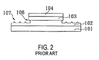
- an underlying protection film 102 of silicon oxide (SiO 2 ) is formed on a transparent insulating substrate 101 made of glass, and an amorphous silicon (a-Si) semiconductor film is formed on the underlying protection film 102 .
- excimer laser light is irradiated and scanned onto the semiconductor film to reform it polycrystalline.
- a polysilicon (p-Si) semiconductor film 103 is formed, on which a first gate oxide film 104 of silicon oxide is also formed.
- the polysilicon semiconductor film 103 and the first gate oxide film 104 are etched and pattered together into an island shape so as to form an island part 105 as shown in FIG. 1 B.
- selectivity of polysilicon and silicon oxide (defined by an etching speed of polysilicon/an etching speed of silicon oxide) is set to a comparatively high value.
- the reason why the high value is set as the selectivity is because, when the selectivity is comparatively low, the silicon oxide of the underlying protection film 102 is etched excessively and, as a result, the island part 105 has a wide step due to an undercut part 106 shown in FIG. 2 . Such a step results in disconnection of electrodes formed in the subsequent process or deterioration of yield due to a leak current flowing between the electrodes and the semiconductor film 103 . Furthermore, an undulation part 107 is formed on the surface of the underlying protection film 102 and lowers light transmittance of the transparent insulating substrate 101 . This brings about degradation of the quality of liquid crystal displays when such an undulated transparent insulating substrate 101 is used.
- a second gate oxide film 108 of silicon oxide is formed on the transparent insulating substrate 101 with the semiconductor film 103 and the first gate oxide film 104 .
- a conductive film composed of tantalum and the like is formed above the second gate oxide film 108 by spattering and the like, and is then patterned using photolithography technique to form a gate electrode 109 on the second gate oxide film 108 , as shown in FIG. 1 D.
- an impurity ion such as a phosphorus ion is implanted into the polysilicon semiconductor film 103 to form source/drain areas. Then, an interlayer insulating film 110 of silicon oxide is formed, as shown in FIG. 1 D.
- source/drain electrodes 111 are formed to be connected to the source/drain areas.
- the comparatively high selectivity of the polysilicon and silicon oxide in dry etching to form the island part 105 results in the formation of an overhang part 105 a shown in FIG. 1 B.
- an end portion or part of the first gate oxide film 104 projects outwardly from an end surface of the semiconductor film 103 .
- coverage becomes insufficient on the side walls of the island part 105 , as shown in FIG. 1 C.
- the Japanese Patent Laid-Open No. 2001-332741 proposes another technique in which, after the semiconductor film 103 and the first gate oxide film 104 are etched together into island shape, the first gate oxide film 104 is removed, and then the second gate oxide film 108 is formed.
- contamination is not avoidable on the surface of the semiconductor film 103 because the semiconductor film 103 is not covered until the second gate oxide film 108 is formed.
- a method of manufacturing a thin film transistor which includes a step of forming a first insulating film on a semiconductor film formed on a substrate; a step of forming an island by patterning the semiconductor film and the first insulating film into island shape; a step of forming a second insulating film on the island; and a step of forming a gate electrode on the second insulating film, characterized by comprising a step of removing an overhang part where a side end part of the first insulating film making the island is formed into visor shape over a side end part of the semiconductor film, the step of removing the overhang part being performed after the step of forming the island and before the step of forming the second insulating film.
- a method characterized in that in the step of removing the overhang part, the overhang part is removed by using a chemical cleaning liquid.
- a method of manufacturing the thin film transistor characterized in that in the step of removing the overhang part, the overhang part is removed by cleaning the substrate having the formed island for a time period from 1 to 60 seconds using an aqueous hydrofluoric acid solution of concentration ranging from 0.01% to 10% as the chemical cleaning liquid.
- a method of manufacturing the thin film transistor characterized in that in the step of removing the overhang part, of the first insulating film, there is left at least a region corresponding to a lower part of an area where the gate electrode is formed in the step of forming the gate electrode.
- a method of manufacturing a thin film transistor which include a step of forming a first insulating film on a semiconductor film formed on a substrate; a step of forming an island by patterning the semiconductor film and the first insulating film into island shape; a step of cleaning the substrate on which the island is formed; a step of forming a second insulating film on the island; and a step of forming a gate electrode on the second insulating film, characterized in that in the step of cleaning, an overhang part, where a side end part of the first insulating film making the island is formed into visor shape over a side end part of the semiconductor film, is removed simultaneously with cleaning processing.
- a method of manufacturing the thin film transistor characterized in that in the step of cleaning, the overhang part is removed by using a chemical cleaning liquid.
- a method of manufacturing the thin film transistor characterized in that in the step of cleaning, the overhang part is removed by cleaning the substrate having the formed island for a time period from 1 to 60 seconds using an aqueous hydrofluoric acid solution of concentration ranging from 0.01% to 10% as the chemical cleaning liquid.
- a method of manufacturing the thin film transistor characterized in that in the step of cleaning, of the first insulating film, there is left at least a region corresponding to a lower part of an area where the gate electrode is formed in the step of forming the gate electrode.
- the semiconductor film comprises a polycrystalline semiconductor.
- a method of manufacturing the thin film transistor characterized by comprising a semiconductor film forming step, which includes a non-single crystal semiconductor film forming step of forming a semiconductor film of a non-single crystal semiconductor on the substrate and an annealing step of crystallizing the semiconductor film of the non-single crystal semiconductor to form the semiconductor film of the polycrystalline semiconductor through annealing processing.
- the non-single crystal semiconductor includes an amorphous semiconductor.
- a method of manufacturing the thin film transistor characterized in that in the annealing step, the semiconductor film of the polycrystalline semiconductor is formed by irradiating the semiconductor film of the non-single crystal semiconductor with laser light.
- a method of manufacturing the thin film transistor characterized in that from start of the annealing step until end of the step of forming the first insulating film, predetermined processing is performed in a separated state from an outside air.
- FIGS. 1A to 1 E show sectional views for describing a conventional method.
- FIG. 2 shows an enlarged sectional view for describing the conventional method.
- FIGS. 3A to 3 G show process diagrams illustrating a method of manufacturing a TFT according to a first embodiment of the present invention
- FIGS. 4A to 4 E show process diagrams illustrating the method of manufacturing the TFT
- FIG. 5 is a schematic diagram showing a constitution of a TFT manufacturing apparatus which is used for manufacturing the TFT and which film deposition and laser irradiation to a transparent insulating substrate are performed in;
- FIG. 6 is a schematic diagram showing a constitution of a spin cleaning apparatus used for manufacturing the TFT
- FIGS. 7A to 7 F show process diagrams illustrating a method of manufacturing a TFT according to a second embodiment of the present invention
- a first insulating film is formed in a first insulating film forming process on a semiconductor film which is formed on a substrate, and then the semiconductor film and the first insulating film are patterned into island shape in an island forming process. Thereafter, an overhang part removal process or a cleaning process is carried out. In the overhang part removal process or the cleaning process, the overhang part, where a side end part of the first insulating film making the island is formed into a visor shape over a side end part of the semiconductor film, is removed. After this, a second insulating film is formed on the island in the second insulating film forming process, and a gate electrode is formed on the second insulating film in a gate electrode forming process.
- FIGS. 1 and 2 are process diagrams illustrating the method of manufacturing a TFT according to the first embodiment of the present invention
- FIG. 5 is a schematic diagram of a constitution of a TFT manufacturing apparatus which is used for manufacturing the TFT and in which film deposition and laser irradiation to the transparent insulating substrate are performed
- FIG. 6 is a schematic diagram of a constitution of a spin cleaning apparatus used for manufacturing the TFT.
- the transparent insulating substrate 1 is introduced into the TFT manufacturing apparatus 2 for manufacturing the TFT.
- the TFT manufacturing apparatus 2 is so constituted that a plurality of chambers are coupled with each other in which an object to be processed is subjected to respective predetermined processings, such chambers including a semiconductor film deposition part 2 a for forming a semiconductor film on the transparent insulating substrate 1 ; an insulator film deposition part 2 b for forming a silicon oxide film; a laser irradiation part 2 c for irradiating the object to be processed with a laser; and an introducing part 2 d for introducing the object to be processed such as the transparent insulating substrate 1 into a main unit of the TFT manufacturing apparatus from outside and removing it after the predetermined processings, all of which are disposed around a conveying part 2 f provided thereon with a conveying device 2 e.
- a semiconductor film deposition part 2 a for forming a semiconductor film on the transparent insulating substrate 1
- an insulator film deposition part 2 b for forming a silicon oxide film
- the conveying part 2 f and each of the semiconductor film deposition part 2 a, the insulator film deposition part 2 b, the laser irradiation part 2 c, and the introducing part 2 d is divided so as to be freely opened and closed by shutters 2 p, 2 q, 2 r, and 2 s, respectively, and the object to be processed is conveyed by the conveying device 2 e between the conveying part 2 f and each of the semiconductor film deposition part 2 a, the insulator film deposition part 2 b, the laser irradiation part 2 c, and the introducing part 2 d.
- the introducing part 2 d is provided with a delivery port for the object to be processed to/from the main unit of the TFT manufacturing apparatus, which is openable and closable by a shutter 2 t.
- PECVD Plasma Enhanced Chemical Vapor Deposition
- the underlying protection film 3 is provided in order to prevent separation caused from the diffusion of impurities such as a heavy metal from the transparent insulating substrate 1 .
- the film deposition is performed under the following condition: pressure (degree of vacuum) of 150 Pa, substrate temperature of 350° C., gas introduction of SiH 4 of 200 sccm (standard cubic centimeter per minute), which means 200 cc/min (200 cm 3 /min) at conversion in a standard state, N 2 O of 3000 sccm, and He of 100 sccm as material gases, and RF (Radio Frequency) power output of 1000 W.
- the transparent insulating substrate 1 on which the underlying protection film is formed, is transferred into the semiconductor film deposition part 2 a , and in succession to the film deposition of the underlying protection film 3 (FIG. 3 B), an amorphous silicon (a-Si) semiconductor film 4 with thickness of, for example, 500 ⁇ (50 nm), is formed on the underlying protection film 3 ( FIG. 3C ) by PECVD.
- a-Si amorphous silicon
- the film deposition is performed under the following condition: pressure of 50 Pa, substrate temperature of 400° C., gas introduction of SiH 4 of 140 sccm and Ar of 80 sccm as material gases, and RF power output of 120 W.
- the transparent insulating substrate 1 having the underlying protecting film 3 and the semiconductor film 4 undergoes a dehydrogenation treatment in which the transparent insulating substrate 1 is kept at 500° C. for 10 min.
- excimer laser light A is scan-irradiated on the amorphous silicon semiconductor film 4 in the laser irradiation part 2 c to make it polycrystalline, and then a polysilicon (p-Si) semiconductor film 5 is formed.
- an energy density is set to 400 mJ/cm 2
- a scan overlapping rate is set to 90% of beam width for example.
- the film deposition is performed under the following conditions: pressure of 110 Pa, substrate temperature of 380° C., gas introduction of TEOS of 180 sccm, O 2 of 3500 sccm, and He of 100 sccm as material gases, and RF power output of 1000 W.
- the transparent insulating substrate 1 having the semiconductor film 5 and the first gate oxide film 6 is removed from the TFT manufacturing apparatus 2 , and a resist mask with a predetermined mask pattern is formed on the surface of the first gate oxide mask 6 .
- a resist mask with a predetermined mask pattern is formed on the surface of the first gate oxide mask 6 .
- the polysilicon semiconductor film 5 and the first gate oxide film 6 are etched together by dry etching and pattered into island shape to form an island part 7 as shown in FIG. 3 F.
- the selectivity of the polysilicon and silicon oxide (etching speed of polysilicon/etching speed of silicon oxide) is changed in the middle of forming the island part 7 , which means that etching is performed in two stages of different etching conditions.
- the selectivity of etching the first gate oxide film 6 and etching the polysilicon semiconductor film 5 in a region within approximately 400 ⁇ (40 nm) in depth from its surface is set to, for example, 1, whereas the selectivity of etching the semiconductor film 5 in a region deeper than approximately 400 ⁇ (40 nm) from its surface is set to, for example, 20.
- the etching selectivity of a large portion etched from the start until the time immediately before the end of etching in the island forming process is set to an etching condition such that the silicon oxide and polysilicon are etched promptly and the formation of the overhang part in the foregoing description is suppressed.
- the selectivity of etching the remaining part until the end of etching after the selectivity is changed in the island forming process is set to an etching condition such that only the polysilicon is etched preventing the silicon oxide of the underlying protection film 3 from being etched and the generation of, for example, the undercut in the foregoing description, is avoided.
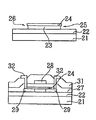
- an overhang part 8 of a visor shape is formed where the side end surface of the first gate oxide film 6 and that of the semiconductor film 5 are not aligned and the end part of the first gate oxide film 6 projects by approximately 2 ⁇ m from a position of the side end surface of the semiconductor film 5 .
- the overhang part 8 is removed simultaneously with cleaning in a cleaning/overhang part removal process which is subsequently performed.
- the spin cleaning apparatus 9 includes, as shown in FIG. 6 , a substrate chuck 9 a for vacuum-sucking a transparent insulating substrate 10 on which the island part 7 is formed; an AC servomotor 9 b for rotationally driving the substrate chuck 9 a around a rotational shaft; and a dispenser part 9 c for dropping a cleaning liquid.
- the spin cleaning apparatus 9 subjects the transparent insulating substrate 10 having the island part 7 to spin-cleaning using a hydrofluoric acid (HF) solution as the cleaning liquid to remove the overhang part 8 as well as dust.
- cleaning conditions including a concentration and drop time of the aqueous hydrofluoric acid solution, and the number of rotations (rotational speed) of the transparent insulating substrate 1 , are set optimally.
- the spin cleaning is performed dropping the aqueous hydrofluoric acid solution of concentration 1% for 30 sec. from above the transparent insulating substrate 1 having the semiconductor 5 and the first gate oxide film 6 , and rotating the transparent insulating substrate 1 at a rotational speed of 200 rpm.
- the concentration and drop time of the aqueous hydrofluoric acid solution, and the rotational speed of the transparent insulating substrate 1 when only the drop time is changed to 40 sec., the first gate oxide film 6 is completely removed. Also when only the concentration of the aqueous hydrofluoric acid solution is changed to 3%, the first gate oxide film 6 is completely removed.
- the aqueous hydrofluoric acid solution as the cleaning liquid is liable to stay on the transparent insulating substrate 1 , which increases the etching rate to the first gate oxide film 6 but causes a lowering of the removal effect of dust.
- the overhang part is removed and the end surface of the first gate oxide film 6 is retracted by approximately 3 ⁇ m from the side end surface of the semiconductor film 5 to the center thereof, as shown in FIG. 1 G.
- the first gate oxide film 6 is etched so that it may remain with predetermined thickness (approximately 30 ⁇ (3 nm) in this example), at least in a region directly under a gate electrode 12 which is formed in the subsequent process, that is, in a region directly above an area functioning as a channel of the semiconductor film 5 .
- a second gate oxide film (second insulating film) 11 with thickness of, for example, 600 ⁇ (60 nm), is formed on the transparent insulating substrate 1 having the semiconductor film 5 and the first gate oxide film 6 by PECVD. This allows the silicon oxide film to cover the side surface portion as well as the top surface portion of the polysilicon semiconductor film 5 , and an electrical insulating property is thereby maintained.
- a conductive film composed of tantalum and the like is formed from above the second gate oxide film 11 by spattering or the like, and is then patterned using photolithography technique to form the gate electrode 12 on the second gate oxide film 11 , as shown in FIG. 4 B.
- an impurity ion such as a phosphorus ion is implanted into the polysilicon semiconductor film 5 to form source/drain areas 13 , as shown in FIG. 4 C.
- an interlayer insulating film 14 of silicon oxide is formed by PECVD, as shown in FIG. 4 D.
- contact holes are formed, after which source/drain electrodes 15 are formed connected to the source/drain areas 13 (as in FIG. 4 E).
- the transparent insulating substrate 1 on which plural top gate TFTs 16 has been formed is thus obtained.
- These TFTs 16 are used, for example, as a switching element or part of a drive circuit in the active matrix of transmission type liquid crystal displays.
- the gate electrode 11 is connected to a scanning line, and the source/drain electrodes 15 are connected a signal line.
- Measurement of carrier mobility in the transparent insulating substrate 1 having the TFTs 16 provides an excellent result of 320 cm 2 /Vs on the average.
- calculation of standard deviationlaverage value for evaluation of less variations (uniformity) of the mobility in the transparent insulating substrate 1 provides a result of 5% or below.
- a yield of 99% or more is attained.
- the overhang part 8 formed in the island forming process can positively be removed by using the spin cleaning apparatus 9 in the cleaning/overhang part removal process, thus enhancing the yield.
- the semiconductor film 4 and the first gate oxide film 6 having a function of protecting the semiconductor film 4 are etched together to form the island part, and a clean interface between polysilicon and silicon oxide is formed, so that high carrier mobility and high uniformity thereof can be achieved.
- the transparent insulating substrate 1 is processed without being exposed to the outside air, so that the interface between the polysilicon and the silicon oxide can be maintained cleanly.
- the overhang part 8 is removed simultaneously with cleaning, which eliminates a special process as well as additional time for only removing the overhang part 8 . Therefore, the time necessary to manufacture TFTs can be reduced.
- FIG. 7 is a process diagram illustrating a method of manufacturing a TFT, which is a second embodiment of the present invention.
- the example here is considerably different from the first embodiment in that, in contrast that the film deposition and the laser irradiation to the transparent insulating substrate are performed in the TFT manufacturing apparatus without exposing the transparent insulating substrate to the outside air, such film deposition and laser irradiation are performed in different apparatus, and that the transparent insulating substrate having the island part is only immersed in the aqueous hydrofluoric acid solution in substitution for the spin-cleaning in the cleaning/overhang part removal process.
- the film deposition of the underlying protection film and the semiconductor film onto the transparent insulating substrate are performed by a Low Pressure Chemical Vapor Deposition (hereinafter referred to as LPCVD) apparatus employing LPCVD technique, and the film deposition of the first gate oxide film onto the transparent insulating substrate having the island part is performed by a PECVD apparatus employing PECVD technique.
- LPCVD Low Pressure Chemical Vapor Deposition
- PECVD apparatus employing PECVD technique
- the laser irradiation to the amorphous silicon semiconductor film to form the polysilicon semiconductor film is performed by a dedicated laser irradiation apparatus.
- a transparent insulating substrate 21 made of glass which is cleaned by ultrasonic cleaning and the like (e.g., No. 1737 of Corning Incorporated, or the like) is prepared, as shown in FIG. 7 A.
- an amorphous silicon semiconductor film with thickness of, for example, 500 ⁇ (50 nm), is formed on the underlying protection film 22 by LPCVD.
- the film deposition is performed under the following conditions: pressure of 10 Pa, substrate temperature 450° C., and gas introduction of Si 2 H 6 of 200 sccm as a material gas.
- excimer laser light is scan-irradiated on the amorphous silicon semiconductor film to make it crystalline, and thus a polysilicon semiconductor film 23 is formed.
- the energy density of the excimer laser light is set to 410 mJ/cm 2
- the scan overlapping rate is set to 90% of beam width, for example.
- the transparent insulating substrate 21 having the semiconductor film 23 is removed from the laser irradiation apparatus and is then subjected to RCA cleaning processing and HF cleaning processing. More specifically, by using, as a cleaning liquid, a mixed solution of NH 4 OH solution, H 2 O 2 solution, and H 2 O in a predetermined mixture ratio, or a mixed solution of HCl solution, H 2 O 2 solution, and H 2 O in a predetermined mixture ratio, the transparent insulating substrate 21 is cleaned at 75° C. to 85° C. for 10 to 20 min., and is thereafter cleaned by the hydrofluoric acid (HF) solution as the cleaning liquid.
- a cleaning liquid a mixed solution of NH 4 OH solution, H 2 O 2 solution, and H 2 O in a predetermined mixture ratio
- a mixed solution of HCl solution, H 2 O 2 solution, and H 2 O in a predetermined mixture ratio
- a resist mask with a predetermined mask pattern is formed on the surface of the first gate oxide film 24 , and using photolithography technique, the polysilicon semiconductor film 23 and the first gate oxide film 24 are etched and patterned together into island shape to form an island 25 , as shown in FIG. 7 B.
- the selectivity of polysilicon and silicon oxide (etching speed of polysilicon/etching speed of silicon oxide) is changed in the middle of forming the island 25 , which means that etching is performed in two stages of different etching conditions.
- the selectivity of etching the first gate oxide film 24 and etching the polysilicon semiconductor film 23 in a region within approximately 400 ⁇ (40 nm) in depth from its surface is set to, for example, 1, whereas the selectivity of etching the semiconductor film 23 in a region deeper than approximately 400 ⁇ (40 nm) from its surface is set to, for example, 20.
- an overhang part 26 is formed where the side end surface of the first gate oxide film 24 and that of the semiconductor film 23 are not aligned and the end part of the first gate oxide film 24 projects by approximately 1 ⁇ m from a position of the side end surface of the semiconductor film 23 .
- the transparent insulating substrate 21 having the island 25 undergoes the RCA cleaning processing, and is then immersed in the aqueous hydrofluoric acid solution of concentration 0.5% for 10 sec. for cleaning to remove the overhang part 26 as well as dust.
- the first gate oxide film 24 is etched so that it may remain with predetermined thickness (approximately 50 ⁇ (5 nm) in this example), at least in a region directly under a gate electrode 28 which is formed in the subsequent process, that is, in a region directly above an area functioning as a channel of the semiconductor film 23 .
- a second gate oxide film 27 is formed on the transparent insulating substrate 21 having the semiconductor film 23 and the first gate oxide film 24 by PECVD.
- a conductive film composed of tantalum and the like is formed from above the second gate oxide film 27 by spattering or the like, and is then patterned using photolithography technique to form the gate electrode 28 on the second gate oxide film 27 as shown in FIG. 7 E.
- an impurity ion such as a phosphorus ion is implanted into the polysilicon semiconductor film 23 to form source/drain areas 29 as shown in FIG. 2 E.
- an interlayer insulating film 31 of silicon oxide is formed by PECVD.
- contact holes are formed, after which source/drain electrodes 32 are formed connected to the source/drain areas 29 .
- Measurement of carrier mobility in the transparent insulating substrate 21 having the above TFT provides an excellent result of 290 cm 2 /Vs on the average.
- calculation of standard deviation/average value for evaluation of less variations (uniformity) of the carrier mobility in the transparent insulating substrate 21 provides a result of 5% or below.
- a yield of 99% or more is attained.
- the TFT in the present invention is used as a switching element and the like of liquid crystal displays, however, it is not limited to liquid crystal displays, and the TFT may alternatively be applied to organic EL displays and the like.
- cleaning conditions are not restricted to those and may appropriately be changeable, for example, it may alternatively be possible that the aqueous hydrofluoric acid solution of concentration 0.01% is dropped for 60 sec., or also that the aqueous hydrofluoric acid solution of concentration 10% is dropped for 1 second. Under such conditions, the overhang part 8 can be removed, thus enhancing the yield.
- the number of rotations is not limited to 200 rpm and may be changeable, for example, within several 10%, without changing the concentration and drop time of the aqueous hydrofluoric acid solution, or may alternatively be changed in combination with the concentration or drop time.
- cleaning conditions are set depending on the thickness and the like of the first gate oxide film 6 .
- aqueous hydrofluoric acid solution is used as a cleaning liquid, however, it may alternatively be possible that an aqueous buffered hydrofluoric acid solution including NH 4 F as a buffer solution is used, for example.
- the etching condition and film deposition condition are also not limited to those described above, and the selectivity of etching the first gate oxide film 6 and etching the polysilicon semiconductor film 5 in the region within approximately 400 ⁇ (40 nm) in depth from its surface, and the selectivity of etching the semiconductor film 5 in the region deeper than approximately 400 ⁇ (40 nm) from its surface, are not limited to 1, 20, respectively, and those may appropriately be changeable.
- the etching condition and film deposition condition are set depending on the thickness and the like of the first gate oxide film 6 and the semiconductor film 5 .
- the transparent insulating substrate 1 is immersed in the aqueous hydrofluoric acid solution of concentration 0.5% for 10 sec.
- the concentration of and immersion time in the aqueous hydrofluoric acid solution may appropriately be changeable and are set optimally depending on the thickness and the like of the first gate oxide film 6 .
- the transparent insulating substrate 1 is immersed in the aqueous hydrofluoric acid solution of concentration 0.01% for 60 sec., or immersed in the aqueous hydrofluoric acid solution of concentration 10% for 1 second.
- first and second gate insulating films may alternatively be possible to form the first and second gate insulating films by, for example, depositing silicon nitride instead of silicon oxide.
- the gate electrode may be formed by the use of metals, such as aluminum, chromium, molybdenum, or the like, instead of tantalum.
- the semiconductor film may be formed by amorphous silicon instead of polysilicon, and in this case the overhang part can be positively removed.
- the overhang part formed in the island forming process can be positively removed, thus enhancing the yield.
- a clean interface between polysilicon and silicon oxide can be formed, so that high carrier mobility and high uniformity thereof can be achieved.
- processing is performed in a separated state from the outside air, so that the interface between the polycrystalline semiconductor film and the oxide silicon film can particularly be maintained cleanly.
- the overhang part is removed simultaneously with cleaning in the cleaning process, which eliminates a special process as well as additional time for only removing the overhang part. Therefore, the time necessary to manufacture TFTs can be reduced.
Abstract
Description
Claims (18)
Applications Claiming Priority (2)
| Application Number | Priority Date | Filing Date | Title |
|---|---|---|---|
| JPJP2002-146918 | 2002-05-21 | ||
| JP2002146918A JP4243455B2 (en) | 2002-05-21 | 2002-05-21 | Thin film transistor manufacturing method |
Publications (2)
| Publication Number | Publication Date |
|---|---|
| US20040005743A1 US20040005743A1 (en) | 2004-01-08 |
| US7011996B2 true US7011996B2 (en) | 2006-03-14 |
Family
ID=29705749
Family Applications (1)
| Application Number | Title | Priority Date | Filing Date |
|---|---|---|---|
| US10/444,288 Expired - Fee Related US7011996B2 (en) | 2002-05-21 | 2003-05-22 | Method of manufacturing thin film transistor |
Country Status (5)
| Country | Link |
|---|---|
| US (1) | US7011996B2 (en) |
| JP (1) | JP4243455B2 (en) |
| KR (1) | KR100552219B1 (en) |
| CN (1) | CN1212654C (en) |
| TW (1) | TWI239104B (en) |
Cited By (5)
| Publication number | Priority date | Publication date | Assignee | Title |
|---|---|---|---|---|
| US20050285112A1 (en) * | 2004-06-29 | 2005-12-29 | Eui-Hoon Hwang | Thin film transistor and method for fabricating the same |
| US20060088962A1 (en) * | 2004-10-22 | 2006-04-27 | Herman Gregory S | Method of forming a solution processed transistor having a multilayer dielectric |
| US20060094168A1 (en) * | 2004-10-29 | 2006-05-04 | Randy Hoffman | Method of forming a thin film component |
| US20090032890A1 (en) * | 2007-07-30 | 2009-02-05 | Hewlett-Packard Development | Multilayer dielectric |
| US20120326157A1 (en) * | 2011-06-21 | 2012-12-27 | Samsung Mobile Display Co., Ltd. | Method of Manufacturing Thin Film Transistor, Thin Film Transistor Manufactured Using the Method, Method of Manufacturing Organic Light-Emitting Display Apparatus, and Organic Light-Emitting Display Apparatus Manufactured Using the Method |
Families Citing this family (7)
| Publication number | Priority date | Publication date | Assignee | Title |
|---|---|---|---|---|
| KR100611886B1 (en) * | 2004-06-25 | 2006-08-11 | 삼성에스디아이 주식회사 | Pixel circuit and organic light emitting display having an improved transistor structure |
| US7135346B2 (en) * | 2004-07-29 | 2006-11-14 | International Business Machines Corporation | Structure for monitoring semiconductor polysilicon gate profile |
| JP4513564B2 (en) * | 2004-12-28 | 2010-07-28 | 富士電機システムズ株式会社 | Semiconductor device manufacturing method and semiconductor device manufacturing apparatus |
| JP5499525B2 (en) * | 2009-06-15 | 2014-05-21 | 大日本印刷株式会社 | Semiconductor device manufacturing method and display device |
| TWI419336B (en) * | 2011-08-26 | 2013-12-11 | Au Optronics Corp | Semiconductor device and method of making the same |
| KR102492394B1 (en) * | 2017-04-28 | 2023-01-27 | 도쿄엘렉트론가부시키가이샤 | Application processing device, application processing method, and optical film forming device |
| JP7398969B2 (en) | 2019-03-01 | 2023-12-15 | 東京エレクトロン株式会社 | Substrate processing method, substrate processing apparatus and storage medium |
Citations (12)
| Publication number | Priority date | Publication date | Assignee | Title |
|---|---|---|---|---|
| US4704784A (en) * | 1984-06-22 | 1987-11-10 | Thomson-Csf | Method of making thin film field effect transistors for a liquid crystal display device |
| US5039621A (en) * | 1990-06-08 | 1991-08-13 | Texas Instruments Incorporated | Semiconductor over insulator mesa and method of forming the same |
| US5120667A (en) * | 1990-05-17 | 1992-06-09 | Sharp Kabushiki Kaisha | Process for fabricating a thin film transistor |
| US5328861A (en) * | 1991-11-25 | 1994-07-12 | Casio Computer Co., Ltd. | Method for forming thin film transistor |
| US5470762A (en) * | 1991-11-29 | 1995-11-28 | Semiconductor Energy Laboratory Co., Ltd. | Method of fabricating a thin film transistor |
| US5624861A (en) * | 1995-08-28 | 1997-04-29 | Sharp Kabushiki Kaisha | Method of manufacturing semiconductor device |
| US5998838A (en) * | 1997-03-03 | 1999-12-07 | Nec Corporation | Thin film transistor |
| KR20000018289A (en) | 1998-09-01 | 2000-04-06 | 구본준, 론 위라하디락사 | Thin film transistor and manufacturing method thereof |
| US6403409B1 (en) * | 1999-08-30 | 2002-06-11 | Samsung Electronics Co., Ltd. | Method for fabricating top gate type polycrystalline silicon thin film transistor |
| US6444507B1 (en) * | 1996-10-22 | 2002-09-03 | Seiko Epson Corporation | Fabrication process for thin film transistors in a display or electronic device |
| US20020192885A1 (en) * | 1998-05-14 | 2002-12-19 | Seiko Epson Corporation | Fabrication process for thin film transistors in a display or electronic device |
| US6737302B2 (en) * | 2001-10-31 | 2004-05-18 | Semiconductor Energy Laboratory Co., Ltd. | Manufacturing method for field-effect transistor |
-
2002
- 2002-05-21 JP JP2002146918A patent/JP4243455B2/en not_active Expired - Fee Related
-
2003
- 2003-05-20 KR KR1020030031832A patent/KR100552219B1/en not_active IP Right Cessation
- 2003-05-21 CN CNB031378196A patent/CN1212654C/en not_active Expired - Fee Related
- 2003-05-21 TW TW092113703A patent/TWI239104B/en not_active IP Right Cessation
- 2003-05-22 US US10/444,288 patent/US7011996B2/en not_active Expired - Fee Related
Patent Citations (15)
| Publication number | Priority date | Publication date | Assignee | Title |
|---|---|---|---|---|
| US4704784A (en) * | 1984-06-22 | 1987-11-10 | Thomson-Csf | Method of making thin film field effect transistors for a liquid crystal display device |
| US5120667A (en) * | 1990-05-17 | 1992-06-09 | Sharp Kabushiki Kaisha | Process for fabricating a thin film transistor |
| US5039621A (en) * | 1990-06-08 | 1991-08-13 | Texas Instruments Incorporated | Semiconductor over insulator mesa and method of forming the same |
| US5328861A (en) * | 1991-11-25 | 1994-07-12 | Casio Computer Co., Ltd. | Method for forming thin film transistor |
| US5470762A (en) * | 1991-11-29 | 1995-11-28 | Semiconductor Energy Laboratory Co., Ltd. | Method of fabricating a thin film transistor |
| US5624861A (en) * | 1995-08-28 | 1997-04-29 | Sharp Kabushiki Kaisha | Method of manufacturing semiconductor device |
| US6444507B1 (en) * | 1996-10-22 | 2002-09-03 | Seiko Epson Corporation | Fabrication process for thin film transistors in a display or electronic device |
| US5998838A (en) * | 1997-03-03 | 1999-12-07 | Nec Corporation | Thin film transistor |
| US6258638B1 (en) * | 1997-03-03 | 2001-07-10 | Nec Corporation | Method of manufacturing thin film transistor |
| US6444508B1 (en) * | 1997-03-03 | 2002-09-03 | Nec Corporation | Method of manufacturing thin film transistor |
| US6703267B2 (en) * | 1997-03-03 | 2004-03-09 | Nec Corporation | Method of manufacturing thin film transistor |
| US20020192885A1 (en) * | 1998-05-14 | 2002-12-19 | Seiko Epson Corporation | Fabrication process for thin film transistors in a display or electronic device |
| KR20000018289A (en) | 1998-09-01 | 2000-04-06 | 구본준, 론 위라하디락사 | Thin film transistor and manufacturing method thereof |
| US6403409B1 (en) * | 1999-08-30 | 2002-06-11 | Samsung Electronics Co., Ltd. | Method for fabricating top gate type polycrystalline silicon thin film transistor |
| US6737302B2 (en) * | 2001-10-31 | 2004-05-18 | Semiconductor Energy Laboratory Co., Ltd. | Manufacturing method for field-effect transistor |
Non-Patent Citations (3)
| Title |
|---|
| English translation of relevant portions of Korean Patent Office Action issued May 16, 2005 submitted in lieu of statement of relevancy of prior art teachings to the instant application. |
| Japanese translation of Korean Office action prepared by Korean associate and sent to Japanese associate. |
| Untranslated Korean Office Action issued on May 16, 2005 in connection with corresponding Korean application No. 10-2003-0031832. |
Cited By (12)
| Publication number | Priority date | Publication date | Assignee | Title |
|---|---|---|---|---|
| US20050285112A1 (en) * | 2004-06-29 | 2005-12-29 | Eui-Hoon Hwang | Thin film transistor and method for fabricating the same |
| US20060088962A1 (en) * | 2004-10-22 | 2006-04-27 | Herman Gregory S | Method of forming a solution processed transistor having a multilayer dielectric |
| US20060094168A1 (en) * | 2004-10-29 | 2006-05-04 | Randy Hoffman | Method of forming a thin film component |
| US7374984B2 (en) * | 2004-10-29 | 2008-05-20 | Randy Hoffman | Method of forming a thin film component |
| US20080197414A1 (en) * | 2004-10-29 | 2008-08-21 | Randy Hoffman | Method of forming a thin film component |
| US7799624B2 (en) * | 2004-10-29 | 2010-09-21 | Hewlett-Packard Development Company, L.P. | Method of forming a thin film component |
| US20090032890A1 (en) * | 2007-07-30 | 2009-02-05 | Hewlett-Packard Development | Multilayer dielectric |
| US7768080B2 (en) | 2007-07-30 | 2010-08-03 | Hewlett-Packard Development Company, L.P. | Multilayer dielectric |
| US20100279514A1 (en) * | 2007-07-30 | 2010-11-04 | Hewlett-Packard Development Company Lp | Multilayer dielectric |
| US8143128B2 (en) | 2007-07-30 | 2012-03-27 | Hewlett-Packard Development Company, L.P. | Multilayer dielectric defect method |
| US20120326157A1 (en) * | 2011-06-21 | 2012-12-27 | Samsung Mobile Display Co., Ltd. | Method of Manufacturing Thin Film Transistor, Thin Film Transistor Manufactured Using the Method, Method of Manufacturing Organic Light-Emitting Display Apparatus, and Organic Light-Emitting Display Apparatus Manufactured Using the Method |
| US8815663B2 (en) * | 2011-06-21 | 2014-08-26 | Samsung Display Co., Ltd. | Method of manufacturing thin film transistor, thin film transistor manufactured using the method, method of manufacturing organic light-emitting display apparatus, and organic light-emitting display apparatus manufactured using the method |
Also Published As
| Publication number | Publication date |
|---|---|
| US20040005743A1 (en) | 2004-01-08 |
| JP2003338506A (en) | 2003-11-28 |
| TW200408135A (en) | 2004-05-16 |
| KR20030091690A (en) | 2003-12-03 |
| CN1461048A (en) | 2003-12-10 |
| JP4243455B2 (en) | 2009-03-25 |
| TWI239104B (en) | 2005-09-01 |
| KR100552219B1 (en) | 2006-02-14 |
| CN1212654C (en) | 2005-07-27 |
Similar Documents
| Publication | Publication Date | Title |
|---|---|---|
| US7442592B2 (en) | Manufacturing a semiconductor device | |
| JP3409542B2 (en) | Method for manufacturing semiconductor device | |
| EP1102111B1 (en) | Liquid crystal display device having improved TFTs and a fabrication method thereof | |
| JP4082459B2 (en) | Manufacturing method of display device | |
| KR20020092255A (en) | Semiconductor film, semiconductor device and method of their production | |
| JPH11204435A (en) | Semiconductor device and preparation of the same | |
| US7011996B2 (en) | Method of manufacturing thin film transistor | |
| US6033973A (en) | Ion doping device and method of cleaning ion doping system | |
| US20060051905A1 (en) | Method of fabricating planarized poly-silicon thin film transistors | |
| WO2001061760A1 (en) | Method of manufacturing thin-film transistor, and liquid-crystal display | |
| JP2776276B2 (en) | Method for manufacturing thin film transistor | |
| JP2001189462A (en) | Manufacturing method of semiconductor device | |
| US6482685B1 (en) | Method for fabricating a low temperature polysilicon thin film transistor incorporating multi-layer channel passivation step | |
| JP3358284B2 (en) | Method for manufacturing thin film transistor | |
| JP3279280B2 (en) | Method for manufacturing thin film semiconductor device | |
| KR100752370B1 (en) | Thin Film transistor and method for fabricating the same | |
| JP2002190606A (en) | Method for manufacturing top gate thin-film transistor | |
| JP2877129B2 (en) | Thin film transistor and method of manufacturing the same | |
| JP2004165286A (en) | Method for manufacturing thin film transistor | |
| JP3602344B2 (en) | Thin film transistor and method for manufacturing the same | |
| JP2007165774A (en) | Thin-film laminated substrate, manufacturing method therefor and display device | |
| JP2004125881A (en) | Method for washing substrate | |
| JPH09116164A (en) | Normal stagger type film transistor, and its manufacture | |
| JP2004071979A (en) | Active matrix display device and method for manufacturing the same | |
| JP2005057045A (en) | Method of manufacturing thin film transistor, thin film transistor, and liquid crystal display device |
Legal Events
| Date | Code | Title | Description |
|---|---|---|---|
| AS | Assignment |
Owner name: NEC LCD TECHNOLOGIES, LTD., JAPAN Free format text: ASSIGNMENT OF ASSIGNORS INTEREST;ASSIGNORS:OKUMURA, HIROSHI;SHIOTA, KUNIHIRO;REEL/FRAME:014112/0538 Effective date: 20030519 Owner name: NEC CORPORATION, JAPAN Free format text: ASSIGNMENT OF ASSIGNORS INTEREST;ASSIGNORS:OKUMURA, HIROSHI;SHIOTA, KUNIHIRO;REEL/FRAME:014112/0538 Effective date: 20030519 |
|
| FEPP | Fee payment procedure |
Free format text: PAYOR NUMBER ASSIGNED (ORIGINAL EVENT CODE: ASPN); ENTITY STATUS OF PATENT OWNER: LARGE ENTITY |
|
| FPAY | Fee payment |
Year of fee payment: 4 |
|
| AS | Assignment |
Owner name: NEC CORPORATION,JAPAN Free format text: ASSIGNMENT OF ASSIGNORS INTEREST;ASSIGNOR:NEC LCD TECHNOLOGIES, LTD.;REEL/FRAME:024494/0980 Effective date: 20100301 Owner name: NEC CORPORATION, JAPAN Free format text: ASSIGNMENT OF ASSIGNORS INTEREST;ASSIGNOR:NEC LCD TECHNOLOGIES, LTD.;REEL/FRAME:024494/0980 Effective date: 20100301 |
|
| FEPP | Fee payment procedure |
Free format text: PAYER NUMBER DE-ASSIGNED (ORIGINAL EVENT CODE: RMPN); ENTITY STATUS OF PATENT OWNER: LARGE ENTITY Free format text: PAYOR NUMBER ASSIGNED (ORIGINAL EVENT CODE: ASPN); ENTITY STATUS OF PATENT OWNER: LARGE ENTITY |
|
| AS | Assignment |
Owner name: GETNER FOUNDATION LLC, DELAWARE Free format text: ASSIGNMENT OF ASSIGNORS INTEREST;ASSIGNOR:NEC CORPORATION;REEL/FRAME:026254/0381 Effective date: 20110418 |
|
| REMI | Maintenance fee reminder mailed | ||
| LAPS | Lapse for failure to pay maintenance fees | ||
| STCH | Information on status: patent discontinuation |
Free format text: PATENT EXPIRED DUE TO NONPAYMENT OF MAINTENANCE FEES UNDER 37 CFR 1.362 |
|
| FP | Lapsed due to failure to pay maintenance fee |
Effective date: 20140314 |
|
| AS | Assignment |
Owner name: VISTA PEAK VENTURES, LLC, TEXAS Free format text: ASSIGNMENT OF ASSIGNORS INTEREST;ASSIGNOR:GETNER FOUNDATION LLC;REEL/FRAME:045469/0164 Effective date: 20180213 |