JP4255534B2 - Game machine - Google Patents
Game machine Download PDFInfo
- Publication number
- JP4255534B2 JP4255534B2 JP19655198A JP19655198A JP4255534B2 JP 4255534 B2 JP4255534 B2 JP 4255534B2 JP 19655198 A JP19655198 A JP 19655198A JP 19655198 A JP19655198 A JP 19655198A JP 4255534 B2 JP4255534 B2 JP 4255534B2
- Authority
- JP
- Japan
- Prior art keywords
- control board
- board
- game
- ball
- power supply
- Prior art date
- Legal status (The legal status is an assumption and is not a legal conclusion. Google has not performed a legal analysis and makes no representation as to the accuracy of the status listed.)
- Expired - Lifetime
Links
Images


Description
【0001】
【発明の属する技術分野】
本発明は、遊技者の操作に応じて遊技が行われるパチンコ遊技機やコイン遊技機等の遊技機に関し、特に、遊技盤における遊技領域において遊技者の操作に応じて遊技が行われる遊技機に関する。
【0002】
【従来の技術】
遊技機として、表示状態が変化可能な可変表示部を有する可変表示装置が設けられ、可変表示部の表示結果があらかじめ定められた特定の表示態様となった場合に遊技者に有利となる特定遊技状態に移行するように構成されたものがある。可変表示装置には複数の可変表示部があり、通常、複数の可変表示部の表示結果を時期を異ならせて表示するように構成されている。可変表示部には、例えば、図柄等の複数の識別情報が可変表示される。可変表示部の表示結果があらかじめ定められた特定の表示態様の組合せとなることを、通常、「大当り」という。なお、遊技価値とは、遊技機の遊技領域に設けられた可変入賞球装置の状態が打球が入賞しやすい遊技者にとって有利な状態になることや、遊技者にとって有利な状態となるための権利を発生させたりすることである。
【0003】
大当りが発生すると、例えば、大入賞口が所定回数開放して打球が入賞しやすい大当り遊技状態に移行する。そして、各開放期間において、所定個(例えば10個)の大入賞口への入賞があると大入賞口は閉成する。そして、大入賞口の開放回数は、所定回数(例えば15ラウンド)に固定されている。なお、各開放について開放時間(例えば29.5秒)が決められ、入賞数が所定個に達しなくても開放時間が経過すると大入賞口は閉成する。また、大入賞口が閉成した時点で所定の条件(例えば、大入賞口内に設けられているVゾーンへの入賞)が成立していない場合には、大当り遊技状態は終了する。
【0004】
大当りの発生等を含む遊技の進行は、遊技盤の裏面に設置される遊技制御基板(主制御基板)に搭載される遊技制御用のマイクロコンピュータ回路によって制御される。また、遊技盤面や枠内部には、遊技効果を増進するためのランプ,LEDやスピーカ等が設置されている。それらのオン/オフ制御を行うための回路を搭載した基板も遊技盤の裏面に設置されている。また、大当りを生じさせるための可変表示部の表示を制御する各回路を搭載した表示制御基板、打球の発射制御を行う各回路を搭載した発射制御基板、賞球や貸玉の払出制御を行う賞球基板等も遊技盤の裏面に設置されている。
【0005】
スピーカは、主制御基板に搭載される遊技制御用のマイクロコンピュータ回路によって制御されるが、マイクロコンピュータ回路の動作電圧である5Vとは異なる電圧で駆動される。よって、必要な電流増幅が主制御基板において行われる。スピーカは、一般に、遊技機における枠側に設置される。遊技効果を増進するためのランプおよびLEDも、一般に、遊技機における枠側に設置される。従って、ランプ、LEDおよびスピーカへの信号線は、1つの電飾基板(一般に、ランプおよびLEDを増幅する回路が搭載される)を介して枠側に配線される。また、遊技機の設置状況に合わせてスピーカらの音量を調整するために音量調整スイッチが設けられているが、音量調整スイッチは音声信号の通り道となる電飾基板に設置される。
【0006】
【発明が解決しようとする課題】
従来の遊技機は以上のように構成されているので、機種変更の際に音声制御に変更があると、主制御基板を作り替えなければならなくなる場合が生ずる。また、音量調整スイッチの設置位置や種類が変更される場合に、ランプおよびLEDに変更がなくても、電飾基板を作り替えなければならなくなる場合が生ずる。すなわち、従来の遊技機では、音声制御に関わる変更が主制御基板等の作り替えを引き起こす可能性がある。その結果、遊技機の製造コストを下げることにも限界が生ずる。
【0007】
本発明は、そのような課題を解決するためになされたものであって、製造コストを下げることができるとともに基板の長寿命化を図ることができる遊技機を提供することを目的とする。
【0008】
【課題を解決するための手段】
本発明による遊技機は、遊技盤に遊技領域が設けられ、遊技者の操作に応じて遊技が行われ、遊技進行を制御する遊技制御手段が搭載された遊技制御基板と、遊技制御基板からの信号にもとづいて遊技盤に設けられている可変表示部の表示制御を行う表示制御手段が搭載された表示制御基板とを含む遊技機であって、少なくとも遊技制御基板および表示制御基板とは別に設けられた基板であって遊技制御基板からの情報にもとづいて音声に関する制御を行う音声制御基板と、遊技制御基板および音声制御基板を含む各基板に電源を供給する電源基板とを備え、音声制御基板は、音量切替手段を搭載し、電源基板は、各基板に搭載されているICを駆動するための駆動電源より電圧の高い供給電源を作成して各基板に供給し、各基板は、駆動電源を電源基板から該各基板に供給される供給電源から生成する駆動電源生成手段をそれぞれ搭載していることを特徴とする。
【0009】
ここで、音量切替手段は、音声制御基板に搭載されている音量増幅手段よりも前段に配置されていてもよい。
また、音声制御基板に搭載される音声データを記憶している音声データ記憶手段は、音声制御基板に着脱可能に搭載されていてもよい。
【0010】
【発明の実施の形態】
以下、本発明の一実施形態を図面を参照して説明する。
まず、遊技機の一例であるパチンコ遊技機の全体の構成について説明する。図1はパチンコ遊技機1を正面からみた正面図である。なお、ここでは、遊技機の一例としてパチンコ遊技機を示すが、本発明はパチンコ遊技機に限られず、例えばコイン遊技機等であってもよい。
【0011】
図1に示すように、パチンコ遊技機1は、額縁状に形成されたガラス扉枠2を有する。ガラス扉枠2の下部表面には打球供給皿3がある。打球供給皿3の下部には、打球供給皿3からあふれた景品玉を貯留する余剰玉受皿4と打球を発射する打球操作ハンドル(操作ノブ)5が設けられている。ガラス扉枠2の後方には、遊技盤6が着脱可能に取り付けられている。また、遊技盤6の前面には遊技領域7が設けられている。
【0012】
遊技領域7の中央付近には、複数種類の図柄を可変表示するための可変表示部9と7セグメントLEDによる可変表示器10とを含む可変表示装置8が設けられている。可変表示部9には、「左」、「中」、「右」の3つの図柄表示エリアがある。可変表示装置8の側部には、打球を導く通過ゲート11が設けられている。通過ゲート11を通過した打球は、玉出口13を経て始動入賞口14の方に導かれる。通過ゲート11と玉出口13との間の通路には、通過ゲート11を通過した打球を検出するゲートスイッチ12がある。また、始動入賞口14に入った入賞球は、遊技盤6の背面に導かれ、始動口スイッチ17によって検出される。また、始動入賞口14の下部には開閉動作を行う可変入賞球装置15が設けられている。可変入賞球装置15は、ソレノイド16によって開状態とされる。
【0013】
可変入賞球装置15の下部には、特定遊技状態(大当り状態)においてソレノイド21によって開状態とされる開閉板20が設けられている。この実施の形態では、開閉板20が大入賞口を開閉する手段となる。開閉板20から遊技盤6の背面に導かれた入賞球のうち一方(Vゾーン)に入った入賞球はVカウントスイッチ22で検出される。また、開閉板20からの入賞球はカウントスイッチ23で検出される。可変表示装置8の下部には、始動入賞口14に入った入賞球数を表示する4個の表示部を有する始動入賞記憶表示器18が設けられている。この例では、4個を上限として、始動入賞がある毎に、始動入賞記憶表示器18は点灯している表示部を1つずつ増やす。そして、可変表示部9の可変表示が開始される毎に、点灯している表示部を1つ減らす。
【0014】
遊技盤6には、複数の入賞口19,24が設けられている。遊技領域7の左右周辺には、遊技中に点滅表示される装飾ランプ25が設けられ、下部には、入賞しなかった打球を吸収するアウト口26がある。また、遊技領域7の外側の左右上部には、効果音を発する2つのスピーカ27が設けられている。遊技領域7の外周には、遊技効果LED28aおよび遊技効果ランプ28b,28cが設けられている。そして、この例では、一方のスピーカ27の近傍に、景品玉払出時に点灯する賞球ランプ51が設けられ、他方のスピーカ27の近傍に、補給玉が切れたときに点灯する玉切れランプ52が設けられている。さらに、図1には、パチンコ遊技台1に隣接して設置され、プリペイドカードが挿入されることによって玉貸しを可能にするカードユニット50も示されている。
【0015】
打球発射装置から発射された打球は、打球レールを通って遊技領域7に入り、その後、遊技領域7を下りてくる。打球が通過ゲート11を通ってゲートスイッチ12で検出されると、可変表示器10の表示数字が連続的に変化する状態になる。また、打球が始動入賞口14に入り始動口スイッチ17で検出されると、図柄の変動を開始できる状態であれば、可変表示部9内の図柄が回転を始める。図柄の変動を開始できる状態でなければ、始動入賞記憶を1増やす。なお、始動入賞記憶については、後で詳しく説明する。可変表示部9内の画像の回転は、一定時間が経過したときに停止する。停止時の画像の組み合わせが大当り図柄の組み合わせであると、大当り遊技状態に移行する。すなわち、開閉板20が、一定時間経過するまで、または、所定個数(例えば10個)の打球が入賞するまで開放する。そして、開閉板20の開放中に打球が特定入賞領域に入賞しVカウントスイッチ22で検出されると、継続権が発生し開閉板20の開放が再度行われる。この継続権の発生は、所定回数(例えば15ラウンド)許容される。
【0016】
停止時の可変表示部9内の画像の組み合わせが確率変動を伴う大当り図柄の組み合わせである場合には、次に大当りとなる確率が高くなる。すなわち、高確率状態という遊技者にとってさらに有利な状態となる。
また、可変表示器10における停止図柄が所定の図柄(当り図柄)である場合に、可変入賞球装置15が所定時間だけ開状態になる。さらに、高確率状態では、可変表示器10における停止図柄が当り図柄になる確率が高められるとともに、可変入賞球装置15の開放時間と開放回数が高められる。
【0017】
次に、パチンコ遊技機1の裏面に配置されている各基板について説明する。
図2に示すように、パチンコ遊技機1の裏面では、枠体2A内の機構板の上部に玉貯留タンク38が設けられ、パチンコ遊技機1が遊技機設置島に設置された状態でその上方から遊技球が玉貯留タンク38に供給される。玉貯留タンク38内の遊技球は、誘導樋39を通って賞球ケース40Aで覆われる玉払出装置に至る。
【0018】
機構板には、可変表示部9を制御する可変表示制御ユニット29、遊技制御用マイクロコンピュータ等が搭載された遊技制御基板(主制御基板)31が設置されている。また、玉払出制御を行う払出制御用マイクロコンピュータ等が搭載された賞球基板37、およびモータの回転力を利用して打球を遊技領域7に発射する打球発射装置が設置されている。さらに、装飾ランプ25、遊技効果LED28a、遊技効果ランプ28b,28c、賞球ランプ51および玉切れランプ52に信号を送るためのランプ制御基板35、スピーカ27からの音声発生を制御するための音声制御基板70および打球発射装置を制御するための発射制御基板91も設けられている。音声制御基板70には、音量切替スイッチ731が搭載されている。
【0019】
さらに、DC30V、DC21V、DC12Vを作成する電源回路が搭載された電源基板150が設けられ、電源基板150の上には、各種情報を遊技機外部に出力するための各端子を備えた情報端子板160が設置されている。なお、図2には、ランプ制御基板35および音声制御基板70からの信号を、枠側に設けられている遊技効果LED28a、遊技効果ランプ28b,28c、賞球ランプ51および玉切れランプ52に供給するための電飾中継基板A77が示されているが、信号中継の必要に応じて他の中継基板も設けられる。
【0020】
また、図3はパチンコ遊技機1の遊技盤を背面からみた背面図である。遊技盤6の裏面には、図3に示すように、各入賞口および入賞球装置に入賞した入賞玉を所定の入賞経路に沿って導く入賞玉集合カバー40が設けられている。入賞玉集合カバー40に導かれる入賞玉のうち、開閉板20を経て入賞したものは、玉払出装置97が相対的に多い景品玉数(例えば15個)を払い出すように制御される。始動入賞口14を経て入賞したものは、玉払出装置(図3において図示せず)が相対的に少ない景品玉数(例えば6個)を払い出すように制御される。そして、その他の入賞口24および入賞球装置を経て入賞したものは、玉払出装置が相対的に中程度の景品玉数(例えば10個)を払い出すように制御される。なお、図3には、中継基板33が例示されている。
【0021】
賞球払出制御を行うために、入賞球検出スイッチ99、始動口スイッチ17およびVカウントスイッチ22からの信号が、主制御基板31に送られる。主制御基板31に入賞球検出スイッチ99のオン信号が送られると、主制御基板31から賞球基板37に賞球個数信号が送られる。入賞があったことは入賞球検出スイッチ99で検出されるが、その場合に、主制御基板31から、賞球基板37に賞球個数信号が与えられる。例えば、始動口スイッチ17のオンに対応して入賞球検出スイッチ99がオンすると、賞球個数信号に「6」が出力され、カウントスイッチ23またはVカウントスイッチ22のオンに対応して入賞球検出スイッチ99がオンすると、賞球個数信号に「15」が出力される。そして、それらのスイッチがオンしない場合に入賞球検出スイッチ99がオンすると、賞球個数信号に「10」が出力される。
【0022】
図4は、主制御基板31における回路構成の一例を示すブロック図である。なお、図4には、賞球基板37、ランプ制御基板35、音声制御基板70、発射制御基板91および表示制御基板80も示されている。主制御基板31には、プログラムに従ってパチンコ遊技機1を制御する基本回路53と、ゲートスイッチ12、始動口スイッチ17、Vカウントスイッチ22、カウントスイッチ23および入賞球検出スイッチ99からの信号を基本回路53に与えるスイッチ回路58と、可変入賞球装置15を開閉するソレノイド16および開閉板20を開閉するソレノイド21を基本回路53からの指令に従って駆動するソレノイド回路59と、始動記憶表示器18の点灯および滅灯を行うとともに7セグメントLEDによる可変表示器10を駆動するランプ・LED回路60とを含む。
【0023】
また、基本回路53から与えられるデータに従って、大当りの発生を示す大当り情報、可変表示部9の画像表示開始に利用された始動入賞球の個数を示す有効始動情報、確率変動が生じたことを示す確変情報等をホール管理コンピュータ等のホストコンピュータに対して出力する情報出力回路64を含む。
【0024】
基本回路53は、ゲーム制御用のプログラム等を記憶するROM54、ワークメモリとして使用されるRAM55、制御用のプログラムに従って制御動作を行うCPU56およびI/Oポート部57を含む。なお、ROM54,RAM55はCPU56に内蔵されている場合もある。
【0025】
さらに、主制御基板31には、電源投入時に基本回路53をリセットするための初期リセット回路65と、定期的(例えば、2ms毎)に基本回路53にリセットパルスを与えてゲーム制御用のプログラムを先頭から再度実行させるための定期リセット回路66と、基本回路53から与えられるアドレス信号をデコードしてI/Oポート部57のうちのいずれかのI/Oポートを選択するための信号を出力するアドレスデコード回路67とが設けられている。
【0026】
遊技球を打撃して発射する打球発射装置は発射制御基板91上の回路によって制御される駆動モータ94で駆動される。そして、駆動モータ94の駆動力は、操作ノブ5の操作量に従って調整される。すなわち、発射制御基板91上の回路によって、操作ノブ5の操作量に応じた速度で打球が発射されるように制御される。
【0027】
図5は、主制御基板31およびランプ制御を行う制御手段としてのランプ制御基板35における信号送受信部分を示すブロック図である。この実施の形態では、遊技領域7の外側に設けられている遊技効果LED28aおよび遊技効果ランプ28b,28cの点灯/滅灯を示すランプ制御コマンドと割り込み信号とが、主制御基板31からランプ制御基板35に出力される。また、主制御基板31からランプ制御基板35に、賞球ランプ51および玉切れランプ52の点灯/滅灯を示す信号が出力される。
【0028】
図5に示すように、ランプ制御に関する各信号は、基本回路53におけるI/Oポート部57の出力ポート573,574から出力される。ランプ制御基板35において、主制御基板31からの各信号は、バッファ回路355を介してランプ制御用CPU351に入力する。なお、ランプ制御用CPU351がI/Oポートを内蔵していない場合には、バッファ回路355とランプ制御用CPU351との間に、I/Oポートが設けられる。また、主制御基板31において、出力ポート573,574の外側に信号伝達方向規制手段としてのバッファ回路62が設けられている。
【0029】
ランプ制御基板35において、ランプ制御用CPU351は、各コマンドに応じて定義されている遊技効果LED28aおよび遊技効果ランプ28b,28cの点灯/滅灯パターンに従って、遊技効果LED28aおよび遊技効果ランプ28b,28cに対して点灯/滅灯信号を出力する。点灯/滅灯信号は、増幅器(図示せず)を介して遊技効果LED28aおよび遊技効果ランプ28b,28cに出力される。なお、点灯/滅灯パターンは、ランプ制御用CPU351の内蔵ROMまたは外付けROMに記憶されている。
【0030】
主制御基板31において、基本回路53は、賞球時に賞球ランプ点灯指示信号を出力し、遊技盤裏面の遊技球補給路に設置されている玉切れ検出スイッチがオンすると玉切れランプ点灯指示信号を出力する。ランプ制御基板35において、それらの信号は、バッファ回路355を介してランプ制御用CPU351に入力する。ランプ制御用CPU351は、それらの信号に従って、賞球ランプ51および玉切れランプ52を点灯/滅灯する。
【0031】
バッファ回路355として、例えば、汎用のCMOS−ICである74HC244が用いられる。74HC244のイネーブル端子には、常にローレベル(GNDレベル)が与えられている。よって、各バッファの出力レベルは、入力レベルすなわち主制御基板31からの信号レベルに確定している。従って、ランプ制御基板35側から主制御基板31側に信号が伝わる余地はない。たとえ、ランプ制御基板35内の回路に不正改造が加えられても、不正改造によって出力される信号が主制御基板31側に伝わることはない。
【0032】
従って、ランプ制御基板35から主制御基板31に信号が与えらる可能性がある信号ラインをなくすことができる。すなわち、主制御基板31からランプ制御基板35への信号の一方向性が確実になり、主制御基板31における遊技制御に対してランプ制御基板35が影響を及ぼす可能性がなくなる。この結果、例えば、ランプ制御基板35において、主制御基板31の基本回路53に大当りを生じさせるための不正信号を与えるような改造を行ったとしても、不正信号を主制御基板31に伝えることはできない
【0033】
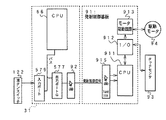
図6は、主制御基板31および音声を制御する制御手段としての音声制御基板70における信号送受信部分を示すブロック図である。この実施の形態では、遊技領域7の外側に設けられているスピーカ27の音声出力を指示するための音声再生用データが、主制御基板31から音声制御基板70に出力される。
【0034】
図6に示すように、音声再生用データは、基本回路53におけるI/Oポート部57の出力ポート575から出力される。音声制御基板70において、主制御基板31からの各信号は、バッファ回路705を介して音声制御用CPU701に入力する。なお、音声制御用CPU701がI/Oポートを内蔵していない場合には、バッファ回路705と音声制御用CPU701との間に、I/Oポートが設けられる。そして、例えばディジタルシグナルプロセッサによる音声合成回路702は、音声制御用CPU701の指示に応じた音声や効果音を発生し音量切替回路703に出力する。音量切替回路703は、音声制御用CPU701の出力レベルを、設定されている音量に応じたレベルにして音量増幅回路704に出力する。音量増幅回路704は、増幅した音声信号をスピーカ27に出力する。なお、主制御基板31において、出力ポート575の外側に信号伝達方向規制手段としてのバッファ回路71が設けられている。
【0035】
音声制御基板70において、音声制御用CPU701は、各音声再生用データに応じて定義されている音声/効果音パターンに従って、音声合成回路702に音声を出力させる。なお、音声/効果音パターンはROMに記憶されている。
【0036】
バッファ回路705として、例えば、汎用のCMOS−ICである74HC244が用いられる。74HC244のイネーブル端子には、常にローレベル(GNDレベル)が与えられている。よって、各バッファの出力レベルは、入力レベルすなわち主制御基板31からの信号レベルに確定している。従って、音声制御基板70側から主制御基板31側に信号が伝わる余地はない。たとえ、音声制御基板70内の回路に不正改造が加えられても、不正改造によって出力される信号が主制御基板31側に伝わることはない。
【0037】
図7は、主制御基板31および玉払出制御を行う制御手段としての賞球基板37における信号送受信部分を示すブロック図である。図7に示すように、賞球個数信号および賞球可能信号が、基本回路53におけるI/Oポート部57の出力ポート576から賞球基板37に出力される。賞球基板37において、主制御基板31からの各信号は、バッファ回路375を介して賞球制御用CPU371に入力する。なお、賞球制御用CPU371がI/Oポートを内蔵していない場合には、バッファ回路375と賞球制御用CPU371との間に、I/Oポートが設けられる。また、主制御基板31において、出力ポート576の外側に信号伝達方向規制手段としてのバッファ回路61が設けられている。
【0038】
図7には、賞球制御に関わる入賞球検出スイッチ99、玉切れスイッチ121、余剰玉受皿4における遊技球満杯を検出する満タンスイッチ122、および払い出される賞球をカウントする賞球カウントスイッチ123も示されている。入賞球検出スイッチ99、玉切れスイッチ121、満タンスイッチ122および賞球カウントスイッチ123の検出信号は、基本回路53におけるI/Oポート部57の入力ポート579を介してCPU56に入力する。CPU56は、玉切れスイッチ121がオンしたとき、および満タンスイッチ122がオンしたときに賞球可能信号をオフにする。また、基本回路53は、入賞球検出スイッチ99がオンすると、所定個の賞球を示す賞球個数信号を出力する。
【0039】
賞球基板37において、賞球制御用CPU371は、賞球個数信号が入力されると、I/Oポート372を介して玉払出装置97の賞球モータを駆動して指定された個数の遊技球を景品玉として払い出す。また、カードユニット50から玉貸し信号が入力されると、玉払出装置97の玉貸しモータを駆動して所定個の遊技球を払い出す。
【0040】
バッファ回路375として、例えば、汎用のCMOS−ICである74HC244が用いられる。74HC244のイネーブル端子には、常にローレベル(GNDレベル)が与えられている。よって、各バッファの出力レベルは、入力レベルすなわち主制御基板31からの信号レベルに確定している。従って、賞球基板37側から主制御基板31側に信号は伝わらない。たとえ、賞球基板37内の回路に不正改造が加えられても、不正改造によって出力される信号が主制御基板31側に伝わることはない。
【0041】
図8は、主制御基板31および打球発射を制御する制御手段としての発射制御基板91における信号送受信部分を示すブロック図である。図8に示すように、発射制御信号が、基本回路53におけるI/Oポート部57の出力ポート577から発射制御基板91に出力される。発射制御基板91において、主制御基板31からの発射制御信号は、バッファ回路915を介して発射制御用CPU911に入力する。なお、発射制御用CPU911がI/Oポートを内蔵していない場合には、バッファ回路915と発射制御用CPU911との間に、I/Oポートが設けられる。また、図8には、遊技球の発射制御に関わる満タンスイッチ122も示されている。打球供給皿3の裏面に設置されている満タンスイッチ122がオンすると、基本回路53は、発射制御信号をオフ状態にする。主制御基板31において、出力ポート577の外側に信号伝達方向規制手段としてのバッファ回路92が設けられている。
【0042】
発射制御用CPU911は、例えば、遊技球を発射する球打ち動作および次の玉を発射する準備である復旧・球補給動作の各期間における駆動モータ94の回転速度を制御する電圧を発生する。球打ち動作期間では、操作ノブ5に対する回転操作角に対応して徐々に増加する電圧を発生し、復旧・球補給動作期間では、あらかじめ定められた所定の電圧を発生する。
【0043】
タッチセンサ回路(図8において図示せず)は、操作ノブ5に取り付けられた人体検出用の電極(タッチセンサ)93に人体が接触している間、発射許可信号を発射制御用CPU911に出力する。また、発射制御用CPU911には、主制御基板31からの発射制御信号が与えられる。発射制御用CPU911は、発射制御信号および発射許可信号がオンすると、球打ち動作期間および復旧・球補給動作期間のシーケンス動作の切り替えを制御するとともに、駆動モータ94の駆動に必要な駆動パターン信号および駆動電圧切替信号を発生する。
【0044】
バッファ回路915として、例えば、汎用のCMOS−ICである74HC244が用いられる。74HC244のイネーブル端子には、常にローレベル(GNDレベル)が与えられている。よって、各バッファの出力レベルは、入力レベルすなわち主制御基板31からの信号レベルに確定している。従って、発射制御基板91側から主制御基板31側に信号は伝わらない。たとえ、発射制御基板91内の回路に不正改造が加えられても、不正改造によって出力される信号が主制御基板31側に伝わることはない。
【0045】
図9は、各基板間の主要な信号の流れと直流電力供給の様子を示すブロック図である。
図9に示すように、電源基板150には、外部から交流電力が供給される。この例ではAC24Vの交流電力が供給される。電源基板150には、AC24Vから、例えば、DC30V、DC21V、DC12Vを作成する電源回路が搭載されている。そして、各直流電圧とAC24Vとのうちの必要な電圧を、電源スイッチ151を介して、主制御基板31、ランプ制御基板35、賞球基板37、音声制御基板70、表示制御基板80および発射制御基板91に供給する。なお、図9に示された構成例では、主制御基板31と遊技用部品との間に主制御基板31Aが設けられている。
【0046】
図10は、電源基板150から、各基板に供給される直流電圧を示すブロック図である。図10に示すように、電源基板150には各種直流電圧を生成する電源回路152が搭載される。そして、各基板に供給される電力は、電源スイッチ151を介して供給される。なお、図10には、直流電圧のみが示されているが、必要に応じて、AC24Vも各基板に供給される。
【0047】
この実施の形態では、主制御基板31には、DC30VおよびDC12Vが供給される。ランプ制御基板35には、DC30V、DC21VおよびDC12Vが供給される。賞球基板37には、DC30VおよびDC12Vが供給される。音声制御基板70には、DC12Vが供給される。そして、発射制御基板91には、DC30VおよびDC12Vが供給される。なお、表示制御基板80には、主制御基板31を介して、DC30VおよびDC5Vが供給される。後述するように、表示制御基板80に供給されるDC5Vは、主制御基板31において作成される。
【0048】
図10に示すように、各基板に供給される電圧のグラウンド側は電源基板150において共通にとられている。従って、各基板におけるグラウンドレベルは共通である。すると、ある基板から他の基板に伝達される信号として、電圧レベルをそのまま使用することができる。グラウンドレベルが共通化されていない基板があると、そのような基板に対する信号伝達を行う場合には、フォトカプラ等の非接触式の情報伝達手段を用いる必要がありコストアップの要因となる。しかし、この実施の形態のように、全ての基板のグラウンドレベルが共通化されている場合には、フォトカプラ等を用いる必要はない。また、電源回路152から各基板に至る各電圧の電力は電源スイッチ151を介して供給されるので、遊技機に故障が生じたような場合には、直ちに全ての基板への電力供給を止めることができる。
【0049】
次に遊技機の動作について簡単に説明する。
図11は、主制御基板31における基本回路53のメイン動作を示すフローチャートである。上述したように、この処理は、定期リセット回路66が発するリセットパルスによって、例えば2ms毎に起動される。基本回路53が起動されると、基本回路53は、まず、スタックポインタの指定アドレスをセットするためのスタックセット処理を行う(ステップS1)。次いで、初期化処理を行う(ステップS2)。初期化処理では、基本回路53は、電源投入時か否か判定し、電源投入時にはRAM55を初期化する処理を行う。また、パチンコ遊技機1の内部に備えられている自己診断機能によって種々の異常診断処理が行われ、その結果に応じて必要ならば警報が発せられる(エラー処理:ステップS3)。
【0050】
次いで、大当り判定用乱数等の各判定用乱数を作成するための処理を行う。具体的には、各乱数を作成するためのカウンタを更新する処理を行う(ステップS4)。基本回路53は、さらに、図柄用乱数を作成する処理を行う(ステップS5)。すなわち、可変表示部9に表示される図柄の停止図柄を決定するための乱数等を更新(1加算)する処理を行う。
【0051】
次に、基本回路53は、普通図柄処理を行う(ステップS6)。普通図柄処理では、可変表示器10に表示される図柄を所定の順序で表示制御するための普通図柄プロセスフラグに従って該当する処理が選び出されて実行される。また、特別図柄処理を行う(ステップS7)。特別図柄処理では、遊技状態に応じてパチンコ遊技機1を所定の順序で制御するための特別図柄プロセスフラグに従って該当する処理が選び出されて実行される。そして、特別図柄プロセスフラグの値は、遊技状態に応じて各処理中に更新される。
【0052】
さらに、基本回路53は、遊技効果処理を行う(ステップS8)。遊技効果処理では、遊技効果LED28a、遊技効果ランプ28b,28cおよび装飾ランプ25を点灯/滅灯制御するランプ処理、遊技進行に応じてスピーカ27から所定音を発声させる音声処理が実行される。次に、基本回路31は、外部接続端子処理を行う(ステップS9)。外部接続端子処理では、情報出力回路64を介して、ホール管理用コンピュータに大当り情報、始動情報、確率変動情報などのデータを送信するための処理を行う。
【0053】
次いで、基本回路53は、賞球処理を行う(ステップS10)。賞球処理では、基本回路53は、入賞球検出スイッチ99からの入賞球信号を監視する。入賞球信号がオンすると、始動口スイッチ17がオンしていた場合には賞球個数信号に「6」をセットして賞球基板37に送出し、カウントスイッチ23またはVカウントスイッチ22がオンしていた場合には賞球個数信号に「15」をセットして賞球基板37に送出し、それらのスイッチがオンしていない場合には賞球個数信号に「10」をセットして賞球基板37に送出する。
【0054】
その後、基本回路53は、次に定期リセット回路65からリセットパルスが与えられるまで、ステップS11の図柄用乱数作成処理を繰り返す。すなわち、各乱数の値の1加算を行う。
【0055】
図12は、主制御基板31における電源供給と各遊技用構成機器に対する信号のやりとりの様子を示すブロック図である。図12に示すように、電源基板150からのDC30Vは、ソレノイド16,21を駆動するために使用される。また、DC12Vは、ゲートスイッチ12、始動口スイッチ17、Vカウントスイッチ22、カウントスイッチ23、入賞球検出スイッチ99、可変表示器10および始動入賞記憶表示器18に供給される。また、各スイッチからの信号はI/Oポート57を介して入力され、各表示器およびソレノイドへの信号はI/Oポート57を介して出力される。
【0056】
さらに、この実施の形態では、主制御基板31には、DC12VからDC5Vを作成するDC−DCコンバータ69が搭載されている。DC−DCコンバータ69が作成したDC5Vは、主制御基板31内のIC駆動電源となる。
【0057】
図13は、賞球基板37における電源供給と各遊技用構成機器に対する信号のやりとりの様子を示すブロック図である。電源基板150からのDC30Vは、玉払出装置97における賞球モータおよび玉貸しモータの駆動電源となる。また、DC12Vは、玉払出装置97における賞球カウントスイッチ123および玉貸しカウントスイッチ124に供給される。各スイッチからの信号はI/Oポート371を介して入力される。さらに、この実施の形態では、賞球基板37には、DC12VからDC5Vを作成するDC−DCコンバータ379が搭載されている。DC−DCコンバータ379が作成したDC5Vは、賞球基板37内のIC駆動電源となる。
【0058】
図14は、発射制御基板91における電源供給の様子を示すブロック図である。図14に示すように、電源基板150からのDC30Vは、遊技球を打撃して発射する打球発射装置を駆動する駆動モータ94の電源となる。また、この実施の形態では、発射制御基板91には、DC12VからDC5Vを作成するDC−DCコンバータ919が搭載されている。DC−DCコンバータ919が作成したDC5Vは、発射制御基板91内のIC駆動電源となる。
【0059】
図15は、ランプ制御基板35における電源供給の様子を示すブロック図である。図15に示すように、電源基板150からのDC30Vは、例えば、遊技効果LED28aを駆動するために使用される。また、DC21Vは、装飾ランプ25、遊技効果ランプ28b,28c、賞球ランプ51および玉切れランプ52を駆動するために使用される。DC12Vは、遊技盤面に設けられているLEDを駆動するために使用される。各ランプおよびLEDへの信号はI/Oポート357を介して出力される。また、ランプ制御基板35には、DC12VからDC5Vを作成するDC−DCコンバータ359が搭載されている。DC−DCコンバータ359が作成したDC5Vは、ランプ制御基板35内のIC駆動電源となる。
【0060】
図16は、図6に示された音声制御基板70の詳細な構成例を示すブロック図である。図16に示すように、電源基板150から供給されるDC12Vは、音量増幅回路704における増幅器741,742において増幅器電源として使用される。また、音声制御基板70には、DC12VからDC5Vを作成するDC−DCコンバータ709が搭載されている。DC−DCコンバータ709が作成したDC5Vは、音声制御基板70内のIC駆動電源となる。
【0061】
図16に示された構成例では、図6に示されたCPU701および音声合成回路702を実現するものとして、音声合成用LSI710と音声データROM712が用いられている。音声データROM712は、ICソケット713を介して音声制御基板70に実装される。音声合成用LSI710は、ディジタルシグナルプロセッサ機能を内蔵し、音声データROM712に格納されているデータにもとづいて音声や効果音に対応した音声信号を作成する。
【0061】
図16に示すように、この実施の形態では、主制御基板31から、転送リクエスト信号(SIRQ)、シリアルクロック信号(SICK)、シリアルデータ信号(SI)および転送終了信号(SRDY)が出力される。音声合成用LSI710は、SIRQがローレベルになると、SICKに同期してSIを1ビットずつ取り込み、SRDYがローレベルになるとそれまでに受信した各SIからなるデータを1つの音声再生用データと解釈する。なお、音声再生用データは例えば16ビットからなり、2msの間に1つの音声再生用データが出力される。
【0062】
主制御基板31における基本回路53は、遊技進行の各状態に応じて音声再生用データを出力する。メイン基板31の基本回路53は、ステップS8(図11参照)の遊技効果処理において、遊技進行の各状態に応じて音声再生用データを出力する。なお、音声再生用データの出力の要求は、特別図柄プロセス処理等で設定される。
【0063】
音声合成用LSI710は、受信した音声再生用データに応じて音声データROM712から該当データを入力し、入力したデータを信号処理して音声信号を作成する。そして、音声合成用LSI710からの音声信号は、音量切替回路703に出力される。
【0064】
音量切替回路703には、音量切替スイッチ731が設けられている。この実施の形態では、音量切替スイッチ731は、スライドスイッチ732、左スピーカ用の接点a1〜i1、左スピーカ用の抵抗R11,R12、右スピーカ用の接点a2〜i2、および右スピーカ用の抵抗R21,R22を含む。図16に示されたスイッチ状態では、音声合成用LSI710からの音声信号は、抵抗R11,R12,R21,R22を介さずに出力される。従って、音声合成用LSI710からの音声信号は、減衰を受けずに音量増幅回路704に出力される。
【0065】
スライドスイッチ732が1段階右にスライドされると、音声合成用LSI710からの音声信号(L)は、接点b1,gi,f1、スライドスイッチ732、接点h1,c1、および抵抗R11を介して出力される。従って、音声合成用LSI710からの音声信号(L)は、抵抗R11で減衰されて音量増幅回路704に出力される。すなわち、出力音量は低下する。同様に、音声信号(R)も、抵抗R21で減衰されて音量増幅回路704に出力される。さらに、スライドスイッチ732が右にスライドされると、音声信号(L)は抵抗R12で減衰され、音声信号(R)は抵抗R22で減衰される。
【0066】
音量増幅回路704において、増幅器741,742は、音量切替回路703からの音声信号(L),音声信号(R)を一定の増幅率で増幅し、スピーカ27に出力する。
以上のようにして、音声合成用LSI710によって生成された音声や効果音は、音量切替回路703におけるスイッチ設定に応じて音量調整された後に音量増幅回路704で増幅され、スピーカ27から放音される。
【0067】
この実施の形態では、音声制御基板70が主制御基板31とは別に設けられているので、主制御基板31のハードウェアが変更されたとしても、音声制御部分を変更せずにそのまま使用することができる。また、音声制御部分のハードウェアが変更されたとしても、その変更は主制御基板31のハードウェアに影響を与えない。よって、基板の再利用性が高まるとともに、遊技機の製造コストを下げることができる。
【0068】
さらに、音声制御基板70が主制御基板31とは別に設けられることによって、音声制御部分そのものの製造コストを下げることができる。音声制御部分を主制御基板31上に形成した場合には、音量切替回路703を搭載した基板(主制御基板31以外の基板)を設ける必要がある。主制御基板31は実際にはケースに覆われて遊技盤裏面に設置されるので、音量切替回路703を主制御基板31に搭載したのでは、スイッチ操作ができなくなってしまうからである。
【0069】
音声制御部分を主制御基板31上に形成し、音量切替回路703を別基板上に形成した場合には、音量切替回路703は、音量増幅回路704の後段に設置されることになる。すると、音量切替回路703には、増幅された音声信号が通過することになるので、音量切替回路703を構成する抵抗R11,R12,R21,R22を高電力に耐えるものとしなければならない。また、音量切替スイッチ731も高電力に耐えるものとしなければならない。従って、音量切替回路703の構成素子は高価なものになってしまう。しかし、この実施の形態によれば、音量切替回路703を音量増幅回路704の前段に設置することができるようになるので、音量切替回路703の構成素子として低電力タイプの安価なものを用いることができる。
【0070】
また、この実施の形態では、音声データROM712はICソケット713を介して音声制御基板70に実装されているので、容易に着脱することができる。従って、音声制御内容が変更された場合に、変更後の音声データが記憶された音声データROM712を容易に差し替えることができ、音声制御基板70のハードウェアを変更せずに済む。すなわち、遊技機に機種に応じた種々の音声制御を、1つの音声制御基板70のハードウェアで容易に実現することができる。
【0071】
また、音声制御部分の独立性を保証するために、音声制御部分は、機種変更に応じて変更される可能性が高い基板とは独立して設けられている必要がある。例えば、表示制御基板80は変更される可能性が比較的大きいので、音声制御部分は、少なくとも、表示制御基板80とは別に設けられていることが望ましい。
【0072】
図17は、主制御基板31から表示制御基板80に送信される表示制御コマンドデータを示す説明図である。また、図18は、表示制御基板80における電源供給の様子を示すブロック図である。図17に示すように、この実施の形態では、表示制御コマンドデータは、表示制御信号CD0〜CD7の8本の信号線で主制御基板31から表示制御基板80に送信される。また、主制御基板31と表示制御基板80との間には、表示制御コマンドデータの出力を示すストローブ信号を送信するための表示制御信号INTの信号線も配線されている。そして、表示制御基板80の電源となるDC5Vおよび可変表示部9に供給されるDC30Vの供給線、およびグラウンドレベルを供給するための信号線も配線されている。なお、DC5Vは、主制御基板31におけるDC−DCコンバータ69が作成したものである。
【0073】
上述したように、この実施の形態では、各基板上のICの電源となるDC5Vは、それぞれの基板において作成される。DC5Vを電源回路150で作成し各基板に供給すると、DC5V電源線が共通化されることになるので、基板間で電源線にノイズがのってICが誤動作する可能性がある。しかし、この実施の形態のように、各基板においてDC5Vを作成すれば、基板上のICが誤動作する可能性は大幅に低減する。また、表示制御基板80で使用する電源は主制御基板31を介して供給されているので、可変表示部9の構成変更にも容易に対応できる。
【0074】
上記の実施の形態では、主制御基板31、ランプ制御基板35、賞球基板37、音声制御基板70および発射制御基板91に搭載されたDC−DCコンバータ69,359,379,709,919は、電源基板150からのDC12VからDC5Vを作成した。しかし、電源基板150における電源回路152がDC12V以外の電圧を作成し、各基板は、その電圧からDC5Vを作成してもよい。
【0075】
図19は、電源基板150における電源回路152がDC30V、DC21V、DC12VおよびDC7Vを作成し、各基板は、DC7VからDC5Vを作成する例を示すブロック図である。DC12Vは、音声制御基板70においてスピーカ27の音量増幅用に使用されている。すると、音量増幅時に大きな電流が流れることによって、DC12Vの電圧値が変動する可能性もある。従って、DC12VからDC5Vを作成する場合には、DC12Vの変動が5V電源のノイズとして現れる可能性がある。しかし、電源基板150において、DC12Vとは異なる電圧を作成し、その電圧にもとづいて、各基板においてIC駆動用のDC5Vを作成すれば、より安定した5V電源を作成することができる。
【0076】
以上のように、上記の各実施の形態では、遊技機に搭載される各基板において使用される各電圧(DC5V以外)が、枠2A側の所定位置に設置された電源基板150で一括して作成され各基板に供給される。なお、図2に示された例では、所定位置は、枠2Aの裏面上部右側である。よって、機種変更される場合に、電源基板150を交換する必要はなく、コストダウンおよび基板の長寿命化を図ることができる。また、各基板において使用される各電圧が電源基板150で一括して作成されるので、DC5V以外の同一電圧作成のためのDC−DCコンバータを各基板に重複設置する必要はない。また、本発明によれば、各基板における発熱が低減される効果もある。さらに、各基板において使用される各電圧のうちIC駆動用電圧は各基板において作成されるのでIC誤動作が防止される。
【0077】
なお、上記の各実施の形態における基板構成(主制御基板31、ランプ制御基板35、賞球基板37、音声制御基板70および発射制御基板91)すなわち各制御手段の構成は一例であって、遊技機の形態に応じた他の構成がとられた場合であっても本発明を適用することができる。
【0078】
【発明の効果】
以上のように、本発明によれば、遊技機を、音声制御基板が少なくとも遊技制御基板および表示制御基板とは別に設けられ、音声制御基板に音量切替手段を搭載した構成にしたので、遊技機の製造コストを下げることができるとともに基板の長寿命化を図ることができる効果がある。
【0079】
音量切替手段が、音声制御基板に搭載されている音量増幅手段よりも前段に配置されている場合には、音量切替手段の構成素子として低電力タイプの安価なものを用いることができ、遊技機の製造コストを下げることができる。
また、音声データを記憶している音声データ記憶手段が、音声制御基板に着脱可能に搭載されている場合には、遊技機に機種に応じた種々の音声制御を、音声制御基板のハードウェアを変更せずに実現することができる。
【図面の簡単な説明】
【図1】 パチンコ遊技機を正面からみた正面図である。
【図2】 パチンコ遊技機の裏面に配置されている各基板を示す説明図である。
【図3】 パチンコ遊技機の遊技盤を背面からみた背面図である。
【図4】 主制御基板における回路構成の一例を示すブロック図である。
【図5】 主制御基板およびランプ制御基板における信号送受信部分を示すブロック図である。
【図6】 主制御基板および音声制御基板における信号送受信部分を示すブロック図である。
【図7】 主制御基板および賞球基板における信号送受信部分を示すブロック図である。
【図8】 主制御基板および発射制御基板における信号送受信部分を示すブロック図である。
【図9】 各基板間の主要な信号の流れと直流電力供給の様子を示すブロック図である。
【図10】 電源基板から各基板に供給される直流電圧を示すブロック図である。
【図11】 基本回路のメイン処理を示すフローチャートである。
【図12】 主制御基板における電源供給と信号のやりとりの様子を示すブロック図である。
【図13】 賞球基板における電源供給と信号のやりとりの様子を示すブロック図である。
【図14】 発射制御基板における電源供給の様子を示すブロック図である。
【図15】 ランプ制御基板における電源供給の様子を示すブロック図である。
【図16】 音声制御基板70の詳細な構成例を示すブロック図である。
【図17】 主制御基板から表示制御基板に送信される表示制御コマンドデータを示す説明図である。
【図18】 表示制御基板における電源供給の様子を示すブロック図である。
【図19】 電源基板から各基板に供給される直流電圧を示すブロック図である。
【符号の説明】
9 可変表示部
31 遊技制御基板(主制御基板)
35 ランプ制御基板
37 賞球基板
53 基本回路
70 音声制御基板
80 表示制御基板
91 発射制御基板
150 電源基板
151 電源スイッチ
152 電源回路
703 音量切替回路
704 音量増幅回路
710 音声合成用LSI
712 音声データROM
713 ICソケット
731 音量切替スイッチ[0001]
BACKGROUND OF THE INVENTION
The present invention relates to a gaming machine such as a pachinko gaming machine or a coin gaming machine in which a game is performed in accordance with a player's operation, and more particularly to a gaming machine in which a game is performed in accordance with a player's operation in a gaming area on a gaming board. .
[0002]
[Prior art]
A specific game that is advantageous to the player when a variable display device having a variable display unit capable of changing the display state is provided as a gaming machine, and the display result of the variable display unit becomes a predetermined specific display mode Some are configured to transition to a state. The variable display device has a plurality of variable display units, and is usually configured to display the display results of the plurality of variable display units at different times. For example, a plurality of pieces of identification information such as symbols are variably displayed on the variable display section. That the display result of the variable display unit is a combination of specific display modes determined in advance is usually referred to as “big hit”. Note that the game value is the right that the state of the variable winning ball device provided in the gaming area of the gaming machine is advantageous for a player who is likely to win a ball, or the advantageous state for a player. It is to generate.
[0003]
When the big hit occurs, for example, the big winning opening is opened a predetermined number of times, and the game shifts to a big hit gaming state where the hit ball is easy to win. And in each open period, if there is a prize for a predetermined number (for example, 10) of the big prize opening, the big prize opening is closed. And the number of times the special winning opening is opened is fixed to a predetermined number (for example, 15 rounds). An opening time (for example, 29.5 seconds) is determined for each opening, and even if the number of winnings does not reach a predetermined number, the big winning opening is closed when the opening time elapses. Further, when a predetermined condition (for example, winning in the V zone provided in the big prize opening) is not established at the time when the big prize opening is closed, the big hit gaming state is ended.
[0004]
The progress of the game including the occurrence of a big hit is controlled by a game control microcomputer circuit mounted on a game control board (main control board) installed on the back side of the game board. In addition, lamps, LEDs, speakers, and the like are installed on the game board surface and inside the frame to enhance the game effect. A board on which a circuit for performing such on / off control is mounted is also installed on the back side of the game board. Also, a display control board equipped with each circuit for controlling the display of the variable display unit for generating a big hit, a firing control board equipped with each circuit for controlling the firing of the hit ball, and a payout control of the prize balls and the balls are performed. A prize ball board is also installed on the back of the game board.
[0005]
The speaker is controlled by a game control microcomputer circuit mounted on the main control board, but is driven by a voltage different from 5 V which is the operating voltage of the microcomputer circuit. Thus, the necessary current amplification is performed on the main control board. The speaker is generally installed on the frame side of the gaming machine. In general, a lamp and an LED for enhancing the gaming effect are also installed on the frame side of the gaming machine. Therefore, the signal lines to the lamp, the LED, and the speaker are wired on the frame side through one electric decoration board (generally, a circuit for amplifying the lamp and the LED is mounted). In addition, a volume adjustment switch is provided to adjust the volume of the speakers in accordance with the installation situation of the gaming machine, but the volume adjustment switch is installed on an electric decoration board that serves as a path for audio signals.
[0006]
[Problems to be solved by the invention]
Since the conventional gaming machine is configured as described above, if the voice control is changed when changing the model, the main control board may have to be recreated. Further, when the installation position and type of the volume adjustment switch are changed, there is a case where it is necessary to remake the illumination board even if the lamp and the LED are not changed. That is, in a conventional gaming machine, a change related to voice control may cause the main control board or the like to be rebuilt. As a result, there is a limit to reducing the manufacturing cost of the gaming machine.
[0007]
The present invention has been made to solve such a problem, and an object of the present invention is to provide a gaming machine capable of reducing the manufacturing cost and extending the life of the board.
[0008]
[Means for Solving the Problems]
A gaming machine according to the present invention has a gaming control board on which a gaming area is provided in a gaming board, a game is played in accordance with a player's operation, and game controlling means for controlling the progress of the game is mounted, and from the gaming control board. A game machine including a display control board on which display control means for performing display control of a variable display unit provided on a game board based on a signal is provided, and provided at least separately from the game control board and the display control board Voice control board that controls voice based on information from the game control board A power supply board for supplying power to each board including a game control board and a voice control board; The voice control board is equipped with , Equipped with volume switching means The power supply board generates a supply power having a higher voltage than the drive power supply for driving the IC mounted on each board and supplies the power supply to each board. Each board supplies the drive power from the power supply board to each board. Drive power generation means for generating from the supplied power supply is installed. It is characterized by that.
[0009]
Here, the sound volume switching means may be arranged upstream of the sound volume amplifying means mounted on the sound control board.
The voice data storage means for storing voice data mounted on the voice control board may be detachably mounted on the voice control board.
[0010]
DETAILED DESCRIPTION OF THE INVENTION
Hereinafter, an embodiment of the present invention will be described with reference to the drawings.
First, the overall configuration of a pachinko gaming machine that is an example of a gaming machine will be described. FIG. 1 is a front view of the
[0011]
As shown in FIG. 1, the
[0012]
Near the center of the
[0013]
An open / close plate 20 that is opened by a solenoid 21 in a specific gaming state (big hit state) is provided below the variable winning ball device 15. In this embodiment, the opening / closing plate 20 is a means for opening and closing the special winning opening. Of the winning balls guided from the opening / closing plate 20 to the back of the
[0014]
The
[0015]
The hit ball fired from the hit ball launching device enters the
[0016]
When the combination of images in the
Further, when the stop symbol on the
[0017]
Next, each board | substrate arrange | positioned at the back surface of the
As shown in FIG. 2, on the back surface of the
[0018]
The mechanism board is provided with a variable
[0019]
Furthermore, a
[0020]
FIG. 3 is a rear view of the game board of the
[0021]
In order to perform the winning ball payout control, signals from the winning
[0022]
FIG. 4 is a block diagram illustrating an example of a circuit configuration in the
[0023]
Further, according to the data given from the
[0024]
The
[0025]
Further, the
[0026]
A ball hitting device for hitting and launching a game ball is driven by a
[0027]
FIG. 5 is a block diagram showing signal transmission / reception portions in the
[0028]
As shown in FIG. 5, each signal related to lamp control is output from
[0029]
In the
[0030]
In the
[0031]
As the
[0032]
Accordingly, it is possible to eliminate a signal line that may give a signal from the
[0033]
FIG. 6 is a block diagram showing signal transmission / reception portions in the
[0034]
As shown in FIG. 6, the audio playback data is output from the
[0035]
In the
[0036]
As the
[0037]
FIG. 7 is a block diagram showing a signal transmission / reception portion in the
[0038]
FIG. 7 shows a winning
[0039]
In the
[0040]
As the
[0041]
FIG. 8 is a block diagram showing a signal transmission / reception portion in the
[0042]
For example, the firing control CPU 911 generates a voltage for controlling the rotational speed of the
[0043]
The touch sensor circuit (not shown in FIG. 8) outputs a firing permission signal to the firing control CPU 911 while the human body is in contact with the human body detection electrode (touch sensor) 93 attached to the
[0044]
As the
[0045]
FIG. 9 is a block diagram showing the main signal flow between the substrates and the state of DC power supply.
As shown in FIG. 9, AC power is supplied to the
[0046]
FIG. 10 is a block diagram showing a DC voltage supplied from the
[0047]
In this embodiment, the
[0048]
As shown in FIG. 10, the ground side of the voltage supplied to each substrate is commonly used in the
[0049]
Next, the operation of the gaming machine will be briefly described.
FIG. 11 is a flowchart showing the main operation of the
[0050]
Next, a process for creating each determination random number such as a big hit determination random number is performed. Specifically, a process for updating a counter for generating each random number is performed (step S4). The
[0051]
Next, the
[0052]
Further, the
[0053]
Next, the
[0054]
Thereafter, the
[0055]
FIG. 12 is a block diagram showing a state of power supply in the
[0056]
Further, in this embodiment, the
[0057]
FIG. 13 is a block diagram showing a state of power supply in the
[0058]
FIG. 14 is a block diagram showing a state of power supply in the
[0059]
FIG. 15 is a block diagram showing a state of power supply in the
[0060]
FIG. 16 is a block diagram showing a detailed configuration example of the
[0061]
In the configuration example shown in FIG. 16, a
[0061]
As shown in FIG. 16, in this embodiment, a transfer request signal (SIRQ), a serial clock signal (SICK), a serial data signal (SI), and a transfer end signal (SRDY) are output from the
[0062]
The
[0063]
The
[0064]
The
[0065]
When the slide switch 732 is slid to the right by one step, the audio signal (L) from the
[0066]
In the
As described above, the sound and sound effect generated by the
[0067]
In this embodiment, since the
[0068]
Furthermore, since the
[0069]
When the audio control part is formed on the
[0070]
In this embodiment, since the
[0071]
Further, in order to guarantee the independence of the voice control part, the voice control part needs to be provided independently of a board that is highly likely to be changed according to the model change. For example, since the
[0072]
FIG. 17 is an explanatory diagram showing display control command data transmitted from the
[0073]
As described above, in this embodiment, DC5V that is the power source of the IC on each substrate is created on each substrate. When DC5V is created by the
[0074]
In the above embodiment, the DC-
[0075]
FIG. 19 is a block diagram illustrating an example in which the
[0076]
As described above, in each of the above-described embodiments, each voltage (other than DC5V) used in each board mounted on the gaming machine is collectively collected by the
[0077]
It should be noted that the board configuration (
[0078]
【The invention's effect】
As described above, according to the present invention, the gaming machine is configured such that the voice control board is provided separately from at least the gaming control board and the display control board, and the volume control means is mounted on the voice control board. The manufacturing cost can be reduced and the life of the substrate can be extended.
[0079]
When the volume switching means is arranged in front of the volume amplification means mounted on the voice control board, a low-power type inexpensive device can be used as a component of the volume switching means. The manufacturing cost can be reduced.
In addition, when the voice data storage means storing voice data is detachably mounted on the voice control board, various voice controls according to the model are performed on the gaming machine by using the hardware of the voice control board. It can be realized without change.
[Brief description of the drawings]
FIG. 1 is a front view of a pachinko gaming machine as viewed from the front.
FIG. 2 is an explanatory diagram showing each substrate disposed on the back surface of the pachinko gaming machine.
FIG. 3 is a rear view of the game board of the pachinko gaming machine as viewed from the back.
FIG. 4 is a block diagram showing an example of a circuit configuration on a main control board.
FIG. 5 is a block diagram showing signal transmission / reception portions in the main control board and the lamp control board.
FIG. 6 is a block diagram showing signal transmission / reception portions in the main control board and the voice control board.
FIG. 7 is a block diagram showing signal transmission / reception portions on the main control board and the prize ball board.
FIG. 8 is a block diagram showing signal transmission / reception portions on the main control board and the launch control board.
FIG. 9 is a block diagram showing a main signal flow between substrates and a state of DC power supply.
FIG. 10 is a block diagram showing a DC voltage supplied from a power supply board to each board.
FIG. 11 is a flowchart showing main processing of the basic circuit.
FIG. 12 is a block diagram showing a state of power supply and signal exchange in the main control board.
FIG. 13 is a block diagram showing a state of power supply and signal exchange in a prize ball substrate.
FIG. 14 is a block diagram showing a state of power supply in the launch control board.
FIG. 15 is a block diagram showing a state of power supply in the lamp control board.
FIG. 16 is a block diagram showing a detailed configuration example of a
FIG. 17 is an explanatory diagram showing display control command data transmitted from the main control board to the display control board.
FIG. 18 is a block diagram showing a state of power supply in the display control board.
FIG. 19 is a block diagram showing a DC voltage supplied from a power supply substrate to each substrate.
[Explanation of symbols]
9 Variable display section
31 Game control board (main control board)
35 Lamp control board
37 prize ball board
53 Basic circuit
70 Voice control board
80 Display control board
91 Launch Control Board
150 Power supply board
151 Power switch
152 Power supply circuit
703 Volume switching circuit
704 Volume amplifier circuit
710 LSI for speech synthesis
712 Audio data ROM
713 IC socket
731 Volume switch
Claims (3)
少なくとも前記遊技制御基板および表示制御基板とは別に設けられ、前記遊技制御基板からの情報にもとづいて音声に関する制御を行う音声制御基板と、
前記遊技制御基板および前記音声制御基板を含む各基板に電源を供給する電源基板とを備え、
前記音声制御基板は、音量切替手段を搭載し、
前記電源基板は、前記各基板に搭載されているICを駆動するための駆動電源より電圧の高い供給電源を作成して前記各基板に供給し、
前記各基板は、前記駆動電源を前記電源基板から該各基板に供給される前記供給電源から生成する駆動電源生成手段をそれぞれ搭載している
ことを特徴とする遊技機。A game area is provided on the game board, a game is played in accordance with a player's operation, a game control board on which game control means for controlling the progress of the game is mounted, and the game based on a signal from the game control board A gaming machine including a display control board on which display control means for performing display control of a variable display unit provided on a board is mounted,
A voice control board that is provided separately from at least the game control board and the display control board, and performs control related to voice based on information from the game control board ;
A power supply board for supplying power to each board including the game control board and the voice control board ,
The voice control board is equipped with volume switching means ,
The power supply board creates a supply power having a higher voltage than a drive power supply for driving an IC mounted on each board and supplies the power supply to each board.
Each of the boards is equipped with a drive power generation means for generating the drive power from the power supply supplied from the power supply board to the boards .
請求項1記載の遊技機。The gaming machine according to claim 1, wherein the sound volume switching means is arranged upstream of the sound volume amplifying means mounted on the sound control board.
請求項1または請求項2記載の遊技機。The gaming machine according to claim 1 or 2, wherein voice data storage means for storing voice data is detachably provided on the voice control board.
Priority Applications (1)
| Application Number | Priority Date | Filing Date | Title |
|---|---|---|---|
| JP19655198A JP4255534B2 (en) | 1998-06-26 | 1998-06-26 | Game machine |
Applications Claiming Priority (1)
| Application Number | Priority Date | Filing Date | Title |
|---|---|---|---|
| JP19655198A JP4255534B2 (en) | 1998-06-26 | 1998-06-26 | Game machine |
Publications (3)
| Publication Number | Publication Date |
|---|---|
| JP2000014867A JP2000014867A (en) | 2000-01-18 |
| JP2000014867A5 JP2000014867A5 (en) | 2008-08-07 |
| JP4255534B2 true JP4255534B2 (en) | 2009-04-15 |
Family
ID=16359627
Family Applications (1)
| Application Number | Title | Priority Date | Filing Date |
|---|---|---|---|
| JP19655198A Expired - Lifetime JP4255534B2 (en) | 1998-06-26 | 1998-06-26 | Game machine |
Country Status (1)
| Country | Link |
|---|---|
| JP (1) | JP4255534B2 (en) |
Cited By (1)
| Publication number | Priority date | Publication date | Assignee | Title |
|---|---|---|---|---|
| JP2015093154A (en) * | 2013-11-14 | 2015-05-18 | 株式会社大一商会 | Game machine |
Families Citing this family (8)
| Publication number | Priority date | Publication date | Assignee | Title |
|---|---|---|---|---|
| JP2001211197A (en) * | 2000-01-26 | 2001-08-03 | Nec Corp | Communication system, communication method, gateway device and client |
| JP4576663B2 (en) * | 2000-04-26 | 2010-11-10 | 株式会社三洋物産 | Game machine |
| JP3957466B2 (en) * | 2001-03-27 | 2007-08-15 | 株式会社藤商事 | Bullet ball machine |
| JP3957465B2 (en) * | 2001-03-27 | 2007-08-15 | 株式会社藤商事 | Bullet ball machine |
| JP2003052981A (en) * | 2001-08-08 | 2003-02-25 | Heiwa Corp | Game machine |
| JP2006218091A (en) * | 2005-02-10 | 2006-08-24 | Daiman:Kk | Game machine |
| JP7257787B2 (en) * | 2018-12-28 | 2023-04-14 | 株式会社平和 | game machine |
| JP7261581B2 (en) * | 2018-12-28 | 2023-04-20 | 株式会社平和 | game machine |
-
1998
- 1998-06-26 JP JP19655198A patent/JP4255534B2/en not_active Expired - Lifetime
Cited By (1)
| Publication number | Priority date | Publication date | Assignee | Title |
|---|---|---|---|---|
| JP2015093154A (en) * | 2013-11-14 | 2015-05-18 | 株式会社大一商会 | Game machine |
Also Published As
| Publication number | Publication date |
|---|---|
| JP2000014867A (en) | 2000-01-18 |
Similar Documents
| Publication | Publication Date | Title |
|---|---|---|
| JPH11267275A (en) | Game machine | |
| JP2005058426A (en) | Game machine | |
| JP2896370B1 (en) | Gaming machine | |
| JP4255534B2 (en) | Game machine | |
| JP4065606B2 (en) | Game machine | |
| JP2004016300A (en) | Game machine | |
| JPH1147408A (en) | Game machine | |
| JPH11300011A (en) | Game machine | |
| JPH11299985A (en) | Game machine | |
| JP2002058837A (en) | Game machine | |
| JPH1147399A (en) | Game machine | |
| JPH11285576A (en) | Game machine | |
| JP2003284819A (en) | Game machine | |
| JP4420998B2 (en) | Game machine | |
| JP2002136687A (en) | Game machine | |
| JP2000312765A (en) | Game machine | |
| JP2004236671A (en) | Game machine | |
| JP2754015B2 (en) | Ball game machine | |
| JP2006296482A (en) | Game machine | |
| JP4528905B2 (en) | Bullet ball machine | |
| JP7401947B2 (en) | gaming machine | |
| JP2002126196A (en) | Game machine | |
| JP5574673B2 (en) | Game machine | |
| JP2001161908A (en) | Game machine | |
| JP2004129756A (en) | Game machine, program and recording medium |
Legal Events
| Date | Code | Title | Description |
|---|---|---|---|
| A621 | Written request for application examination |
Free format text: JAPANESE INTERMEDIATE CODE: A621 Effective date: 20050523 |
|
| RD03 | Notification of appointment of power of attorney |
Free format text: JAPANESE INTERMEDIATE CODE: A7423 Effective date: 20060119 |
|
| A521 | Written amendment |
Free format text: JAPANESE INTERMEDIATE CODE: A523 Effective date: 20080619 |
|
| A977 | Report on retrieval |
Free format text: JAPANESE INTERMEDIATE CODE: A971007 Effective date: 20081008 |
|
| A131 | Notification of reasons for refusal |
Free format text: JAPANESE INTERMEDIATE CODE: A131 Effective date: 20081014 |
|
| A521 | Written amendment |
Free format text: JAPANESE INTERMEDIATE CODE: A523 Effective date: 20081210 |
|
| TRDD | Decision of grant or rejection written | ||
| A01 | Written decision to grant a patent or to grant a registration (utility model) |
Free format text: JAPANESE INTERMEDIATE CODE: A01 Effective date: 20090120 |
|
| A01 | Written decision to grant a patent or to grant a registration (utility model) |
Free format text: JAPANESE INTERMEDIATE CODE: A01 |
|
| A61 | First payment of annual fees (during grant procedure) |
Free format text: JAPANESE INTERMEDIATE CODE: A61 Effective date: 20090128 |
|
| FPAY | Renewal fee payment (event date is renewal date of database) |
Free format text: PAYMENT UNTIL: 20120206 Year of fee payment: 3 |
|
| R150 | Certificate of patent or registration of utility model |
Free format text: JAPANESE INTERMEDIATE CODE: R150 |
|
| FPAY | Renewal fee payment (event date is renewal date of database) |
Free format text: PAYMENT UNTIL: 20120206 Year of fee payment: 3 |
|
| FPAY | Renewal fee payment (event date is renewal date of database) |
Free format text: PAYMENT UNTIL: 20120206 Year of fee payment: 3 |
|
| FPAY | Renewal fee payment (event date is renewal date of database) |
Free format text: PAYMENT UNTIL: 20120206 Year of fee payment: 3 |
|
| FPAY | Renewal fee payment (event date is renewal date of database) |
Free format text: PAYMENT UNTIL: 20130206 Year of fee payment: 4 |
|
| FPAY | Renewal fee payment (event date is renewal date of database) |
Free format text: PAYMENT UNTIL: 20130206 Year of fee payment: 4 |
|
| R250 | Receipt of annual fees |
Free format text: JAPANESE INTERMEDIATE CODE: R250 |
|
| R250 | Receipt of annual fees |
Free format text: JAPANESE INTERMEDIATE CODE: R250 |
|
| R250 | Receipt of annual fees |
Free format text: JAPANESE INTERMEDIATE CODE: R250 |
|
| R250 | Receipt of annual fees |
Free format text: JAPANESE INTERMEDIATE CODE: R250 |
|
| R250 | Receipt of annual fees |
Free format text: JAPANESE INTERMEDIATE CODE: R250 |
|
| EXPY | Cancellation because of completion of term |