JP4238877B2 - FFS mode LCD panel - Google Patents
FFS mode LCD panel Download PDFInfo
- Publication number
- JP4238877B2 JP4238877B2 JP2006088208A JP2006088208A JP4238877B2 JP 4238877 B2 JP4238877 B2 JP 4238877B2 JP 2006088208 A JP2006088208 A JP 2006088208A JP 2006088208 A JP2006088208 A JP 2006088208A JP 4238877 B2 JP4238877 B2 JP 4238877B2
- Authority
- JP
- Japan
- Prior art keywords
- liquid crystal
- crystal display
- display panel
- mode liquid
- scanning line
- Prior art date
- Legal status (The legal status is an assumption and is not a legal conclusion. Google has not performed a legal analysis and makes no representation as to the accuracy of the status listed.)
- Expired - Fee Related
Links
Images


Classifications
-
- G—PHYSICS
- G02—OPTICS
- G02F—OPTICAL DEVICES OR ARRANGEMENTS FOR THE CONTROL OF LIGHT BY MODIFICATION OF THE OPTICAL PROPERTIES OF THE MEDIA OF THE ELEMENTS INVOLVED THEREIN; NON-LINEAR OPTICS; FREQUENCY-CHANGING OF LIGHT; OPTICAL LOGIC ELEMENTS; OPTICAL ANALOGUE/DIGITAL CONVERTERS
- G02F1/00—Devices or arrangements for the control of the intensity, colour, phase, polarisation or direction of light arriving from an independent light source, e.g. switching, gating or modulating; Non-linear optics
- G02F1/01—Devices or arrangements for the control of the intensity, colour, phase, polarisation or direction of light arriving from an independent light source, e.g. switching, gating or modulating; Non-linear optics for the control of the intensity, phase, polarisation or colour
- G02F1/13—Devices or arrangements for the control of the intensity, colour, phase, polarisation or direction of light arriving from an independent light source, e.g. switching, gating or modulating; Non-linear optics for the control of the intensity, phase, polarisation or colour based on liquid crystals, e.g. single liquid crystal display cells
- G02F1/133—Constructional arrangements; Operation of liquid crystal cells; Circuit arrangements
- G02F1/1333—Constructional arrangements; Manufacturing methods
- G02F1/1343—Electrodes
- G02F1/134309—Electrodes characterised by their geometrical arrangement
- G02F1/134363—Electrodes characterised by their geometrical arrangement for applying an electric field parallel to the substrate, i.e. in-plane switching [IPS]
-
- G—PHYSICS
- G02—OPTICS
- G02F—OPTICAL DEVICES OR ARRANGEMENTS FOR THE CONTROL OF LIGHT BY MODIFICATION OF THE OPTICAL PROPERTIES OF THE MEDIA OF THE ELEMENTS INVOLVED THEREIN; NON-LINEAR OPTICS; FREQUENCY-CHANGING OF LIGHT; OPTICAL LOGIC ELEMENTS; OPTICAL ANALOGUE/DIGITAL CONVERTERS
- G02F1/00—Devices or arrangements for the control of the intensity, colour, phase, polarisation or direction of light arriving from an independent light source, e.g. switching, gating or modulating; Non-linear optics
- G02F1/01—Devices or arrangements for the control of the intensity, colour, phase, polarisation or direction of light arriving from an independent light source, e.g. switching, gating or modulating; Non-linear optics for the control of the intensity, phase, polarisation or colour
- G02F1/13—Devices or arrangements for the control of the intensity, colour, phase, polarisation or direction of light arriving from an independent light source, e.g. switching, gating or modulating; Non-linear optics for the control of the intensity, phase, polarisation or colour based on liquid crystals, e.g. single liquid crystal display cells
- G02F1/133—Constructional arrangements; Operation of liquid crystal cells; Circuit arrangements
- G02F1/1333—Constructional arrangements; Manufacturing methods
- G02F1/1337—Surface-induced orientation of the liquid crystal molecules, e.g. by alignment layers
- G02F1/133707—Structures for producing distorted electric fields, e.g. bumps, protrusions, recesses, slits in pixel electrodes
-
- G—PHYSICS
- G02—OPTICS
- G02F—OPTICAL DEVICES OR ARRANGEMENTS FOR THE CONTROL OF LIGHT BY MODIFICATION OF THE OPTICAL PROPERTIES OF THE MEDIA OF THE ELEMENTS INVOLVED THEREIN; NON-LINEAR OPTICS; FREQUENCY-CHANGING OF LIGHT; OPTICAL LOGIC ELEMENTS; OPTICAL ANALOGUE/DIGITAL CONVERTERS
- G02F1/00—Devices or arrangements for the control of the intensity, colour, phase, polarisation or direction of light arriving from an independent light source, e.g. switching, gating or modulating; Non-linear optics
- G02F1/01—Devices or arrangements for the control of the intensity, colour, phase, polarisation or direction of light arriving from an independent light source, e.g. switching, gating or modulating; Non-linear optics for the control of the intensity, phase, polarisation or colour
- G02F1/13—Devices or arrangements for the control of the intensity, colour, phase, polarisation or direction of light arriving from an independent light source, e.g. switching, gating or modulating; Non-linear optics for the control of the intensity, phase, polarisation or colour based on liquid crystals, e.g. single liquid crystal display cells
- G02F1/133—Constructional arrangements; Operation of liquid crystal cells; Circuit arrangements
- G02F1/1333—Constructional arrangements; Manufacturing methods
- G02F1/1343—Electrodes
- G02F1/134309—Electrodes characterised by their geometrical arrangement
- G02F1/134372—Electrodes characterised by their geometrical arrangement for fringe field switching [FFS] where the common electrode is not patterned
-
- G—PHYSICS
- G02—OPTICS
- G02F—OPTICAL DEVICES OR ARRANGEMENTS FOR THE CONTROL OF LIGHT BY MODIFICATION OF THE OPTICAL PROPERTIES OF THE MEDIA OF THE ELEMENTS INVOLVED THEREIN; NON-LINEAR OPTICS; FREQUENCY-CHANGING OF LIGHT; OPTICAL LOGIC ELEMENTS; OPTICAL ANALOGUE/DIGITAL CONVERTERS
- G02F2201/00—Constructional arrangements not provided for in groups G02F1/00 - G02F7/00
- G02F2201/12—Constructional arrangements not provided for in groups G02F1/00 - G02F7/00 electrode
- G02F2201/128—Constructional arrangements not provided for in groups G02F1/00 - G02F7/00 electrode field shaping
-
- G—PHYSICS
- G02—OPTICS
- G02F—OPTICAL DEVICES OR ARRANGEMENTS FOR THE CONTROL OF LIGHT BY MODIFICATION OF THE OPTICAL PROPERTIES OF THE MEDIA OF THE ELEMENTS INVOLVED THEREIN; NON-LINEAR OPTICS; FREQUENCY-CHANGING OF LIGHT; OPTICAL LOGIC ELEMENTS; OPTICAL ANALOGUE/DIGITAL CONVERTERS
- G02F2201/00—Constructional arrangements not provided for in groups G02F1/00 - G02F7/00
- G02F2201/40—Arrangements for improving the aperture ratio
Landscapes
- Physics & Mathematics (AREA)
- Nonlinear Science (AREA)
- Mathematical Physics (AREA)
- Chemical & Material Sciences (AREA)
- Crystallography & Structural Chemistry (AREA)
- General Physics & Mathematics (AREA)
- Optics & Photonics (AREA)
- Geometry (AREA)
- Spectroscopy & Molecular Physics (AREA)
- Liquid Crystal (AREA)
Description
本発明は、フリンジ・フィールド・スィッチング(Fringe Field Switching:以下、「
FFS」という。)モードの液晶表示パネルに関し、特に画素の配列をデルタ配置とした
デュアルドメイン構造のFFSモードの液晶表示パネルに関する。
The present invention relates to fringe field switching (hereinafter referred to as “Fringe Field Switching”).
FFS ". ) Mode liquid crystal display panel, and more particularly to an FFS mode liquid crystal display panel having a dual domain structure in which pixels are arranged in a delta arrangement.
近年、情報通信機器のみならず一般の電気機器においても液晶表示パネルが多く利用さ
れている。従来から多く用いられている液晶表示パネルは、表面に電極等が形成された一
対のガラス等からなる基板と、この一対の基板間に形成された液晶層と、からなり、両基
板上の電極に電圧が印加されることにより、液晶分子を再配列させて光の透過率を変える
ことにより種々の映像を表示する、言わば縦方向電界モードともいうべきものである。こ
のような縦方向電界モードの液晶表示パネルは、TN(Twisted Nematic)モードやVA
(Vertical Alignment)モードのもの存在するが、視野角が狭いという問題点が存在する
ため、MVA(Multidomain Vertical Alignment)モード等種々の改良された縦方向電界
モードの液晶表示パネルが開発されている。
In recent years, liquid crystal display panels are widely used not only in information communication equipment but also in general electric equipment. Conventionally used liquid crystal display panels are composed of a pair of glass substrates having electrodes formed on the surface thereof, and a liquid crystal layer formed between the pair of substrates, and electrodes on both substrates. When a voltage is applied to the liquid crystal, various images are displayed by rearranging the liquid crystal molecules and changing the light transmittance, which is to say a longitudinal electric field mode. Such a vertical electric field mode liquid crystal display panel has a TN (Twisted Nematic) mode or a VA mode.
Although there is a problem in the (Vertical Alignment) mode, there is a problem that the viewing angle is narrow. Therefore, various improved vertical electric field mode liquid crystal display panels such as an MVA (Multidomain Vertical Alignment) mode have been developed.
一方、上述の縦方向電界モードの液晶表示パネルとは異なり、一方の基板にのみ電極を
備えた横方向電界モードと言うべき液晶表示パネルも、IPS(In-Plane Switching)モ
ードの液晶表示パネルとして知られている(下記特許文献1参照)。ここでこのIPSモ
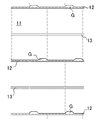
ードの液晶表示パネルの動作原理を図11及び図12を用いて説明する。なお、図11は
IPSモードの液晶表示パネルの1画素分の概略平面図であり、図12は図11のXII−X
II線に沿った概略断面図である。
On the other hand, unlike the above-described vertical electric field mode liquid crystal display panel, an IPS (In-Plane Switching) mode liquid crystal display panel, which should be referred to as a horizontal electric field mode having electrodes only on one substrate, is also used. It is known (see
It is a schematic sectional drawing along the II line.
このIPSモードの液晶表示パネル50は、アレイ基板ARとカラーフィルタ基板CF
とを備えている。アレイ基板ARは、第1の透明基板51の表面にそれぞれ平行に複数の
走査線52及びコモン配線53が設けられ、これら走査線52及びコモン配線53に直交
する方向に複数の信号線54が設けられている。そして、各画素の中央部にコモン配線5
3から帯状に、図11においては逆T字状に、対向電極55が設けられ、この対向電極5
5の周囲を囲むように画素電極56が設けられている。
The IPS mode liquid
And. In the array substrate AR, a plurality of
3, a
A
そして、走査線52と信号線54との間にはスイッチング素子としてのTFT(Thin F
ilm Transistor)が形成されている。このTFTは、走査線52と信号線54との間に半
導体層57が配置され、半導体層57上の信号線部分がTFTのソース電極Sを構成し、
半導体層57の下部の走査線部分がゲート電極Gを構成し、また、半導体層57の一部分
と重なる画素電極56の部分がドレイン電極Dを構成している。
A TFT (Thin F) serving as a switching element is provided between the
ilm Transistor) is formed. In this TFT, a
The scanning line portion below the
また、カラーフィルタ基板CFは、第二の透明基板58の表面にカラーフィルタ層59
が設けられた構成を有している。そして、アレイ基板ARの画素電極56及び対向電極5
5とカラーフィルタ基板CFのカラーフィルタ層59とが互いに対向するようにアレイ基
板AR及びカラーフィルタ基板CFを対向させ、その間に液晶LCを封入するとともに、
両基板のそれぞれ外側に偏光板60及び61を偏光方向が互いに直交する方向となるよう
に配置することにより、IPSモードの液晶表示パネル50が形成される。
Further, the color filter substrate CF has a
Is provided. Then, the
5 and the
The IPS mode liquid
このIPSモードの液晶表示パネル50は、図12に示したように、画素電極56と対
向電極55との間に電界を形成すると、水平方向に配向していた液晶分子が水平方向に旋
回することによりバックライトからの入射光の透過量を制御することができるようになる
。このIPSモードの液晶表示パネル50は、広視野角で、高コントラストであり、また
、画素電極56と対向電極55とが比較的狭い間隔で配置されているために保持容量が副
次的に生じるという長所があるが、対向電極55がコモン配線53と同じ金属材料で形成
されるために開口率及び透過率が低く、又、視角による色変化があるという問題点が存在
する。
In the IPS mode liquid
このようなIPSモードの液晶表示パネルの低開口率及び低透過率という問題点を解決
するために、いわゆる斜め電界方式とも言うべきFFSモードの液晶表示装置が開発され
ている(下記特許文献2〜4参照)。このFFSモードの液晶表示パネル動作原理を図1
3及び図14を用いて説明する。なお、図13はFFSモードの液晶表示パネルの1画素
分の概略平面図であり、図14は図13のXIV−XIV線に沿った概略断面図である。
In order to solve the problems of low aperture ratio and low transmittance of such an IPS mode liquid crystal display panel, an FFS mode liquid crystal display device that should be called a so-called oblique electric field method has been developed (Patent Documents 2 to 2 below). 4). The operation principle of the FFS mode liquid crystal display panel is shown in FIG.
3 and FIG. 13 is a schematic plan view for one pixel of the FFS mode liquid crystal display panel, and FIG. 14 is a schematic cross-sectional view taken along the line XIV-XIV in FIG.
このFFSモードの液晶表示パネル70Aは、アレイ基板ARとカラーフィルタ基板C
Fとを備えている。アレイ基板ARは、第1の透明基板71の表面にそれぞれ平行に複数
の走査線72及びコモン配線73が設けられ、これら走査線72及びコモン配線73に直
交する方向に複数の信号線74が設けられている。そして、各画素の表面全体を覆うよう
にコモン配線73に接続されたITO(Indium Tin Oxide)等からなる透明材料で形成さ
れた対向電極75が設けられ、この対向電極75の表面に絶縁膜76を介してストライプ
状に複数のスリット77Aが形成されたITO等の透明材料からなる画素電極78Aが設
けられている。
The FFS mode liquid
F. In the array substrate AR, a plurality of
そして、走査線72と信号線74との交点近傍にはスイッチング素子としてのTFTが
形成されている。このTFTは、走査線72の表面に半導体層79が配置され、半導体層
79の表面の一部を覆うように信号線74の一部が延在されてTFTのソース電極Sを構
成し、半導体層79の下部の走査線部分がゲート電極Gを構成し、また、半導体層79の
一部分と重なる画素電極78Aの部分がドレイン電極Dを構成している。
A TFT as a switching element is formed in the vicinity of the intersection of the
また、カラーフィルタ基板CFは、第二の透明基板80の表面にカラーフィルタ層81
が設けられた構成を有している。そして、アレイ基板ARの画素電極78A及び対向電極
75とカラーフィルタ基板CFのカラーフィルタ層81とが互いに対向するようにアレイ
基板AR及びカラーフィルタ基板CFを対向させ、その間に液晶LCを封入するとともに
、両基板のそれぞれ外側に偏光板82及び83を偏光方向が互いに直交する方向となるよ
うに配置することにより、FFSモードの液晶表示パネル70Aが形成される。
Further, the color filter substrate CF has a
Is provided. The array substrate AR and the color filter substrate CF are opposed so that the
このFFSモードの液晶表示パネル70Aは、画素電極78Aと対向電極75の間に電
界を形成すると、図14に示したように、この電界は画素電極78Aの両側で対向電極7
5に向かうため、画素電極78A間に存在する液晶分子だけでなく画素電極78A上に存
在する液晶分子も動くことができる。そのため、FFSモードの液晶表示パネル70Aは
、IPSモードの液晶表示パネル50よりも広視野角かつ高コントラストであり、更に高
透過率であるため明るい表示が可能となるという特徴を備えている。加えて、FFSモー
ドの液晶表示パネル70Aは、IPSモードの液晶表示パネル50よりも平面視で画素電
極78Aと対向電極75との重複面積が大きいためにより大きな保持容量が副次的に生じ
、別途補助容量線を設ける必要がなくなるという長所が存在する。
In the FFS mode liquid
Therefore, not only the liquid crystal molecules existing between the
なお、FFSモードの液晶表示パネルにおいては、下記特許文献1に開示されているI
PSモードの液晶表示パネルの場合と同様に、表示特性上、ラビング方向は信号線と直交
するのがよく、また画素電極とラビング方向とは微小角度の傾きを設けた方がよいことか
ら、図15に示したFFSモードの液晶表示パネル70Bのように画素電極78Bに設け
るストライプ状のスリット77Bを走査線72ないしコモン配線73に対して傾いた構造
とすることが行われており、同じく、視角によって色変化が認められなくなるようにする
ため、図16に示したFFSモードの液晶表示パネル70Cのように、画素電極78Cに
設けるストライプ状のスリット77Cを「く」字状となるように配置してデュアルドメイ
ン化することも行われている。なお、図15及び図16に示したFFSモードの液晶表示
パネル70B及び70Cは、図13に示したFFSモードの液晶表示パネル70Aとは画
素電極78Bないし78Cに設けるスリット77Bないし77Cの傾きが相違するのみで
あるので、図13に示したFFSモードの液晶表示パネル70Aと同一の構成部分につい
ては同一の参照符号を付与してその詳細な説明は省略する。
As in the case of the PS mode liquid crystal display panel, the rubbing direction should be orthogonal to the signal line in terms of display characteristics, and the pixel electrode and the rubbing direction should have a slight angle of inclination. As in the FFS mode liquid
上述のように、FFSモードの液晶表示パネルは、IPSモードの液晶表示パネルより
も広視野角かつ高コントラストであるとともに、高透過率であるであるため明るい表示が
可能となり、更に低電圧駆動ができるとともにより大きな保持容量が副次的に生じるため
に別途補助容量線を設けなくても表示画質が良好となるという特徴を備えている。ところ
で、上記特許文献2〜4に開示されているFFSモードの液晶表示パネルは、各画素が行
方向及び列方向に整列されており、通常はストライプ配置のカラーフィルタないしはダイ
アゴナル配置のカラーフィルタと組み合わされて使用されるものであるが、特にデジタル
スチルカメラなどの画像を主に表示する用途においては各画素を互い違いに配置するデル
タ配置(トライアングル配置ともいう)が採用されることがある。
As described above, the FFS mode liquid crystal display panel has a wider viewing angle and higher contrast than the IPS mode liquid crystal display panel, and also has a high transmittance, so that a bright display is possible, and further low voltage driving is possible. In addition, since a larger storage capacity is generated as a secondary effect, the display image quality is improved without providing a separate auxiliary capacity line. In the FFS mode liquid crystal display panel disclosed in Patent Documents 2 to 4, pixels are aligned in the row direction and the column direction, and usually combined with a color filter in a stripe arrangement or a color filter in a diagonal arrangement. However, especially in applications such as digital still cameras that mainly display images, a delta arrangement (also referred to as a triangle arrangement) in which pixels are arranged alternately may be employed.
この場合、FFSモードの液晶表示パネルにおいては、各画素をデルタ配置とする場合
、表示ムラを少なくするためにスリットの形状は全ての画素電極において同一形状とする
ことが好ましい。しかしながら、信号線をクランク状ではあるが実質的に走査線と直交す
る方向に配線長を短くして配置する必要があるため、奇数行と偶数行とでTFTの位置が
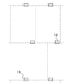
異なってしまう。このような状態を図17を用いて説明する。なお、図17は、各画素を
デルタ配置としたFFSモードの液晶表示パネル70Dの数画素分の概略平面図であって
、画素電極78Dとこの画素電極78Dに設けられたスリット77Dのみを示し、その他
の具体的構成は省略してある。また、図17における各画素間の破線は各画素の境界を示
し、実線は信号線の経路を示し、また、破線丸印で囲んだ部分はそれぞれの画素のTFT
が設けられている位置を示す。
In this case, in the FFS mode liquid crystal display panel, when each pixel has a delta arrangement, it is preferable that the shape of the slit is the same for all the pixel electrodes in order to reduce display unevenness. However, since it is necessary to arrange the signal lines with a short wiring length in a direction substantially perpendicular to the scanning lines although being in a crank shape, the positions of the TFTs are different between the odd rows and the even rows. Such a state will be described with reference to FIG. FIG. 17 is a schematic plan view of several pixels of an FFS mode liquid
Indicates the position where is provided.
図17に示したFFSモードの液晶表示パネル70Dは、奇数行の画素のTFTは図面上右下に位置するが、偶数行の画素のTFTは図面上左下に位置しているため、信号線をクランク状にではあるが縦方向に直線状にかつ配線長を短く配置することができる。しかしながら、このFFSモードの液晶表示パネル70Dは、奇数行の画素の画素電極に設けられたスリットの形状を表示開口を有効利用できるように最適な形状としたものであるが、偶数行の画素電極に設けられたスリットの形状は矢印Xで示す位置のスリットの形状が奇数行のものと異なってしまい、同じ形状にすることができないので、視角対称性が失われてしまう。そのため、このFFSモードの液晶表示パネル70Dを表示させた際には横方向に斑が生じてしまう。逆に各画素の画素電極のスリットの形状を奇数行と偶数行とで同一になるようにすると、表示開口を有効に利用することができなくなる。このような状況は、画素電極に設けるスリットをデュアルドメイン構造とした各画素をデルタ配置したFFSモードの液晶表示パネルについても同様に生じる現象である。
In the FFS mode liquid
本発明は、上述のような画素電極に設けるスリットをデュアルドメイン構造とした各画
素をデルタ配置したFFSモードの液晶表示パネルにおける問題点を解決すべくなされた
ものであって、視角対称性を有し、横方向の斑の発生がなく、しかも広視野角で、透過率
が高く明るい表示が可能で、表示画質が良好なFFSモードの液晶表示パネルを提供する
ことを目的とする。
The present invention has been made in order to solve the problems in the FFS mode liquid crystal display panel in which each pixel having a dual domain structure with slits provided in the pixel electrode as described above is provided, and has viewing angle symmetry. It is another object of the present invention to provide an FFS mode liquid crystal display panel which is free from horizontal spots, has a wide viewing angle, has a high transmittance, and can display bright images and has a good display image quality.
上記目的を達成するため、本願のFFSモードの液晶表示パネルの発明は、平行に設けられた複数の走査線と、前記走査線と直交する方向にクランク状に設けられた複数の信号線と、複数の前記走査線及び信号線の間にそれぞれ形成された画素電極とを有し、前記画素電極が、デルタ状に配置され、且つ前記信号線に対して互い違いの接続となるように形成されるフリンジ・フィールド・スィッチングモードの液晶表示パネルにおいて、前記複数の画素電極のそれぞれは隣り合う前記走査線の間に位置する前記走査線に平行な軸に対して互いに異なる方向に傾いた複数のスリットを有し、前記画素電極に形成されたスリットのパターンは奇数行の画素電極と偶数行の画素電極とで互いに左右反転した構造を備えていることを特徴とする。 In order to achieve the above object, the invention of the FFS mode liquid crystal display panel of the present application includes a plurality of scanning lines provided in parallel, and a plurality of signal lines provided in a crank shape in a direction perpendicular to the scanning lines, A plurality of pixel electrodes formed between the scanning lines and the signal lines, and the pixel electrodes are arranged in a delta shape and are alternately connected to the signal lines. In the fringe field switching mode liquid crystal display panel, each of the plurality of pixel electrodes has a plurality of slits inclined in different directions with respect to an axis parallel to the scanning line located between the adjacent scanning lines. And the slit pattern formed in the pixel electrode has a structure in which the odd-numbered pixel electrode and the even-numbered pixel electrode are reversed to each other .
また、本願のFFSモードの液晶表示パネルの発明は、上記FFSモードの液晶表示パ
ネルにおいて、前記走査線に平行な軸の両側に設けられたスリットの数はそれぞれの側で
同一数であることを特徴とする。
In the invention of the FFS mode liquid crystal display panel of the present application, in the FFS mode liquid crystal display panel, the number of slits provided on both sides of the axis parallel to the scanning line is the same on each side. Features.
また、本願のFFSモードの液晶表示パネルの発明は、上記FFSモードの液晶表示パネルにおいて、前記走査線に平行な軸と平面視で重なる領域の前記画素電極の下部には、コモン配線が設けられていることを特徴とする。 In the invention of the FFS mode liquid crystal display panel of the present application, in the FFS mode liquid crystal display panel, a common wiring is provided below the pixel electrode in a region overlapping with an axis parallel to the scanning line in plan view. It is characterized by.
また、本願のFFSモードの液晶表示パネルの発明は、上記FFSモードの液晶表示パ
ネルにおいて、前記走査線に平行な軸に最も近接する両側のスリットの端部は前記走査線
に平行な軸上で結合されていることを特徴とする。
Further, the invention of the FFS mode liquid crystal display panel of the present application is the above FFS mode liquid crystal display panel, wherein the ends of the slits on both sides closest to the axis parallel to the scanning line are on the axis parallel to the scanning line. It is characterized by being connected.
本発明は上記構成を備えることにより以下に述べるような優れた効果を奏する。すなわち、上記のFFSモードの液晶表示パネルの発明によれば、奇数行の画素と偶数行の画素とで画素電極を駆動するためのスイッチング素子、例えばTFTが異なる位置に存在することとなるが、信号線の配線長を短くできるとともに、しかも各画素の画素電極に設けられたスリットの形状は、デッドスペースを最小限にしながらも走査線に平行な軸に対して対称な実質的に同じ形状となっているとともに、行毎に走査線に垂直な軸に対して対称性を備えているから、表示開口を有効に利用しながら走査線に平行な方向及び垂直な方向ともに視角対称性が維持され、従来例のような横方向に斑が生じることがなくなるとともに明るい表示のFFSモードの液晶表示パネルが得られる。 By providing the above configuration, the present invention has the following excellent effects. That is, according to the above-described invention of the FFS mode liquid crystal display panel, the switching elements for driving the pixel electrodes, for example, the TFTs, are present at different positions in the odd row pixels and the even row pixels. The wiring length of the signal line can be shortened, and the shape of the slit provided in the pixel electrode of each pixel is substantially the same shape symmetrical with respect to the axis parallel to the scanning line while minimizing the dead space. Since each row has symmetry with respect to the axis perpendicular to the scanning line, viewing angle symmetry is maintained in both the direction parallel to and perpendicular to the scanning line while effectively using the display aperture. As a result, there are no spots in the horizontal direction as in the conventional example, and a bright display FFS mode liquid crystal display panel can be obtained.
また、上記発明によれば、走査線に平行な軸の両側に設けられた画素電極のスリットの
数はそれぞれの側で同一数とされているから、画素電極の形状は一画素内で走査線と平行
な軸に対して完全に近い対称性を有するようになり、走査線に垂直な方向の視角の対称性
が高まり、より広視野角で表示画質が良好なFFSモードの液晶表示パネルが得られる。
According to the above invention, the number of slits of the pixel electrode provided on both sides of the axis parallel to the scanning line is the same on each side, so the shape of the pixel electrode is within the scanning line within one pixel. As a result, the FFS mode liquid crystal display panel with a wider viewing angle and better display image quality can be obtained. It is done.
また、上記発明によれば、コモン配線は、通常は走査線と同材質の導電性材料から作製さ
れるために不透明であるが、このコモン配線によって互いに異なる方向に傾いたスリット
同士が隣り合う位置で発生するディスクリネーション部分を遮光することができ、表示画
質が良好なFFSモードの液晶表示パネルが得られる。
Further, according to the above invention, the common wiring is usually opaque because it is made of the same conductive material as the scanning line, but the slits inclined in different directions by the common wiring are adjacent to each other. Thus, an FFS mode liquid crystal display panel with good display image quality can be obtained.
上記発明によれば、走査線に平行な軸に最も近接する両側のスリットの端部を走査線に
平行な軸上で結合することによって、画素電極の面積を有効に利用することができ、しか
も両スリットの結合点近傍のディスクリネーションの発生が抑制されるため、表示画質が
より良好なFFSモードの液晶表示パネルが得られる。
According to the above invention, the area of the pixel electrode can be effectively utilized by coupling the ends of the slits on both sides closest to the axis parallel to the scanning line on the axis parallel to the scanning line, and Since the occurrence of disclination near the coupling point of both slits is suppressed, an FFS mode liquid crystal display panel with better display image quality can be obtained.
以下、図面を参照して本発明の最良の実施形態を説明する。但し、以下に示す実施形態
は、本発明の技術思想を具体化するためのFFSモードの液晶表示パネルの構成を製造工
程順に例示するものであって、本発明をこのFFSモードの液晶表示パネルに特定するこ
とを意図するものではなく、特許請求の範囲に含まれるその他の実施形態のものも等しく
適応し得るものである。
Hereinafter, the best embodiment of the present invention will be described with reference to the drawings. However, the embodiment described below exemplifies the configuration of the FFS mode liquid crystal display panel for embodying the technical idea of the present invention in the order of the manufacturing process, and the present invention is applied to the FFS mode liquid crystal display panel. It is not intended to be specific, and other embodiments within the scope of the claims are equally applicable.
なお、図1は走査線及びコモン配線形成工程で形成された走査線及びコモン配線のパタ
ーンを示す図であり、図2は対向電極形成工程で形成された対向電極のパターンを示す図
であり、図3は半導体層形成工程で形成された半導体層のパターンを示す図であり、図4
は信号線及びドレイン電極形成工程で形成された信号線及びドレイン電極のパターンを示
す図であり、図5はコンタクトホール形成工程で形成されたコンタクトホールのパターン
を示す図であり、図6は図1〜図5の全てパターンを上下関係を無視して重ねて表した平
面図である。
1 is a diagram showing a pattern of the scanning line and the common wiring formed in the scanning line and common wiring forming step, FIG. 2 is a diagram showing a pattern of the counter electrode formed in the counter electrode forming step, FIG. 3 is a diagram showing a pattern of the semiconductor layer formed in the semiconductor layer forming step.
FIG. 5 is a view showing a pattern of signal lines and drain electrodes formed in the signal line and drain electrode forming step, FIG. 5 is a view showing patterns of contact holes formed in the contact hole forming step, and FIG. FIG. 6 is a plan view showing all the patterns in FIGS.
更に、図7は画素電極形成工程で形成された画素電極のパターンを示す図であり、図8
は図6及び図7のパターンを上下関係を無視して重ねて表した平面図であり、図9はカラ
ーフィルタ基板に設けるブラックマトリクスのパターンを示す図であり、図10は図7の
パターンの上に図9のパターンを重ねて表した図である。
Further, FIG. 7 is a diagram showing a pattern of the pixel electrode formed in the pixel electrode forming step.
FIG. 9 is a plan view showing the patterns of FIG. 6 and FIG. 7 superimposed on each other ignoring the vertical relation, FIG. 9 is a diagram showing a pattern of a black matrix provided on the color filter substrate, and FIG. FIG. 10 is a diagram in which the pattern of FIG. 9 is overlaid on top.
この実施例のFFSモードの液晶表示パネル10の製造工程を、アレイ基板の製造工程
とカラーフィルタ基板の製造工程に分けて説明する。
[アレイ基板製造工程]
(1)走査線・コモン配線形成工程
まず、ガラス基板等の透明基板11の表面全体に亘って下部がAl金属からなり表面が
Mo金属からなる2層膜を形成した後、フォトリソグラフィー法及びエッチング法によっ
て、図1に示したようなパターンのそれぞれMo/Alの2層配線からなる複数の走査線
12及び複数のコモン配線13を互いに平行に形成する。その際、走査線12の一部にT
FTのゲート電極G部分を突出させておく。なお、コモン配線13は隣り合う走査線12
の中間に設けられる。なお、図1において破線部分は各画素の境界部分を示す(以下、他
の図面においても同じ。)
The manufacturing process of the FFS mode liquid
[Array substrate manufacturing process]
(1) Scanning line / common wiring formation step First, after forming a two-layer film having a lower part made of Al metal and a surface made of Mo metal over the entire surface of the
The gate electrode G portion of the FT is projected. The
It is provided in the middle. In FIG. 1, a broken line portion indicates a boundary portion of each pixel (hereinafter, the same applies to other drawings).
(2)対向電極形成工程
次いで、ITOからなる透明導電性層を(1)の走査線・コモン配線形成工程を経た透
明基板11の表面全体に亘って被覆し、同じくフォトリソグラフィー法及びエッチング法
によって、図2に示したようなパターンの対向電極15を形成する。この対向電極15は
コモン配線13とは電気的に接続されているが、走査線12ないしゲート電極Gとは接続
されていない。
(2) Counter electrode forming step Next, the transparent conductive layer made of ITO is covered over the entire surface of the
(3)絶縁膜形成工程
次いで、窒化硅素層ないしは酸化硅素層からなる絶縁膜を(2)の対向電極形成工程を
経た透明基板11の表面全体に亘って被覆する。
(3) Insulating Film Forming Step Next, an insulating film made of a silicon nitride layer or a silicon oxide layer is coated over the entire surface of the
(4)半導体層形成工程
次いで、CVD法によりアモルファス・シリコン(以下「a−Si」という。)層を(
3)の絶縁膜形成工程を経た透明基板11の表面全体に亘って被覆し、同じくフォトリソ
グラフィー法及びエッチング法によって、図3に示したようなパターンのa−Si層から
なる半導体層19をゲート電極G上に位置するように形成する。
(4) Semiconductor Layer Formation Step Next, an amorphous silicon (hereinafter referred to as “a-Si”) layer is formed by CVD (
3) Covers the entire surface of the
(5)信号線・ドレイン電極形成工程
次いで、Mo/Al/Moの3層構造の導電性層を(4)の半導体層形成工程を経た透
明基板11の表面全体に亘って被覆し、同じくフォトリソグラフィー法及びエッチング法
によって、図4に示したようなパターンの信号線14及びドレイン電極Dを形成する。こ
の信号線14のソース電極S部分及びドレイン電極D部分は、いずれも半導体層19の表
面に部分的に重なっている。
(5) Signal Line / Drain Electrode Formation Step Next, a conductive layer having a three-layer structure of Mo / Al / Mo is coated over the entire surface of the
(6)パッシベーション膜形成工程
次いで、窒化硅素層からなるパッシベーション膜を(5)の信号線・ドレイン電極形成
工程を経た透明基板11の表面全体に被覆する。
(6) Passivation Film Formation Step Next, the entire surface of the
(7)コンタクトホール形成工程
次いで、(6)のパッシベーション膜形成工程を経た透明基板11に対し、同じくフォ
トリソグラフィー法及びエッチング法によって、パッシベーション膜の所定位置にコンタ
クトホール20を形成し、ドレイン電極Dの一部を露出させる。このコンタクトホール形
成工程を経た透明基板11の平面図を、各層の上下関係を無視して透視して表すと図6に
示したとおりとなる。
(7) Contact hole forming step Next, a
(8)画素電極形成工程
更に、ITOからなる透明導電性層を(7)のコンタクトホール形成工程を経た透明基
板11の表面全体に亘って被覆し、同じくフォトリソグラフィー法及びエッチング法によ
って、図7に示したパターンとなるようにスリット171を有する奇数行の画素電極18
1及びスリット172を有する偶数行の画素電極182を形成する。この画素電極181
及び182はともにコンタクトホール20を介してドレイン電極Dと電気的に接続されて
いる。この画素電極形成工程を経た透明基板11の平面図を、各層の上下関係を無視して
透視して表すと図8に示したとおりとなる。この後、表面全体に所定の配向膜(図示せず
)を形成することによりアレイ基板ARが完成される。なお、画素電極181及び182
に設けるそれぞれのスリット171及び172の形状等については後述する。
(8) Pixel Electrode Formation Step Further, a transparent conductive layer made of ITO is coated over the entire surface of the
1 and a pixel electrode 18 2 of the even rows with
And 18 2 are connected together the
It will be described later for each of the
[カラーフィルタ基板製造工程]
カラーフィルタ基板は、図示しないガラス基板等からなる透明基板の表面全体に例えば
感光性樹脂からなるブラックマトリクス形成材料の層を設け、フォトリソグラフィー法に
より図9に示すようなパターンのブラックマトリクス21を形成し、次いで、各画素に対
応する位置にそれぞれ例えばRGBの3原色のカラーフィルタ層を形成し、次いで、カラ
ーフィルタ層の表面に表面が平らになるようにオーバーコート層を形成する。更に、オー
バーコート層の表面に所定の配向膜を形成するとともに所定位置にスペーサを形成するこ
とによりカラーフィルタ基板が完成される。
[Color filter substrate manufacturing process]
For the color filter substrate, a black matrix forming material layer made of, for example, a photosensitive resin is provided on the entire surface of a transparent substrate made of a glass substrate (not shown), and a
その後、アレイ基板AR及びカラーフィルタ基板を対向させ、周囲をシール材でシール
して両基板間に液晶を注入することにより実施例に係るFFSモードの液晶表示パネル1
0が得られる。なお、この実施例に係るFFSモードの液晶表示パネル10の画素電極1
81及び182とブラックマトリクス21との配置関係は、ブラックマトリクス21側か
ら見ると図10に示したとおりとなる、
Thereafter, the array substrate AR and the color filter substrate are made to face each other, the periphery is sealed with a sealing material, and liquid crystal is injected between both the substrates, whereby the FFS mode liquid
0 is obtained. The
The arrangement relationship between 8 1 and 18 2 and the
以下では、この実施例に係るFFSモードの液晶表示パネル10の画素電極181及び
182に設けるそれぞれのスリット171及び172の形状について図7、図8及び図1
0を参照しながら説明する。奇数行の画素電極181に設けられた複数のスリット171
は、隣り合う走査線12の間に位置するコモン配線13が設けられている箇所に該当する
走査線12に平行な軸x(図7及び図8参照)に対して左上側及び左下側に傾いた状態に
、実質的に軸xに対して線対称となるように、同一の本数ずつ設けられている。同様に、
偶数行の画素電極182に設けられた複数のスリット172は、軸xに対して右上側及び
右下側に傾いた状態に、実質的に軸xに対して線対称となるように、同一の本数ずつ設け
られている。従って、この実施例に係るFFSモードの液晶表示パネル10における全て
の画素の画素電極は、画素電極単位で走査線12に平行な軸xに対して対称性を備えてい
るため、走査線12に直交する方向には表示画質に視角依存性が少なくなる。なお、軸x
の両側に設けられるスリットの本数は、互いに異なっていてもよいが、あえて異なるよう
にすることの利点はないので、視角対称性を確保するために同一の本数ずつ設けることが
好ましい。
Hereinafter, the shapes of the
This will be described with reference to 0. A plurality of
Is inclined to the upper left side and the lower left side with respect to an axis x (see FIGS. 7 and 8) parallel to the
A plurality of
The number of slits provided on both sides may be different from each other, but since there is no advantage of making it different, it is preferable to provide the same number of slits in order to ensure viewing angle symmetry.
加えて、この実施例に係るFFSモードの液晶表示パネル10においては、奇数行の画素電極181に設けられた複数のスリット171と偶数行の画素電極182に設けられた複数のスリット172とは走査線12に垂直な軸に対して互いに反転した構成となっている。このことは、奇数行の画素電極181の製造用マスクを反転(裏返す)させて使用することにより偶数行の画素電極182を製造できることを意味する。従って、この実施例に係るFFSモードの液晶表示パネル10においては行毎に走査線に垂直な軸に対して対称性を備えているから、走査線12に沿った方向においても表示画質に視角依存性が少なくなる。このように、実施例に係るFFSモードの液晶表示パネル10においては、表示開口を有効に利用しながら走査線に垂直な方向及び走査線に沿った方向ともに視角対称性が維持され、従来例のような横方向に斑が生じることがなくなるとともに明るい表示のFFSモードの液晶表示パネルが得られる。
In addition, in the FFS mode liquid
また、実施例に係るFFSモードの液晶表示パネル10においては、コモン配線13は
走査線12と同材質のMo/Alの2層配線からなるため、遮光性である。そして走査線
12に平行な軸xに最も近接する両側のスリットの端部は、軸x上で、すなわちコモン配
線13の上部で結合されて「く」字状とされている。この走査線12に平行な軸xに最も
近接する両側のスリットは、それぞれ傾斜方向が異なるために軸xを起点として液晶分子
の配向方向が異なる状態となるので、軸xに沿ってディスクリネーションが発生するが、
このディクリネーション発生部分はコモン配線13によって遮光されている。そのため、
発生したディスクリネーションは外部から視認し難くなるため、表示画質が向上する。
Further, in the FFS mode liquid
This declination occurrence portion is shielded from light by the
The generated disclination becomes difficult to visually recognize from the outside, so that the display image quality is improved.
10 FFSモードの液晶表示パネル
11 透明基板
12 走査線
13 コモン配線
14 信号線
15 対向電極
171、172 スリット
181、182 画素電極
19 半導体層
20 コンタクトホール
21 ブラックマトリクス
x 走査線に平行な軸
10 FFS mode liquid
Claims (4)
Priority Applications (5)
| Application Number | Priority Date | Filing Date | Title |
|---|---|---|---|
| JP2006088208A JP4238877B2 (en) | 2006-03-28 | 2006-03-28 | FFS mode LCD panel |
| KR1020070022602A KR100853070B1 (en) | 2006-03-28 | 2007-03-07 | Ffs mode liquid crystal display panel |
| US11/727,005 US8711311B2 (en) | 2006-03-28 | 2007-03-23 | Fringe field switching mode liquid crystal display panel |
| TW096110440A TWI365315B (en) | 2006-03-28 | 2007-03-27 | Ffs mode liquid crystal display panel |
| CN2007100909758A CN101046592B (en) | 2006-03-28 | 2007-03-28 | FFS mode liquid crystal display panel |
Applications Claiming Priority (1)
| Application Number | Priority Date | Filing Date | Title |
|---|---|---|---|
| JP2006088208A JP4238877B2 (en) | 2006-03-28 | 2006-03-28 | FFS mode LCD panel |
Publications (3)
| Publication Number | Publication Date |
|---|---|
| JP2007264231A JP2007264231A (en) | 2007-10-11 |
| JP2007264231A5 JP2007264231A5 (en) | 2008-05-15 |
| JP4238877B2 true JP4238877B2 (en) | 2009-03-18 |
Family
ID=38558351
Family Applications (1)
| Application Number | Title | Priority Date | Filing Date |
|---|---|---|---|
| JP2006088208A Expired - Fee Related JP4238877B2 (en) | 2006-03-28 | 2006-03-28 | FFS mode LCD panel |
Country Status (5)
| Country | Link |
|---|---|
| US (1) | US8711311B2 (en) |
| JP (1) | JP4238877B2 (en) |
| KR (1) | KR100853070B1 (en) |
| CN (1) | CN101046592B (en) |
| TW (1) | TWI365315B (en) |
Cited By (4)
| Publication number | Priority date | Publication date | Assignee | Title |
|---|---|---|---|---|
| KR20130084623A (en) | 2012-01-17 | 2013-07-25 | 스탄레 덴끼 가부시키가이샤 | Liquid crystal device and drive method thereof |
| US9348191B2 (en) | 2012-12-06 | 2016-05-24 | Stanley Electric Co., Ltd. | Liquid crystal element and liquid crystal display apparatus |
| US9354481B2 (en) | 2013-08-21 | 2016-05-31 | Stanley Electric Co., Ltd. | Liquid crystal element and liquid crystal display apparatus |
| US11789323B2 (en) | 2019-09-25 | 2023-10-17 | Toppan Inc. | Liquid crystal display device |
Families Citing this family (40)
| Publication number | Priority date | Publication date | Assignee | Title |
|---|---|---|---|---|
| KR100632632B1 (en) | 2004-05-28 | 2006-10-12 | 삼성전자주식회사 | Method for preparing a multi-layer of nano-crystals and organic-inorganic hybrid electro-luminescence device using the same |
| JP4475303B2 (en) * | 2007-08-17 | 2010-06-09 | ソニー株式会社 | Display device |
| JP5072530B2 (en) * | 2007-10-23 | 2012-11-14 | 株式会社ジャパンディスプレイウェスト | Liquid crystal device and electronic device including the same |
| JP4609483B2 (en) * | 2007-11-21 | 2011-01-12 | ソニー株式会社 | Liquid crystal display device |
| JP4600463B2 (en) * | 2007-11-21 | 2010-12-15 | ソニー株式会社 | Liquid crystal display |
| JP5202938B2 (en) * | 2007-12-21 | 2013-06-05 | 株式会社ジャパンディスプレイウェスト | Liquid crystal display |
| EP2077466A1 (en) * | 2008-01-07 | 2009-07-08 | TPO Displays Corp. | Electrode structure for an LCD device |
| JP5143583B2 (en) * | 2008-02-08 | 2013-02-13 | 株式会社ジャパンディスプレイウェスト | LCD panel |
| JP2009198703A (en) | 2008-02-20 | 2009-09-03 | Sony Corp | Liquid crystal display device and method of manufacturing the same |
| JP5243060B2 (en) * | 2008-02-21 | 2013-07-24 | 株式会社ジャパンディスプレイウェスト | Liquid crystal display |
| JP5246782B2 (en) | 2008-03-06 | 2013-07-24 | 株式会社ジャパンディスプレイウェスト | Liquid crystal device and electronic device |
| JP5121529B2 (en) | 2008-03-27 | 2013-01-16 | 株式会社ジャパンディスプレイウェスト | Liquid crystal display device and electronic device |
| JP5175127B2 (en) * | 2008-03-28 | 2013-04-03 | 株式会社ジャパンディスプレイウェスト | Liquid crystal display |
| JP5137680B2 (en) * | 2008-05-08 | 2013-02-06 | 株式会社ジャパンディスプレイウェスト | Liquid crystal display |
| JP5224973B2 (en) * | 2008-08-26 | 2013-07-03 | 株式会社ジャパンディスプレイウェスト | Information input / output device and information input / output method |
| KR101323391B1 (en) * | 2008-12-12 | 2013-10-29 | 엘지디스플레이 주식회사 | Liquid Crystal Display |
| US20100208179A1 (en) * | 2009-02-13 | 2010-08-19 | Apple Inc. | Pixel Black Mask Design and Formation Technique |
| US8294647B2 (en) * | 2009-02-13 | 2012-10-23 | Apple Inc. | LCD pixel design varying by color |
| US8558978B2 (en) * | 2009-02-13 | 2013-10-15 | Apple Inc. | LCD panel with index-matching passivation layers |
| US8587758B2 (en) * | 2009-02-13 | 2013-11-19 | Apple Inc. | Electrodes for use in displays |
| US8345177B2 (en) * | 2009-02-13 | 2013-01-01 | Shih Chang Chang | Via design for use in displays |
| US8390553B2 (en) * | 2009-02-13 | 2013-03-05 | Apple Inc. | Advanced pixel design for optimized driving |
| US8633879B2 (en) | 2009-02-13 | 2014-01-21 | Apple Inc. | Undulating electrodes for improved viewing angle and color shift |
| US9612489B2 (en) * | 2009-02-13 | 2017-04-04 | Apple Inc. | Placement and shape of electrodes for use in displays |
| US8531408B2 (en) * | 2009-02-13 | 2013-09-10 | Apple Inc. | Pseudo multi-domain design for improved viewing angle and color shift |
| US8111232B2 (en) | 2009-03-27 | 2012-02-07 | Apple Inc. | LCD electrode arrangement |
| US8294850B2 (en) | 2009-03-31 | 2012-10-23 | Apple Inc. | LCD panel having improved response |
| TW201118491A (en) * | 2009-11-27 | 2011-06-01 | Au Optronics Corp | Display panel |
| JP5466973B2 (en) * | 2010-03-04 | 2014-04-09 | 株式会社ジャパンディスプレイ | Liquid crystal display |
| KR20120004045A (en) | 2010-07-06 | 2012-01-12 | 삼성전자주식회사 | Liquid crystal display |
| JP5551553B2 (en) * | 2010-09-29 | 2014-07-16 | 株式会社ジャパンディスプレイ | Liquid crystal display |
| WO2012050053A1 (en) * | 2010-10-15 | 2012-04-19 | シャープ株式会社 | Liquid crystal display device |
| US8953134B2 (en) | 2011-01-20 | 2015-02-10 | Japan Display West Inc. | Liquid crystal display panel |
| US8531635B2 (en) | 2011-04-12 | 2013-09-10 | Japan Display West Inc. | Liquid-crystal display apparatus |
| JP5750074B2 (en) * | 2012-03-12 | 2015-07-15 | 株式会社ジャパンディスプレイ | Liquid crystal display device, method for manufacturing liquid crystal display device, and electronic apparatus |
| KR102353725B1 (en) | 2015-05-27 | 2022-01-20 | 삼성디스플레이 주식회사 | Liquid crystal display |
| DE102015113183B4 (en) | 2015-08-10 | 2018-06-28 | Yuan-Hung WEN | Cable operated drive assembly for vehicles |
| DE102015017184B4 (en) | 2015-08-10 | 2020-02-13 | Yuan-Hung WEN | Cable drive assembly for vehicles |
| CN107589585A (en) * | 2017-09-22 | 2018-01-16 | 惠科股份有限公司 | Liquid crystal display panel |
| CN108287442B (en) * | 2018-02-06 | 2021-11-16 | 重庆京东方光电科技有限公司 | Array substrate repairing method and array substrate |
Family Cites Families (16)
| Publication number | Priority date | Publication date | Assignee | Title |
|---|---|---|---|---|
| JP3464570B2 (en) * | 1995-08-21 | 2003-11-10 | 株式会社 日立ディスプレイズ | Color liquid crystal display device |
| JP3036512B2 (en) | 1998-05-26 | 2000-04-24 | 日本電気株式会社 | Liquid crystal display |
| KR20000027776A (en) | 1998-10-29 | 2000-05-15 | 김영환 | Method for manufacturing lcd |
| KR100520381B1 (en) | 2000-05-31 | 2005-10-11 | 비오이 하이디스 테크놀로지 주식회사 | Fringe field switching mode lcd device |
| KR20020010209A (en) | 2000-07-27 | 2002-02-04 | 윤종용 | a structure of a pixel array and a panel for a liquid crystal display including the same |
| KR100482468B1 (en) * | 2000-10-10 | 2005-04-14 | 비오이 하이디스 테크놀로지 주식회사 | Fringe field switching mode lcd |
| KR100713882B1 (en) | 2000-12-01 | 2007-05-07 | 비오이 하이디스 테크놀로지 주식회사 | FFS mode thin film transistor liquid crystal display |
| KR100471397B1 (en) * | 2001-05-31 | 2005-02-21 | 비오이 하이디스 테크놀로지 주식회사 | Apparatus for fringe field switching liquid crystal display and method for manufacturing the same |
| JP4373052B2 (en) | 2002-05-06 | 2009-11-25 | 大林精工株式会社 | Ultra high aperture ratio wide viewing angle LCD |
| KR100852807B1 (en) | 2002-07-29 | 2008-08-18 | 비오이 하이디스 테크놀로지 주식회사 | fringe field switching mode liquid crystal display |
| KR20050004410A (en) * | 2003-07-02 | 2005-01-12 | 삼성전자주식회사 | Color filter panel and liquid crystal display including the same |
| JP4163611B2 (en) | 2003-12-26 | 2008-10-08 | 株式会社 日立ディスプレイズ | Liquid crystal display |
| JP4223992B2 (en) | 2004-05-25 | 2009-02-12 | 株式会社 日立ディスプレイズ | Liquid crystal display |
| KR101050348B1 (en) * | 2004-05-31 | 2011-07-19 | 엘지디스플레이 주식회사 | Transverse electric field liquid crystal display device |
| US7557886B2 (en) * | 2004-06-29 | 2009-07-07 | Lg Display Co., Ltd. | Liquid crystal display device and method of fabricating the same |
| KR20070001652A (en) * | 2005-06-29 | 2007-01-04 | 엘지.필립스 엘시디 주식회사 | Fringe field switching mode liquid crystal display device |
-
2006
- 2006-03-28 JP JP2006088208A patent/JP4238877B2/en not_active Expired - Fee Related
-
2007
- 2007-03-07 KR KR1020070022602A patent/KR100853070B1/en active IP Right Grant
- 2007-03-23 US US11/727,005 patent/US8711311B2/en active Active
- 2007-03-27 TW TW096110440A patent/TWI365315B/en not_active IP Right Cessation
- 2007-03-28 CN CN2007100909758A patent/CN101046592B/en active Active
Cited By (5)
| Publication number | Priority date | Publication date | Assignee | Title |
|---|---|---|---|---|
| KR20130084623A (en) | 2012-01-17 | 2013-07-25 | 스탄레 덴끼 가부시키가이샤 | Liquid crystal device and drive method thereof |
| KR20190004685A (en) | 2012-01-17 | 2019-01-14 | 스탄레 덴끼 가부시키가이샤 | Liquid crystal device and Liquid crystal display device |
| US9348191B2 (en) | 2012-12-06 | 2016-05-24 | Stanley Electric Co., Ltd. | Liquid crystal element and liquid crystal display apparatus |
| US9354481B2 (en) | 2013-08-21 | 2016-05-31 | Stanley Electric Co., Ltd. | Liquid crystal element and liquid crystal display apparatus |
| US11789323B2 (en) | 2019-09-25 | 2023-10-17 | Toppan Inc. | Liquid crystal display device |
Also Published As
| Publication number | Publication date |
|---|---|
| US20070229749A1 (en) | 2007-10-04 |
| CN101046592A (en) | 2007-10-03 |
| KR20070097308A (en) | 2007-10-04 |
| CN101046592B (en) | 2012-05-23 |
| JP2007264231A (en) | 2007-10-11 |
| KR100853070B1 (en) | 2008-08-19 |
| TWI365315B (en) | 2012-06-01 |
| US8711311B2 (en) | 2014-04-29 |
| TW200745666A (en) | 2007-12-16 |
Similar Documents
| Publication | Publication Date | Title |
|---|---|---|
| JP4238877B2 (en) | FFS mode LCD panel | |
| JP4201051B2 (en) | LCD panel | |
| US11774809B2 (en) | Liquid crystal display panel | |
| JP5246782B2 (en) | Liquid crystal device and electronic device | |
| US9176339B2 (en) | Liquid crystal display device | |
| US7787091B2 (en) | Transverse field type liquid crystal display panel | |
| JP5875001B2 (en) | Horizontal electric field type liquid crystal display device | |
| US8724064B2 (en) | Fringe field switching mode liquid crystal display device and method of fabricating the same | |
| KR20020041426A (en) | Liquid crystal display | |
| JP4386102B2 (en) | Horizontal electric field LCD panel | |
| US20050128406A1 (en) | In-plane switching mode liquid crystal display device and method of fabricating the same | |
| US20170153482A1 (en) | Liquid crystal display device | |
| JP2013190703A (en) | Liquid crystal display device | |
| JP4449958B2 (en) | FFS liquid crystal display panel | |
| JP4407677B2 (en) | Horizontal electric field LCD panel | |
| JP5067756B2 (en) | LCD panel | |
| KR20040100903A (en) | Electro-optical device, electronic apparatus, and projection display apparatus | |
| JP5271021B2 (en) | Liquid crystal display | |
| JP5660765B2 (en) | LCD panel | |
| JP2009069332A (en) | Liquid crystal display panel | |
| JP2008065212A (en) | Liquid crystal display panel | |
| JP2008051846A (en) | Liquid crystal display panel of fringe field switching (ffs) mode | |
| JP2008134498A (en) | Liquid crystal display panel and method for manufacturing the same | |
| KR20050059398A (en) | Fringe field switching mode liquid crystal display device and method for manufacturing the same |
Legal Events
| Date | Code | Title | Description |
|---|---|---|---|
| A621 | Written request for application examination |
Free format text: JAPANESE INTERMEDIATE CODE: A621 Effective date: 20080107 |
|
| A521 | Written amendment |
Free format text: JAPANESE INTERMEDIATE CODE: A523 Effective date: 20080402 |
|
| A871 | Explanation of circumstances concerning accelerated examination |
Free format text: JAPANESE INTERMEDIATE CODE: A871 Effective date: 20080402 |
|
| A975 | Report on accelerated examination |
Free format text: JAPANESE INTERMEDIATE CODE: A971005 Effective date: 20080501 |
|
| A131 | Notification of reasons for refusal |
Free format text: JAPANESE INTERMEDIATE CODE: A131 Effective date: 20080507 |
|
| TRDD | Decision of grant or rejection written | ||
| A01 | Written decision to grant a patent or to grant a registration (utility model) |
Free format text: JAPANESE INTERMEDIATE CODE: A01 Effective date: 20081125 |
|
| A01 | Written decision to grant a patent or to grant a registration (utility model) |
Free format text: JAPANESE INTERMEDIATE CODE: A01 |
|
| A61 | First payment of annual fees (during grant procedure) |
Free format text: JAPANESE INTERMEDIATE CODE: A61 Effective date: 20081208 |
|
| FPAY | Renewal fee payment (event date is renewal date of database) |
Free format text: PAYMENT UNTIL: 20120109 Year of fee payment: 3 |
|
| R150 | Certificate of patent or registration of utility model |
Ref document number: 4238877 Country of ref document: JP Free format text: JAPANESE INTERMEDIATE CODE: R150 Free format text: JAPANESE INTERMEDIATE CODE: R150 |
|
| FPAY | Renewal fee payment (event date is renewal date of database) |
Free format text: PAYMENT UNTIL: 20120109 Year of fee payment: 3 |
|
| S111 | Request for change of ownership or part of ownership |
Free format text: JAPANESE INTERMEDIATE CODE: R313113 |
|
| FPAY | Renewal fee payment (event date is renewal date of database) |
Free format text: PAYMENT UNTIL: 20120109 Year of fee payment: 3 |
|
| R360 | Written notification for declining of transfer of rights |
Free format text: JAPANESE INTERMEDIATE CODE: R360 |
|
| FPAY | Renewal fee payment (event date is renewal date of database) |
Free format text: PAYMENT UNTIL: 20120109 Year of fee payment: 3 |
|
| S111 | Request for change of ownership or part of ownership |
Free format text: JAPANESE INTERMEDIATE CODE: R313113 |
|
| FPAY | Renewal fee payment (event date is renewal date of database) |
Free format text: PAYMENT UNTIL: 20120109 Year of fee payment: 3 |
|
| R350 | Written notification of registration of transfer |
Free format text: JAPANESE INTERMEDIATE CODE: R350 |
|
| FPAY | Renewal fee payment (event date is renewal date of database) |
Free format text: PAYMENT UNTIL: 20120109 Year of fee payment: 3 |
|
| FPAY | Renewal fee payment (event date is renewal date of database) |
Free format text: PAYMENT UNTIL: 20130109 Year of fee payment: 4 |
|
| R250 | Receipt of annual fees |
Free format text: JAPANESE INTERMEDIATE CODE: R250 |
|
| FPAY | Renewal fee payment (event date is renewal date of database) |
Free format text: PAYMENT UNTIL: 20130109 Year of fee payment: 4 |
|
| S111 | Request for change of ownership or part of ownership |
Free format text: JAPANESE INTERMEDIATE CODE: R313113 |
|
| FPAY | Renewal fee payment (event date is renewal date of database) |
Free format text: PAYMENT UNTIL: 20130109 Year of fee payment: 4 |
|
| R350 | Written notification of registration of transfer |
Free format text: JAPANESE INTERMEDIATE CODE: R350 |
|
| FPAY | Renewal fee payment (event date is renewal date of database) |
Free format text: PAYMENT UNTIL: 20140109 Year of fee payment: 5 |
|
| R250 | Receipt of annual fees |
Free format text: JAPANESE INTERMEDIATE CODE: R250 |
|
| R250 | Receipt of annual fees |
Free format text: JAPANESE INTERMEDIATE CODE: R250 |
|
| R250 | Receipt of annual fees |
Free format text: JAPANESE INTERMEDIATE CODE: R250 |
|
| R250 | Receipt of annual fees |
Free format text: JAPANESE INTERMEDIATE CODE: R250 |
|
| R250 | Receipt of annual fees |
Free format text: JAPANESE INTERMEDIATE CODE: R250 |
|
| R250 | Receipt of annual fees |
Free format text: JAPANESE INTERMEDIATE CODE: R250 |
|
| R250 | Receipt of annual fees |
Free format text: JAPANESE INTERMEDIATE CODE: R250 |
|
| LAPS | Cancellation because of no payment of annual fees |