JP4212293B2 - Manufacturing method of semiconductor device - Google Patents
Manufacturing method of semiconductor device Download PDFInfo
- Publication number
- JP4212293B2 JP4212293B2 JP2002111571A JP2002111571A JP4212293B2 JP 4212293 B2 JP4212293 B2 JP 4212293B2 JP 2002111571 A JP2002111571 A JP 2002111571A JP 2002111571 A JP2002111571 A JP 2002111571A JP 4212293 B2 JP4212293 B2 JP 4212293B2
- Authority
- JP
- Japan
- Prior art keywords
- film
- semiconductor device
- manufacturing
- semiconductor wafer
- support
- Prior art date
- Legal status (The legal status is an assumption and is not a legal conclusion. Google has not performed a legal analysis and makes no representation as to the accuracy of the status listed.)
- Expired - Fee Related
Links
Images


Classifications
-
- H—ELECTRICITY
- H01—ELECTRIC ELEMENTS
- H01L—SEMICONDUCTOR DEVICES NOT COVERED BY CLASS H10
- H01L24/00—Arrangements for connecting or disconnecting semiconductor or solid-state bodies; Methods or apparatus related thereto
- H01L24/01—Means for bonding being attached to, or being formed on, the surface to be connected, e.g. chip-to-package, die-attach, "first-level" interconnects; Manufacturing methods related thereto
- H01L24/02—Bonding areas ; Manufacturing methods related thereto
- H01L24/03—Manufacturing methods
-
- H—ELECTRICITY
- H01—ELECTRIC ELEMENTS
- H01L—SEMICONDUCTOR DEVICES NOT COVERED BY CLASS H10
- H01L2224/00—Indexing scheme for arrangements for connecting or disconnecting semiconductor or solid-state bodies and methods related thereto as covered by H01L24/00
- H01L2224/01—Means for bonding being attached to, or being formed on, the surface to be connected, e.g. chip-to-package, die-attach, "first-level" interconnects; Manufacturing methods related thereto
- H01L2224/02—Bonding areas; Manufacturing methods related thereto
- H01L2224/03—Manufacturing methods
- H01L2224/03001—Involving a temporary auxiliary member not forming part of the manufacturing apparatus, e.g. removable or sacrificial coating, film or substrate
- H01L2224/03002—Involving a temporary auxiliary member not forming part of the manufacturing apparatus, e.g. removable or sacrificial coating, film or substrate for supporting the semiconductor or solid-state body
-
- H—ELECTRICITY
- H01—ELECTRIC ELEMENTS
- H01L—SEMICONDUCTOR DEVICES NOT COVERED BY CLASS H10
- H01L2224/00—Indexing scheme for arrangements for connecting or disconnecting semiconductor or solid-state bodies and methods related thereto as covered by H01L24/00
- H01L2224/01—Means for bonding being attached to, or being formed on, the surface to be connected, e.g. chip-to-package, die-attach, "first-level" interconnects; Manufacturing methods related thereto
- H01L2224/02—Bonding areas; Manufacturing methods related thereto
- H01L2224/04—Structure, shape, material or disposition of the bonding areas prior to the connecting process
- H01L2224/0401—Bonding areas specifically adapted for bump connectors, e.g. under bump metallisation [UBM]
-
- H—ELECTRICITY
- H01—ELECTRIC ELEMENTS
- H01L—SEMICONDUCTOR DEVICES NOT COVERED BY CLASS H10
- H01L2224/00—Indexing scheme for arrangements for connecting or disconnecting semiconductor or solid-state bodies and methods related thereto as covered by H01L24/00
- H01L2224/01—Means for bonding being attached to, or being formed on, the surface to be connected, e.g. chip-to-package, die-attach, "first-level" interconnects; Manufacturing methods related thereto
- H01L2224/02—Bonding areas; Manufacturing methods related thereto
- H01L2224/04—Structure, shape, material or disposition of the bonding areas prior to the connecting process
- H01L2224/05—Structure, shape, material or disposition of the bonding areas prior to the connecting process of an individual bonding area
- H01L2224/05001—Internal layers
- H01L2224/0502—Disposition
- H01L2224/05025—Disposition the internal layer being disposed on a via connection of the semiconductor or solid-state body
-
- H—ELECTRICITY
- H01—ELECTRIC ELEMENTS
- H01L—SEMICONDUCTOR DEVICES NOT COVERED BY CLASS H10
- H01L2224/00—Indexing scheme for arrangements for connecting or disconnecting semiconductor or solid-state bodies and methods related thereto as covered by H01L24/00
- H01L2224/01—Means for bonding being attached to, or being formed on, the surface to be connected, e.g. chip-to-package, die-attach, "first-level" interconnects; Manufacturing methods related thereto
- H01L2224/02—Bonding areas; Manufacturing methods related thereto
- H01L2224/04—Structure, shape, material or disposition of the bonding areas prior to the connecting process
- H01L2224/05—Structure, shape, material or disposition of the bonding areas prior to the connecting process of an individual bonding area
- H01L2224/0554—External layer
- H01L2224/05541—Structure
- H01L2224/05548—Bonding area integrally formed with a redistribution layer on the semiconductor or solid-state body
-
- H—ELECTRICITY
- H01—ELECTRIC ELEMENTS
- H01L—SEMICONDUCTOR DEVICES NOT COVERED BY CLASS H10
- H01L2224/00—Indexing scheme for arrangements for connecting or disconnecting semiconductor or solid-state bodies and methods related thereto as covered by H01L24/00
- H01L2224/01—Means for bonding being attached to, or being formed on, the surface to be connected, e.g. chip-to-package, die-attach, "first-level" interconnects; Manufacturing methods related thereto
- H01L2224/02—Bonding areas; Manufacturing methods related thereto
- H01L2224/04—Structure, shape, material or disposition of the bonding areas prior to the connecting process
- H01L2224/05—Structure, shape, material or disposition of the bonding areas prior to the connecting process of an individual bonding area
- H01L2224/0554—External layer
- H01L2224/0556—Disposition
- H01L2224/0557—Disposition the external layer being disposed on a via connection of the semiconductor or solid-state body
-
- H—ELECTRICITY
- H01—ELECTRIC ELEMENTS
- H01L—SEMICONDUCTOR DEVICES NOT COVERED BY CLASS H10
- H01L2224/00—Indexing scheme for arrangements for connecting or disconnecting semiconductor or solid-state bodies and methods related thereto as covered by H01L24/00
- H01L2224/01—Means for bonding being attached to, or being formed on, the surface to be connected, e.g. chip-to-package, die-attach, "first-level" interconnects; Manufacturing methods related thereto
- H01L2224/02—Bonding areas; Manufacturing methods related thereto
- H01L2224/04—Structure, shape, material or disposition of the bonding areas prior to the connecting process
- H01L2224/06—Structure, shape, material or disposition of the bonding areas prior to the connecting process of a plurality of bonding areas
- H01L2224/061—Disposition
- H01L2224/0618—Disposition being disposed on at least two different sides of the body, e.g. dual array
- H01L2224/06181—On opposite sides of the body
-
- H—ELECTRICITY
- H01—ELECTRIC ELEMENTS
- H01L—SEMICONDUCTOR DEVICES NOT COVERED BY CLASS H10
- H01L2224/00—Indexing scheme for arrangements for connecting or disconnecting semiconductor or solid-state bodies and methods related thereto as covered by H01L24/00
- H01L2224/01—Means for bonding being attached to, or being formed on, the surface to be connected, e.g. chip-to-package, die-attach, "first-level" interconnects; Manufacturing methods related thereto
- H01L2224/10—Bump connectors; Manufacturing methods related thereto
- H01L2224/11—Manufacturing methods
- H01L2224/11001—Involving a temporary auxiliary member not forming part of the manufacturing apparatus, e.g. removable or sacrificial coating, film or substrate
- H01L2224/11002—Involving a temporary auxiliary member not forming part of the manufacturing apparatus, e.g. removable or sacrificial coating, film or substrate for supporting the semiconductor or solid-state body
-
- H—ELECTRICITY
- H01—ELECTRIC ELEMENTS
- H01L—SEMICONDUCTOR DEVICES NOT COVERED BY CLASS H10
- H01L2224/00—Indexing scheme for arrangements for connecting or disconnecting semiconductor or solid-state bodies and methods related thereto as covered by H01L24/00
- H01L2224/01—Means for bonding being attached to, or being formed on, the surface to be connected, e.g. chip-to-package, die-attach, "first-level" interconnects; Manufacturing methods related thereto
- H01L2224/10—Bump connectors; Manufacturing methods related thereto
- H01L2224/12—Structure, shape, material or disposition of the bump connectors prior to the connecting process
- H01L2224/13—Structure, shape, material or disposition of the bump connectors prior to the connecting process of an individual bump connector
- H01L2224/13001—Core members of the bump connector
- H01L2224/1302—Disposition
- H01L2224/13022—Disposition the bump connector being at least partially embedded in the surface
-
- H—ELECTRICITY
- H01—ELECTRIC ELEMENTS
- H01L—SEMICONDUCTOR DEVICES NOT COVERED BY CLASS H10
- H01L2224/00—Indexing scheme for arrangements for connecting or disconnecting semiconductor or solid-state bodies and methods related thereto as covered by H01L24/00
- H01L2224/01—Means for bonding being attached to, or being formed on, the surface to be connected, e.g. chip-to-package, die-attach, "first-level" interconnects; Manufacturing methods related thereto
- H01L2224/10—Bump connectors; Manufacturing methods related thereto
- H01L2224/15—Structure, shape, material or disposition of the bump connectors after the connecting process
- H01L2224/16—Structure, shape, material or disposition of the bump connectors after the connecting process of an individual bump connector
- H01L2224/161—Disposition
- H01L2224/16135—Disposition the bump connector connecting between different semiconductor or solid-state bodies, i.e. chip-to-chip
- H01L2224/16145—Disposition the bump connector connecting between different semiconductor or solid-state bodies, i.e. chip-to-chip the bodies being stacked
-
- H—ELECTRICITY
- H01—ELECTRIC ELEMENTS
- H01L—SEMICONDUCTOR DEVICES NOT COVERED BY CLASS H10
- H01L2224/00—Indexing scheme for arrangements for connecting or disconnecting semiconductor or solid-state bodies and methods related thereto as covered by H01L24/00
- H01L2224/93—Batch processes
- H01L2224/94—Batch processes at wafer-level, i.e. with connecting carried out on a wafer comprising a plurality of undiced individual devices
-
- H—ELECTRICITY
- H01—ELECTRIC ELEMENTS
- H01L—SEMICONDUCTOR DEVICES NOT COVERED BY CLASS H10
- H01L2225/00—Details relating to assemblies covered by the group H01L25/00 but not provided for in its subgroups
- H01L2225/03—All the devices being of a type provided for in the same subgroup of groups H01L27/00 - H01L33/648 and H10K99/00
- H01L2225/04—All the devices being of a type provided for in the same subgroup of groups H01L27/00 - H01L33/648 and H10K99/00 the devices not having separate containers
- H01L2225/065—All the devices being of a type provided for in the same subgroup of groups H01L27/00 - H01L33/648 and H10K99/00 the devices not having separate containers the devices being of a type provided for in group H01L27/00
- H01L2225/06503—Stacked arrangements of devices
- H01L2225/06513—Bump or bump-like direct electrical connections between devices, e.g. flip-chip connection, solder bumps
-
- H—ELECTRICITY
- H01—ELECTRIC ELEMENTS
- H01L—SEMICONDUCTOR DEVICES NOT COVERED BY CLASS H10
- H01L2225/00—Details relating to assemblies covered by the group H01L25/00 but not provided for in its subgroups
- H01L2225/03—All the devices being of a type provided for in the same subgroup of groups H01L27/00 - H01L33/648 and H10K99/00
- H01L2225/04—All the devices being of a type provided for in the same subgroup of groups H01L27/00 - H01L33/648 and H10K99/00 the devices not having separate containers
- H01L2225/065—All the devices being of a type provided for in the same subgroup of groups H01L27/00 - H01L33/648 and H10K99/00 the devices not having separate containers the devices being of a type provided for in group H01L27/00
- H01L2225/06503—Stacked arrangements of devices
- H01L2225/06541—Conductive via connections through the device, e.g. vertical interconnects, through silicon via [TSV]
- H01L2225/06544—Design considerations for via connections, e.g. geometry or layout
-
- H—ELECTRICITY
- H01—ELECTRIC ELEMENTS
- H01L—SEMICONDUCTOR DEVICES NOT COVERED BY CLASS H10
- H01L2924/00—Indexing scheme for arrangements or methods for connecting or disconnecting semiconductor or solid-state bodies as covered by H01L24/00
- H01L2924/0001—Technical content checked by a classifier
- H01L2924/0002—Not covered by any one of groups H01L24/00, H01L24/00 and H01L2224/00
Description
【0001】
【発明の属する技術分野】
本発明は、半導体装置の製造方法に関し、更に言えば、ボール状の導電端子を有するBGA(Ball Grid Array)型の半導体装置の製造方法に関する。
【0002】
【従来の技術】
従来より表面実装型の半導体装置の一種としてBGA型の半導体装置がある。これは、半田等の金属部材から成るボール状の導電端子をパッケージ基板一主面上に格子状に複数配列し、基板の他の主面上に搭載される半導体チップとボンディングしてパッケージングするものである。そして、電子機器に組み込まれる際には、各導電端子をプリント基板上の配線パターンに熱溶着し、半導体チップとプリント基板上に搭載される外部回路とを電気的に接続する。
【0003】
このようなBGA型の半導体装置は、半導体装置の側面に突出したリードピンを有するSOP(Small Outline Package)やQFP(Quad Flat Package)等の他の表面実装型の半導体装置に比べ多数の接続端子を設置することができ、小型化が有利なものとして知られている。
【0004】
近年において、このBGA型の半導体装置がCCDイメージセンサの分野にも取り入れられ、小型化の要望が強い携帯電話機に搭載されるデジタルカメラのイメージセンサチップとして用いられている。
【0005】
また、ウエハレベルのCSP(Chip Size Package)やシリコン(Si)貫通技術を用いた3次元実装技術が注目されてきている。これらの技術は、チップを何層にも貼り合わせた後、Siを貫通させたり、Siウエハを表面からSi貫通させた後、積み上げる方法等が研究されている。
【0006】
【発明が解決しようとする課題】
しかし、従来の3次元実装技術は、表面からSi貫通等の加工を行い、銅(Cu)のビアホールを形成するため、表面側にCMP(Chemical Mechanical Polishing)処理が必要であったり、Cuビア形成後に当該Cuビアとパッドとを繋ぐための再配線が必要であるため、製造工数が多くなってしまう。
【0007】
【課題を解決するための手段】
そこで、本発明の半導体装置の製造方法上記課題に鑑み、表面側に金属パッドが形成された半導体ウエハを準備し、前記半導体ウエハの前記金属パッドが形成された表面側に対して、当該半導体ウエハを支持する支持体を溶液に溶ける有機膜から成るフィルムを介して貼り合わせる工程と、前記支持体が貼り合わされた前記半導体ウエハの裏面から前記金属パッドまで貫通する開口を形成する工程と、前記開口の側壁部に絶縁膜を形成した後に、当該開口内に金属層を形成する工程と、前記支持体が貼り合わされた前記半導体ウエハの裏面から前記フィルムまでダイシングする工程と、前記半導体ウエハと前記支持体とを分離する工程とを有することを特徴とするものである。
【0008】
また、前記ウエハと当該ウエハを支持する支持体とをフィルムを介して貼り合わせる工程が、前記ウエハと前記支持体の外径よりも小さい外径を有するフィルムを前記ウエハと前記支持体とで挟んだ状態で、その周端部のみエポキシ樹脂を用いて貼り合わせる工程であることを特徴とするものである。
【0010】
また、前記フィルムが、粘着性を有するフィルムであることを特徴とするものである。
【0012】
そして、前記金属層上に電極を形成する工程が、当該金属層上に金属配線を形成し、当該金属配線上に電極を形成する工程を有することを特徴とするものである。
【0013】
【発明の実施の形態】
以下、本発明の半導体装置の製造方法に係る一実施形態について図面を参照しながら説明する。
【0014】
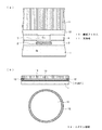
先ず、図1(a)に示すようにおよそ600μmの膜厚のシリコンウエハ(以下、Si基板)1上に酸化膜が形成され、当該酸化膜上に金属(例えば、Al)パッド2が形成され、当該Alパッド2を被覆するようにプラズマCVD法によるSiO2膜またはPSG膜から成る所定膜厚の酸化膜3を形成する。尚、特に平坦性を必要とする場合には酸化膜を例えばCMP研磨等しても良い。そして、不図示のフォトレジスト膜をマスクにAlパッド2上の酸化膜3をエッチングして当該Alパッド2の一部(表面部)を露出させる。尚、本実施形態では、前記酸化膜3の膜厚は、全体でおよそ5μm程度としている。
【0015】
次に、図1(b)に示すように前記Alパッド2及び酸化膜3上にポリイミド膜を形成し、当該ポリイミド膜を不図示のフォトレジスト膜をマスクにエッチングして前記Alパッド2上に開口部を有するポリイミド膜4を形成する。そして、前記開口部内にニッケル(Ni)5、金(Au)6を形成した後に、その上に銅(Cu)メッキしてCu7を埋め込む。また、当該Cu7上に当該Cu7の腐食防止用としてAuをメッキ形成しても良い。尚、本実施形態では、前記開口部内に埋設された導電部材(Ni,Au,Cu,Au)の膜厚は、全体でおよそ25μm程度としている。
【0016】
ここで、本プロセスが、CCDイメージセンサに採用される場合には、前記ポリイミド膜4は透明性のポリイミド膜または透明ガラスエポキシ樹脂等をスクリーン印刷法を用いて形成する必要がある。
【0017】
更に言えば、本プロセスを3次元プロセスに用いないCSPプロセスに適用するものである場合には、開口部を形成する必要はなく、ポリイミド膜4の全面塗布で構わない。
【0018】
また、図8(a)に示すように前記Alパッド2上を含む酸化膜3上にTiW21(もしくはTiW上にCuを形成しても良い。)を形成し、所定パターンと成るようにパターニングする。そして、ポリイミド膜4Aを介してCu7A(Au)を形成する、いわゆる再配線構造を採用しても良い。
【0019】
続いて、図2(a)に示すように前記Cu7(Au)上を含むポリイミド膜4上に絶縁フィルム10を貼り、当該フィルム10を介して支持板11と前記Si基板1側を貼り合わせる。
【0020】
ここで、前記支持板11は、後述するSi基板1のBG(バックグラインド)時に、Si基板1の割れ等を防止するための支持体で、例えばSi基板や酸化膜(ガラス基板)やセラミック等を利用している。尚、本実施形態では、支持体として必要な膜厚として、およそ400μm程度としている。
【0021】
また、前記フィルム10は、後述するSi基板1と支持板11との分離工程における作業性向上を図る目的で、アセトンに溶ける有機膜を採用している。尚、本実施形態では、フィルム10の膜厚をおよそ400μm程度としている。
【0022】
更に、当該フィルム10の外周部には、図2(b)に示すようにエポキシ樹脂12を充填することで、当該フィルム10を密封し、固めている。これにより、各種作業中における有機溶媒等の薬液の侵入を防止している。
【0023】
尚、Si基板1のBG工程におけるバックグラインド膜厚が少ない場合には、支持板11を貼り付ける工程は省略できる。
【0024】
次に、図3(a)に示すようにSi基板1側をBG処理して、当該Si基板1の膜厚をおよそ10〜100μm程度まで薄膜化できる。このとき、前記支持板11が、BG工程時にSi基板1を支持する。そして、BG処理したSi基板1の裏面側におよそ0.01μm程度の酸化膜13を形成する。尚、前記酸化膜13の代わりにシリコン窒化膜やポリイミドから成る有機系絶縁物を形成しても良い。更に言えば、前記BG工程において、Cu上の平坦性に左右されないため、そのままバックグラインド可能であり、作業性が良い。
【0025】
更に、図3(b)に示すように不図示のフォトレジスト膜をマスクに前記酸化膜13及びSi基板1をエッチングして開口部14を形成する。続いて、図4(a)に示すように前記開口部14から露出した酸化膜3をエッチングして、前記Alパッド2を露出させる。そして、開口部14a内の前記Alパッド2上を含む酸化膜13上を被覆するようにCVD法による酸化膜を形成し、当該酸化膜を異方性エッチングして開口部14aの側壁部に酸化膜を残膜させてサイドウォールスペーサ膜15を形成する。尚、酸化膜のCVD成膜処理温度は、200℃程度の低温度が良い。また、シリコン窒化膜を用いてサイドウォールスペーサ膜15を形成しても良い。
【0026】
次に、図4(b)に示すように前記開口部14a内にサイドウォールスペーサ膜15を介して窒化チタン(TiN)または窒化タンタル(TaN)等のバリア膜16をスパッタ形成し、当該バリア膜16を介して前記開口部14a内にCu17を埋設する。尚、本工程では、先ずバリア膜16上にCuシード、Cuメッキ処理を施し、当該Cuをアニール処理する。そして、当該Cuを開口部14a内に埋設させている。ここで、平坦性を特に必要とする場合は、当該CuをCMP研磨する。
【0027】
更に、図5(a)に示すように前記Cu17上に、当該Cu17が埋設された開口部14aの開口サイズよりも幾分広い開口を有するソルダーマスク18を形成し、当該マスク18を介して当該開口上に半田ペーストをスクリーン印刷し、当該半田ペーストをリフロー処理することで、Cu17上に半田ボール19を形成する。尚、本実施形態では、ソルダーマスク18として、200℃でイミド化可能なリカコートから成るポリイミド膜を用いている。
【0028】
尚、図8(b)に示すように前記Cu17上を含む酸化膜13上にAl膜31及びNi膜(Au膜)32を形成し、所定パターンと成るようにパターニングする。そして、ソルダーマスク18Aを介して半田ボール19Aを形成する構造を採用しても良い。
【0029】
続いて、図5(b)に示すように前記Si基板1側を前記フィルム10に到達する位置までダイシングする。
【0030】
そして、不図示のアセトン溶液槽内に当該Si基板1を浸すことで、図6(b)に示すように前記ダイシングライン(D)からアセトンが侵入し、前記フィルム10を溶解する。従って、前記Si基板1(各チップ)と支持板11とが自動的に分離され、図6(a)に示すような単体のCSPチップ20が完成する。
【0031】
このように本実施形態では、アセトンに溶解する有機系のフィルム10を用いてSi基板1と支持板11とを貼り合わせているため、ダイシング後に、Si基板1をアセトンに浸すだけで両者を簡単に分離することができ、作業性が良い。
【0032】
また、前記フィルム10の代わりに粘着力の弱いフィルムを用いて、ダイシング後に、物理的にチップを剥がすものであっても良い。更に言えば、支持板11として透明ガラスを用いる場合には、有機系フィルム10としてUVテープを貼り、ダイシング後にUV照射をし、チップを剥がせば良い。
【0033】
加えて、ダイシングした後に、例えばウエハの裏面からホットプレートで熱を加えて、ウエハと支持基板11で挟まれた有機膜(フィルム10)を溶かして軟化させることで両者を剥がすものであっても良い。このとき、フィルム10がアセトンに溶ける有機膜であるときは、200℃程度の加熱で、ポリイミド膜を利用した場合では400℃程度の加熱で当該フィルム10は溶ける。
【0034】
Si基板1と支持板11とを剥がす別形態としては、ダイシング前に、エッジのエポキシ樹脂を、ウエハを縦にして回転させ、外周だけ酸などの薬品に浸して剥がす方法もある。又、刃物をウエハとチップの間のエッジのエポキシ樹脂に入れて切り離す方法もある。そして、両方法の後、BGテープを貼ってダイシングする。
【0035】
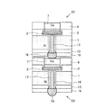
そして、図7に示すように前記単体のCSPチップ20をCu7(Au)と半田ボール19とを金属密着でCSPチップ20同士を密着(積層)させることで、3次元実装が(何層でも)可能となり、チップサイズの同じもの(メモリ等)であれば大容量化が図れる。
【0036】
【発明の効果】
本発明では、従来の3次元実装技術のように表面からSi貫通等の加工を行い、銅(Cu)のビアホールを形成するため、表面側にCMP(Chemical Mechanical Polishing)処理を必要としない。また、Cuビア形成後に当該Cuビアとパッドとを繋ぐための再配線が不要であるため、製造工数が増大することがない。
【0037】
更に言えば、Cu上の平坦性に左右されないため、そのままバックグラインド可能である。
【0038】
また、支持板11とSi基板1とは、貼り合わせた後にBG(バックグラインド)及びその後の処理をしているため、チップの膜厚は必要に応じて薄くできる。
【図面の簡単な説明】
【図1】本発明の一実施形態の半導体装置の製造方法を示す断面図である。
【図2】本発明の一実施形態の半導体装置の製造方法を示す断面図である。
【図3】本発明の一実施形態の半導体装置の製造方法を示す断面図である。
【図4】本発明の一実施形態の半導体装置の製造方法を示す断面図である。
【図5】本発明の一実施形態の半導体装置の製造方法を示す断面図である。
【図6】本発明の一実施形態の半導体装置の製造方法を示す断面図である。
【図7】本発明の一実施形態の半導体装置の製造方法を示す断面図である。
【図8】本発明の他の実施形態の半導体装置の製造方法を示す断面図である。[0001]
BACKGROUND OF THE INVENTION
The present invention relates to a method for manufacturing a semiconductor device, and more particularly to a method for manufacturing a BGA (Ball Grid Array) type semiconductor device having ball-shaped conductive terminals.
[0002]
[Prior art]
Conventionally, there is a BGA type semiconductor device as a kind of surface mount type semiconductor device. In this method, a plurality of ball-shaped conductive terminals made of a metal member such as solder are arranged in a grid pattern on one main surface of a package substrate, and bonded to a semiconductor chip mounted on the other main surface of the substrate for packaging. Is. And when incorporating in an electronic device, each conductive terminal is heat-welded to the wiring pattern on a printed circuit board, and a semiconductor chip and the external circuit mounted on a printed circuit board are electrically connected.
[0003]
Such a BGA type semiconductor device has a larger number of connection terminals than other surface mount type semiconductor devices such as SOP (Small Outline Package) and QFP (Quad Flat Package) having lead pins protruding from the side surface of the semiconductor device. It can be installed , and it is known that downsizing is advantageous.
[0004]
In recent years, this BGA type semiconductor device has been incorporated into the field of CCD image sensors, and is used as an image sensor chip for a digital camera mounted on a mobile phone that is strongly demanded for miniaturization.
[0005]
Further, three-dimensional mounting technology using wafer level CSP (Chip Size Package) and silicon (Si) penetration technology has been attracting attention. In these techniques, a method of stacking chips after stacking layers and then penetrating Si, or passing Si wafers through Si from the surface and then stacking them has been studied.
[0006]
[Problems to be solved by the invention]
However, the conventional three-dimensional mounting technology performs processing such as Si penetration from the surface to form a copper (Cu) via hole, so that CMP (Chemical Mechanical Polishing) processing is necessary on the surface side, or Cu via formation Since rewiring for connecting the Cu via and the pad later is necessary, the number of manufacturing steps increases.
[0007]
[Means for Solving the Problems]
Accordingly, in view of the above-described problem, a method for manufacturing a semiconductor device according to the present invention provides a semiconductor wafer having a metal pad formed on the surface side, and the semiconductor wafer is formed on the surface side of the semiconductor wafer on which the metal pad is formed. Bonding a support that supports the substrate through a film made of an organic film that dissolves in the solution, forming an opening that penetrates from the back surface of the semiconductor wafer to which the support is bonded to the metal pad, and the opening Forming a metal layer in the opening, forming a metal layer in the opening, dicing from the back surface of the semiconductor wafer to which the support is bonded to the film, the semiconductor wafer and the support And a step of separating the body.
[0008]
Further, the wafer and the step of bonding via a support film for supporting the wafer, across the film having a smaller outer diameter than the outer diameter of the support and the wafer and the support and the wafer In this state, only the peripheral end portion is bonded using an epoxy resin.
[0010]
Further, the film is a film having adhesiveness.
[0012]
The step of forming an electrode on the metal layer includes a step of forming a metal wiring on the metal layer and forming an electrode on the metal wiring.
[0013]
DETAILED DESCRIPTION OF THE INVENTION
Hereinafter, an embodiment according to a method of manufacturing a semiconductor device of the present invention will be described with reference to the drawings.
[0014]
First, as shown in FIG. 1A, an oxide film is formed on a silicon wafer (hereinafter referred to as Si substrate) 1 having a thickness of about 600 μm, and a metal (for example, Al)
[0015]
Next, as shown in FIG. 1B, a polyimide film is formed on the
[0016]
Here, when this process is employed in a CCD image sensor, the
[0017]
Furthermore, if the present process is applied to a CSP process that is not used in a three-dimensional process, it is not necessary to form an opening, and the entire surface of the
[0018]
Further, as shown in FIG. 8A, TiW21 (or Cu may be formed on TiW) is formed on the
[0019]
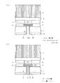
Subsequently, as shown in FIG. 2A, an
[0020]
Here, the
[0021]
The
[0022]
Furthermore, the
[0023]
If the back grind film thickness in the BG process of the
[0024]
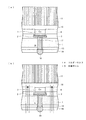
Next, as shown in FIG. 3A, the
[0025]
Further, as shown in FIG. 3B, the
[0026]
Next, as shown in FIG. 4B, a
[0027]
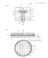
Further, as shown in FIG. 5A, a
[0028]
As shown in FIG. 8B, an
[0029]
Subsequently, as shown in FIG. 5B, the
[0030]
Then, by immersing the
[0031]
As described above, in the present embodiment, since the
[0032]
Further, instead of the
[0033]
In addition, after dicing, for example, heat is applied from the back surface of the wafer with a hot plate, and the organic film (film 10) sandwiched between the wafer and the
[0034]
As another form of peeling the
[0035]
Then, as shown in FIG. 7, the
[0036]
【The invention's effect】
In the present invention, processing such as Si penetration is performed from the surface as in the conventional three-dimensional mounting technique, and a copper (Cu) via hole is formed, so that CMP (Chemical Mechanical Polishing) processing is not required on the surface side. In addition, since the rewiring for connecting the Cu via and the pad is not required after the Cu via is formed, the number of manufacturing steps does not increase.
[0037]
Furthermore, since it does not depend on the flatness on Cu, it can be back ground as it is.
[0038]
Further, the
[Brief description of the drawings]
FIG. 1 is a cross-sectional view showing a method for manufacturing a semiconductor device according to an embodiment of the present invention.
FIG. 2 is a cross-sectional view showing a method for manufacturing a semiconductor device according to an embodiment of the present invention.
FIG. 3 is a cross-sectional view showing a method for manufacturing a semiconductor device according to an embodiment of the present invention.
FIG. 4 is a cross-sectional view showing a method for manufacturing a semiconductor device according to an embodiment of the present invention.
FIG. 5 is a cross-sectional view showing a method for manufacturing a semiconductor device according to an embodiment of the present invention.
FIG. 6 is a cross-sectional view showing a method for manufacturing a semiconductor device according to an embodiment of the present invention.
FIG. 7 is a cross-sectional view showing a method for manufacturing a semiconductor device of one embodiment of the present invention.
FIG. 8 is a cross-sectional view showing a method for manufacturing a semiconductor device according to another embodiment of the present invention.
Claims (9)
前記半導体ウエハの前記金属パッドが形成された表面側に対して、当該半導体ウエハを支持する支持体を溶液に溶ける有機膜から成るフィルムを介して貼り合わせる工程と、
前記支持体が貼り合わされた前記半導体ウエハの裏面から前記金属パッドまで貫通する開口を形成する工程と、
前記開口の側壁部に絶縁膜を形成した後に、当該開口内に金属層を形成する工程と、
前記支持体が貼り合わされた前記半導体ウエハの裏面から前記フィルムまでダイシングする工程と、
前記半導体ウエハと前記支持体とを分離する工程とを有することを特徴とする半導体装置の製造方法。Prepare a semiconductor wafer with metal pads on the surface side,
Bonding the support for supporting the semiconductor wafer to the surface side of the semiconductor wafer on which the metal pads are formed via a film made of an organic film that dissolves in a solution ;
Forming an opening penetrating from the back surface of the semiconductor wafer to which the support is bonded to the metal pad;
Forming an insulating film on the side wall of the opening and then forming a metal layer in the opening;
Dicing from the back surface of the semiconductor wafer to which the support is bonded to the film;
A method for manufacturing a semiconductor device, comprising the step of separating the semiconductor wafer and the support.
Priority Applications (1)
| Application Number | Priority Date | Filing Date | Title |
|---|---|---|---|
| JP2002111571A JP4212293B2 (en) | 2002-04-15 | 2002-04-15 | Manufacturing method of semiconductor device |
Applications Claiming Priority (1)
| Application Number | Priority Date | Filing Date | Title |
|---|---|---|---|
| JP2002111571A JP4212293B2 (en) | 2002-04-15 | 2002-04-15 | Manufacturing method of semiconductor device |
Related Child Applications (2)
| Application Number | Title | Priority Date | Filing Date |
|---|---|---|---|
| JP2006088904A Division JP4425235B2 (en) | 2006-03-28 | 2006-03-28 | Semiconductor device and manufacturing method thereof |
| JP2006292233A Division JP4443549B2 (en) | 2006-10-27 | 2006-10-27 | Manufacturing method of semiconductor device |
Publications (3)
| Publication Number | Publication Date |
|---|---|
| JP2003309221A JP2003309221A (en) | 2003-10-31 |
| JP2003309221A5 JP2003309221A5 (en) | 2005-09-22 |
| JP4212293B2 true JP4212293B2 (en) | 2009-01-21 |
Family
ID=29394327
Family Applications (1)
| Application Number | Title | Priority Date | Filing Date |
|---|---|---|---|
| JP2002111571A Expired - Fee Related JP4212293B2 (en) | 2002-04-15 | 2002-04-15 | Manufacturing method of semiconductor device |
Country Status (1)
| Country | Link |
|---|---|
| JP (1) | JP4212293B2 (en) |
Families Citing this family (41)
| Publication number | Priority date | Publication date | Assignee | Title |
|---|---|---|---|---|
| JP4340517B2 (en) | 2003-10-30 | 2009-10-07 | Okiセミコンダクタ株式会社 | Semiconductor device and manufacturing method thereof |
| TWI249767B (en) * | 2004-02-17 | 2006-02-21 | Sanyo Electric Co | Method for making a semiconductor device |
| JP2005235860A (en) * | 2004-02-17 | 2005-09-02 | Sanyo Electric Co Ltd | Semiconductor device and manufacturing method thereof |
| JP4850392B2 (en) | 2004-02-17 | 2012-01-11 | 三洋電機株式会社 | Manufacturing method of semiconductor device |
| CN101373747B (en) * | 2004-03-16 | 2011-06-29 | 株式会社藤仓 | Device with through-hole interconnection and method for manufacturing the same |
| JP2005303258A (en) * | 2004-03-16 | 2005-10-27 | Fujikura Ltd | Device and method for manufacturing the same |
| JP2005277173A (en) * | 2004-03-25 | 2005-10-06 | Sanyo Electric Co Ltd | Semiconductor device, and its manufacturing method |
| JP4544902B2 (en) * | 2004-04-26 | 2010-09-15 | 三洋電機株式会社 | Semiconductor device and manufacturing method thereof |
| JP4746847B2 (en) * | 2004-04-27 | 2011-08-10 | 三洋電機株式会社 | Manufacturing method of semiconductor device |
| TWI272683B (en) | 2004-05-24 | 2007-02-01 | Sanyo Electric Co | Semiconductor device and manufacturing method thereof |
| JP4518995B2 (en) * | 2004-05-24 | 2010-08-04 | 三洋電機株式会社 | Semiconductor device and manufacturing method thereof |
| JP4376715B2 (en) | 2004-07-16 | 2009-12-02 | 三洋電機株式会社 | Manufacturing method of semiconductor device |
| JP4373866B2 (en) | 2004-07-16 | 2009-11-25 | 三洋電機株式会社 | Manufacturing method of semiconductor device |
| JP4524156B2 (en) * | 2004-08-30 | 2010-08-11 | 新光電気工業株式会社 | Semiconductor device and manufacturing method thereof |
| JP4139803B2 (en) | 2004-09-28 | 2008-08-27 | シャープ株式会社 | Manufacturing method of semiconductor device |
| JP4966487B2 (en) | 2004-09-29 | 2012-07-04 | オンセミコンダクター・トレーディング・リミテッド | Semiconductor device and manufacturing method thereof |
| TWI267183B (en) | 2004-09-29 | 2006-11-21 | Sanyo Electric Co | Semiconductor device and manufacturing method of the same |
| JP4936695B2 (en) * | 2004-09-29 | 2012-05-23 | オンセミコンダクター・トレーディング・リミテッド | Semiconductor device and manufacturing method thereof |
| JP4246132B2 (en) | 2004-10-04 | 2009-04-02 | シャープ株式会社 | Semiconductor device and manufacturing method thereof |
| JP4845368B2 (en) * | 2004-10-28 | 2011-12-28 | オンセミコンダクター・トレーディング・リミテッド | Semiconductor device and manufacturing method thereof |
| TWI303864B (en) | 2004-10-26 | 2008-12-01 | Sanyo Electric Co | Semiconductor device and method for making the same |
| JP5036127B2 (en) * | 2004-10-26 | 2012-09-26 | オンセミコンダクター・トレーディング・リミテッド | Manufacturing method of semiconductor device |
| JP4443379B2 (en) | 2004-10-26 | 2010-03-31 | 三洋電機株式会社 | Manufacturing method of semiconductor device |
| JP4873517B2 (en) * | 2004-10-28 | 2012-02-08 | オンセミコンダクター・トレーディング・リミテッド | Semiconductor device and manufacturing method thereof |
| JP4783906B2 (en) | 2004-11-30 | 2011-09-28 | 国立大学法人九州工業大学 | Packaged stacked semiconductor device and manufacturing method thereof |
| US7485967B2 (en) | 2005-03-10 | 2009-02-03 | Sanyo Electric Co., Ltd. | Semiconductor device with via hole for electric connection |
| JP2007036060A (en) * | 2005-07-28 | 2007-02-08 | Sanyo Electric Co Ltd | Semiconductor device and manufacturing method thereof |
| JP4745007B2 (en) * | 2005-09-29 | 2011-08-10 | 三洋電機株式会社 | Semiconductor device and manufacturing method thereof |
| JP2007180395A (en) * | 2005-12-28 | 2007-07-12 | Sanyo Electric Co Ltd | Manufacturing method of semiconductor device |
| JP4619308B2 (en) * | 2006-03-07 | 2011-01-26 | 三洋電機株式会社 | Semiconductor device manufacturing method and supporting tape |
| JP5242063B2 (en) * | 2006-03-22 | 2013-07-24 | 株式会社フジクラ | Wiring board manufacturing method |
| JP2007305960A (en) * | 2006-04-14 | 2007-11-22 | Sharp Corp | Semiconductor device and manufacturing method |
| JP2008041987A (en) * | 2006-08-08 | 2008-02-21 | Tokyo Ohka Kogyo Co Ltd | Method and equipment for peeling support plate and wafer |
| JP2009272490A (en) * | 2008-05-08 | 2009-11-19 | Oki Semiconductor Co Ltd | Semiconductor device and method of manufacturing semiconductor device |
| US9245765B2 (en) | 2009-10-16 | 2016-01-26 | Empire Technology Development Llc | Apparatus and method of applying a film to a semiconductor wafer and method of processing a semiconductor wafer |
| JP5258735B2 (en) * | 2009-11-13 | 2013-08-07 | セミコンダクター・コンポーネンツ・インダストリーズ・リミテッド・ライアビリティ・カンパニー | Semiconductor device |
| JP5412316B2 (en) | 2010-02-23 | 2014-02-12 | パナソニック株式会社 | Semiconductor device, stacked semiconductor device, and manufacturing method of semiconductor device |
| JP2010251791A (en) * | 2010-06-24 | 2010-11-04 | Sanyo Electric Co Ltd | Semiconductor device and method of manufacturing the same |
| JP5870493B2 (en) * | 2011-02-24 | 2016-03-01 | セイコーエプソン株式会社 | Semiconductor devices, sensors and electronic devices |
| JP2015115446A (en) | 2013-12-11 | 2015-06-22 | 株式会社東芝 | Semiconductor device manufacturing method |
| JP2019145737A (en) | 2018-02-23 | 2019-08-29 | ソニーセミコンダクタソリューションズ株式会社 | Semiconductor device and manufacturing method of semiconductor device |
-
2002
- 2002-04-15 JP JP2002111571A patent/JP4212293B2/en not_active Expired - Fee Related
Also Published As
| Publication number | Publication date |
|---|---|
| JP2003309221A (en) | 2003-10-31 |
Similar Documents
| Publication | Publication Date | Title |
|---|---|---|
| JP4212293B2 (en) | Manufacturing method of semiconductor device | |
| KR100552356B1 (en) | Method of manufacturing semiconductor device | |
| US7399683B2 (en) | Manufacturing method of semiconductor device | |
| TWI622144B (en) | Fingerprint sensor device and method | |
| CN107026092B (en) | Method of manufacturing fingerprint scanner and semiconductor device | |
| KR100938970B1 (en) | Semiconductor device and manufacturing method thereof | |
| KR100671921B1 (en) | Semiconductor device and manufacturing method thereof | |
| US8922013B2 (en) | Through via package | |
| JP4544876B2 (en) | Manufacturing method of semiconductor device | |
| KR101157726B1 (en) | Ultra-thin stacked chips packaging | |
| US20050167812A1 (en) | Semiconductor device, three-dimensional semiconductor device, and method of manufacturing semiconductor device | |
| JP4522574B2 (en) | Method for manufacturing semiconductor device | |
| JP2004055628A (en) | Semiconductor device of wafer level and its manufacturing method | |
| JP2005072554A (en) | Semiconductor device and its manufacturing method | |
| US6989291B2 (en) | Method for manufacturing circuit devices | |
| JP3459234B2 (en) | Semiconductor device and manufacturing method thereof | |
| JP2009033153A (en) | Interconnecting structure for semiconductor device package and method of the same | |
| JP4425235B2 (en) | Semiconductor device and manufacturing method thereof | |
| JP4215571B2 (en) | Manufacturing method of semiconductor device | |
| JP4334397B2 (en) | Semiconductor device and manufacturing method thereof | |
| JP4638614B2 (en) | Method for manufacturing semiconductor device | |
| JP4443549B2 (en) | Manufacturing method of semiconductor device | |
| JP4286264B2 (en) | Semiconductor device and manufacturing method thereof | |
| JP2004153260A (en) | Semiconductor device and method of manufacturing same | |
| JP4371719B2 (en) | Semiconductor device and manufacturing method thereof |
Legal Events
| Date | Code | Title | Description |
|---|---|---|---|
| A521 | Request for written amendment filed |
Free format text: JAPANESE INTERMEDIATE CODE: A523 Effective date: 20050415 |
|
| A621 | Written request for application examination |
Free format text: JAPANESE INTERMEDIATE CODE: A621 Effective date: 20050415 |
|
| A977 | Report on retrieval |
Free format text: JAPANESE INTERMEDIATE CODE: A971007 Effective date: 20050801 |
|
| A131 | Notification of reasons for refusal |
Free format text: JAPANESE INTERMEDIATE CODE: A131 Effective date: 20060905 |
|
| A521 | Request for written amendment filed |
Free format text: JAPANESE INTERMEDIATE CODE: A523 Effective date: 20061026 |
|
| A521 | Request for written amendment filed |
Free format text: JAPANESE INTERMEDIATE CODE: A523 Effective date: 20061122 |
|
| A131 | Notification of reasons for refusal |
Free format text: JAPANESE INTERMEDIATE CODE: A131 Effective date: 20070906 |
|
| A521 | Request for written amendment filed |
Free format text: JAPANESE INTERMEDIATE CODE: A523 Effective date: 20071031 |
|
| TRDD | Decision of grant or rejection written | ||
| A01 | Written decision to grant a patent or to grant a registration (utility model) |
Free format text: JAPANESE INTERMEDIATE CODE: A01 Effective date: 20081002 |
|
| A01 | Written decision to grant a patent or to grant a registration (utility model) |
Free format text: JAPANESE INTERMEDIATE CODE: A01 |
|
| A61 | First payment of annual fees (during grant procedure) |
Free format text: JAPANESE INTERMEDIATE CODE: A61 Effective date: 20081028 |
|
| FPAY | Renewal fee payment (event date is renewal date of database) |
Free format text: PAYMENT UNTIL: 20111107 Year of fee payment: 3 |
|
| R151 | Written notification of patent or utility model registration |
Ref document number: 4212293 Country of ref document: JP Free format text: JAPANESE INTERMEDIATE CODE: R151 |
|
| FPAY | Renewal fee payment (event date is renewal date of database) |
Free format text: PAYMENT UNTIL: 20111107 Year of fee payment: 3 |
|
| A521 | Request for written amendment filed |
Free format text: JAPANESE INTERMEDIATE CODE: A523 Effective date: 20061026 |
|
| FPAY | Renewal fee payment (event date is renewal date of database) |
Free format text: PAYMENT UNTIL: 20121107 Year of fee payment: 4 |
|
| R250 | Receipt of annual fees |
Free format text: JAPANESE INTERMEDIATE CODE: R250 |
|
| FPAY | Renewal fee payment (event date is renewal date of database) |
Free format text: PAYMENT UNTIL: 20121107 Year of fee payment: 4 |
|
| FPAY | Renewal fee payment (event date is renewal date of database) |
Free format text: PAYMENT UNTIL: 20131107 Year of fee payment: 5 |
|
| R250 | Receipt of annual fees |
Free format text: JAPANESE INTERMEDIATE CODE: R250 |
|
| R250 | Receipt of annual fees |
Free format text: JAPANESE INTERMEDIATE CODE: R250 |
|
| R250 | Receipt of annual fees |
Free format text: JAPANESE INTERMEDIATE CODE: R250 |
|
| R250 | Receipt of annual fees |
Free format text: JAPANESE INTERMEDIATE CODE: R250 |
|
| R250 | Receipt of annual fees |
Free format text: JAPANESE INTERMEDIATE CODE: R250 |
|
| R250 | Receipt of annual fees |
Free format text: JAPANESE INTERMEDIATE CODE: R250 |
|
| R250 | Receipt of annual fees |
Free format text: JAPANESE INTERMEDIATE CODE: R250 |
|
| R250 | Receipt of annual fees |
Free format text: JAPANESE INTERMEDIATE CODE: R250 |
|
| R250 | Receipt of annual fees |
Free format text: JAPANESE INTERMEDIATE CODE: R250 |
|
| LAPS | Cancellation because of no payment of annual fees |