JP4167010B2 - Display substrate processing equipment - Google Patents
Display substrate processing equipment Download PDFInfo
- Publication number
- JP4167010B2 JP4167010B2 JP2002177523A JP2002177523A JP4167010B2 JP 4167010 B2 JP4167010 B2 JP 4167010B2 JP 2002177523 A JP2002177523 A JP 2002177523A JP 2002177523 A JP2002177523 A JP 2002177523A JP 4167010 B2 JP4167010 B2 JP 4167010B2
- Authority
- JP
- Japan
- Prior art keywords
- display substrate
- receiving
- support
- base
- disposed
- Prior art date
- Legal status (The legal status is an assumption and is not a legal conclusion. Google has not performed a legal analysis and makes no representation as to the accuracy of the status listed.)
- Expired - Lifetime
Links
Images


Description
【0001】
【発明の属する技術分野】
本発明は、薄膜トランジスタを形成したガラス基板や表示パネルのような表示用基板を処理する装置に関する。
【0002】
【従来の技術】
液晶表示パネルのように高密度に配置された多数の画素を有する表示用パネルにおいては、欠陥画素に修正加工を行って、その表示用パネルを不良品とすることなく、良品として用いることが行われている。
【0003】
そのような修正加工技術は、一般に、欠陥画素を有する表示用パネルを二次元的に移動させるXYステージに載置し、その表示用パネルに照明用光を下方から照射しつつ、欠陥画素のような欠陥箇所に加工用レーザ光線を上方から照射することにより、行われている(例えば、特開平9−90304号、特開2001−91919号、特開2002−40674号)。
【0004】
この種の修正加工を行う処理装置においては、加工用レーザ光線及び照明用光をそれぞれ表示用パネルに上方及び下方から照射しなければならないことから、修正加工を行うべき表示用パネルの寸法に応じた大きさの開口をXYステージに形成している。このため、従来の処理装置では、寸法が異なる表示用パネルに変更されるたびに、XYステージを交換しなければならない。
【0005】
上記の課題を解決するために、液晶表示パネルのように矩形の表示用基板の辺を受けるように配置された長方形の4つの枠材を受け材として用い、1つの枠材を固定受け材とし、この固定受け材と対向する他の1つの枠材を固定枠材に対しX及びY方向に二次元的に移動させる第1の可動枠材とし、残りの2つの枠材を固定受けに対しX方向又はY方向に移動させる第2及び第3の可動受け材とした処理装置が提案されている(特開2002−91336号)。
【0006】
この処理装置においては、大きさが異なる表示用基板に変更されても、その表示用基板の各辺を受け材に受けることができるように、各受け材を長方形の板の形に形成しており、また各可動受け材を固定受け材に対して移動させることにより、4つの受け材で形成される開口の大きさを処理すべき表示用基板の大きさに適合させている。
【0007】
【解決しようとする課題】
しかし、上記の処置装置では、処理可能の最大寸法の表示用基板を受けることができる長さ寸法を有する受け材を用いなければならないし、受け材の移動方向が受け材毎に異なるから、受け材の支持機構が大型であると共に、複雑である。
【0008】
本発明の目的は、大きさの異なる表示用基板を受けることができるにもかかわらず、小型で簡単な構造の受け材支持機構とすることにある。
【0009】
【解決手段、作用、効果】
本発明に係る処理装置は、処理すべき表示用基板の隅角部を個々に受ける4つの受けベースと、隣り合う受けベースを前記表示用基板と平行の面内で相寄り相離れる方向に移動可能に支持する支持機構とを含む。
【0010】
表示用基板は、その隅角部を受けベースに受けられる。大きさが異なる表示用基板に変更されると、隣り合う受けベースが表示用基板の大きさに応じて表示用基板と平行の面内で相寄り相離れる方向に移動される。
【0011】
本発明によれば、表示用基板の隅角部を受けベースに受けると共に、隣り合う受けベースを相寄り相離れる方向に移動させるから、受けベースの移動方向が同じになり、したがって受けベースの支持機構が小型化すると共に、簡単な構造になる。
【0012】
本発明に係る処理装置は、さらに、前記表示用基板の隣り合う一対の第1及び第2の辺の一端部が当接可能に1つの前記受けベースに配置された第1のストッパと、前記第1の辺の他端部が当接可能に前記1つの受けベースの隣の受けベースに配置された第2のストッパとを含むことができる。そのようにすれば、表示用基板の隣り合う2つの辺をストッパに当接させることにより、装置に対する表示用基板に位置決めをすることができる。
【0013】
本発明に係る処理装置は、さらに、前記表示用基板を前記第1のストッパに向けて押圧すべく前記隣の受けベースに配置された第1のプッシャと、前記表示用基板を前記第1及び第2のストッパに向けて押圧すべく残りの前記受けベースに配置された第2のプッシャとを含むことができる。そのようにすれば、装置に対する表示用基板に位置決めがストッパとプッシャとにより行われる。
【0014】
本発明に係る処理装置において、前記支持機構は、第1の方向に隣り合う受けベースを前記第1の方向へ移動可能に前記隣り合う受けベースの対毎に受ける一対の第1の支持手段と、前記第1の支持手段を前記第1の方向と交差する第2の方向へ移動可能に受ける第2の支持手段とを含む。これにより、第1及び第2の方向への各受けベースの移動が円滑及び正確になり、また支持機構がより小型化すると共に、より簡単な構造になる。
【0015】
本発明に係る処理装置は、さらに、前記第2の方向に隣り合う受けベースを前記第2の方向へ移動可能に連結する一対の連結手段を含むことができる。そのようにすれば、第2の方向への受けベースの移動がより円滑及び正確になる。
【0016】
本発明に係る処理装置は、さらに、前記第2の支持手段を前記表示用基板と平行の面内で二次元的に移動させるべく前記第2の支持手段を支持する支持台と、照明光を前記表示用基板に下方側から照射すべく前記表示用基板と前記支持台との間に配置された照明手段と、加工用光線を前記表示用基板に上方から照射する光線照射手段とを含む。これにより、処理装置を、表示用基板に修正加工を行う修正装置として用いることができる。また、修正すべき箇所を明示することができるし、照明手段のための大きな配置空間を必要としない。
【0017】
本発明に係る処理装置において、前記照明手段は、前記支持台が配置された基台に少なくとも前記支持台を跨ぐ状態に配置されたアームと、該アームに配置されて前記照明光を前記表示用基板に照射する光ファイバ又は光源とを含む。これにより、照明手段のための配置空間をより小さくすることができる。
【0018】
本発明に係る処理装置は、さらに、前記第2の支持手段を前記表示用基板と平行の面内で二次元的に移動させると共に前記表示用基板に垂直の軸線方向へ移動させるべく前記第2の支持手段を受けるステージと、前記受けベースから上方に間隔をおいて配置された1以上のプローブユニットとを含み、前記プローブユニットは前記表示用基板に押圧される複数の接触子を備えていてもよい。そのようにすれば、処理装置を、表示用パネルやガラス基板のような表示用基板の検査装置、特に点灯検査装置として用いることができる。
【0019】
【発明の実施の形態】
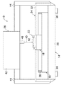
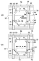
図1〜図3を参照するに、処理装置10は、液晶表示パネルのような表示用基板12に修正加工のための処理を行う修正装置として用いられる。表示用基板12は、欠陥画素のような欠陥箇所を有しており、その欠陥箇所をレーザ光線のような加工用光線により修正される。
【0020】
本発明においては、図2において、左右方向をX方向といい、紙面に垂直の方向をY方向といい、上下方向を上下方向又はZ方向という。
【0021】
処理装置10は、基台14と、基台14の上に設置された第1の支持台16と、第1の支持台16の上に設置された第2の支持台18と、第1の支持台16に組み付けられたフェンス20と、処理すべき表示用基板12を受ける受けステージ22と、受けられた表示用基板12に下方から照明光を照射する照明装置24と、受けられた表示用基板12に上方から加工用の光線を照射する光線照射装置26とを含む。
【0022】
基台14は、厚い板状部材28の4つの隅部に4つの脚部材30を取り付けたテーブルの形を有しており、また処理装置10のフレーム(図示せず)に設置される。
【0023】
第1の支持台16は平面サーボモータステージとして市販されている、XY方向への二次元ステージの固定子装置であり、第2の支持台18はそのような平面サーボモータステージの可動子装置である。平面サーボモータステージは、駆動源としてリニアモータを用いており、リニアモータをサーボ制御すなわち位置制御している。
【0024】
図示の例では、第1及び第2の支持台16及び18は、両者で、受けステージ22をこれに受けられた表示用基板12と平行の面内でXY方向に二次元的に移動させるステージを構成している。
【0025】
しかし、第1及び第2の支持台16及び18は、平面サーボモータステージ以外の二次元ステージを用いてもよいし、受けステージ22を上下方向に移動させるZステージの機能を兼ね備えたXYZの三次元ステージに構成されていてもよく、さらに受けステージ22をZ軸線の周りに角度的に回転させるθステージを兼ね備えたXYZθのステージに構成されていてもよい。
【0026】
フェンス20は、矩形の枠の形を有しており、また第1の支持台16の上に取り付けられている。フェンス20はXYステージの可動子装置としての第2の支持台18が固定子装置としての第1の支持台16から落下することを防止するためのものであり、したがってフェンス20を備えていなくてもよい。
【0027】
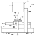
照明装置24は、門型に形成されたアーム32を備えている。アーム32は、第1の支持台16及び第2の支持台18を跨ぐ状態に基台14に取り付けられている。
【0028】
アーム32には、図4から図6に示すように、光ファイバ34が配置されている。光ファイバ34は、図示しない光源で発生された光を受け、その光をスポット状の照明光36として、アーム32の上部部材の長手方向中央部に形成された穴38から表示用基板12の下面に照射する。
【0029】
光ファイバ34を用いる代わりに、図7に示すように、スポット状の照明光36を穴38から表示用基板12の下面に照射する光源36aをアーム32に配置してもよい。
【0030】
光線照射装置26は、レーザ光線を加工用光線40として発生するレーザ装置であり、レーザ発生器及び光学系を筐体42に収容している。光線照射装置26は、加工用光線40を表示用基板12の欠陥箇所にその真上から照射するように、筐体42において複数の支持部材44により基台14に取り付けられている。加工用光線40は、レーザ鏡筒46から出力される。
【0031】
照明装置24及び光線照射装置26は、照明光36及び加工用光線40が表示用基板12のXY方向における同一箇所に照射されるように、予め設定されている。
【0032】
第1及び第2の支持台16,18は、表示用基板12を照明装置24と光線照射装置26との間に位置させて、照明光36及び加工用光線40が表示用基板12の欠陥箇所に照射されるように、表示用基板12及び受けステージ22を移動させるときに駆動される。
【0033】
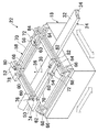
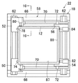
受けステージ22は、図4から図8に示すように、表示用基板12の4つの隅角部を個々に受ける4つの受けベース50,52,54,56と、隣り合う受けベース50及び52並びに54及び56を表示用基板12と平行の面内で相寄り相離れる方向(XY方向)に移動可能に支持する支持機構58とを含む。
【0034】
受けベース50,52,54,56の各々は、矩形の板部材により形成されており、また1つの隅角部がL字状に欠如された欠如部60を有しており、さらに4つの受けベース50,52,54,56により矩形をした仮想的な開口又は空間を形成するように、欠如部60を中央に向けた状態に支持機構58に取り付けられている。
【0035】
支持機構58は、Y方向に隣り合う受けベース50及び52の対並びに54及び56の対をリニアガイドレール62及び62に対毎のリニアガイド64及び64を介してY方向へ移動可能に受け、両リニアガイドレール62及び62をリニアガイドレール66及び66に複数のリニアガイド68を介してX方向へ移動可能に受けている。このため、各受けベースは、X方向及びY方向に移動可能である。
【0036】
受けステージ22は、また、X方向に隣り合う受けベース50及び54の対並びに52及び56の対をそれぞれX方向へ移動可能に対毎に連結する一対の連結棒70及び70と、連結棒70及び70がそれぞれその長手方向に移動可能に貫通する複数のボールブッシュ72及び72とを含む。
【0037】
連結棒70及び70は、それぞれ、受けベース50及び52から相手側の受けベース54及び56に向けて伸びるように、受けベース50及び52に取り付けられている。ボールブッシュ72及び72は、それぞれ、受けベース54及び56に取り付けられている。各連結棒70として、リニアシャフトを用いることができる。
【0038】
図示の例では、リニアガイドレール62,62及びリニアガイド64,64は第1の支持手段を形成しており、リニアガイドレール66,66及びリニアガイド68は第2の支持手段を形成しており、連結棒70,70及びボールブッシュ72,72は連結手段を形成している。
【0039】
図示の例では、照明装置24のアーム32は、両リニアガイド66,66の間にあって第2の支持台18と両リニアガイド62,62の間を伸びている。
【0040】
受けステージ22は、さらに、表示用基板12の隣り合う一対の第1及び第2辺(Y辺及びX辺)の一端部が個々に当接可能に1つの受けベース50に配置された一対のストッパ74,76と、第1の辺(Y辺)の他端部が当接可能に、受けベース50に対しY方向に隣り合う受けベース52に配置されたストッパ78と、表示用基板12をストッパ74に向けて押圧すべく受けベース52に配置されたプッシャ80と、表示用基板12をストッパ76,78に向けて押圧すべく受けベース54及び56にそれぞれ配置された一対のプッシャ82及び84とを含む。
【0041】
ストッパ74,76,78の各々は、ピンの形状を有しており、したがって表示用基板12を受けステージ22に対して位置決める位置決めピンとして作用するのみならず、表示用基板12を受けステージ22に設置するときに表示用基板12を案内するガイドピンとして作用する。
【0042】
プッシャ80,82,84の各々は、プッシュ片を表示用基板12の所定の辺に押すプランジャを備えており、プランジャにおいて所定の受けベースに取り付けられている。
【0043】
表示用基板12の処理に先立って、受けベース50,52,54,56が、処理すべき表示用基板12の大きさに適合する位置に移動され、その位置に止めねじのような適宜な部材により一時的に維持される。この作業は、光線照射装置16が作業の妨げにならない位置において行われる。
【0044】
次いで、処理すべき表示用基板12が、4つの隅角部を受けステージ22の受けベース50,52,54,56に受けられる状態に、受けステージ22に載せられる。
【0045】
次いで、表示用基板12が、プッシャ80,82,84により押されて、所定の辺を所定のストッパ74,76,78に当接される。これにより、受けステージ22に対する表示用基板12に位置決めが自動的に行われる。
【0046】
次いで、受けステージ22が、第1及び第2の支持台16,18により、照明装置24と光線照射装置26との間に移動されると共に、照明装置24と光線照射装置26との間でさらに移動される。これにより、表示用基板12は、照明光36及び加工用光線40が欠陥箇所86に照射されない、図8(A)に示す位置を経て、照明光36及び加工用光線40が欠陥箇所86に照射される、図8(B)に示す位置に移動される。
【0047】
欠陥箇所86のXY座標位置は、表示用基板12の良否が、点灯検査装置のような検査装置により検査されたとき、知ることができる。したがって、欠陥箇所86のXY座標位置をその表示用基板12の番号と共にメモリに予め記憶しておき、記憶しているXY座標位置を用いて、第1及び第2の支持台16及び18を制御装置により制御しつつ駆動させてもよい。この場合、照明装置24を省略してもよい。
【0048】
しかし、照明光36を表示用基板12に照射させて、その照射箇所を目視により確認しつつ、照明光36が欠陥箇所86に照射するように第1及び第2の支持台16,18により受けステージ22を移動させて、照明光36及び加工用光線40が欠陥箇所に照射する位置に表示用基板12を移動させてもよい。
【0049】
上記の代わりに、微弱な加工用光線40を表示用基板12に照射して、その照射箇所を目視により確認しつつ、微弱な加工用光線40が欠陥箇所68に照射するように第1及び第2の支持台16,18により受けステージ22を移動させて、加工用光線40が欠陥箇所68に照射する位置に表示用基板12を移動させてもよい。
【0050】
次いで、加工用光線40が欠陥箇所86に照射される。これにより、欠陥箇所86に存在する、画素要素、配線、回路素子等が破壊又は切断されて、表示用基板12が点灯されたときに欠陥箇所86が黒色表示となるように修正される。欠陥箇所68が修正されたか否かの確認は、照明光36を欠陥箇所68に下側から照射して、欠陥箇所68のパターンが切断又は破壊されたか否かを確認することにより、行うことができる。
【0051】
処理装置10によれば、以下のような種々の利点を生じる
【0052】
表示用基板12の隅角部を受けベース50,52,54,56に受けると共に、隣り合う受けベースを相寄り相離れる方向に移動させるから、受けベースの移動方向がいずれもXY方向と同じになり、したがって支持機構58が小型化すると共に、簡単な構造になる。
【0053】
支持機構58が、Y方向に隣り合う受けベース50,52の対及び54,56の対をリニアガイドレール62及び62にY方向へ移動可能に受けると共に、リニアガイドレール62,62をリニアガイド66,66にX方向へ移動可能に受けるから、XY方向への各受けベースの移動が円滑及び正確になり、また支持機構58がより小型化すると共に、より簡単な構造になる。
【0054】
X方向に隣り合う受けベース50,54及び52,56を一対の連結棒70及び一対のボールブッシュ72によりX方向へ移動可能に連結しているから、X方向への受けベースの移動がより円滑及び正確になる。
【0055】
照明装置24のアーム32が、リニアガイドレール66,66の間にあって第2の支持台18とリニアガイドレール62,62の間を通っているから、修正すべき箇所を明示することができるのみならず、照明装置24のための大きな配置空間を必要としない。
【0056】
照明装置24のアーム32が第1及び第2の支持台16及び18を跨ぐ状態に基台14に配置され、照明光36のための光ファイバ34がアーム32に配置されているから、照明装置24のための配置空間をより小さくなる。
【0057】
上記の実施例では、表示用基板12の隅角部を受けベース50,52,54,56に直接載せているが、図9に受けステージ22の平面図を示すと共に、図10に受けベース52を代表して示すように、矩形の開口87を有する枠部材88を受けベース50,52,54,56に載せ、この枠部材88に表示用基板12の隅角部を載せることにより、枠部材88を介して表示用基板12の隅角部を含む4辺部を受けベース50,52,54,56に載せてもよい。
【0058】
図9及び図10に示す実施例において、枠部材88は、受けベース50,52,54,56に取り外し可能に取り付けることができる。また、表示用基板12をプッシャ80,82,84により所定のストッパに向けて押すようにしてもよい。
【0059】
上記いずれの実施例においても、照明装置24を少なくともY方向に、好ましくはXY方向に移動させるようにしてもよい。この場合、第2の支持台18は受けステージージ22及び表示用基板12を少なくともY方向へ移動させるステージとしなくてもよい。
【0060】
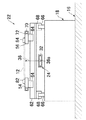
図11を参照するに、処理装置90は、表示用パネルやガラス基板のような表示用基板12の、特に点灯検査のための装置として用いられる。
【0061】
処理装置90においては、検査ステージ92を第1及び第2の支持台16及び18の代わりに備えており、バックライトユニット94を検査ステージ92に配置し、表示用基板12を受ける受けステージ22をバックライトユニット94に配置している。
【0062】
検査ステージ92は、バックライトユニット94、受けステージ22及び表示用基板12を、X,Y,Zの三方向に移動させると共に、Z軸線の周りに回転させる公知の装置であり、また処理装置90の板状の下部フレーム96に設置されている。バックライトユニット94も、表示用基板12を背面から照明する公知の装置である。
【0063】
処理装置90は、また、プローブユニット98を処理装置90の板状の上部フレーム100に、受けステージ22から上方に間隔をおいた状態に配置している。プローブユニット98は、基板102を上部フレーム100に取り付け、それぞれが表示用基板12の電極に押圧される複数の接触子104を備えた複数のプローブブロック106を基板102に取り付けている。
【0064】
基板100は、表示用基板12よりやや大きい開口108を有しており、開口108が上部フレーム100の開口110と対向するように上部フレーム100の下側に取り付けられている。プローブブロック106は、接触子104の先端が下方に突出するように基板102に取り付けられている。接触子104は、図示の例では、ニードルタイプのプローブである。
【0065】
検査時、表示用基板12は、検査ステージ92により、接触子104に対する位置合わせをされた後、上昇されて、電極を接触子104に押圧される。この状態で接触子104を介して通電される。このとき、バックライトユニット94は点灯されており、したがって表示用基板12の点灯状態は開口110及び108を介して観察される。
【0066】
処理装置90において、点灯検査の結果、その表示用基板12が欠陥箇所を有しているときは、加工用光線40を欠陥箇所に照射して、修正するようにしてもよい。
【0067】
上記実施例では、いずれも、表示用基板12を水平の状態で処理しているが、本発明は、表示用基板12を斜めの状態、上下に立てた状態等で処理する装置にも適用することができる。それゆえに、本発明でいう各方向特に上下方向は、必ずしも重力の方向と一致するとは限られず、むしろ表示用基板に垂直のいわゆるZ方向のことを意味する。
【0068】
本発明は、上記実施例に限定されず、その趣旨を逸脱しない限り、種々変更することができる。
【図面の簡単な説明】
【図1】本発明に係る処理装置の一実施例を示す斜視図である。
【図2】図1に示す処理装置の正面図である。
【図3】図1に示す処理装置の右側面図である。
【図4】図1に示す処理装置で用いる受けステージの一実施例を示す斜視図である。
【図5】図4に示す受けステージに表示用基板を載置した状態を示す斜視図である。
【図6】図4に示す受けステージの平面図である。
【図7】図4に示す受けステージの右側面図である。
【図8】図4に示す受けステージの動作を説明するための図である。
【図9】図4に示す受けステージにおいて枠部材を用いる実施例を示す平面図である。
【図10】図9における10−10線に沿って得た断面図である。
【図11】本発明に係る処理装置の他の実施例を示す縦断面図である。
【符号の説明】
10,90 処理装置
12 表示用基板
14 基台
16,18 第1及び第2の支持台
22 受けステージ
24 照明装置
26 加工用光線の照射装置
32 照明装置のアーム
34 照明光用の光ファイバ
36 照明光
36a 照明光用の光源
38 照明光用の穴
40 加工用光線
50,52,54,56 受けベース
58 支持機構
62,66 リニアガイドレール
64,68 リニアガイド
70 連結棒
72 ボールブッシュ
74,76,78 ストッパ
80,82,84 プッシャ
86 欠陥箇所
92 検査ステージ
94 バックライトユニット
98 プローブユニット[0001]
BACKGROUND OF THE INVENTION
The present invention relates to an apparatus for processing a display substrate such as a glass substrate or a display panel on which a thin film transistor is formed.
[0002]
[Prior art]
In a display panel having a large number of pixels arranged at a high density, such as a liquid crystal display panel, the defective pixel is corrected so that the display panel can be used as a good product without making it defective. It has been broken.
[0003]
Such correction processing technology generally places a display panel having a defective pixel on an XY stage that moves two-dimensionally, and irradiates the display panel with illumination light from below, as in the case of a defective pixel. This is performed by irradiating a processing laser beam from above on a defective part (for example, JP-A-9-90304, JP-A-2001-91919, JP-A-2002-40674).
[0004]
In a processing apparatus that performs this kind of correction processing, the processing laser beam and the illumination light must be irradiated to the display panel from above and below, respectively, and accordingly, depending on the dimensions of the display panel to be corrected. An opening of a certain size is formed on the XY stage. For this reason, in the conventional processing apparatus, the XY stage must be replaced each time the display panel is changed to a different size.
[0005]
In order to solve the above-described problems, four rectangular frame members arranged so as to receive the sides of a rectangular display substrate such as a liquid crystal display panel are used as receiving members, and one frame member is used as a fixed receiving member. The other frame member facing this fixed receiving member is a first movable frame member that moves two-dimensionally in the X and Y directions with respect to the fixed frame member, and the remaining two frame members are fixed to the fixed receiving member. A processing apparatus using second and third movable receivers that move in the X direction or the Y direction has been proposed (Japanese Patent Laid-Open No. 2002-91336).
[0006]
In this processing apparatus, each receiving material is formed in the shape of a rectangular plate so that each side of the display substrate can be received by the receiving material even if it is changed to a display substrate having a different size. In addition, by moving each movable receiving member relative to the fixed receiving member, the size of the opening formed by the four receiving members is adapted to the size of the display substrate to be processed.
[0007]
[Problems to be solved]
However, in the above treatment apparatus, a receiving material having a length that can receive the display substrate having the maximum processable size must be used, and the moving direction of the receiving material is different for each receiving material. The material support mechanism is large and complex.
[0008]
An object of the present invention is to provide a receiving material support mechanism having a small and simple structure, although it can receive display substrates having different sizes.
[0009]
[Solution, action, effect]
The processing apparatus according to the present invention moves four receiving bases that individually receive the corners of a display substrate to be processed, and adjacent receiving bases in directions that are close to each other in a plane parallel to the display substrate. And a support mechanism for supporting it.
[0010]
The display substrate is received by the base receiving the corner portion. When the display substrate is changed to a different size, the adjacent receiving bases are moved away from each other in a plane parallel to the display substrate in accordance with the size of the display substrate.
[0011]
According to the present invention, the corner portions of the display substrate are received by the receiving base and the adjacent receiving bases are moved away from each other, so that the moving directions of the receiving bases are the same, and thus the receiving base is supported. As the mechanism becomes smaller, the structure becomes simple.
[0012]
The processing apparatus according to the present invention further includes a first stopper disposed on one of the receiving bases so that one end of a pair of first and second sides adjacent to each other of the display substrate can contact with each other; And a second stopper disposed on a receiving base adjacent to the one receiving base so that the other end of the first side can come into contact therewith. By doing so, it is possible to position the display substrate relative to the apparatus by bringing two adjacent sides of the display substrate into contact with the stopper.
[0013]
The processing apparatus according to the present invention may further include a first pusher disposed on the adjacent receiving base to press the display substrate toward the first stopper, and the display substrate to the first and the second stoppers. And a second pusher disposed on the remaining receiving base to be pressed toward the second stopper. By doing so, positioning of the display substrate with respect to the apparatus is performed by the stopper and the pusher.
[0014]
In the processing apparatus according to the present invention, the support mechanism includes a pair of first support means that receive the receiving bases adjacent in the first direction for each pair of the adjacent receiving bases so as to be movable in the first direction. And second support means for movably receiving the first support means in a second direction intersecting the first direction. Thereby, the movement of each receiving base in the first and second directions becomes smooth and accurate, and the support mechanism is further miniaturized and has a simpler structure.
[0015]
The processing apparatus according to the present invention may further include a pair of connecting means for connecting the receiving bases adjacent to each other in the second direction so as to be movable in the second direction. By doing so, the movement of the receiving base in the second direction becomes smoother and more accurate.
[0016]
The processing apparatus according to the present invention further includes a support base for supporting the second support means to move the second support means in a two-dimensional manner in a plane parallel to the display substrate, and illumination light. Illumination means disposed between the display substrate and the support base to irradiate the display substrate from below, and light irradiation means for irradiating the display substrate with the processing light beam from above. Accordingly, the processing apparatus can be used as a correction apparatus that performs correction processing on the display substrate. Moreover, the location to be corrected can be specified, and a large arrangement space for the illumination means is not required.
[0017]
In the processing apparatus according to the present invention, the illuminating means includes an arm disposed in a state of straddling at least the support base on a base on which the support base is disposed, and the illumination light disposed on the arm for the display. An optical fiber or a light source for irradiating the substrate. Thereby, the arrangement space for the illumination means can be further reduced.
[0018]
The processing apparatus according to the present invention may further move the second support means two-dimensionally in a plane parallel to the display substrate and move the second support means in an axial direction perpendicular to the display substrate. A stage that receives the supporting means, and one or more probe units that are spaced upward from the receiving base, and the probe unit includes a plurality of contacts that are pressed against the display substrate. Also good. In this case, the processing apparatus can be used as an inspection apparatus for a display substrate such as a display panel or a glass substrate, particularly as a lighting inspection apparatus.
[0019]
DETAILED DESCRIPTION OF THE INVENTION
Referring to FIGS. 1 to 3, the
[0020]
In the present invention, in FIG. 2, the left-right direction is referred to as the X direction, the direction perpendicular to the paper surface is referred to as the Y direction, and the up-down direction is referred to as the up-down direction or the Z direction.
[0021]
The
[0022]
The
[0023]
The
[0024]
In the illustrated example, the first and second support bases 16 and 18 both move the receiving
[0025]
However, the first and second support bases 16 and 18 may use a two-dimensional stage other than the planar servo motor stage, or an XYZ tertiary having the function of a Z stage for moving the receiving
[0026]
The
[0027]
The
[0028]
As shown in FIGS. 4 to 6, an
[0029]
Instead of using the
[0030]
The light
[0031]
The
[0032]
The first and second support bases 16 and 18 position the
[0033]
As shown in FIGS. 4 to 8, the receiving
[0034]
Each of the receiving
[0035]
The
[0036]
The receiving
[0037]
The connecting
[0038]
In the illustrated example, the
[0039]
In the illustrated example, the
[0040]
The receiving
[0041]
Each of the
[0042]
Each of the
[0043]
Prior to processing the
[0044]
Next, the
[0045]
Next, the
[0046]
Next, the receiving
[0047]
The XY coordinate position of the defective portion 86 can be known when the quality of the
[0048]
However, the
[0049]
Instead of the above, the first and second light beams 40 are irradiated to the
[0050]
Next, the
[0051]
The
Since the corner portions of the
[0053]
The
[0054]
Since the receiving
[0055]
Since the
[0056]
Since the
[0057]
In the above embodiment, the corners of the
[0058]
In the embodiment shown in FIGS. 9 and 10, the
[0059]
In any of the above embodiments, the
[0060]
Referring to FIG. 11, the
[0061]
In the
[0062]
The
[0063]
In the
[0064]
The
[0065]
At the time of inspection, the
[0066]
In the
[0067]
In any of the above-described embodiments, the
[0068]
The present invention is not limited to the above embodiments, and various modifications can be made without departing from the spirit of the present invention.
[Brief description of the drawings]
FIG. 1 is a perspective view showing an embodiment of a processing apparatus according to the present invention.
FIG. 2 is a front view of the processing apparatus shown in FIG.
FIG. 3 is a right side view of the processing apparatus shown in FIG.
4 is a perspective view showing an embodiment of a receiving stage used in the processing apparatus shown in FIG. 1. FIG.
5 is a perspective view showing a state in which a display substrate is placed on the receiving stage shown in FIG. 4. FIG.
6 is a plan view of the receiving stage shown in FIG. 4. FIG.
7 is a right side view of the receiving stage shown in FIG. 4. FIG.
8 is a diagram for explaining the operation of the receiving stage shown in FIG. 4; FIG.
9 is a plan view showing an embodiment in which a frame member is used in the receiving stage shown in FIG.
10 is a cross-sectional view taken along line 10-10 in FIG.
FIG. 11 is a longitudinal sectional view showing another embodiment of the processing apparatus according to the present invention.
[Explanation of symbols]
DESCRIPTION OF
Claims (5)
隣り合う受けベースを前記表示用基板と平行の面内で相寄り相離れる方向に移動可能に支持する支持機構であって第1の方向に隣り合う受けベースを前記第1の方向へ移動可能に前記隣り合う受けベースの対毎に受ける一対の第1の支持手段、及び前記第1の支持手段を前記第1の方向と交差する第2の方向へ移動可能に受ける第2の支持手段を備える支持機構と、
前記第2の支持手段を前記表示用基板と平行の面内で二次元的に移動させるべく前記第2の支持手段を支持する支持台と、照明光を前記表示用基板に下方側から照射すべく前記表示用基板と前記支持台との間に配置された照明手段と、加工用光線を前記表示用基板に上方から照射する加工用光線照射手段とを含み、
前記照明手段は、前記支持台が配置された基台に少なくとも前記支持台を跨ぐ状態に配置されたアームと、該アームに配置されて前記照明光を前記表示用基板に照射する光ファイバ又は光源とを含む、表示用基板の処理装置。Four receiving bases that individually receive the corners of the display substrate to be processed;
A support mechanism that supports adjacent receiving bases so as to be movable in directions away from each other in a plane parallel to the display substrate, and allows the receiving bases adjacent in the first direction to move in the first direction. A pair of first support means received for each pair of the adjacent receiving bases, and second support means for receiving the first support means movably in a second direction intersecting the first direction. A support mechanism;
A support base for supporting the second support means to move the second support means in a two-dimensional manner in a plane parallel to the display substrate, and illuminating light is applied to the display substrate from below. Thus, including illumination means disposed between the display substrate and the support, and processing light irradiation means for irradiating the display substrate with light from the upper side,
The illuminating means includes an arm disposed in a state of straddling at least the support base on a base on which the support base is disposed, and an optical fiber or a light source that is disposed on the arm and irradiates the display substrate with the illumination light. And a display substrate processing apparatus.
Priority Applications (1)
| Application Number | Priority Date | Filing Date | Title |
|---|---|---|---|
| JP2002177523A JP4167010B2 (en) | 2002-06-18 | 2002-06-18 | Display substrate processing equipment |
Applications Claiming Priority (1)
| Application Number | Priority Date | Filing Date | Title |
|---|---|---|---|
| JP2002177523A JP4167010B2 (en) | 2002-06-18 | 2002-06-18 | Display substrate processing equipment |
Publications (3)
| Publication Number | Publication Date |
|---|---|
| JP2004022903A JP2004022903A (en) | 2004-01-22 |
| JP2004022903A5 JP2004022903A5 (en) | 2005-09-29 |
| JP4167010B2 true JP4167010B2 (en) | 2008-10-15 |
Family
ID=31175535
Family Applications (1)
| Application Number | Title | Priority Date | Filing Date |
|---|---|---|---|
| JP2002177523A Expired - Lifetime JP4167010B2 (en) | 2002-06-18 | 2002-06-18 | Display substrate processing equipment |
Country Status (1)
| Country | Link |
|---|---|
| JP (1) | JP4167010B2 (en) |
Cited By (3)
| Publication number | Priority date | Publication date | Assignee | Title |
|---|---|---|---|---|
| US7750728B2 (en) | 2008-03-25 | 2010-07-06 | Analog Devices, Inc. | Reference voltage circuit |
| US7902912B2 (en) | 2008-03-25 | 2011-03-08 | Analog Devices, Inc. | Bias current generator |
| US8102201B2 (en) | 2006-09-25 | 2012-01-24 | Analog Devices, Inc. | Reference circuit and method for providing a reference |
Families Citing this family (4)
| Publication number | Priority date | Publication date | Assignee | Title |
|---|---|---|---|---|
| JP4570930B2 (en) * | 2004-10-22 | 2010-10-27 | 株式会社日本マイクロニクス | Electrical connection device used in panel inspection equipment |
| JP2006232477A (en) * | 2005-02-24 | 2006-09-07 | Fuji Photo Film Co Ltd | Sheet body positioning fixture and drawing device using it |
| US10141215B2 (en) * | 2016-11-03 | 2018-11-27 | Rohinni, LLC | Compliant needle for direct transfer of semiconductor devices |
| JP2018085523A (en) * | 2017-12-21 | 2018-05-31 | アプライド マテリアルズ インコーポレイテッドApplied Materials,Incorporated | Carrier for substrates |
-
2002
- 2002-06-18 JP JP2002177523A patent/JP4167010B2/en not_active Expired - Lifetime
Cited By (3)
| Publication number | Priority date | Publication date | Assignee | Title |
|---|---|---|---|---|
| US8102201B2 (en) | 2006-09-25 | 2012-01-24 | Analog Devices, Inc. | Reference circuit and method for providing a reference |
| US7750728B2 (en) | 2008-03-25 | 2010-07-06 | Analog Devices, Inc. | Reference voltage circuit |
| US7902912B2 (en) | 2008-03-25 | 2011-03-08 | Analog Devices, Inc. | Bias current generator |
Also Published As
| Publication number | Publication date |
|---|---|
| JP2004022903A (en) | 2004-01-22 |
Similar Documents
| Publication | Publication Date | Title |
|---|---|---|
| KR100784274B1 (en) | Apparatus For Inspecting Of Display Panel | |
| KR100707686B1 (en) | Panel Inspecting Apparatus | |
| JP2008122145A (en) | Probe alignment method, movable probe unit mechanism, and inspection device | |
| JP4167010B2 (en) | Display substrate processing equipment | |
| JP5432804B2 (en) | Repair device | |
| JP4421405B2 (en) | Display panel inspection device | |
| KR20040095036A (en) | Substrate Inspection Apparatus | |
| JP2008101938A (en) | Inspection device | |
| JP4163435B2 (en) | Substrate inspection equipment | |
| JP2005221568A (en) | Processor for panel for display | |
| JP4209661B2 (en) | Display substrate processing equipment | |
| JP2002014047A (en) | Equipment for analyzing display panel | |
| JP2009265139A (en) | Liquid crystal panel inspection device and liquid crystal panel inspection method | |
| JP2004022903A5 (en) | ||
| JP2000180807A (en) | Inspection device for liquid crystal substrate | |
| JP3478762B2 (en) | Glass substrate cutting equipment | |
| JP2004219298A (en) | Lighting inspection device for display panel | |
| JP2013164444A (en) | Proximity exposure apparatus and method for display panel substrate | |
| JPH1010180A (en) | Inspection apparatus for liquid crystal display panel | |
| JP2000074631A (en) | Chamfered width measuring instrument | |
| JP2003004588A (en) | Test device for display board | |
| KR100676818B1 (en) | Panel inspection apparatus | |
| JP3532670B2 (en) | Display panel substrate inspection equipment | |
| JP2005227652A (en) | Apparatus for processing panel for display | |
| JPH05136557A (en) | Component replace device |
Legal Events
| Date | Code | Title | Description |
|---|---|---|---|
| A521 | Request for written amendment filed |
Free format text: JAPANESE INTERMEDIATE CODE: A523 Effective date: 20050509 |
|
| A621 | Written request for application examination |
Free format text: JAPANESE INTERMEDIATE CODE: A621 Effective date: 20050509 |
|
| A977 | Report on retrieval |
Free format text: JAPANESE INTERMEDIATE CODE: A971007 Effective date: 20080306 |
|
| A131 | Notification of reasons for refusal |
Free format text: JAPANESE INTERMEDIATE CODE: A131 Effective date: 20080325 |
|
| A521 | Request for written amendment filed |
Free format text: JAPANESE INTERMEDIATE CODE: A523 Effective date: 20080515 |
|
| TRDD | Decision of grant or rejection written | ||
| A01 | Written decision to grant a patent or to grant a registration (utility model) |
Free format text: JAPANESE INTERMEDIATE CODE: A01 Effective date: 20080715 |
|
| A01 | Written decision to grant a patent or to grant a registration (utility model) |
Free format text: JAPANESE INTERMEDIATE CODE: A01 |
|
| A61 | First payment of annual fees (during grant procedure) |
Free format text: JAPANESE INTERMEDIATE CODE: A61 Effective date: 20080731 |
|
| R150 | Certificate of patent or registration of utility model |
Free format text: JAPANESE INTERMEDIATE CODE: R150 Ref document number: 4167010 Country of ref document: JP Free format text: JAPANESE INTERMEDIATE CODE: R150 |
|
| FPAY | Renewal fee payment (event date is renewal date of database) |
Free format text: PAYMENT UNTIL: 20110808 Year of fee payment: 3 |
|
| FPAY | Renewal fee payment (event date is renewal date of database) |
Free format text: PAYMENT UNTIL: 20140808 Year of fee payment: 6 |
|
| R250 | Receipt of annual fees |
Free format text: JAPANESE INTERMEDIATE CODE: R250 |
|
| R250 | Receipt of annual fees |
Free format text: JAPANESE INTERMEDIATE CODE: R250 |
|
| R250 | Receipt of annual fees |
Free format text: JAPANESE INTERMEDIATE CODE: R250 |
|
| R250 | Receipt of annual fees |
Free format text: JAPANESE INTERMEDIATE CODE: R250 |
|
| R250 | Receipt of annual fees |
Free format text: JAPANESE INTERMEDIATE CODE: R250 |
|
| R250 | Receipt of annual fees |
Free format text: JAPANESE INTERMEDIATE CODE: R250 |
|
| R250 | Receipt of annual fees |
Free format text: JAPANESE INTERMEDIATE CODE: R250 |
|
| EXPY | Cancellation because of completion of term |