JP4137886B2 - Discharge surface treatment electrode, discharge surface treatment method, and discharge surface treatment apparatus - Google Patents
Discharge surface treatment electrode, discharge surface treatment method, and discharge surface treatment apparatus Download PDFInfo
- Publication number
- JP4137886B2 JP4137886B2 JP2004524314A JP2004524314A JP4137886B2 JP 4137886 B2 JP4137886 B2 JP 4137886B2 JP 2004524314 A JP2004524314 A JP 2004524314A JP 2004524314 A JP2004524314 A JP 2004524314A JP 4137886 B2 JP4137886 B2 JP 4137886B2
- Authority
- JP
- Japan
- Prior art keywords
- electrode
- surface treatment
- discharge
- powder
- alloy
- Prior art date
- Legal status (The legal status is an assumption and is not a legal conclusion. Google has not performed a legal analysis and makes no representation as to the accuracy of the status listed.)
- Expired - Lifetime
Links
- 238000000034 method Methods 0.000 title claims abstract description 46
- 238000004381 surface treatment Methods 0.000 title claims description 93
- 239000007769 metal material Substances 0.000 claims abstract description 10
- 239000000843 powder Substances 0.000 claims description 145
- 239000000463 material Substances 0.000 claims description 103
- 239000000956 alloy Substances 0.000 claims description 73
- 229910052804 chromium Inorganic materials 0.000 claims description 68
- 229910045601 alloy Inorganic materials 0.000 claims description 63
- 229910052759 nickel Inorganic materials 0.000 claims description 46
- 239000007772 electrode material Substances 0.000 claims description 45
- 229910052751 metal Inorganic materials 0.000 claims description 38
- 239000002184 metal Substances 0.000 claims description 35
- 229910052750 molybdenum Inorganic materials 0.000 claims description 30
- 229910052719 titanium Inorganic materials 0.000 claims description 26
- 238000002156 mixing Methods 0.000 claims description 24
- 238000010438 heat treatment Methods 0.000 claims description 23
- 229910052742 iron Inorganic materials 0.000 claims description 23
- 238000003754 machining Methods 0.000 claims description 21
- 238000012545 processing Methods 0.000 claims description 21
- 229910052710 silicon Inorganic materials 0.000 claims description 20
- 238000000748 compression moulding Methods 0.000 claims description 19
- 238000010586 diagram Methods 0.000 claims description 17
- 239000012530 fluid Substances 0.000 claims description 14
- 229910052721 tungsten Inorganic materials 0.000 claims description 14
- 239000000919 ceramic Substances 0.000 claims description 11
- 229910000531 Co alloy Inorganic materials 0.000 claims description 10
- 150000002736 metal compounds Chemical class 0.000 claims description 9
- 229910000990 Ni alloy Inorganic materials 0.000 claims description 7
- 239000000126 substance Substances 0.000 claims description 7
- 229910052715 tantalum Inorganic materials 0.000 claims description 7
- 229910052782 aluminium Inorganic materials 0.000 claims description 6
- 239000013078 crystal Substances 0.000 claims description 5
- 238000009702 powder compression Methods 0.000 claims 4
- 229910000640 Fe alloy Inorganic materials 0.000 claims 3
- 208000028659 discharge Diseases 0.000 abstract description 134
- 239000007788 liquid Substances 0.000 abstract description 21
- 239000010408 film Substances 0.000 description 123
- 239000011651 chromium Substances 0.000 description 109
- PXHVJJICTQNCMI-UHFFFAOYSA-N nickel Substances [Ni] PXHVJJICTQNCMI-UHFFFAOYSA-N 0.000 description 62
- GUTLYIVDDKVIGB-UHFFFAOYSA-N cobalt atom Chemical compound [Co] GUTLYIVDDKVIGB-UHFFFAOYSA-N 0.000 description 54
- 239000010941 cobalt Substances 0.000 description 53
- 229910017052 cobalt Inorganic materials 0.000 description 53
- 239000010936 titanium Substances 0.000 description 47
- VYZAMTAEIAYCRO-UHFFFAOYSA-N Chromium Chemical compound [Cr] VYZAMTAEIAYCRO-UHFFFAOYSA-N 0.000 description 46
- 239000011248 coating agent Substances 0.000 description 42
- 238000000576 coating method Methods 0.000 description 42
- XEEYBQQBJWHFJM-UHFFFAOYSA-N iron Substances [Fe] XEEYBQQBJWHFJM-UHFFFAOYSA-N 0.000 description 34
- 150000001247 metal acetylides Chemical class 0.000 description 22
- RTAQQCXQSZGOHL-UHFFFAOYSA-N Titanium Chemical compound [Ti] RTAQQCXQSZGOHL-UHFFFAOYSA-N 0.000 description 20
- ZOKXTWBITQBERF-UHFFFAOYSA-N Molybdenum Chemical compound [Mo] ZOKXTWBITQBERF-UHFFFAOYSA-N 0.000 description 17
- 239000011733 molybdenum Substances 0.000 description 17
- 238000004519 manufacturing process Methods 0.000 description 15
- 239000011812 mixed powder Substances 0.000 description 14
- 238000003466 welding Methods 0.000 description 14
- UFGZSIPAQKLCGR-UHFFFAOYSA-N chromium carbide Chemical compound [Cr]#C[Cr]C#[Cr] UFGZSIPAQKLCGR-UHFFFAOYSA-N 0.000 description 12
- 229910003470 tongbaite Inorganic materials 0.000 description 12
- MTPVUVINMAGMJL-UHFFFAOYSA-N trimethyl(1,1,2,2,2-pentafluoroethyl)silane Chemical compound C[Si](C)(C)C(F)(F)C(F)(F)F MTPVUVINMAGMJL-UHFFFAOYSA-N 0.000 description 12
- 239000002245 particle Substances 0.000 description 11
- 239000010703 silicon Substances 0.000 description 11
- 238000003825 pressing Methods 0.000 description 9
- 230000015572 biosynthetic process Effects 0.000 description 8
- 239000003921 oil Substances 0.000 description 8
- 230000006835 compression Effects 0.000 description 6
- 238000007906 compression Methods 0.000 description 6
- 239000000203 mixture Substances 0.000 description 6
- WFKWXMTUELFFGS-UHFFFAOYSA-N tungsten Chemical compound [W] WFKWXMTUELFFGS-UHFFFAOYSA-N 0.000 description 6
- 239000010937 tungsten Substances 0.000 description 6
- 230000000694 effects Effects 0.000 description 5
- 238000007751 thermal spraying Methods 0.000 description 5
- 230000005484 gravity Effects 0.000 description 4
- OKTJSMMVPCPJKN-UHFFFAOYSA-N Carbon Chemical compound [C] OKTJSMMVPCPJKN-UHFFFAOYSA-N 0.000 description 3
- 229910000831 Steel Inorganic materials 0.000 description 3
- 229910001347 Stellite Inorganic materials 0.000 description 3
- 229910009043 WC-Co Inorganic materials 0.000 description 3
- 238000002441 X-ray diffraction Methods 0.000 description 3
- 238000003763 carbonization Methods 0.000 description 3
- 230000008859 change Effects 0.000 description 3
- AHICWQREWHDHHF-UHFFFAOYSA-N chromium;cobalt;iron;manganese;methane;molybdenum;nickel;silicon;tungsten Chemical compound C.[Si].[Cr].[Mn].[Fe].[Co].[Ni].[Mo].[W] AHICWQREWHDHHF-UHFFFAOYSA-N 0.000 description 3
- 239000011247 coating layer Substances 0.000 description 3
- 238000005260 corrosion Methods 0.000 description 3
- 230000007797 corrosion Effects 0.000 description 3
- 238000005245 sintering Methods 0.000 description 3
- 239000010959 steel Substances 0.000 description 3
- 238000012360 testing method Methods 0.000 description 3
- -1 titanium hydride Chemical compound 0.000 description 3
- 229910000048 titanium hydride Inorganic materials 0.000 description 3
- RYGMFSIKBFXOCR-UHFFFAOYSA-N Copper Chemical compound [Cu] RYGMFSIKBFXOCR-UHFFFAOYSA-N 0.000 description 2
- WGLPBDUCMAPZCE-UHFFFAOYSA-N Trioxochromium Chemical compound O=[Cr](=O)=O WGLPBDUCMAPZCE-UHFFFAOYSA-N 0.000 description 2
- 238000004833 X-ray photoelectron spectroscopy Methods 0.000 description 2
- 239000011149 active material Substances 0.000 description 2
- XAGFODPZIPBFFR-UHFFFAOYSA-N aluminium Chemical compound [Al] XAGFODPZIPBFFR-UHFFFAOYSA-N 0.000 description 2
- 229910052799 carbon Inorganic materials 0.000 description 2
- 238000005266 casting Methods 0.000 description 2
- 238000006243 chemical reaction Methods 0.000 description 2
- 229910000423 chromium oxide Inorganic materials 0.000 description 2
- 229910052802 copper Inorganic materials 0.000 description 2
- 239000010949 copper Substances 0.000 description 2
- 238000005336 cracking Methods 0.000 description 2
- 239000002932 luster Substances 0.000 description 2
- 238000002844 melting Methods 0.000 description 2
- 230000008018 melting Effects 0.000 description 2
- 150000002739 metals Chemical class 0.000 description 2
- 238000000465 moulding Methods 0.000 description 2
- 230000003647 oxidation Effects 0.000 description 2
- 238000007254 oxidation reaction Methods 0.000 description 2
- 238000010298 pulverizing process Methods 0.000 description 2
- GUVRBAGPIYLISA-UHFFFAOYSA-N tantalum atom Chemical compound [Ta] GUVRBAGPIYLISA-UHFFFAOYSA-N 0.000 description 2
- 230000008719 thickening Effects 0.000 description 2
- 230000007704 transition Effects 0.000 description 2
- UFHFLCQGNIYNRP-UHFFFAOYSA-N Hydrogen Chemical compound [H][H] UFHFLCQGNIYNRP-UHFFFAOYSA-N 0.000 description 1
- 239000005539 carbonized material Substances 0.000 description 1
- 229910010293 ceramic material Inorganic materials 0.000 description 1
- 239000012141 concentrate Substances 0.000 description 1
- 238000007796 conventional method Methods 0.000 description 1
- 230000003247 decreasing effect Effects 0.000 description 1
- 238000005516 engineering process Methods 0.000 description 1
- 238000002474 experimental method Methods 0.000 description 1
- PCHJSUWPFVWCPO-UHFFFAOYSA-N gold Chemical compound [Au] PCHJSUWPFVWCPO-UHFFFAOYSA-N 0.000 description 1
- 239000010931 gold Substances 0.000 description 1
- 229910052737 gold Inorganic materials 0.000 description 1
- 229910002804 graphite Inorganic materials 0.000 description 1
- 239000010439 graphite Substances 0.000 description 1
- 150000004678 hydrides Chemical class 0.000 description 1
- 229910052739 hydrogen Inorganic materials 0.000 description 1
- 239000001257 hydrogen Substances 0.000 description 1
- 230000006872 improvement Effects 0.000 description 1
- 239000011229 interlayer Substances 0.000 description 1
- 239000010410 layer Substances 0.000 description 1
- 238000012423 maintenance Methods 0.000 description 1
- 229910052987 metal hydride Inorganic materials 0.000 description 1
- 150000004681 metal hydrides Chemical class 0.000 description 1
- 239000011148 porous material Substances 0.000 description 1
- 239000002994 raw material Substances 0.000 description 1
- 238000011160 research Methods 0.000 description 1
- 102220005308 rs33960931 Human genes 0.000 description 1
- 238000007711 solidification Methods 0.000 description 1
- 230000008023 solidification Effects 0.000 description 1
- 239000004071 soot Substances 0.000 description 1
- 230000003746 surface roughness Effects 0.000 description 1
- 239000010409 thin film Substances 0.000 description 1
- UONOETXJSWQNOL-UHFFFAOYSA-N tungsten carbide Chemical compound [W+]#[C-] UONOETXJSWQNOL-UHFFFAOYSA-N 0.000 description 1
Images


Classifications
-
- C—CHEMISTRY; METALLURGY
- C23—COATING METALLIC MATERIAL; COATING MATERIAL WITH METALLIC MATERIAL; CHEMICAL SURFACE TREATMENT; DIFFUSION TREATMENT OF METALLIC MATERIAL; COATING BY VACUUM EVAPORATION, BY SPUTTERING, BY ION IMPLANTATION OR BY CHEMICAL VAPOUR DEPOSITION, IN GENERAL; INHIBITING CORROSION OF METALLIC MATERIAL OR INCRUSTATION IN GENERAL
- C23C—COATING METALLIC MATERIAL; COATING MATERIAL WITH METALLIC MATERIAL; SURFACE TREATMENT OF METALLIC MATERIAL BY DIFFUSION INTO THE SURFACE, BY CHEMICAL CONVERSION OR SUBSTITUTION; COATING BY VACUUM EVAPORATION, BY SPUTTERING, BY ION IMPLANTATION OR BY CHEMICAL VAPOUR DEPOSITION, IN GENERAL
- C23C26/00—Coating not provided for in groups C23C2/00 - C23C24/00
-
- B22F1/0003—
-
- B—PERFORMING OPERATIONS; TRANSPORTING
- B22—CASTING; POWDER METALLURGY
- B22F—WORKING METALLIC POWDER; MANUFACTURE OF ARTICLES FROM METALLIC POWDER; MAKING METALLIC POWDER; APPARATUS OR DEVICES SPECIALLY ADAPTED FOR METALLIC POWDER
- B22F3/00—Manufacture of workpieces or articles from metallic powder characterised by the manner of compacting or sintering; Apparatus specially adapted therefor ; Presses and furnaces
- B22F3/004—Filling molds with powder
-
- B—PERFORMING OPERATIONS; TRANSPORTING
- B22—CASTING; POWDER METALLURGY
- B22F—WORKING METALLIC POWDER; MANUFACTURE OF ARTICLES FROM METALLIC POWDER; MAKING METALLIC POWDER; APPARATUS OR DEVICES SPECIALLY ADAPTED FOR METALLIC POWDER
- B22F7/00—Manufacture of composite layers, workpieces, or articles, comprising metallic powder, by sintering the powder, with or without compacting wherein at least one part is obtained by sintering or compression
-
- Y—GENERAL TAGGING OF NEW TECHNOLOGICAL DEVELOPMENTS; GENERAL TAGGING OF CROSS-SECTIONAL TECHNOLOGIES SPANNING OVER SEVERAL SECTIONS OF THE IPC; TECHNICAL SUBJECTS COVERED BY FORMER USPC CROSS-REFERENCE ART COLLECTIONS [XRACs] AND DIGESTS
- Y10—TECHNICAL SUBJECTS COVERED BY FORMER USPC
- Y10T—TECHNICAL SUBJECTS COVERED BY FORMER US CLASSIFICATION
- Y10T428/00—Stock material or miscellaneous articles
- Y10T428/31504—Composite [nonstructural laminate]
- Y10T428/31678—Of metal
Landscapes
- Chemical & Material Sciences (AREA)
- Mechanical Engineering (AREA)
- Engineering & Computer Science (AREA)
- Materials Engineering (AREA)
- Organic Chemistry (AREA)
- Metallurgy (AREA)
- Chemical Kinetics & Catalysis (AREA)
- Manufacturing & Machinery (AREA)
- Composite Materials (AREA)
- Other Surface Treatments For Metallic Materials (AREA)
- Electrical Discharge Machining, Electrochemical Machining, And Combined Machining (AREA)
- Powder Metallurgy (AREA)
- Application Of Or Painting With Fluid Materials (AREA)
- Treatments Of Macromolecular Shaped Articles (AREA)
Abstract
Description
この発明は、金属粉末、金属化合物の粉末、あるいは、セラミックスの粉末を圧縮成形した圧粉体等を電極として、この電極とワークとの間にパルス状の放電を発生させ、その放電エネルギにより電極材料の被膜をワーク表面に形成しあるいは放電エネルギにより電極材料が反応した物質の被膜をワーク表面に形成する放電表面処理用電極および放電表面処理方法並びに放電表面処理装置に関するものである。 The present invention uses a metal powder, a metal compound powder, or a green compact obtained by compression molding a ceramic powder as an electrode, and generates a pulsed discharge between the electrode and the workpiece. The present invention relates to a discharge surface treatment electrode, a discharge surface treatment method, and a discharge surface treatment apparatus which form a film of a material on a workpiece surface or form a coating of a substance in which an electrode material reacts with discharge energy on a workpiece surface.
液中放電加工法によって金属材料の表面をコーティングして、耐食性、耐磨耗性を高める技術は、既に公知である。その技術の一例としては、次のようなものがある。 A technique for improving the corrosion resistance and wear resistance by coating the surface of a metal material by a submerged electric discharge machining method is already known. An example of the technique is as follows.
例えば、WC(タングステンカーバイド)とCoの粉末を混合して圧縮成形した電極で液中パルス放電を行うことによりこの電極材料をワークに堆積させ、この後、別の電極(例えば、銅電極、グラファイト電極)によって、再溶融放電加工を行い、より高い硬度と高い密着力を得る方法が開示されている(特許文献1参照)。すなわち、WC−Coの混合圧粉体電極を用いて、ワーク(母材S50C)に液中で放電加工を行い、WC−Coをワークに堆積させ(1次加工)、次いで銅電極のようなそれほど消耗しない電極によって再溶融加工(2次加工)を行う。この結果、1次加工のままでは、堆積組織は硬度(ビッカース硬さHv)もHv=1410程度であり、また空洞も多かったが、2次加工の再溶融加工によって被覆層の空洞が無くなり、硬度もHv=1750と向上している。この方法によって、ワークである鋼材に対しては硬くしかも密着度のよい被覆層が得られる。 For example, this electrode material is deposited on a workpiece by performing pulse discharge in liquid with an electrode formed by mixing WC (tungsten carbide) and Co powder and compression molding, and thereafter, another electrode (for example, copper electrode, graphite) Electrode) discloses a method of performing remelting electric discharge machining to obtain higher hardness and higher adhesion (see Patent Document 1). That is, using a mixed powder electrode of WC-Co, electric discharge machining is performed on the workpiece (base material S50C) in a liquid, WC-Co is deposited on the workpiece (primary machining), and then a copper electrode or the like. Remelting processing (secondary processing) is performed with electrodes that are not so consumed. As a result, in the primary processing, the deposited structure had a hardness (Vickers hardness Hv) of about Hv = 1410, and there were many cavities, but the remelting processing of the secondary processing eliminated the cavities of the coating layer, Hardness is also improved with Hv = 1750. By this method, a coating layer that is hard and has good adhesion to a steel material as a workpiece can be obtained.
ところが、上述の方法では、ワークとして超硬合金のような焼結材料の表面に強固な密着力を持った被覆層を形成することは困難である。この点に関し、本発明者らの研究によると、硬質炭化物を形成するTi等の材料を電極として、ワークとの間に放電を発生させると、再溶融の過程なしに強固な硬質膜をワークの金属表面に形成できることがわかった。これは、放電により消耗した電極材料と加工液中の成分である炭素Cが反応してTiCが生成することによるものである。 However, in the above-described method, it is difficult to form a coating layer having strong adhesion on the surface of a sintered material such as a cemented carbide as a workpiece. In this regard, according to the study of the present inventors, when a material such as Ti that forms hard carbide is used as an electrode and a discharge is generated between the workpiece and the workpiece, a strong hard film is formed on the workpiece without remelting. It was found that it can be formed on a metal surface. This is because TiC is produced by the reaction between the electrode material consumed by the discharge and carbon C, which is a component in the machining fluid.
また、TiH2(水素化チタン)など、金属の水素化物の圧粉体を電極として、ワークとの間に放電を発生させると、Ti等の材料を使用する場合よりも、速くそして密着性よく、硬質膜を形成できる技術が開示されている(特許文献2参照)。更には、TiH2(水素化チタン)等の水素化物に他の金属やセラミックスを混合した圧粉体を電極として、ワークとの間に放電を発生させると硬度、耐磨耗性等様々な性質をもった硬質被膜を素早く形成することができる技術も開示されている。 In addition, when a metal hydride green compact such as TiH 2 (titanium hydride) is used as an electrode and a discharge is generated between it and the workpiece, it is faster and has better adhesion than when a material such as Ti is used. A technique capable of forming a hard film is disclosed (see Patent Document 2). Furthermore, using a green compact made by mixing other metal or ceramics with a hydride such as TiH 2 (titanium hydride) as an electrode, various properties such as hardness, wear resistance, etc. are generated when electric discharge is generated between the workpiece. There is also disclosed a technique capable of quickly forming a hard coating having a thickness.
また、別の技術として、予備焼結により強度の高い表面処理電極が製造できることが開示されている(特許文献3参照)。すなわち、WC粉末とCo粉末を混合した粉末からなる放電表面処理用電極を製造する場合、WC粉末とCo粉末を混合し圧縮成形してなる圧粉体は、WC粉末とCo粉末を混合して圧縮成形しただけでもよいが、ワックスを混入した後圧縮成形すれば圧粉体の成形性が向上する。この場合、ワックスは絶縁性物質であり、電極中に大量に残ると電極の電気抵抗が大きくなって放電性が悪化するので、圧粉体電極を真空炉に入れて加熱することでワックスを除去している。この時、加熱温度が低すぎるとワックスが除去できず、温度が高すぎるとワックスが煤になって電極の純度を劣化させるので、ワックスが溶融する温度以上かつワックスが分解して煤になる温度以下に保つ必要がある。そして、真空炉中の圧粉体を、高周波コイルなどにより加熱し、機械加工に耐えうる強度を与え、かつ硬化しすぎないように、例えば白墨程度の硬度まで焼成する(これは予備焼結状態と呼ばれる)。この場合、炭化物間の接触部においては相互に結合が進むが比較的焼結温度が低く本焼結に至らない温度のため弱い結合となっている。このような電極で放電表面処理を行なうと、緻密で均質な被膜が形成できることが判明している。 As another technique, it is disclosed that a surface-treated electrode having high strength can be manufactured by pre-sintering (see Patent Document 3). That is, when manufacturing an electrode for discharge surface treatment composed of a powder obtained by mixing WC powder and Co powder, a green compact obtained by mixing and compressing WC powder and Co powder is obtained by mixing WC powder and Co powder. It may be only compression molded, but if the wax is mixed and then compression molded, the moldability of the green compact is improved. In this case, the wax is an insulating substance, and if it remains in the electrode in large quantities, the electrical resistance of the electrode increases and the discharge performance deteriorates. Therefore, the wax is removed by heating the green compact electrode in a vacuum furnace. is doing. At this time, if the heating temperature is too low, the wax cannot be removed, and if the temperature is too high, the wax becomes soot and deteriorates the purity of the electrode. It is necessary to keep below. Then, the green compact in the vacuum furnace is heated by a high-frequency coil or the like to give a strength that can withstand machining, and is fired to a hardness of, for example, white ink so as not to be hardened (this is a pre-sintered state) Called). In this case, bonding proceeds at the contact portion between the carbides, but the bonding is weak because the sintering temperature is relatively low and the main sintering is not achieved. It has been found that when a discharge surface treatment is performed with such an electrode, a dense and homogeneous film can be formed.
上述の従来技術は、いずれの場合においても被膜の硬さや密着性、耐磨耗性や被膜形成の迅速性、被膜の緻密性と均質性という点に特徴があるものの、膜厚に関しては十分なものがなく更に改良を要する。 Although the above-mentioned conventional techniques are characterized by the hardness and adhesion of the film, the wear resistance, the rapidity of the film formation, and the denseness and homogeneity of the film in any case, the film thickness is sufficient. There is nothing and further improvement is required.
一般的な被膜を厚く盛り上げる技術としては、いわゆる溶接・溶射がある。溶接(ここでは肉盛溶接をいう)は、ワークと溶接棒との間の放電により溶接棒の材料をワークに溶融付着させる方法である。また、溶射は、金属材料を溶かした状態にし、スプレー状にワークに吹きつけ被膜を形成させる方法である。いずれの方法であっても人手による作業であり、熟練を要するため、作業をライン化することが困難であり、コストが高くなるという欠点がある。また、特に溶接は、熱が集中してワークに入る方法であるため、厚みの薄い材料を処理する場合や、単結晶合金・一方向凝固合金など方向制御合金のように割れやすい材料では、溶接割れが発生しやすく歩留まりが低いという問題もある。 As a technique for thickening a general coating, there are so-called welding and thermal spraying. Welding (herein referred to as overlay welding) is a method in which the material of the welding rod is melted and adhered to the workpiece by electric discharge between the workpiece and the welding rod. Thermal spraying is a method in which a metal material is melted and sprayed onto a workpiece to form a coating. Any of these methods is a manual operation and requires skill, so that it is difficult to line the operation and there is a disadvantage that the cost increases. In particular, welding is a method in which heat concentrates and enters the workpiece. Therefore, when processing thin materials or materials that are easily broken such as directional control alloys such as single crystal alloys and unidirectionally solidified alloys, There is also a problem that cracking is likely to occur and the yield is low.
しかしながら、上述のような従来の放電表面処理では硬質被膜を形成することに主眼をおいていたので、電極材料としては硬質セラミックス材料、あるいは、放電のエネルギにより加工液中の油の成分であるC(炭素)と化学反応して硬質炭化物を形成する材料を主成分としている。しかし、硬質材料は一般的に融点が高い・熱伝導が悪いなどの特性を持っており、10μm程度の薄膜の形成は緻密にできるが、数100μm以上の緻密な厚膜の形成は極めて困難であった。 However, since the conventional discharge surface treatment as described above has been focused on forming a hard coating, the electrode material is a hard ceramic material, or C which is a component of oil in the working fluid depending on the energy of discharge. The main component is a material that forms a hard carbide by chemically reacting with (carbon). However, hard materials generally have characteristics such as a high melting point and poor heat conduction, and a thin film of about 10 μm can be formed densely, but a dense thick film of several hundred μm or more is extremely difficult to form. there were.
本発明者らの研究に基づく文献にはWC−Co(9:1)電極を用いて3mm程度の厚膜が形成できたことが示されているが(非特許文献1参照)、被膜形成が安定せず再現が困難であること、一見金属光沢があり緻密に見えるが空孔が多く脆い被膜であること、金属片などで強く擦ると除去されてしまうほど弱い状態である、などの問題があり、実用には困難なレベルである。 The literature based on the study by the present inventors shows that a thick film of about 3 mm can be formed using a WC-Co (9: 1) electrode (see Non-Patent Document 1). There are problems such as being unstable and difficult to reproduce, seemingly dense with metallic luster, but with a lot of pores and a brittle coating, and being weak enough to be removed when rubbed strongly with metal pieces. Yes, it is a difficult level for practical use.
また、上述の被膜を盛り上げるすなわち厚膜にする溶接や溶射に関しては、手間がかかりライン化することが困難でコスト高となること、溶接割れが発生し歩留まりが低いことのため、依然として問題である。 In addition, welding and thermal spraying for enlarging the above-described film, that is, making it thick, are troublesome because it is difficult and costly to form a line, and welding cracks occur and the yield is low. .
この発明は、上記に鑑みてなされたもので、従来の液中パルス放電処理によるコーティングで困難であった厚膜の形成を行なう放電表面処理用電極および放電表面処理方法並びに放電表面処理装置を提供することを目的とする。また、液中パルス放電処理によるコーティングにおいて良質の被膜の形成を行う放電表面処理用電極および放電表面処理方法並びに放電表面処理装置を提供することを目的とする。 The present invention has been made in view of the above, and provides a discharge surface treatment electrode, a discharge surface treatment method, and a discharge surface treatment apparatus for forming a thick film, which has been difficult to perform by coating by conventional submerged pulse discharge treatment. The purpose is to do. It is another object of the present invention to provide a discharge surface treatment electrode, a discharge surface treatment method, and a discharge surface treatment apparatus for forming a high-quality film in coating by submerged pulse discharge treatment.
本発明にかかる放電表面処理用電極にあっては、金属粉末、金属化合物の粉末、あるいは、セラミックスの粉末を圧縮成形した圧粉体を電極として用い、加工液中において電極とワークの間にパルス状の放電を発生させ、その放電エネルギにより電極材料の被膜をワーク表面に形成しあるいは放電エネルギにより電極材料が反応した物質の被膜をワーク表面に形成する放電表面処理に用いる放電表面処理用電極において、電極材料としてエリンガム図においてCrを基準として炭化物を形成しないもしくは形成しにくい金属材料を40体積%以上含み、圧縮成形後、加熱処理されたことを特徴とする。 In the discharge surface treatment electrode according to the present invention, a metal powder, a metal compound powder, or a green compact obtained by compression molding a ceramic powder is used as an electrode, and a pulse is generated between the electrode and the workpiece in the working fluid. In a discharge surface treatment electrode used for a discharge surface treatment in which a coating of an electrode material is formed on the workpiece surface by the discharge energy or a coating of a substance reacted with the electrode material by the discharge energy is formed on the workpiece surface. In the Ellingham diagram, the electrode material is characterized in that it contains 40% by volume or more of a metal material that does not form or hardly forms carbides based on Cr, and is heat-treated after compression molding.
この発明によれば、電極材料として炭化しにくい材料を上記の範囲で含むことで液中パルス放電処理の際に炭化物にならず金属のまま被膜に残る金属材料が増えることとなり、液中パルス放電処理により厚膜の被膜を安定して形成することが可能となる。 According to the present invention, by including a material that does not easily carbonize as an electrode material in the above-described range, the metal material that remains in the coating as a metal instead of being a carbide during the in-liquid pulse discharge treatment is increased. A thick film can be stably formed by the treatment.
本発明をより詳細に説術するために、添付の図面に従ってこれを説明する。なお、本発明は、以下の記述に限定されるものではなく、本発明の要旨を逸脱しない範囲において適宜変更可能である。また、添付の図面においては、理解の容易のため、各部材における縮尺が異なる場合がある。 In order to explain the present invention in more detail, it will be described with reference to the accompanying drawings. In addition, this invention is not limited to the following description, In the range which does not deviate from the summary of this invention, it can change suitably. In the accompanying drawings, the scale of each member may be different for easy understanding.
実施の形態1
第1図は、この発明の実施の形態1にかかる放電表面処理用電極およびその製造方法の概念を示す断面図である。第1図において、金型の上パンチ103、金型の下パンチ104、金型のダイ105で囲まれた空間には、Cr3C2(炭化クロム)粉末101及びCo(コバルト)粉末102からなる混合粉末が充填される。そして、この混合粉末を圧縮成形することにより圧粉体を形成する。放電表面処理加工に当たっては、この圧粉体が放電電極とされる。
FIG. 1 is a cross-sectional view showing the concept of a discharge surface treatment electrode and a method for manufacturing the same according to
電極の製造においては、前述したように従来、放電表面処理は硬質被膜の形成、それも特に常温に近いところでの硬質被膜の形成に主眼がおかれ、硬質炭化物を主成分とする被膜を形成するというのが現状である(例えば、特願2001−23640号にもこのような技術の開示がある)。このような炭化物を主成分とするような被膜を形成する技術では、緻密な被膜を均一に形成することが可能であるが、被膜の厚さを数10μm程度以上には厚くできないという問題があることは前述したとおりである。 In the production of electrodes, as described above, conventionally, the discharge surface treatment has been focused on the formation of a hard film, particularly the formation of a hard film at a temperature close to room temperature, and a film mainly composed of hard carbide is formed. This is the current situation (for example, Japanese Patent Application No. 2001-23640 discloses such a technique). In the technique of forming a coating containing such a carbide as a main component, a dense coating can be formed uniformly, but there is a problem that the thickness of the coating cannot be increased to about several tens of μm or more. This is as described above.
しかし、本発明者らの実験によると、電極材質の成分に、炭化物を形成しないあるいは炭化物を形成しにくい材料を添加するに従い、被膜を厚くできることがわかってきた。従来は、炭化物を形成しやすい材料の割合が多く含まれており、例えば、Tiなどの材料を電極に含むと、油中での放電により化学反応を起こし、被膜としてはTiC(炭化チタン)という硬質の炭化物になる。表面処理が進むにつれて、ワーク表面の材質が鋼材(鋼材に処理する場合)からセラミックスであるTiCに変わり、それに伴い、熱伝導・融点などの特性が変化する。ところが、炭化しないあるいは炭化しにくい材料を電極に加えることで被膜は炭化物にならず、金属のまま被膜に残る材料が増えるという現象が生じた。そして、この電極材料の選定が、被膜を厚く盛り上げるのに大きな意味を持つことが判明した。この場合、硬度、緻密性、および均一性を満たすことは当然であり、厚膜を形成する前提である。 However, according to experiments by the present inventors, it has been found that the coating can be made thicker as a material that does not form carbides or hardly forms carbides is added to the component of the electrode material. Conventionally, a large proportion of materials that easily form carbides are included. For example, when a material such as Ti is included in an electrode, a chemical reaction is caused by discharge in oil, and the coating is called TiC (titanium carbide). It becomes hard carbide. As the surface treatment progresses, the material of the workpiece surface changes from steel (when processed into steel) to TiC which is ceramic, and characteristics such as heat conduction and melting point change accordingly. However, when a material that is not carbonized or hardly carbonized is added to the electrode, the film does not become a carbide, and a phenomenon occurs in which the material that remains in the film as a metal increases. And, it has been found that the selection of the electrode material has a great significance for thickening the coating. In this case, it is natural that the hardness, the denseness, and the uniformity are satisfied, and it is a premise for forming a thick film.
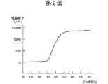
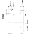
第1図に示すように、炭化物であるCr3C2(炭化クロム)と炭化物を形成しにくい材料であるCo(コバルト)とを混合した粉末を圧縮成形し、その後に電極強度を増すため加熱して電極を製作した場合、炭化物を形成しにくいCoの量を変化させることで厚膜の形成しやすさが変わっていく。第2図はこの様子を示したものである。電極を作製する際の粉末を圧縮成プレス圧は約100MPaであり、加熱温度は400℃から800℃の範囲形で変化させた。Cr3C2(炭化クロム)が多いほど加熱温度は高くし、Co(コバルト)が多いほど温度を低くした。これは、Cr3C2(炭化クロム)が多い場合には製作した電極が脆くなりやすく低い温度で加熱してもすぐに崩れてしまうのに対し、Co(コバルト)が多い場合には加熱温度が低くても電極の強度が強くなりやすかったためである。プレスの際には成形性をよくするためにプレスする粉末に少量(重量で2%から3%)のワックスを混合した。ワックスは加熱の際に除去される。Cr3C2(炭化クロム)は粒径3μm〜6μm程度の粉末を使用し、Coは粒径4μm〜6μm程度の粉末を使用した。ベースとなる材質はCr3C2(炭化クロム)である。使用した放電のパルスは第3図に示すような波形であり、パルス条件は、ピーク電流値ie=10A、放電持続時間(放電パルス幅)te=64μs、休止時間to=128μs、15mm×15mmの面積の電極において被膜を形成した。そして、処理時間は15分である。極性は、電極がマイナス、ワークがプラスの極性を使用した。第3図では、電極がマイナス、ワークがプラスの極性の場合に、縦軸上側になるように表示している。 As shown in FIG. 1, a powder obtained by mixing Cr 3 C 2 (chromium carbide), which is a carbide, and Co (cobalt), a material that is difficult to form a carbide, is compression-molded, and then heated to increase the electrode strength. When an electrode is manufactured, the ease of forming a thick film changes by changing the amount of Co that is difficult to form carbide. FIG. 2 shows this situation. The powder used to produce the electrode was compressed at a compression pressing pressure of about 100 MPa, and the heating temperature was changed in the range of 400 ° C to 800 ° C. The heating temperature was increased as the amount of Cr 3 C 2 (chromium carbide) was increased, and the temperature was decreased as the amount of Co (cobalt) was increased. This is because when the amount of Cr 3 C 2 (chromium carbide) is large, the manufactured electrode tends to become brittle and immediately collapses even when heated at a low temperature, whereas when the amount of Co (cobalt) is large, the heating temperature This is because the strength of the electrode was likely to increase even when the thickness was low. At the time of pressing, a small amount (2% to 3% by weight) of wax was mixed with the powder to be pressed in order to improve the moldability. The wax is removed on heating. Cr 3 C 2 (chromium carbide) used powder with a particle size of about 3 μm to 6 μm, and Co used powder with a particle size of about 4 μm to 6 μm. The base material is Cr 3 C 2 (chromium carbide). The discharge pulse used has a waveform as shown in FIG. 3. The pulse conditions are as follows: peak current value ie = 10 A, discharge duration (discharge pulse width) te = 64 μs, rest time to = 128 μs, 15 mm × 15 mm A coating was formed on the area electrode. The processing time is 15 minutes. The polarity was negative for the electrode and positive for the workpiece. In FIG. 3, when the electrode has a negative polarity and the workpiece has a positive polarity, the vertical axis is displayed on the upper side.
このようなパルス条件に基づいて被膜を形成した場合、製作した電極内にあって、Coが含有する重量%によってワーク上に形成される被膜の厚さが異なり、第2図によれば、Co含有量が低い場合には10μm程の膜厚であったものがCo含有量30体積%程度から次第に厚くなり、Co含有量50体積%を過ぎたころから10000μm近くにまで厚くなることを示している。 When a film is formed based on such a pulse condition, the thickness of the film formed on the workpiece varies depending on the weight percentage of Co in the manufactured electrode, and according to FIG. When the content is low, the film thickness of about 10 μm gradually increases from the Co content of about 30% by volume, and increases from around the Co content of 50% by volume to about 10,000 μm. Yes.
このことを更に詳細に述べる。上記のような条件に基づいてワーク上に被膜を形成した場合、電極内のCoが0%の場合、すなわち、Cr3C2(炭化クロム)が100重量%の場合には、形成できる被膜の厚さは10μm程度が限界であり、それ以上厚みを増すことはできない。また、炭化物を形成しにくい材料が電極内にない場合の処理時間に対する被膜の厚さの様子は第4図のようになる。第4図によれば、処理の初期は、被膜が時間とともに成長して厚くなり、あるところ(約5分/cm2)で飽和する。その後しばらく膜厚は成長しないが、ある時間(20分/cm2程度)以上処理を続けると今度は被膜の厚みが減少しはじめ、最後には被膜高さはマイナス、すなわち掘り込みに変わってしまう。ただし、掘り込んだ状態でも被膜は存在しており、その厚み自体は10μm程度であり、適切な時間で処理した状態とほとんど変わらない。したがって5分から20分の間での処理時間が適切と考えられる。 This will be described in more detail. When a film is formed on the workpiece based on the above conditions, when Co in the electrode is 0%, that is, when Cr 3 C 2 (chromium carbide) is 100% by weight, The limit is about 10 μm, and the thickness cannot be increased further. Moreover, the state of the thickness of the coating film with respect to the processing time when there is no material that hardly forms carbide in the electrode is as shown in FIG. According to FIG. 4, at the beginning of the treatment, the coating grows and thickens with time and saturates at some point (about 5 minutes / cm 2 ). After that, the film thickness does not grow for a while, but if the treatment is continued for a certain time (about 20 minutes / cm 2 ) or more, the thickness of the film starts to decrease and finally the film height becomes minus, that is, changes to digging. . However, the film is present even in the dug state, and the thickness itself is about 10 μm, which is almost the same as the state processed in an appropriate time. Therefore, the processing time between 5 minutes and 20 minutes is considered appropriate.
第2図に戻り、電極内に炭化しにくい材料であるCo量を増やすにしたがい厚くできるようになり、電極中におけるCo量が30体積%を超えると形成される被膜の厚さが厚くなり始め、40体積%を超えると安定して厚膜が形成しやすくなることが判明した。図2のグラフには、Co量30体積%程度から滑らかに膜厚が上昇するように記載しているが、これは、複数回の試験を行なった平均値であり、実際には、Co量が30体積%程度の場合には、厚く被膜が盛り上がらない場合があったり、厚く盛りあがった場合でも、被膜の強度が弱い、すなわち、金属片などで強く擦ると除去されてしまう場合などがあり、安定しない。より好ましくはCo量が50体積%を超えるとよい。このように被膜中に金属として残る材料を多くすることにより、炭化物になっていない金属成分を含む被膜を形成することができ、安定して厚膜が形成しやすくなる。ここでいう体積%は混合するそれぞれ粉末の重量をそれぞれの材料の密度で割った値の比率のことであり、粉末全体の材料の体積中においてその材料が占める体積の割合である。第5図に電極中におけるCoの含有量が70体積%の場合に形成した被膜の写真を示す。この写真は、厚膜の形成を例示するものである。第5図に示す写真においては2mm程度の厚膜が形成されている。この被膜は15分の処理時間で形成されたものであるが、処理時間を増せばさらに厚い被膜にすることができる。 Returning to FIG. 2, the thickness of the coating can be increased as the amount of Co, which is a material that is difficult to carbonize in the electrode, is increased, and when the amount of Co in the electrode exceeds 30% by volume, the thickness of the coating formed begins to increase. It has been found that when the amount exceeds 40% by volume, a thick film can be easily formed stably. The graph of FIG. 2 shows that the film thickness increases smoothly from about 30% by volume of Co, but this is an average value obtained by performing a plurality of tests. Is about 30% by volume, there are cases where the film does not swell thickly, or even when it swells thickly, the film strength is weak, that is, it may be removed by rubbing strongly with a metal piece, etc. Not stable. More preferably, the Co content exceeds 50% by volume. By increasing the amount of the material remaining as a metal in the coating in this way, a coating containing a metal component that is not carbide can be formed, and a thick film can be easily formed stably. The volume% here is a ratio of a value obtained by dividing the weight of each powder to be mixed by the density of each material, and is a ratio of the volume occupied by the material in the volume of the material of the whole powder. FIG. 5 shows a photograph of the film formed when the Co content in the electrode is 70% by volume. This photograph illustrates the formation of a thick film. In the photograph shown in FIG. 5, a thick film of about 2 mm is formed. This film is formed in a processing time of 15 minutes, but if the processing time is increased, a thicker film can be formed.
このようにして、電極内にCo等の炭化しにくい材料あるいは炭化しない材料を40体積%以上含有する電極を用いることによって、放電表面処理によりワーク表面に安定して厚い被膜を形成することができる。 In this way, by using an electrode containing 40% by volume or more of a material that is difficult to carbonize or not carbonized, such as Co, in the electrode, a thick film can be stably formed on the workpiece surface by discharge surface treatment. .
上記においては、炭化物を形成しにくい材料としてCo(コバルト)を用いた場合について説明したが、Ni(ニッケル)、Fe(鉄)なども同様の結果を得られる材料であり、本発明に用いて好適である。 In the above description, the case where Co (cobalt) is used as a material that hardly forms carbides has been described. However, Ni (nickel), Fe (iron), and the like are materials that can obtain similar results, and are used in the present invention. Is preferred.
なお、ここでいう厚膜とは、組織の内部(パルス状の放電により形成する被膜であるため、最表面は面粗さが悪く一見光沢がないように見える)が金属光沢を持つような緻密な被膜のことである。Co(コバルト)のような炭化物を形成しにくい材料が少ない場合でも、電極の強度を弱くすると付着物は盛り上がることがある。しかし、このような付着物は緻密な被膜ではなく、金属片などで擦ると容易に除去できるようなものである。前述の特許文献1などに記載されている堆積層は、このような緻密ではない被膜であり、金属片などで擦ると容易に除去できるものである。
The thick film here means a dense structure in which the inside of the tissue (which is a film formed by pulsed discharge, so that the outermost surface has poor surface roughness and does not appear glossy) has a metallic luster. It is a simple film. Even when there are few materials such as Co (cobalt) that are difficult to form carbides, deposits may rise when the strength of the electrode is reduced. However, such a deposit is not a dense film, but can be easily removed by rubbing with a metal piece or the like. The deposited layer described in the above-mentioned
また、上記の説明においては、Cr3C2(炭化クロム)およびCo粉末を圧縮成形して加熱し電極を形成した場合について説明したが、圧縮成形した圧粉体を電極として使用してもよい場合もある。しかし、緻密な厚膜を形成するためには、電極の硬さが硬すぎても軟らかすぎてもよくなく、適切な硬さが必要である。一般的には、加熱処理が必要である。圧粉体を加熱することは成形の維持や固形化につながる。電極の硬さは、電極材料の粉末の結合の強さに層間があり、放電による電極材料のワーク側への供給量に関係している。電極の硬さが硬い場合には、電極材料の結合が強いため、放電が発生しても少量の電極材料しか放出されず、十分に被膜形成ができない。逆に電極の硬さが低い場合には、電極材料の結合が弱いため、放電が発生すると、大量の材料が供給され、この量が多すぎる場合には、十分放電パルスのエネルギーで溶融させることができず、緻密な被膜を形成できなくなる。同じ原料の粉末を使用した場合、電極の硬さ、すなわち、電極の材料の結合状態に影響をあたえるパラメータが、プレス圧と加熱温度である。本実施例では、プレス圧の例として約100MPaを使用したが、このプレスをされに上げると加熱温度を低くしても同じような硬さが得られる。逆に、プレス圧を低くすると、加熱温度を高めに設定する必要があることがわかった。この事実は、本実施例だけでなく、本発明中の他の実施例にも当てはまるものである。 In the above description, the case where Cr 3 C 2 (chromium carbide) and Co powders are compression-molded and heated to form an electrode has been described. However, a compression-molded green compact may be used as the electrode. In some cases. However, in order to form a dense thick film, the electrode may not be too hard or too soft, and an appropriate hardness is required. In general, heat treatment is required. Heating the green compact leads to maintenance and solidification of the molding. The hardness of the electrode is related to the amount of supply of the electrode material to the work side by electric discharge, because there is an interlayer in the bonding strength of the powder of the electrode material. When the electrode is hard, the bonding of the electrode material is strong, so that only a small amount of the electrode material is released even when a discharge occurs, and a film cannot be formed sufficiently. Conversely, when the electrode hardness is low, the bonding of the electrode material is weak, so when a discharge occurs, a large amount of material is supplied, and if this amount is too large, it should be melted sufficiently with the energy of the discharge pulse. It is impossible to form a dense film. When the same raw material powder is used, parameters affecting the hardness of the electrode, that is, the bonding state of the material of the electrode, are the pressing pressure and the heating temperature. In this example, about 100 MPa was used as an example of the press pressure, but when this press is raised, the same hardness can be obtained even if the heating temperature is lowered. Conversely, it was found that when the press pressure is lowered, the heating temperature needs to be set higher. This fact applies not only to this embodiment but also to other embodiments in the present invention.
また、本実施例では、放電条件の例として1つの条件での試験結果を示したが、被膜の厚さなど異なるが、他の条件でも、同様の結果が得られることはいうまでない。この事実も、本実施例だけでなく、本発明中の他の実施例にも当てはまるものである。 In this embodiment, the test result under one condition is shown as an example of the discharge condition. However, it is needless to say that the same result can be obtained under other conditions although the thickness of the film is different. This fact applies not only to this embodiment but also to other embodiments of the present invention.
第6図は、本発明の第1の実施の形態にかかる放電表面処理装置を示す概略構成図である。第6図に示すように、本実施の形態にかかる放電表面処理装置は、上述した放電表面処理用電極であり、炭化物を形成しないもしくは形成しにくい金属材料を40体積%以上含んだ粉末を圧縮成形した圧粉体、またはこの圧粉体を加熱処理した圧粉体からなる電極203と、加工液205である油と、電極203とワーク204とを加工液中に浸漬させる、または電極203とワーク204との間に加工液205を供給する加工液供給装置208と、電極203とワーク204との間に電圧を印加してパルス状の放電を発生させる放電表面処理用電源206とを備えて構成される。
FIG. 6 is a schematic configuration diagram showing the discharge surface treatment apparatus according to the first embodiment of the present invention. As shown in FIG. 6, the discharge surface treatment apparatus according to the present embodiment is a discharge surface treatment electrode as described above, and compresses a powder containing 40% by volume or more of a metal material that does not form carbide or is difficult to form. An
ここで、電極203は例えばCr3C2(炭化クロム)粉末201とCo(コバルト)粉末202とから構成されており、炭化物を形成しにくい材料であるCoを例えば70体積%含むものである。なお、電極203とワーク204の相対位置を制御する駆動装置などの本発明に直接関係のない部材は記載を省略している。
Here, the
この放電表面処理装置によりワーク表面に被膜を形成するには、電極203とワーク204とを加工液205の中で対向配置し、加工液中において放電表面処理用電源206から電極203とワーク204との間にパルス状の放電を発生させ、その放電エネルギにより電極材料の被膜をワーク表面に形成しあるいは放電エネルギにより電極材料が反応した物質の被膜をワーク表面に形成する。極性は、電極側がマイナス、ワーク側がプラスの極性を使用する。放電のアーク柱207は第6図に示すように電極203とワーク204との間に発生する。
In order to form a film on the surface of the workpiece by this discharge surface treatment apparatus, the
以上のような放電表面処理装置を用いてワーク204に被膜を形成することにより、液中パルス放電処理により安定してワーク表面に厚膜の被膜を形成することができる。
By forming a film on the
実施の形態2
第7図は、この発明の実施の形態2にかかる放電表面処理用電極およびその製造方法の概念を示す断面図である。第7図において、金型の上パンチ703、金型の下パンチ704、金型のダイ705で囲まれた空間には、Ti(チタン)粉末701及びCo(コバルト)粉末702からなる混合粉末が充填される。そして、この混合粉末を圧縮成形することにより圧粉体を形成する。放電表面処理加工に当たっては、この圧粉体が放電電極とされる。電極を作製する際の粉末を圧縮成プレス圧は約100MPaであり、加熱温度は400℃から800℃の範囲形で変化させた。
Embodiment 2
FIG. 7 is a cross-sectional view showing the concept of the discharge surface treatment electrode and the method for manufacturing the same according to the second embodiment of the present invention. In FIG. 7, a mixed powder composed of Ti (titanium) powder 701 and Co (cobalt) powder 702 is placed in a space surrounded by the
上述した実施の形態1では、炭化物であるCr3C2(炭化クロム)粉末と金属であるCo(コバルト)粉末とを混合して製造した電極での被膜形成の特徴について述べたが、本実施例では、金属であるTi(チタン)粉末とCo(コバルト)粉末とを混合して電極を製造した場合について説明する。Ti(チタン)とCo(コバルト)はともに金属であるが、違いは、Ti(チタン)が活性な材料であり加工液である油中での放電の雰囲気下で炭化物であるTiC(炭化チタン)に極めてなり易い材料であるのに対し、Co(コバルト)は炭化物を形成しにくい材料であるという点である。 In the first embodiment described above, the characteristics of film formation with an electrode manufactured by mixing Cr 3 C 2 (chromium carbide) powder as a carbide and Co (cobalt) powder as a metal have been described. In the example, a case where an electrode is manufactured by mixing Ti (titanium) powder and Co (cobalt) powder, which are metals, will be described. Ti (titanium) and Co (cobalt) are both metals, but the difference is that Ti (titanium) is an active material and TiC (titanium carbide) which is a carbide in the atmosphere of electric discharge in oil as a working fluid. Co (cobalt) is a material that hardly forms carbides.
実施の形態2では実施の形態1の場合と同様に電極中におけるTi(チタン)粉末の含有率をTi(チタン)粉末100体積%、すなわち電極内のCoが0体積%の場合からCo(コバルト)粉末の含有量を順次増やし、膜の成形の状態がどのようになるか調べた。ここで、Ti(チタン)粉末は、粒径3μmから4μm程度の粉末を使用し、Co(コバルト)粉末は粒径粒径4μm〜6μm程度の粉末を使用した。Ti(チタン)は粘りのある材料であるため微粉の製造が困難であるので、脆い材料であるTiH2(水素化チタン)を粒径3μmから4μm程度にボールミルで粉砕し、その粉末を使用して圧縮成形した後、加熱して水素を放出させてTiの粉末とした。 In the second embodiment, as in the first embodiment, the content of Ti (titanium) powder in the electrode is changed to 100% by volume of Ti (titanium) powder, that is, Co (cobalt) is changed from the case where Co in the electrode is 0% by volume. ) The powder content was gradually increased, and the state of film formation was examined. Here, as the Ti (titanium) powder, a powder having a particle size of about 3 μm to 4 μm was used, and as the Co (cobalt) powder, a powder having a particle size of about 4 μm to 6 μm was used. Since Ti (titanium) is a sticky material, it is difficult to produce fine powder. TiH 2 (titanium hydride), which is a brittle material, is pulverized with a ball mill to a particle size of 3 μm to 4 μm, and the powder is used. After compression molding, the mixture was heated to release hydrogen to obtain Ti powder.
電極材料が、Ti(チタン)100体積%の場合には、被膜はTiC(炭化チタン)となり、膜厚は10μm程度であった。しかし、炭化しにくい材料であるCoの含有量を増やすにしたがい厚い被膜が形成できるようになり、電極中におけるCoの含有量が40体積%を超えると安定して厚膜が形成しやすくなることが判明した。そして、電極中におけるCoの含有量が50体積%をこえると十分な厚みの厚膜を形成できるため好ましいことが判明した。この結果は、実施の形態1で示した結果とほぼ同じ結果である。これは、電極中に含まれるTi(チタン)は、加工液である油中での放電の雰囲気では炭化物であるTiC(炭化チタン)になってしまい初めから炭化物を混合するのと同じような結果になるためであると推察される。実際に被膜の成分をX線回折により分析すると、TiC(炭化チタン)の存在を示すピークは観察されるが、Ti(チタン)の存在を示すピークは観察されなかった。 When the electrode material was 100% by volume of Ti (titanium), the film was TiC (titanium carbide), and the film thickness was about 10 μm. However, a thick film can be formed as the content of Co, which is a material that is not easily carbonized, is increased. If the Co content in the electrode exceeds 40% by volume, a thick film can be easily formed stably. There was found. It has been found that it is preferable that the Co content in the electrode exceeds 50% by volume because a sufficiently thick film can be formed. This result is almost the same as the result shown in the first embodiment. This is because Ti (titanium) contained in the electrode becomes TiC (titanium carbide) which is a carbide in the atmosphere of discharge in oil as a working fluid, and the result is similar to mixing carbide from the beginning. It is guessed that it is to become. When the components of the film were actually analyzed by X-ray diffraction, a peak indicating the presence of TiC (titanium carbide) was observed, but a peak indicating the presence of Ti (titanium) was not observed.
したがって、Ti(チタン)粉末とCo(コバルト)粉末とを混合して電極を製造した場合についても、電極内に炭化しにくい材料あるいは炭化しない材料としてのCo(コバルト)粉末を40体積%以上含有させた電極とすることによって、放電表面処理によりワーク表面に安定して厚い被膜を形成することができる。 Therefore, even when an electrode is manufactured by mixing Ti (titanium) powder and Co (cobalt) powder, the electrode contains 40 vol% or more of Co (cobalt) powder as a material that is not easily carbonized or is not carbonized. By forming the electrode, a thick film can be stably formed on the workpiece surface by the discharge surface treatment.
なお、本実施の形態においてはTi(チタン)粉末と混合して電極を構成する炭化物を形成しにくい材料としてCo(コバルト)を用いた場合を例に挙げたが、Ni(ニッケル)、Fe(鉄)なども同様の結果を得られる材料であり、本発明に用いて好適である。 In this embodiment, Co (cobalt) is used as an example of a material that hardly mixes with Ti (titanium) powder to form a carbide constituting the electrode. However, Ni (nickel), Fe ( Iron) is a material that can obtain the same result, and is suitable for use in the present invention.
実施の形態3
第8図は、この発明の実施の形態3にかかる放電表面処理用電極およびその製造方法の概念を示す断面図である。第8図において、金型の上パンチ803、金型の下パンチ804、金型のダイ805で囲まれた空間には、Cr(クロム)粉末801及びCo(コバルト)粉末802からなる混合粉末が充填される。そして、この混合粉末を圧縮成形することにより圧粉体を形成する。放電表面処理加工に当たっては、この圧粉体が放電電極とされる。電極を作製する際の粉末を圧縮成プレス圧は約100MPaであり、加熱温度は400℃から800℃の範囲形で変化させた。
Embodiment 3
FIG. 8 is a cross-sectional view showing the concept of the discharge surface treatment electrode and the method of manufacturing the same according to the third embodiment of the present invention. In FIG. 8, in a space surrounded by the
実施例2では、炭化物を形成しやすい金属であるTi(チタン)粉末と炭化しにくい材料であるCo(コバルト)粉末とを混合した電極での被膜形成の場合について説明したが、本実施例では、炭化物を形成する金属であるCr(クロム)の粉末と炭化物を形成しにくい材料であるCo(コバルト)の粉末とを混合して電極を製造した場合について説明する。 In Example 2, the case of forming a film with an electrode in which Ti (titanium) powder, which is a metal that easily forms carbides, and Co (cobalt) powder, which is a material that does not easily carbonize, has been described. In this example, A case will be described in which an electrode is manufactured by mixing Cr (chromium) powder, which is a metal forming carbide, and Co (cobalt) powder, which is a material difficult to form carbide.
実施の形態3では実施の形態1の場合と同様に電極中におけるCr(クロム)粉末の含有率をCr(クロム)粉末100体積%、すなわち電極内のCoが0体積%の場合からCo(コバルト)粉末の含有量を順次増やし、膜の成形の状態がどのようになるか調べた。ここで、Cr(クロム)粉末は粒径3μmから4μm程度の粉末を使用し、Co(コバルト)粉末は粒径粒径4μm〜6μm程度の粉末を使用した。 In the third embodiment, as in the first embodiment, the Cr (chromium) powder content in the electrode is changed to 100 vol% of Cr (chromium) powder, that is, Co (cobalt) is changed from the case where Co in the electrode is 0 vol% ) The powder content was gradually increased, and the state of film formation was examined. Here, as the Cr (chromium) powder, a powder having a particle size of about 3 μm to 4 μm was used, and as the Co (cobalt) powder, a powder having a particle size of about 4 μm to 6 μm was used.
電極材料が、Cr(クロム)100体積%の場合には、被膜の膜厚は10μm程度であった。しかし、被膜成分をX線回折により分析すると、Cr3C2(炭化クロム)の存在を示すピークと、Cr(クロム)の存在を示すピークが観察された。すなわち、Cr(クロム)は炭化し易い材料ではあるがTi(チタン)のような材料に比べると炭化しやすさは低く、電極中にCr(クロム)が含まれている場合にはその一部が炭化物になり、一部は金属のCr(クロム)のまま被膜となるということになる。 When the electrode material was 100% by volume of Cr (chromium), the film thickness was about 10 μm. However, when the film component was analyzed by X-ray diffraction, a peak indicating the presence of Cr 3 C 2 (chromium carbide) and a peak indicating the presence of Cr (chromium) were observed. That is, although Cr (chromium) is a material that is easily carbonized, it is less easily carbonized than a material such as Ti (titanium), and a part of the electrode contains Cr (chromium). Becomes a carbide, and a part of the film remains a metallic Cr (chromium).
電極成分としてCr(クロム)を使用する場合にも、炭化しにくい材料であるCoの含有量を増やすにしたがい被膜は厚くできるようになることが判明した。但し、その割合は実施の形態1および実施の形態2の場合のように電極成分に炭化物が含まれている場合や炭化物に極めてなり易い材料が含まれている場合よりも少なくてもよく、電極中におけるCoの含有量が20体積%を超えるころから厚膜が形成しやすくなることが判明した。 Even when Cr (chromium) is used as an electrode component, it has been found that the coating can be made thicker as the content of Co, which is a material that is not easily carbonized, is increased. However, the ratio may be smaller than that in the case where the electrode component contains carbide or the material that is extremely likely to become carbide as in the case of the first and second embodiments. It has been found that a thick film can be easily formed when the Co content in the medium exceeds 20% by volume.
Coの量を変化させた場合の被膜の厚みの変化を第9図に示す。使用した放電のパルス条件は、実施例1および実施例2の場合と同じで、ピーク電流値ie=10A、放電持続時間(放電パルス幅)te=64μs、休止時間to=128μsであり、15mm×15mmの面積の電極で被膜を形成した。極性は、電極がマイナス、ワークがプラスの極性を使用した。処理時間は15分である。 FIG. 9 shows the change in the thickness of the film when the amount of Co is changed. The discharge pulse conditions used were the same as those in Example 1 and Example 2, peak current value ie = 10 A, discharge duration (discharge pulse width) te = 64 μs, pause time to = 128 μs, 15 mm × A film was formed with an electrode having an area of 15 mm. The polarity was negative for the electrode and positive for the workpiece. Processing time is 15 minutes.
以上のように、炭化物を形成し易い材料の中にも炭化のし易さには差異があり、炭化しにくい材料ほどより厚膜を形成しやすい傾向がある。これは、厚膜を形成する条件が、被膜となった材料中に炭化物にならず金属のまま存在する材料の割合が所定量あることであるためと推察される。実施の形態1から実施の形態3に示した結果などから考察すると、被膜中に金属として残る材料の割合が体積で30%程度以上存在することが緻密な厚膜を形成するための必要条件と考えられる。 As described above, there is a difference in easiness of carbonization among materials that easily form carbides, and a material that is hard to carbonize tends to form a thicker film. This is presumably because the condition for forming the thick film is that there is a predetermined amount of the material that does not become carbides but remains in the metal in the coated material. Considering the results shown in the first to third embodiments, the necessary condition for forming a dense thick film is that the ratio of the material remaining as metal in the coating is about 30% or more by volume. Conceivable.
また、加工液である油中での放電の雰囲気での金属材料の炭化のしやすさについては、明確なデータはないが、上記において説明したような実験データなどから考えるとエリンガム図に示されている炭化する場合に必要なエネルギの大きさが参考になると考えられる。エリンガム図によると、Ti(チタン)はきわめて炭化しやすいことが示されており、Cr(クロム)はTiに比べると炭化しにくいといえる。炭化物を形成し易い材料のなかでも、TiやMo(モリブデン)は炭化しやすく、Cr(クロム)やSi(シリコン)などは比較的炭化しにくい材料であると考えられ、これらは実際の実験結果ともよく合致する結果である。 In addition, there is no clear data on the ease of carbonization of metal materials in the discharge atmosphere in oil as the working fluid, but it is shown in the Ellingham diagram when considered from the experimental data described above. The amount of energy required for carbonization is considered to be helpful. The Ellingham diagram shows that Ti (titanium) is very easily carbonized, and it can be said that Cr (chromium) is harder to carbonize than Ti. Among materials that easily form carbides, Ti and Mo (molybdenum) are easily carbonized, and Cr (chromium) and Si (silicon) are considered to be relatively difficult to carbonize. The results are in good agreement.
上述したように、Cr(クロム)粉末とCo(コバルト)粉末とを混合して電極を製造した場合についても、電極内に炭化しにくい材料あるいは炭化しない材料としてのCo(コバルト)粉末を40体積%以上含有させた電極とすることによって、放電表面処理によりワーク表面に安定して厚い被膜を形成することができる。そして、この場合には特に電極中にCoを20体積%以上含有させた電極であればワーク表面に安定して厚い被膜を形成することができる。 As described above, even when an electrode is manufactured by mixing Cr (chromium) powder and Co (cobalt) powder, 40 vol. Of Co (cobalt) powder as a material that is not easily carbonized or is not carbonized in the electrode. By making the electrode contained at least%, a thick film can be stably formed on the workpiece surface by the discharge surface treatment. In this case, a thick film can be stably formed on the surface of the work, particularly if the electrode contains 20% by volume or more of Co.
なお、本実施の形態においてはCr(クロム)粉末と混合して電極を構成する炭化物を形成しにくい材料としてCo(コバルト)を用いた場合を例に挙げたが、Ni(ニッケル)、Fe(鉄)なども同様の結果を得られる材料であり、本発明に用いて好適である。 In this embodiment, Co (cobalt) is used as an example of a material that is difficult to form carbides constituting the electrode by mixing with Cr (chromium) powder. However, Ni (nickel), Fe ( Iron) is a material that can obtain the same result, and is suitable for use in the present invention.
実施の形態4
第10図は、この発明の実施の形態4にかかる放電表面処理用電極およびその製造方法の概念を示す断面図である。第10図において、金型の上パンチ1005、金型の下パンチ1006、金型のダイ1007で囲まれた空間には、Mo(モリブデン)粉末1001、Cr(クロム)粉末1002、Si(シリコン)粉末1003及びCo(コバルト)粉末1004からなる混合粉末が充填される。粉末の配合比率は、Mo(モリブデン)28重量%、Cr(クロム)17重量%、Si(シリコン)3重量%、Co(コバルト)52重量%である。この場合のCo(コバルト)の体積%は約50%である。そして、この混合粉末を圧縮成形することにより圧粉体を形成する。放電表面処理加工に当たっては、この圧粉体が放電電極とされる。
Embodiment 4
FIG. 10 is a sectional view showing the concept of a discharge surface treatment electrode and a method for manufacturing the same according to a fourth embodiment of the present invention. In FIG. 10, in a space surrounded by the
Mo(モリブデン)28重量%、Cr(クロム)17重量%、Si(シリコン)3重量%、Co(コバルト)52重量%の比率は、高温環境下での耐磨耗のための材料として使用される組み合わせである。このような比率で配合された電極は、材料の持つ硬さと、高温環境下でCr(クロム)が酸化してできるCr2O3(酸化クロム)が潤滑性を発揮することから耐磨耗の効果を発揮する。 The ratio of 28 wt% Mo (molybdenum), 17 wt% Cr (chromium), 3 wt% Si (silicon) and 52 wt% Co (cobalt) is used as a material for wear resistance in high temperature environments. It is a combination. The electrode blended in such a ratio is resistant to wear because the hardness of the material and Cr 2 O 3 (chromium oxide) formed by oxidation of Cr (chromium) under high temperature environment exhibit lubricity. Demonstrate the effect.
電極を作製する際の粉末を圧縮成形するプレス圧は約100MPa、加熱温度は600℃から800℃の範囲とした。プレスの際には、成形性をよくするために、プレスする粉末に少量(重量で2%から3%)のワックスを混合した。ワックスは加熱の際に除去される。粉末は各材料とも粒径2μm〜6μm程度の粉末を使用した。使用した放電のパルス条件は、ピーク電流値ie=10A、放電持続時間(放電パルス幅)te=64μs、休止時間to=128μs、15mm×15mmの面積の電極で被膜を形成した。極性は、電極がマイナス、ワークがプラスの極性を使用した。 The press pressure for compressing and molding the powder in producing the electrode was about 100 MPa, and the heating temperature was in the range of 600 ° C to 800 ° C. At the time of pressing, in order to improve moldability, a small amount (2% to 3% by weight) of wax was mixed with the powder to be pressed. The wax is removed on heating. As the powder, a powder having a particle size of about 2 μm to 6 μm was used for each material. The discharge pulse conditions used were a peak current value ie = 10 A, a discharge duration (discharge pulse width) te = 64 μs, a rest time to = 128 μs, and an electrode having an area of 15 mm × 15 mm. The polarity was negative for the electrode and positive for the workpiece.
以上のようにして作製した電極を用いることにより第6図と同様の放電表面処理装置を構成することができる。そして、該放電表面処理装置により液中パルス放電処理によりワーク表面に被膜を形成したところ、ワーク材料に加工液である油中でのパルス放電による歪を生じることなく厚い被膜を形成することができた。また、形成された被膜が高温環境下で耐磨耗性を発揮することも確認され、良質の厚膜を形成することができた。 By using the electrode produced as described above, a discharge surface treatment apparatus similar to that shown in FIG. 6 can be constructed. When a coating film is formed on the workpiece surface by the pulse discharge treatment in the liquid using the discharge surface treatment apparatus, a thick coating film can be formed on the workpiece material without causing distortion due to the pulse discharge in the oil that is the working fluid. It was. In addition, it was confirmed that the formed film exhibited wear resistance in a high temperature environment, and a high-quality thick film could be formed.
上述したような比率で材料を混合して作製した電極を用いて液中パルス放電処理によりワーク表面に被膜を形成することで耐摩耗性等の各種機能を有する被膜が得られるが、このような材料としては、他に「Cr(クロム)25重量%、Ni(ニッケル)10重量%、W(タングステン)7重量%、Co(コバルト)残」、または「Cr(クロム)20重量%、Ni(ニッケル)10重量%、W(タングステン)15重量%、Co(コバルト)残」などのステライトなどが挙げられる。ステライトは耐蝕性、高温硬さに優れるため、通常これらの性質の必要な部分に溶接などによりコーティング処理がなされる材料であり、耐蝕性、高温硬さを要する際のコーティング処理に好適である。 A film having various functions such as wear resistance can be obtained by forming a film on the work surface by pulse discharge treatment in liquid using an electrode prepared by mixing materials in the above-described ratio. Other materials include “Cr (chromium) 25 wt%, Ni (nickel) 10 wt%, W (tungsten) 7 wt%, Co (cobalt) residue”, or “Cr (chromium) 20 wt%, Ni ( Nickel), 10% by weight, W (tungsten) 15% by weight, and Co (cobalt) residue ”. Since stellite is excellent in corrosion resistance and high temperature hardness, it is a material that is usually subjected to a coating treatment by welding or the like on a portion requiring these properties, and is suitable for a coating treatment when corrosion resistance and high temperature hardness are required.
また、「Cr(クロム)15重量%、Fe(鉄)8重量%、Ni(ニッケル)残」、「Cr(クロム)21重量%、Mo(モリブデン)9重量%、Ta(タンタル)4重量%、Ni(ニッケル)残」、「Cr(クロム)19重量%、Ni(ニッケル)53重量%、Mo(モリブデン)3重量%、(Cb+Ta)5重量%、Ti(チタン)0.8重量%、Al(アルミ)0.6重量%、Fe(鉄)残」などのニッケル基の配合の材料は耐熱性を発揮する材料であり、耐熱性を要する際のコーティング処理に好適である。 Also, “Cr (chromium) 15 wt%, Fe (iron) 8 wt%, Ni (nickel) residue”, “Cr (chromium) 21 wt%, Mo (molybdenum) 9 wt%, Ta (tantalum) 4 wt% , Ni (nickel) residue ”,“ Cr (chromium) 19 wt%, Ni (nickel) 53 wt%, Mo (molybdenum) 3 wt%, (Cb + Ta) 5 wt%, Ti (titanium) 0.8 wt%, Nickel-based materials such as “Al (aluminum) 0.6 wt%, Fe (iron) residue” are materials that exhibit heat resistance, and are suitable for coating processing when heat resistance is required.
実施の形態5
第11図は、この発明の実施の形態5にかかる放電表面処理用電極およびその製造方法の概念を示す断面図である。第11図において、金型の上パンチ1103、金型の下パンチ1104、金型のダイ1105で囲まれた空間には、ステライト合金粉末(Co、Cr、Niの合金の粉末)1101が充填される。そして、この混合粉末を圧縮成形することにより圧粉体を形成する。放電表面処理加工に当たっては、この圧粉体が放電電極とされる。
Embodiment 5
FIG. 11 is a sectional view showing the concept of a discharge surface treatment electrode and a method for manufacturing the same according to a fifth embodiment of the present invention. In FIG. 11, the space surrounded by the
粉末1101は、Co(コバルト)、Cr(クロム)、Ni(ニッケル)などを所定の合金比率で混合して作った合金(ステライト)を粉末にしたものである。粉末にする方法は、例えばアトマイズ法や、合金をミルなどにより粉砕する方法が挙げられる。いずれの方法においても粉末粒一つ一つが合金(第11図の場合はステライト)になっている。合金粉末をダイ1105とパンチ1103、1104により圧縮成形する。場合によっては、電極の強度を増すためにその後加熱処理を行なっても良い。ここでは、「Cr(クロム)20重量%、Ni(ニッケル)10重量%、W(タングステン)15重量%、Co(コバルト)残」の合金比率の合金の粉末を使用した。この場合のCo(コバルト)の体積%は40%以上である。
The powder 1101 is a powder made of an alloy (sterite) made by mixing Co (cobalt), Cr (chromium), Ni (nickel) or the like at a predetermined alloy ratio. Examples of the method for forming the powder include an atomizing method and a method of pulverizing the alloy with a mill. In either method, each powder particle is an alloy (in the case of FIG. 11, stellite). The alloy powder is compression molded by a
粉末を圧縮成形するプレス圧は約100MPa、加熱温度は600℃から800℃の範囲とした。プレスの際には、成形性をよくするために、プレスする粉末に少量(重量で2%から3%)のワックスを混合した。ワックスは加熱の際に除去される。粉末は各材料とも粒径2μm〜6μm程度の粉末を使用した。使用した放電のパルス条件は、ピーク電流値ie=10A、放電持続時間(放電パルス幅)te=64μs、休止時間to=128μs、15mm×15mmの面積の電極で被膜を形成した。極性は、電極がマイナス、ワークがプラスの極性を使用した。 The press pressure for compressing the powder was about 100 MPa, and the heating temperature was in the range of 600 ° C to 800 ° C. At the time of pressing, in order to improve moldability, a small amount (2% to 3% by weight) of wax was mixed with the powder to be pressed. The wax is removed on heating. As the powder, a powder having a particle size of about 2 μm to 6 μm was used for each material. The discharge pulse conditions used were a peak current value ie = 10 A, a discharge duration (discharge pulse width) te = 64 μs, a rest time to = 128 μs, and an electrode having an area of 15 mm × 15 mm. The polarity was negative for the electrode and positive for the workpiece.
以上のようにして作製した電極を用いて構成した本実施の形態にかかる放電表面処理装置を示す概略構成図を第12図に示す。第12図に示すように放電表面処理装置は、上述した合金比率の合金粉末からなる電極1202と、加工液1204である油と、電極1202とワーク1203とを加工液中に浸漬させる、または電極1202とワーク1203との間に加工液1204を供給する加工液供給装置1208と、電極1202とワーク1203との間に電圧を印加してパルス状の放電を発生させる放電表面処理用電源1205とを備えて構成されている。電極1202は合金粉末1201からできている。なお、放電表面処理用電源1205とワーク1203の相対位置を制御する駆動装置などの本発明に直接関係のない部材は記載を省略している。
FIG. 12 shows a schematic configuration diagram illustrating the discharge surface treatment apparatus according to the present embodiment configured using the electrodes manufactured as described above. As shown in FIG. 12, the discharge surface treatment apparatus immerses the
この放電表面処理装置によりワーク表面に被膜を形成するには、電極1202とワーク1203とを加工液1204の中で対向配置し、加工液中において放電表面処理用電源1205から電極1202とワーク1203との間にパルス状の放電を発生させ、その放電エネルギにより電極材料の被膜をワーク表面に形成しあるいは放電エネルギにより電極材料が反応した物質の被膜をワーク表面に形成する。極性は、電極側がマイナス、ワーク側がプラスの極性を使用する。第12図に示すように放電のアーク柱1206は電極1202とワーク1203との間に発生する。
In order to form a coating film on the workpiece surface with this discharge surface treatment apparatus, the
放電毎に電極材料がワーク側に供給される。電極材料は粉末から成っているが合金を粉末化したものを使用しているので材質が均一であり、電極1202に供給される場合にも材質のばらつきがない。その結果、電極材料の材質の不均一に起因した成分のばらつきのない良質の被膜を形成することができる。
The electrode material is supplied to the workpiece side for each discharge. Although the electrode material is made of powder, it is made of a powdered alloy, so the material is uniform, and even when supplied to the
各材料の粉末を混合して所定の組成の電極を製造する場合には、粉末の混合のばらつきにより一定した材料の性能が得られないという問題が生じうる。本発明者らの研究によると、各材料の粉末を混合して所定の組成の電極を製造する場合には複数の粉末を混合するため完全に均一に混合するということが極めて困難であり、電極の個体間のばらつき、あるいは、1つの電極の中でも場所によるばらつきが発生しうることが判明した。これは炭化物を形成しやすい材料を含んだ電極の場合には影響が大きい。例えば、後述する合金のようにMo(モリブデン)やTi(チタン)など炭化しやすい材料が偏在した場合には、その部分のみ厚膜を形成しにくくなってしまう。被膜中の成分とともに、膜厚も均一でなくなってしまうという問題がある。 When an electrode having a predetermined composition is manufactured by mixing powders of respective materials, there may be a problem that a constant material performance cannot be obtained due to variations in mixing of the powders. According to the researches of the present inventors, it is extremely difficult to mix a plurality of powders completely and uniformly when an electrode having a predetermined composition is produced by mixing powders of respective materials. It has been found that variation among individuals or variation depending on location can occur within one electrode. This has a great effect in the case of an electrode containing a material that easily forms carbides. For example, when an easily carbonized material such as Mo (molybdenum) or Ti (titanium) is unevenly distributed like an alloy described later, it is difficult to form a thick film only at that portion. There is a problem that the film thickness is not uniform together with the components in the film.
しかしながら、本実施の形態に示したように複数の元素を所定の比率で合金化した合金材料の粉末を作り、その粉末から電極を製造することで、電極の成分上のばらつきをなくすことが可能となった。そして、該電極を用いて放電表面処理を行うことにより安定してワーク表面に厚膜の被膜を形成することが可能であり、形成した被膜の被膜成分も均一な状態にすることが可能となった。 However, as shown in the present embodiment, it is possible to eliminate variations in electrode components by making a powder of an alloy material in which a plurality of elements are alloyed at a predetermined ratio and manufacturing an electrode from the powder. It became. Then, by performing discharge surface treatment using the electrode, it is possible to stably form a thick film on the workpiece surface, and the film component of the formed film can be made uniform. It was.
したがって、以上のような電極を用いた放電表面処理装置を用いてワーク1203に被膜を形成することにより、液中パルス放電処理により安定してワーク表面に被膜成分も均一な厚膜を形成することができる。
Therefore, by forming a film on the
上記においては、「Cr(クロム)20重量%、Ni(ニッケル)10重量%、W(タングステン)15重量%、Co(コバルト)残」の合金比率の合金を粉末化した材料を使用したが、粉末化する合金は他の配合の合金でももちろんよく、例えば、「Cr(クロム)25重量%、Ni(ニッケル)10重量%、W(タングステン)7重量%、Co(コバルト)残」の合金比率の合金を用いることもできる。また、「Mo(モリブデン)28重量%、Cr(クロム)17重量%、Si(シリコン)3重量%、Co(コバルト)残」「Cr(クロム)15重量%、Fe(鉄)8重量%、Ni(ニッケル)残」、「Cr(クロム)21重量%、Mo(モリブデン)9重量%、Ta(タンタル)4重量%、Ni(ニッケル)残」、「Cr(クロム)19重量%、Ni(ニッケル)53重量%、Mo(モリブデン)3重量%、(Cb+Ta)5重量%、Ti(チタン)0.8重量%、Al(アルミ)0.6重量%、Fe(鉄)残」の合金比率の合金でもよい。但し、合金の合金比率が異なると材料の硬さなどの性質が異なるため、電極の成形性・被膜の状態に多少の差異が生じる。 In the above, a material obtained by pulverizing an alloy having an alloy ratio of “Cr (chromium) 20 wt%, Ni (nickel) 10 wt%, W (tungsten) 15 wt%, Co (cobalt) residue” is used. Of course, the alloy to be powdered may be an alloy of other composition, for example, an alloy ratio of “Cr (chromium) 25 wt%, Ni (nickel) 10 wt%, W (tungsten) 7 wt%, Co (cobalt) residue”. These alloys can also be used. “Mo (molybdenum) 28 wt%, Cr (chromium) 17 wt%, Si (silicon) 3 wt%, Co (cobalt) residue” “Cr (chromium) 15 wt%, Fe (iron) 8 wt%, "Ni (nickel) residue", "Cr (chromium) 21 wt%, Mo (molybdenum) 9 wt%, Ta (tantalum) 4 wt%, Ni (nickel) residue", "Cr (chromium) 19 wt%, Ni ( (Nickel) 53 wt%, Mo (molybdenum) 3 wt%, (Cb + Ta) 5 wt%, Ti (titanium) 0.8 wt%, Al (aluminum) 0.6 wt%, Fe (iron) balance "alloy ratio An alloy of may be used. However, since the properties such as the hardness of the material are different when the alloy ratio of the alloy is different, there are some differences in the formability of the electrode and the state of the coating.
電極材料の硬さが硬い場合には、プレスによる粉末の成形が困難になる。また、加熱処理により電極の強度を増す場合にも加熱温度を高めにするなどの工夫が必要である。例を挙げると、「Cr(クロム)25重量%、Ni(ニッケル)10重量%、W(タングステン)7重量%、Co(コバルト)残」の合意金比率の合金は比較的やわらかく、「Mo(モリブデン)28重量%、Cr(クロム)17重量%、Si(シリコン)3重量%、Co残」の合金比率の合金は比較的硬い材料である。電極の加熱処理の場合には、電極に必要な硬さを与えるために、前者よりも後者の方が平均して100℃前後高めに設定する必要がある。 If the electrode material is hard, it becomes difficult to form a powder by pressing. Further, when the strength of the electrode is increased by the heat treatment, it is necessary to devise such as increasing the heating temperature. For example, an alloy with an agreed gold ratio of “Cr (chromium) 25 wt%, Ni (nickel) 10 wt%, W (tungsten) 7 wt%, Co (cobalt) balance” is relatively soft, “Mo ( An alloy having an alloy ratio of “molybdenum) 28 wt%, Cr (chromium) 17 wt%, Si (silicon) 3 wt%, and Co residue” is a relatively hard material. In the case of the heat treatment of the electrode, in order to give the electrode the necessary hardness, it is necessary to set the latter to an average higher by about 100 ° C. than the former.
また、厚膜の形成のしやすさは、実施の形態1乃至実施の形態4に示したように、被膜の中に含まれる金属の量が多くなるにしたがって容易になる。電極の成分である合金粉に含まれる材料としては、炭化物を形成しにくい材料である、Co(コバルト)、Ni(ニッケル)、Fe(鉄)が多いほど緻密な厚膜を形成しやすくなる。 Further, the ease of forming a thick film becomes easier as the amount of metal contained in the coating increases, as shown in the first to fourth embodiments. As the material contained in the alloy powder that is a component of the electrode, the more the Co (cobalt), Ni (nickel), and Fe (iron) that are difficult to form carbides, the easier it is to form a dense thick film.
種々の合金粉末で試験を実施したところ、電極中における炭化物を形成しにくいもしくは形成しない材料の含有率が40体積%を超えると安定して厚膜が形成しやすくなることが判明した。そして、電極中におけるCoの含有量が50体積%をこえると十分な厚みの厚膜を形成できるためより好ましいことが判明した。合金での材料の体積%は定義しにくいが、ここでは、混合するそれぞれ粉末の重量をそれぞれの材料の密度で割った値の比率を体積%としている。合金として混合する材料の元々の比重が近い材料であれば、重量%とほぼ同じになるのはいうまでない。 When tests were conducted with various alloy powders, it was found that thick films were easily formed stably when the content of the material in which the carbides in the electrode were difficult or not formed exceeded 40% by volume. And it turned out that it is more preferable that the content of Co in the electrode exceeds 50% by volume because a thick film having a sufficient thickness can be formed. The volume% of the material in the alloy is difficult to define, but here, the ratio of the value obtained by dividing the weight of each powder to be mixed by the density of each material is defined as volume%. Needless to say, if the material to be mixed as an alloy has a material with a specific gravity close to that of the original material, it is almost the same as the weight%.
また、炭化物を形成しにくい材料であるCo(コバルト)、Ni(ニッケル)、Fe(鉄)以外に合金の成分として混合される材料が炭化物を形成する材料であっても、その中で相対的に炭化物を形成しにくい材料である場合には、被膜中にはCo(コバルト)、Ni(ニッケル)、Fe(鉄)以外の金属成分がふくまれることになり、Co(コバルト)、Ni(ニッケル)、Fe(鉄)の比率は、さらに少なくとも緻密な厚膜を形成することができる。 Moreover, even if the material mixed as a component of the alloy other than Co (cobalt), Ni (nickel), and Fe (iron), which are difficult to form carbides, is a material that forms carbides, the relative If the material is difficult to form carbides, metal components other than Co (cobalt), Ni (nickel), and Fe (iron) are included in the coating, and Co (cobalt) and Ni (nickel) are included. ), The ratio of Fe (iron) can form at least a dense thick film.
Cr(クロム)とCo(コバルト)の2元素の合金の場合には、電極中におけるCo(コバルト)の含有率が20体積%を超えるころから厚膜が形成しやすくなることが判明した。ここでいうCo(コバルト)の体積%とは、前述のように、((Coの重量%)/(Coの比重))÷(((Crの重量%)/(Crの比重))+((Coの重量%)/(Coの比重)))である。Cr(クロム)は炭化物を形成する材料であるが、Tiなどの活性な材料と比べると炭化物を形成しにくい材料である。被膜成分をX線回折・XPS(X−ray Photoelectron Spectroscopy)等により分析すると、Cr3C2(炭化クロム)の存在を示すピークと、Cr(クロム)の存在を示すデータが観察された。すなわち、Cr(クロム)の場合には、炭化し易い材料ではあるが、Ti(チタン)のような材料に比べると炭化しやすさは低く、電極中にCr(クロム)が含まれている場合には、その一部が炭化物になり、一部は金属のCr(クロム)のまま被膜となるということになる。以上の結果などから考察すると、被膜中に金属として残る材料の割合が体積で30%程度以上存在することが緻密な厚膜を形成するための必要であると考えられる。 In the case of an alloy of two elements of Cr (chromium) and Co (cobalt), it has been found that a thick film is easily formed when the Co (cobalt) content in the electrode exceeds 20% by volume. As described above, the volume percent of Co (cobalt) here is ((weight percent of Co) / (specific gravity of Co)) / (((weight percent of Cr) / (specific gravity of Cr)) + ( (Weight% of Co) / (specific gravity of Co))). Cr (chromium) is a material that forms carbides, but is a material that hardly forms carbides as compared to an active material such as Ti. When the film components were analyzed by X-ray diffraction / XPS (X-ray Photoelectron Spectroscopy) or the like, a peak indicating the presence of Cr 3 C 2 (chromium carbide) and data indicating the presence of Cr (chromium) were observed. That is, in the case of Cr (chromium), although it is a material that is easily carbonized, it is less easily carbonized than a material such as Ti (titanium), and the electrode contains Cr (chromium). In this case, a part thereof becomes a carbide, and a part becomes a film with the metal Cr (chromium) as it is. Considering the above results and the like, it is considered necessary to form a dense thick film that the ratio of the material remaining as metal in the coating is about 30% or more by volume.
実施の形態6
第13図は、この発明の実施の形態6にかかる放電表面処理用電極およびその製造方法の概念を示す断面図である。第13図において、金型の上パンチ1303、金型の下パンチ1304、金型のダイ1305で囲まれた空間には、Co合金粉末1301にCo(コバルト)粉末1302を混合した混合粉末が充填される。そして、この混合粉末を圧縮成形することにより圧粉体を形成する。放電表面処理加工に当たっては、この圧粉体が放電電極とされる。粉末を圧縮成形するプレス圧は約100MPa、加熱温度は600℃から800℃の範囲とした。
Embodiment 6
FIG. 13 is a sectional view showing the concept of a discharge surface treatment electrode and a method for manufacturing the same according to a sixth embodiment of the present invention. In FIG. 13, the space surrounded by the
Co合金粉末1301の合金比率は、「Mo(モリブデン)28重量%、Cr(クロム)17重量%、Si(シリコン)3重量%、Co(コバルト)残」であり、Co合金粉末1301はこのような合金比率の合金材料を粉末化したものである。Co合金粉末1301およびCo粉末1302はいずれも粒径2μmから6μm程度のものを使用した。「Mo(モリブデン)28重量%、Cr(クロム)17重量%、Si(シリコン)3重量%、Co(コバルト)残」の合金比率の合金は、高温環境下での耐磨耗のための材料として使用される合金である。この合金は、材料の持つ硬さと、高温環境化でCr(クロム)が酸化してできるCr2O3(酸化クロム)が潤滑性を発揮することから耐磨耗の効果を有効に発揮する。したがって、この合金の粉末を含む電極を用いることで耐磨耗性に優れた被膜を形成することができる。
The alloy ratio of the Co alloy powder 1301 is “Mo (molybdenum) 28 wt%, Cr (chromium) 17 wt%, Si (silicon) 3 wt%, Co (cobalt) residue”, and the Co alloy powder 1301 is like this An alloy material having a suitable alloy ratio is powdered. Co alloy powder 1301 and
但し、放電表面処理により被膜形成をする場合には、そのままの組成の合金粉末のみから電極を製造することもできるにはできるが、材料の硬さのためプレスによる圧縮成形の際の成形性に多少問題があり、電極の品質にばらつきを生じやすいという問題と、炭化物を形成し易いMo(モリブデン)が比較的多く含まれているために、緻密な被膜を形成しにくい場合があるという問題がある。 However, when the coating is formed by the discharge surface treatment, the electrode can be produced only from the alloy powder having the same composition as it is, but because of the hardness of the material, it is difficult to form at the time of compression molding by pressing. There are some problems, the problem is that the quality of the electrode tends to vary and the problem that it is difficult to form a dense film because Mo (molybdenum), which is easy to form carbides, is contained in a relatively large amount. is there.
以上のような問題がある場合に、Co(コバルト)の粉末を更に混合することにより、厚膜の形成しやすさを向上させることが可能となる。「Mo(モリブデン)28重量%、Cr(クロム)17重量%、Si(シリコン)3重量%、Co(コバルト)残」の合金比率の合金粉末のみより電極を作製し、該電極を用いた放電表面処理装置を構成して被膜を形成した場合には、形成された被膜中の空間率が10%程度である。それに対して、「Mo(モリブデン)28重量%、Cr(クロム)17重量%、Si(シリコン)3重量%、Co(コバルト)残」の合金比率の合金粉末にCo(コバルト)粉末を20重量%程度混合した混合粉末により電極を作製し、該電極を用いた放電表面処理装置を構成して被膜を形成した場合には、被膜中の空間率を3%から4%程度に低減することができる。したがって、「Mo(モリブデン)28重量%、Cr(クロム)17重量%、Si(シリコン)3重量%、Co(コバルト)残」の合金比率の合金粉末にCo(コバルト)粉末を20重量%程度混合した混合粉末により作製した電極を用いることにより、耐磨耗の効果を有しつつ緻密な厚膜を形成することが可能なる。このような効果を奏する材料としては、Coの他にNiやFeを用いることができ、また、これらの材料のうち複数を混合することもできる。 When there is a problem as described above, it is possible to improve the ease of forming a thick film by further mixing Co (cobalt) powder. An electrode was produced only from an alloy powder having an alloy ratio of “Mo (molybdenum) 28 wt%, Cr (chromium) 17 wt%, Si (silicon) 3 wt%, Co (cobalt) residue”, and discharge using the electrode When the surface treatment apparatus is configured to form a film, the space ratio in the formed film is about 10%. On the other hand, an alloy powder having an alloy ratio of “Mo (molybdenum) 28% by weight, Cr (chromium) 17% by weight, Si (silicon) 3% by weight, Co (cobalt) residue” with 20% by weight of Co (cobalt) powder. When an electrode is produced from a mixed powder mixed with about%, and a discharge surface treatment apparatus using the electrode is formed to form a film, the porosity in the film can be reduced from about 3% to about 4%. it can. Therefore, about 20% by weight of Co (cobalt) powder is added to the alloy powder having an alloy ratio of “Mo (molybdenum) 28% by weight, Cr (chromium) 17% by weight, Si (silicon) 3% by weight, Co (cobalt) residue”. By using an electrode made of a mixed powder mixture, a dense thick film can be formed while having an effect of wear resistance. As a material having such an effect, Ni or Fe can be used in addition to Co, and a plurality of these materials can be mixed.
実施の形態7
第14図は、航空機エンジン材料の変遷を示す図である。航空機エンジン例えばエンジンブレードは高温環境下で使用されるため、材質として耐熱合金が使用される。以前は普通の鋳造品が使用されていたが、現在では、単結晶合金・一方向凝固合金などの特殊な鋳造品が使用される。これらの材料は高温環境においての使用に耐えられる材料であるが、溶接のように局部に熱が入り温度の大きな不均一が生じた場合には割れやすいという欠点がある。また、航空機エンジン全体としてみても、溶接や溶射で他の材料を付着させる場合が多いので、局部に集中した入熱にて割れが発生しやすく歩留まりが悪いという問題があった。
Embodiment 7
FIG. 14 is a diagram showing the transition of aircraft engine materials. Aircraft engines, such as engine blades, are used in a high-temperature environment, and therefore heat-resistant alloys are used as materials. Previously, ordinary castings were used, but now special castings such as single crystal alloys and directionally solidified alloys are used. These materials can withstand use in a high-temperature environment, but have a drawback that they are easily cracked when heat is applied locally and a large temperature non-uniformity occurs as in welding. In addition, since the aircraft engine as a whole is often attached with other materials by welding or thermal spraying, there is a problem that cracks are likely to occur due to heat input concentrated locally and the yield is poor.
溶接では、放電電流が連続して流れるため、ワーク上のアークの点が短時間では移動せず、強く加熱されてしまう。一方、本発明の実施の形態では、短時間(数μsから数十μs程度の時間)で放電電流を停止させるため、熱の集中がない。図3に示したパルス幅teの時間が放電が発生している時間であり、放電遅れ時間td、および、休止時間toは、放電が発生していない、すなわち、ワークに熱が入らない時間である。また、1つの放電パルスが終了した場合、次に発生する放電パルスは、別の場所に発生するので、溶接と比べて熱の集中の少ないことがわかる。 In welding, since the discharge current flows continuously, the point of the arc on the workpiece does not move in a short time and is strongly heated. On the other hand, in the embodiment of the present invention, since the discharge current is stopped in a short time (a time of several μs to several tens μs), there is no concentration of heat. The time of the pulse width te shown in FIG. 3 is the time during which discharge occurs, and the discharge delay time td and the rest time to are times when no discharge occurs, that is, heat does not enter the workpiece. is there. In addition, when one discharge pulse is completed, the next generated discharge pulse is generated in another place, so that it is understood that the heat concentration is less than that in welding.
本実施の形態では、この単結晶合金あるいは一方向凝固合金への金属被膜の形成に放電表面処理を実行しかつ液中でのパルス放電により入熱を分散させることで割れを防ぐことができる。しかも従来のように溶接や溶射によらないで、放電表面処理の電極材料として炭化物を形成しないもしくは形成しにくい金属材料を40体積%以上含む電極を用いることにより厚膜の被膜を得ることができ、この結果、割れを生じないで厚膜の被膜を形成することができる。 In the present embodiment, it is possible to prevent cracking by performing discharge surface treatment to form a metal film on the single crystal alloy or unidirectionally solidified alloy and dispersing heat input by pulse discharge in a liquid. In addition, a thick film can be obtained by using an electrode containing 40% by volume or more of a metal material that does not form carbide or is difficult to form as an electrode material for discharge surface treatment without using welding or thermal spraying as in the past. As a result, a thick film can be formed without causing cracks.
以上のように、本発明にかかる放電表面処理用電極は、被加工物表面に被膜を形成する表面処理関連産業に用いられるのに適しており、特に被加工物表面に厚膜を形成する表面処理関連産業に用いられるのに適している。 As described above, the discharge surface treatment electrode according to the present invention is suitable for use in a surface treatment-related industry for forming a film on a workpiece surface, and particularly a surface for forming a thick film on the workpiece surface. Suitable for use in processing related industries.
Claims (19)
電極材料としてエリンガム図においてCrを基準として炭化物を形成しないもしくは形成しにくい金属材料を40体積%以上含み、圧縮成形後、加熱処理されたことを特徴とする放電表面処理用電極。 Metal powders, powders of metal compounds or, using the ceramic powder compression molded green compact as the electrode, generating pulsed discharge between the electrode and the workpiece in the processing solution, the electrode material by the discharge energy In the electrode for discharge surface treatment used for the discharge surface treatment in which the film of the electrode material is formed on the workpiece surface or the electrode material reacts with the discharge energy is formed on the workpiece surface.
An electrode for discharge surface treatment, comprising 40% by volume or more of a metal material that does not form or hardly forms carbide based on Cr in the Ellingham diagram as an electrode material, and is heat-treated after compression molding.
電極材料としてエリンガム図においてCrを基準として炭化物を形成しないもしくは形成しにくい金属元素の何れか1種以上を40体積%以上含む合金材料の粉末を圧縮成形し、加熱処理されたことを特徴とする放電表面処理用電極。 Metal powders, powders of metal compounds or, using the ceramic powder compression molded green compact as the electrode, generating pulsed discharge between the electrode and the workpiece in the processing solution, the electrode material by the discharge energy In the electrode for discharge surface treatment used for the discharge surface treatment in which the film of the electrode material is formed on the workpiece surface or the electrode material reacts with the discharge energy is formed on the workpiece surface.
In the Ellingham diagram as an electrode material, a powder of an alloy material containing 40% by volume or more of any one or more of metal elements which does not form carbide or is difficult to form on the basis of Cr is heat-treated. Electrode for discharge surface treatment.
電極材料としてエリンガム図においてCrを基準として炭化物を形成しないもしくは形成しにくい金属材料を40体積%以上含む粉末を圧縮成形後、加熱処理した電極を使用して被膜を形成することを特徴とする放電表面処理方法。 Metal powders, powders of metal compounds or, using the ceramic powder compression molded green compact as the electrode, generating pulsed discharge between the electrode and the workpiece in the processing solution, the electrode material by the discharge energy In the discharge surface treatment method of forming a film of the material on the work surface or forming a film of a substance in which the electrode material has reacted by discharge energy on the work surface,
After compression molding the carbide is not formed or formed hardly including powder 40 vol% or more metallic material relative to the Cr in Ellingham diagram as an electrode material, and forming a film by using the heat-treated electrode Discharge surface treatment method.
Co、NiまたはFe金属元素の何れか1種以上を40体積%以上含む合金材料の粉末を圧縮成形後、加熱処理した電極を使用して被膜を形成することを特徴とする放電表面処理方法。 Metal powders, powders of metal compounds or, using the ceramic powder compression molded green compact as the electrode, generating pulsed discharge between the electrode and the workpiece in the processing solution, the electrode material by the discharge energy In the discharge surface treatment method of forming a film of the material on the work surface or forming a film of a substance in which the electrode material has reacted by discharge energy on the work surface,
A discharge surface treatment method comprising: forming a film using a heat-treated electrode after compression molding a powder of an alloy material containing at least 40% by volume of one or more of Co, Ni, or Fe metal elements.
前記電極とワークとを加工液中に浸漬させる、または前記電極とワークとの間に加工液を供給する加工液供給装置と、
前記電極と前記ワークとの間に電圧を印加してパルス状の放電を発生させる電源装置と、
を備えることを特徴とする放電表面処理装置。 Metal powders, powders of metal compounds or a an electrode obtained by compression-molding powder of ceramic as the electrode material by compression molding Co, a powder containing Ni or Fe 40% by volume or more, which is heat treated electrodes,
A machining fluid supply device for immersing the electrode and the workpiece in a machining fluid or supplying a machining fluid between the electrode and the workpiece;
A power supply device for generating a pulsed discharge by applying a voltage between the electrode and the workpiece;
A discharge surface treatment apparatus comprising:
前記電極とワークとを加工液中に浸漬させる、または前記電極とワークとの間に加工液を供給する加工液供給装置と、
前記電極と前記ワークとの間に電圧を印加してパルス状の放電を発生させる電源装置と、
を備えることを特徴とする放電表面処理装置。 An electrode obtained by compression molding a metal powder, a metal compound powder, or a ceramic powder, and compressing and heating an alloy material powder containing at least 40% by volume of one or more of Co, Ni, or Fe metal elements Treated electrodes; and
A machining fluid supply device for immersing the electrode and the workpiece in a machining fluid or supplying a machining fluid between the electrode and the workpiece;
A power supply device for generating a pulsed discharge by applying a voltage between the electrode and the workpiece;
A discharge surface treatment apparatus comprising:
Applications Claiming Priority (3)
| Application Number | Priority Date | Filing Date | Title |
|---|---|---|---|
| JP2002220971 | 2002-07-30 | ||
| JP2002220971 | 2002-07-30 | ||
| PCT/JP2003/009687 WO2004011696A1 (en) | 2002-07-30 | 2003-07-30 | Electrode for electric discharge surface treatment, electric discharge surface treatment method and electric discharge surface treatment apparatus |
Publications (2)
| Publication Number | Publication Date |
|---|---|
| JPWO2004011696A1 JPWO2004011696A1 (en) | 2005-11-24 |
| JP4137886B2 true JP4137886B2 (en) | 2008-08-20 |
Family
ID=31184828
Family Applications (1)
| Application Number | Title | Priority Date | Filing Date |
|---|---|---|---|
| JP2004524314A Expired - Lifetime JP4137886B2 (en) | 2002-07-30 | 2003-07-30 | Discharge surface treatment electrode, discharge surface treatment method, and discharge surface treatment apparatus |
Country Status (13)
| Country | Link |
|---|---|
| US (2) | US7537808B2 (en) |
| EP (1) | EP1526191B1 (en) |
| JP (1) | JP4137886B2 (en) |
| KR (1) | KR20050026525A (en) |
| CN (1) | CN100529182C (en) |
| AT (1) | ATE474946T1 (en) |
| CA (1) | CA2494366C (en) |
| DE (1) | DE60333457D1 (en) |
| ES (1) | ES2347551T3 (en) |
| IL (2) | IL165179A0 (en) |
| RU (1) | RU2294397C2 (en) |
| TW (1) | TWI250908B (en) |
| WO (1) | WO2004011696A1 (en) |
Cited By (1)
| Publication number | Priority date | Publication date | Assignee | Title |
|---|---|---|---|---|
| JPH0535378U (en) * | 1991-10-23 | 1993-05-14 | リ−ド産業株式会社 | Writing instrument having a solid core such as a modified core |
Families Citing this family (24)
| Publication number | Priority date | Publication date | Assignee | Title |
|---|---|---|---|---|
| JP4137886B2 (en) | 2002-07-30 | 2008-08-20 | 三菱電機株式会社 | Discharge surface treatment electrode, discharge surface treatment method, and discharge surface treatment apparatus |
| US9284647B2 (en) | 2002-09-24 | 2016-03-15 | Mitsubishi Denki Kabushiki Kaisha | Method for coating sliding surface of high-temperature member, high-temperature member and electrode for electro-discharge surface treatment |
| RU2320775C2 (en) * | 2002-09-24 | 2008-03-27 | Исикавадзима-Харима Хэви Индастриз Ко., Лтд. | Method for depositing of coating onto sliding surface of fire-resistant member, fire-resistant member, and electrode for electric discharge treatment of surface |
| WO2004033755A1 (en) * | 2002-10-09 | 2004-04-22 | Ishikawajima-Harima Heavy Industries Co., Ltd. | Rotor and coating method therefor |
| WO2004106587A1 (en) | 2003-05-29 | 2004-12-09 | Mitsubishi Denki Kabushiki Kaisha | Discharge surface treatment electrode, process for producing discharge surface treatment electrode, discharge surface treatment apparatus and discharge surface treatment method |
| JP4554516B2 (en) * | 2003-05-29 | 2010-09-29 | 三菱電機株式会社 | Discharge surface treatment electrode, discharge surface treatment method, and discharge surface treatment apparatus |
| KR100753275B1 (en) | 2003-06-05 | 2007-08-29 | 미쓰비시덴키 가부시키가이샤 | Discharge surface treating electrode, production method and evaluation method for discharge surface treating electrode, discharge surface treating device and discharge surface treating method |
| RU2319789C2 (en) * | 2003-06-11 | 2008-03-20 | Мицубиси Денки Кабусики Кайся | Method for treating surface with use of electric discharge |
| JPWO2006057053A1 (en) * | 2004-11-29 | 2008-06-05 | 三菱電機株式会社 | Discharge surface treatment electrode, discharge surface treatment method, and discharge surface treatment apparatus |
| CA2600080C (en) * | 2005-03-09 | 2012-01-03 | Ihi Corporation | Surface treatment method and repair method |
| WO2007043102A1 (en) * | 2005-09-30 | 2007-04-19 | Mitsubishi Denki Kabushiki Kaisha | Electrode for discharge surface treatment, discharge surface treatment method, and film |
| EP2017370B1 (en) | 2006-04-05 | 2020-09-09 | Mitsubishi Electric Corporation | Coating and method of forming coating |
| WO2007148716A1 (en) * | 2006-06-21 | 2007-12-27 | Bosch Corporation | Surface treating method by electric discharge, and dressing method |
| KR101108818B1 (en) * | 2006-09-11 | 2012-01-31 | 가부시키가이샤 아이에이치아이 | Method of manufacturing electrode for electrical-discharge surface treatment, and electrode for electrical-discharge surface treatment |
| US20110036721A1 (en) * | 2008-02-05 | 2011-02-17 | Masahiko Kobayashi | Electrical Discharge Coating Method and Green Compact Electrode Used Therein |
| WO2010016121A1 (en) * | 2008-08-06 | 2010-02-11 | 三菱電機株式会社 | Electric discharge surface treatment method |
| WO2010095590A1 (en) * | 2009-02-18 | 2010-08-26 | 株式会社Ihi | Electrode manufacturing method and electric discharge surface treatment used therein |
| JP5354010B2 (en) | 2009-04-14 | 2013-11-27 | 株式会社Ihi | Discharge surface treatment electrode and method for producing the same |
| JPWO2011027825A1 (en) * | 2009-09-03 | 2013-02-04 | 株式会社Ihi | Discharge surface treatment |
| US20120224962A1 (en) * | 2009-11-13 | 2012-09-06 | Ihi Corporation | Seal structure of fluid device |
| DE112010005590B4 (en) * | 2010-05-26 | 2022-10-27 | Mitsubishi Electric Corp. | Electrode for electrical discharge surface treatment and electrical discharge surface treatment coating |
| JP4900539B1 (en) * | 2010-09-16 | 2012-03-21 | 三菱電機株式会社 | Discharge surface treatment method |
| WO2012035581A1 (en) * | 2010-09-16 | 2012-03-22 | 三菱電機株式会社 | Method for forming surface layer by means of electric discharge machining, and said surface layer |
| JP6741076B2 (en) | 2016-11-09 | 2020-08-19 | 株式会社Ihi | Sliding component provided with wear resistant coating and method for forming wear resistant coating |
Family Cites Families (31)
| Publication number | Priority date | Publication date | Assignee | Title |
|---|---|---|---|---|
| US3585342A (en) * | 1970-06-03 | 1971-06-15 | Stackpole Carbon Co | Edm electrode |
| US4882125A (en) | 1988-04-22 | 1989-11-21 | Inco Alloys International, Inc. | Sulfidation/oxidation resistant alloys |
| JP3001314B2 (en) | 1991-12-25 | 2000-01-24 | 三菱電機株式会社 | Electric discharge machine |
| JP3093846B2 (en) | 1991-11-18 | 2000-10-03 | 科学技術振興事業団 | Surface treatment method for metal materials |
| US5312580A (en) * | 1992-05-12 | 1994-05-17 | Erickson Diane S | Methods of manufacturing porous metal alloy fuel cell components |
| JPH06182626A (en) * | 1992-12-17 | 1994-07-05 | Hitachi Ltd | High corrosion resisting surface finishing method |
| JP3098654B2 (en) | 1993-03-24 | 2000-10-16 | 科学技術振興事業団 | Surface treatment method and apparatus by electric discharge machining |
| JP3271836B2 (en) * | 1993-08-31 | 2002-04-08 | 科学技術振興事業団 | Surface treatment method for aluminum and its alloys by submerged discharge |
| JP3271844B2 (en) | 1993-12-31 | 2002-04-08 | 科学技術振興事業団 | Surface treatment method for metallic materials by submerged discharge |
| JP3363284B2 (en) | 1995-04-14 | 2003-01-08 | 科学技術振興事業団 | Electrode for electric discharge machining and metal surface treatment method by electric discharge |
| US5558479A (en) * | 1995-05-19 | 1996-09-24 | Illinois Tool Works Inc. | Wall anchor accommodating fasteners of varying thread diameters |
| US5858479A (en) | 1996-01-17 | 1999-01-12 | Japan Science And Technology Corporation | Surface treating method by electric discharge |
| JP3537939B2 (en) | 1996-01-17 | 2004-06-14 | 独立行政法人 科学技術振興機構 | Surface treatment by submerged discharge |
| JP3627784B2 (en) | 1997-06-10 | 2005-03-09 | 独立行政法人科学技術振興機構 | Discharge surface treatment method |
| JPH1122915A (en) | 1997-06-27 | 1999-01-26 | Babcock Hitachi Kk | Method and device therefor for burning sulfur-containing fuel |
| JP4020169B2 (en) | 1997-10-03 | 2007-12-12 | 株式会社石塚研究所 | Electrode rod for spark welding using combustion synthesis reaction, its production method, and spark-welded metal coating method using this electrode |
| JP3596272B2 (en) | 1998-02-16 | 2004-12-02 | 三菱電機株式会社 | Discharge surface treatment apparatus and discharge surface treatment method using the same |
| JPH11260480A (en) | 1998-03-13 | 1999-09-24 | Mitsubishi Electric Corp | Micro-parts connecting device |
| JP3562298B2 (en) | 1998-03-16 | 2004-09-08 | 三菱電機株式会社 | Discharge surface treatment equipment |
| JP3227454B2 (en) | 1998-05-13 | 2001-11-12 | 三菱電機株式会社 | Electrode for discharge surface treatment, method for producing the same, and discharge surface treatment method and apparatus |
| JP5547864B2 (en) | 1999-02-24 | 2014-07-16 | 三菱電機株式会社 | Discharge surface treatment method and apparatus |
| JP2000345367A (en) | 1999-05-31 | 2000-12-12 | Nissan Motor Co Ltd | Discharge surface treating method for gear |
| WO2001005545A1 (en) | 1999-07-16 | 2001-01-25 | Mitsubishi Denki Kabushiki Kaisha | Discharge surface treating electrode and production method thereof |
| WO2001023641A1 (en) | 1999-09-30 | 2001-04-05 | Mitsubishi Denki Kabushiki Kaisha | Electric discharge surface treating electrode and production method thereof and electric discharge surface treating method |
| WO2001023640A1 (en) | 1999-09-30 | 2001-04-05 | Mitsubishi Denki Kabushiki Kaisha | Electric discharge surface treating electrode and production method thereof and electric discharge surface treating method |
| JP2001138141A (en) | 1999-11-19 | 2001-05-22 | Kazuo Sawaguchi | Method for surface coating treatment using submerged discharge and consumable electrode used therefor |
| DE10031102C2 (en) * | 2000-06-30 | 2003-03-06 | Forschungszentrum Juelich Gmbh | Process for producing a composite body, in particular an electrode with temperature-resistant conductivity |
| JP2002020882A (en) | 2000-07-04 | 2002-01-23 | Suzuki Motor Corp | Sliding member and its production method |
| JP3902421B2 (en) | 2001-06-15 | 2007-04-04 | スズキ株式会社 | Aluminum alloy surface treatment electrode and method for producing the same |
| WO2004013882A2 (en) * | 2001-06-29 | 2004-02-12 | Nextech Materials, Ltd. | Nano-composite electrodes and method of making the same |
| JP4137886B2 (en) | 2002-07-30 | 2008-08-20 | 三菱電機株式会社 | Discharge surface treatment electrode, discharge surface treatment method, and discharge surface treatment apparatus |
-
2003
- 2003-07-30 JP JP2004524314A patent/JP4137886B2/en not_active Expired - Lifetime
- 2003-07-30 CA CA2494366A patent/CA2494366C/en not_active Expired - Lifetime
- 2003-07-30 WO PCT/JP2003/009687 patent/WO2004011696A1/en active Application Filing
- 2003-07-30 US US10/516,506 patent/US7537808B2/en active Active
- 2003-07-30 TW TW092120765A patent/TWI250908B/en not_active IP Right Cessation
- 2003-07-30 EP EP03771434A patent/EP1526191B1/en not_active Expired - Lifetime
- 2003-07-30 RU RU2005105333/02A patent/RU2294397C2/en active
- 2003-07-30 DE DE60333457T patent/DE60333457D1/en not_active Expired - Lifetime
- 2003-07-30 CN CNB038183145A patent/CN100529182C/en not_active Expired - Fee Related
- 2003-07-30 ES ES03771434T patent/ES2347551T3/en not_active Expired - Lifetime
- 2003-07-30 AT AT03771434T patent/ATE474946T1/en not_active IP Right Cessation
- 2003-07-30 KR KR1020057001502A patent/KR20050026525A/en not_active Application Discontinuation
-
2004
- 2004-11-11 IL IL16517904A patent/IL165179A0/en not_active IP Right Cessation
-
2006
- 2006-11-09 IL IL179152A patent/IL179152A/en not_active IP Right Cessation
-
2008
- 2008-08-20 US US12/194,970 patent/US8377339B2/en active Active
Cited By (1)
| Publication number | Priority date | Publication date | Assignee | Title |
|---|---|---|---|---|
| JPH0535378U (en) * | 1991-10-23 | 1993-05-14 | リ−ド産業株式会社 | Writing instrument having a solid core such as a modified core |
Also Published As
| Publication number | Publication date |
|---|---|
| JPWO2004011696A1 (en) | 2005-11-24 |
| EP1526191A1 (en) | 2005-04-27 |
| CA2494366C (en) | 2012-10-09 |
| EP1526191B1 (en) | 2010-07-21 |
| US7537808B2 (en) | 2009-05-26 |
| RU2005105333A (en) | 2005-07-27 |
| ATE474946T1 (en) | 2010-08-15 |
| RU2294397C2 (en) | 2007-02-27 |
| ES2347551T3 (en) | 2010-11-02 |
| US20050211165A1 (en) | 2005-09-29 |
| EP1526191A4 (en) | 2008-11-05 |
| CA2494366A1 (en) | 2004-02-05 |
| DE60333457D1 (en) | 2010-09-02 |
| TWI250908B (en) | 2006-03-11 |
| CN1671887A (en) | 2005-09-21 |
| CN100529182C (en) | 2009-08-19 |
| US8377339B2 (en) | 2013-02-19 |
| WO2004011696A1 (en) | 2004-02-05 |
| TW200408482A (en) | 2004-06-01 |
| IL179152A0 (en) | 2007-03-08 |
| KR20050026525A (en) | 2005-03-15 |
| IL165179A0 (en) | 2005-12-18 |
| IL179152A (en) | 2011-02-28 |
| US20090092845A1 (en) | 2009-04-09 |
Similar Documents
| Publication | Publication Date | Title |
|---|---|---|
| JP4137886B2 (en) | Discharge surface treatment electrode, discharge surface treatment method, and discharge surface treatment apparatus | |
| JP3271844B2 (en) | Surface treatment method for metallic materials by submerged discharge | |
| US7691454B2 (en) | Electrical-discharge surface-treatment method using a metallic powder or metallic powder compound in combination with other elements as electrode | |
| JP5121933B2 (en) | Discharge surface treatment method | |
| KR100753275B1 (en) | Discharge surface treating electrode, production method and evaluation method for discharge surface treating electrode, discharge surface treating device and discharge surface treating method | |
| JP4450812B2 (en) | Discharge surface treatment method | |
| JP4504691B2 (en) | Turbine parts and gas turbines | |
| JP4608220B2 (en) | Discharge surface treatment electrode and discharge surface treatment method | |
| JP3857625B2 (en) | Discharge surface treatment electrode and discharge surface treatment method | |
| WO2011148415A1 (en) | Electrode for discharge surface treatment and discharge surface treatment film | |
| JP4119461B2 (en) | Manufacturing method of electrode for discharge surface treatment | |
| JPWO2006057053A1 (en) | Discharge surface treatment electrode, discharge surface treatment method, and discharge surface treatment apparatus | |
| JP4984015B1 (en) | Discharge surface treatment electrode and method for producing discharge surface treatment electrode | |
| JP4320523B2 (en) | ELECTRODE FOR DISCHARGE SURFACE TREATMENT, ITS MANUFACTURING METHOD, AND DISCHARGE SURFACE TREATMENT METHOD |
Legal Events
| Date | Code | Title | Description |
|---|---|---|---|
| A621 | Written request for application examination |
Free format text: JAPANESE INTERMEDIATE CODE: A621 Effective date: 20060315 |
|
| A131 | Notification of reasons for refusal |
Free format text: JAPANESE INTERMEDIATE CODE: A131 Effective date: 20070821 |
|
| A521 | Request for written amendment filed |
Free format text: JAPANESE INTERMEDIATE CODE: A523 Effective date: 20071022 |
|
| A131 | Notification of reasons for refusal |
Free format text: JAPANESE INTERMEDIATE CODE: A131 Effective date: 20071211 |
|
| A521 | Request for written amendment filed |
Free format text: JAPANESE INTERMEDIATE CODE: A523 Effective date: 20080212 |
|
| TRDD | Decision of grant or rejection written | ||
| A01 | Written decision to grant a patent or to grant a registration (utility model) |
Free format text: JAPANESE INTERMEDIATE CODE: A01 Effective date: 20080513 |
|
| A01 | Written decision to grant a patent or to grant a registration (utility model) |
Free format text: JAPANESE INTERMEDIATE CODE: A01 |
|
| A61 | First payment of annual fees (during grant procedure) |
Free format text: JAPANESE INTERMEDIATE CODE: A61 Effective date: 20080604 |
|
| R150 | Certificate of patent or registration of utility model |
Ref document number: 4137886 Country of ref document: JP Free format text: JAPANESE INTERMEDIATE CODE: R150 Free format text: JAPANESE INTERMEDIATE CODE: R150 |
|
| FPAY | Renewal fee payment (event date is renewal date of database) |
Free format text: PAYMENT UNTIL: 20110613 Year of fee payment: 3 |
|
| FPAY | Renewal fee payment (event date is renewal date of database) |
Free format text: PAYMENT UNTIL: 20120613 Year of fee payment: 4 |
|
| FPAY | Renewal fee payment (event date is renewal date of database) |
Free format text: PAYMENT UNTIL: 20130613 Year of fee payment: 5 |
|
| R250 | Receipt of annual fees |
Free format text: JAPANESE INTERMEDIATE CODE: R250 |
|
| R250 | Receipt of annual fees |
Free format text: JAPANESE INTERMEDIATE CODE: R250 |
|
| R250 | Receipt of annual fees |
Free format text: JAPANESE INTERMEDIATE CODE: R250 |
|
| R250 | Receipt of annual fees |
Free format text: JAPANESE INTERMEDIATE CODE: R250 |
|
| R250 | Receipt of annual fees |
Free format text: JAPANESE INTERMEDIATE CODE: R250 |
|
| R250 | Receipt of annual fees |
Free format text: JAPANESE INTERMEDIATE CODE: R250 |
|
| R250 | Receipt of annual fees |
Free format text: JAPANESE INTERMEDIATE CODE: R250 |
|
| R250 | Receipt of annual fees |
Free format text: JAPANESE INTERMEDIATE CODE: R250 |
|
| EXPY | Cancellation because of completion of term |