JP4900539B1 - Discharge surface treatment method - Google Patents
Discharge surface treatment method Download PDFInfo
- Publication number
- JP4900539B1 JP4900539B1 JP2011527106A JP2011527106A JP4900539B1 JP 4900539 B1 JP4900539 B1 JP 4900539B1 JP 2011527106 A JP2011527106 A JP 2011527106A JP 2011527106 A JP2011527106 A JP 2011527106A JP 4900539 B1 JP4900539 B1 JP 4900539B1
- Authority
- JP
- Japan
- Prior art keywords
- discharge
- electrode
- surface layer
- surface treatment
- treatment
- Prior art date
- Legal status (The legal status is an assumption and is not a legal conclusion. Google has not performed a legal analysis and makes no representation as to the accuracy of the status listed.)
- Active
Links
- 238000004381 surface treatment Methods 0.000 title claims abstract description 58
- 238000000034 method Methods 0.000 title claims abstract description 54
- 208000028659 discharge Diseases 0.000 claims abstract description 222
- 239000002344 surface layer Substances 0.000 claims abstract description 205
- 230000003746 surface roughness Effects 0.000 claims abstract description 93
- 239000000463 material Substances 0.000 claims abstract description 86
- 230000007423 decrease Effects 0.000 claims abstract description 22
- 229910052710 silicon Inorganic materials 0.000 claims abstract description 21
- 239000010703 silicon Substances 0.000 claims abstract description 20
- 230000008569 process Effects 0.000 claims abstract description 17
- 239000000843 powder Substances 0.000 claims abstract description 16
- 239000007772 electrode material Substances 0.000 claims abstract description 10
- 239000007787 solid Substances 0.000 claims abstract description 5
- 238000000465 moulding Methods 0.000 claims abstract description 4
- 238000012545 processing Methods 0.000 claims description 125
- 230000002829 reductive effect Effects 0.000 claims description 19
- 238000000576 coating method Methods 0.000 claims description 14
- 239000011248 coating agent Substances 0.000 claims description 13
- 230000003247 decreasing effect Effects 0.000 claims description 5
- 230000010354 integration Effects 0.000 claims description 2
- 230000001186 cumulative effect Effects 0.000 claims 1
- 238000002156 mixing Methods 0.000 abstract description 38
- 230000003628 erosive effect Effects 0.000 description 76
- 238000005260 corrosion Methods 0.000 description 71
- 230000007797 corrosion Effects 0.000 description 70
- 238000012360 testing method Methods 0.000 description 33
- XLYOFNOQVPJJNP-UHFFFAOYSA-N water Substances O XLYOFNOQVPJJNP-UHFFFAOYSA-N 0.000 description 31
- 238000011156 evaluation Methods 0.000 description 17
- XUIMIQQOPSSXEZ-UHFFFAOYSA-N Silicon Chemical compound [Si] XUIMIQQOPSSXEZ-UHFFFAOYSA-N 0.000 description 14
- 230000007547 defect Effects 0.000 description 12
- 239000010410 layer Substances 0.000 description 12
- 238000001514 detection method Methods 0.000 description 11
- 239000002244 precipitate Substances 0.000 description 11
- QZPSXPBJTPJTSZ-UHFFFAOYSA-N aqua regia Chemical compound Cl.O[N+]([O-])=O QZPSXPBJTPJTSZ-UHFFFAOYSA-N 0.000 description 9
- 230000000694 effects Effects 0.000 description 9
- 229910000831 Steel Inorganic materials 0.000 description 8
- 238000003754 machining Methods 0.000 description 8
- 239000011863 silicon-based powder Substances 0.000 description 8
- 229910001220 stainless steel Inorganic materials 0.000 description 8
- 239000010935 stainless steel Substances 0.000 description 8
- 239000010959 steel Substances 0.000 description 8
- 239000000758 substrate Substances 0.000 description 8
- 229910001347 Stellite Inorganic materials 0.000 description 7
- 230000008859 change Effects 0.000 description 7
- AHICWQREWHDHHF-UHFFFAOYSA-N chromium;cobalt;iron;manganese;methane;molybdenum;nickel;silicon;tungsten Chemical compound C.[Si].[Cr].[Mn].[Fe].[Co].[Ni].[Mo].[W] AHICWQREWHDHHF-UHFFFAOYSA-N 0.000 description 7
- 239000000203 mixture Substances 0.000 description 7
- 239000013078 crystal Substances 0.000 description 6
- 238000005259 measurement Methods 0.000 description 6
- 238000002441 X-ray diffraction Methods 0.000 description 5
- 239000012528 membrane Substances 0.000 description 5
- 239000000126 substance Substances 0.000 description 5
- 229910000975 Carbon steel Inorganic materials 0.000 description 4
- 230000002159 abnormal effect Effects 0.000 description 4
- 239000010962 carbon steel Substances 0.000 description 4
- 230000006378 damage Effects 0.000 description 4
- 238000002149 energy-dispersive X-ray emission spectroscopy Methods 0.000 description 4
- 150000003839 salts Chemical class 0.000 description 4
- 238000005211 surface analysis Methods 0.000 description 4
- 230000007704 transition Effects 0.000 description 4
- 238000004458 analytical method Methods 0.000 description 3
- 238000002474 experimental method Methods 0.000 description 3
- 238000007654 immersion Methods 0.000 description 3
- XEEYBQQBJWHFJM-UHFFFAOYSA-N iron Substances [Fe] XEEYBQQBJWHFJM-UHFFFAOYSA-N 0.000 description 3
- 230000000670 limiting effect Effects 0.000 description 3
- 230000007246 mechanism Effects 0.000 description 3
- 239000002184 metal Substances 0.000 description 3
- 229910052751 metal Inorganic materials 0.000 description 3
- 102200082816 rs34868397 Human genes 0.000 description 3
- 230000001133 acceleration Effects 0.000 description 2
- 229910045601 alloy Inorganic materials 0.000 description 2
- 239000000956 alloy Substances 0.000 description 2
- 229910000808 amorphous metal alloy Inorganic materials 0.000 description 2
- 230000015572 biosynthetic process Effects 0.000 description 2
- 230000002301 combined effect Effects 0.000 description 2
- 238000012937 correction Methods 0.000 description 2
- 238000010586 diagram Methods 0.000 description 2
- 239000012530 fluid Substances 0.000 description 2
- JEIPFZHSYJVQDO-UHFFFAOYSA-N iron(III) oxide Inorganic materials O=[Fe]O[Fe]=O JEIPFZHSYJVQDO-UHFFFAOYSA-N 0.000 description 2
- 239000007788 liquid Substances 0.000 description 2
- 150000001247 metal acetylides Chemical class 0.000 description 2
- 238000004881 precipitation hardening Methods 0.000 description 2
- 102220005308 rs33960931 Human genes 0.000 description 2
- 238000005507 spraying Methods 0.000 description 2
- 229910018072 Al 2 O 3 Inorganic materials 0.000 description 1
- -1 TiN and SiN Chemical class 0.000 description 1
- ATJFFYVFTNAWJD-UHFFFAOYSA-N Tin Chemical compound [Sn] ATJFFYVFTNAWJD-UHFFFAOYSA-N 0.000 description 1
- 229910001315 Tool steel Inorganic materials 0.000 description 1
- 230000005856 abnormality Effects 0.000 description 1
- 229910000963 austenitic stainless steel Inorganic materials 0.000 description 1
- 239000000919 ceramic Substances 0.000 description 1
- 238000007796 conventional method Methods 0.000 description 1
- 230000008021 deposition Effects 0.000 description 1
- 238000009792 diffusion process Methods 0.000 description 1
- 239000006185 dispersion Substances 0.000 description 1
- 238000009826 distribution Methods 0.000 description 1
- 238000009760 electrical discharge machining Methods 0.000 description 1
- 230000005611 electricity Effects 0.000 description 1
- 230000001747 exhibiting effect Effects 0.000 description 1
- 230000003631 expected effect Effects 0.000 description 1
- 230000001771 impaired effect Effects 0.000 description 1
- 239000012535 impurity Substances 0.000 description 1
- 239000012212 insulator Substances 0.000 description 1
- 229910052742 iron Inorganic materials 0.000 description 1
- 239000000155 melt Substances 0.000 description 1
- 238000002844 melting Methods 0.000 description 1
- 230000008018 melting Effects 0.000 description 1
- 150000002739 metals Chemical class 0.000 description 1
- 239000011812 mixed powder Substances 0.000 description 1
- 150000004767 nitrides Chemical class 0.000 description 1
- 239000003921 oil Substances 0.000 description 1
- 230000003287 optical effect Effects 0.000 description 1
- 230000036961 partial effect Effects 0.000 description 1
- 238000002360 preparation method Methods 0.000 description 1
- 238000004445 quantitative analysis Methods 0.000 description 1
- 238000011160 research Methods 0.000 description 1
- 102200003959 rs11556986 Human genes 0.000 description 1
- 229920006395 saturated elastomer Polymers 0.000 description 1
- 230000035939 shock Effects 0.000 description 1
- 239000002356 single layer Substances 0.000 description 1
- 239000006104 solid solution Substances 0.000 description 1
- 239000007921 spray Substances 0.000 description 1
- 230000007480 spreading Effects 0.000 description 1
- 238000003892 spreading Methods 0.000 description 1
- 238000002018 water-jet injection Methods 0.000 description 1
Images


Classifications
-
- C—CHEMISTRY; METALLURGY
- C23—COATING METALLIC MATERIAL; COATING MATERIAL WITH METALLIC MATERIAL; CHEMICAL SURFACE TREATMENT; DIFFUSION TREATMENT OF METALLIC MATERIAL; COATING BY VACUUM EVAPORATION, BY SPUTTERING, BY ION IMPLANTATION OR BY CHEMICAL VAPOUR DEPOSITION, IN GENERAL; INHIBITING CORROSION OF METALLIC MATERIAL OR INCRUSTATION IN GENERAL
- C23C—COATING METALLIC MATERIAL; COATING MATERIAL WITH METALLIC MATERIAL; SURFACE TREATMENT OF METALLIC MATERIAL BY DIFFUSION INTO THE SURFACE, BY CHEMICAL CONVERSION OR SUBSTITUTION; COATING BY VACUUM EVAPORATION, BY SPUTTERING, BY ION IMPLANTATION OR BY CHEMICAL VAPOUR DEPOSITION, IN GENERAL
- C23C26/00—Coating not provided for in groups C23C2/00 - C23C24/00
-
- H—ELECTRICITY
- H01—ELECTRIC ELEMENTS
- H01B—CABLES; CONDUCTORS; INSULATORS; SELECTION OF MATERIALS FOR THEIR CONDUCTIVE, INSULATING OR DIELECTRIC PROPERTIES
- H01B13/00—Apparatus or processes specially adapted for manufacturing conductors or cables
-
- C—CHEMISTRY; METALLURGY
- C23—COATING METALLIC MATERIAL; COATING MATERIAL WITH METALLIC MATERIAL; CHEMICAL SURFACE TREATMENT; DIFFUSION TREATMENT OF METALLIC MATERIAL; COATING BY VACUUM EVAPORATION, BY SPUTTERING, BY ION IMPLANTATION OR BY CHEMICAL VAPOUR DEPOSITION, IN GENERAL; INHIBITING CORROSION OF METALLIC MATERIAL OR INCRUSTATION IN GENERAL
- C23C—COATING METALLIC MATERIAL; COATING MATERIAL WITH METALLIC MATERIAL; SURFACE TREATMENT OF METALLIC MATERIAL BY DIFFUSION INTO THE SURFACE, BY CHEMICAL CONVERSION OR SUBSTITUTION; COATING BY VACUUM EVAPORATION, BY SPUTTERING, BY ION IMPLANTATION OR BY CHEMICAL VAPOUR DEPOSITION, IN GENERAL
- C23C26/00—Coating not provided for in groups C23C2/00 - C23C24/00
- C23C26/02—Coating not provided for in groups C23C2/00 - C23C24/00 applying molten material to the substrate
Abstract
硬質材料の粉末に20重量%以上のシリコンを混合した粉末を成形した成形体、或いは、シリコンの固形体を放電表面処理用電極(1)とし、該電極(1)と工作物(2)との間にパルス状の放電を繰返し発生させることで前記電極材料を工作物(2)に移行させることで工作物表面に表面層を形成する放電表面処理方法において、前記放電により前記工作物表面に形成された放電処理面を観察し、該観察結果から得られる前記放電処理面における前記放電により形成される面粗さが大きくなり、その後、低下する過程において、上記放電表面処理終了時間を定める処理時間決定工程と、を備え、前記処理時間決定工程で定めた処理時間だけ前記電極と工作物との間で放電表面処理を実施することを特徴とする放電表面処理方法。
【選択図】図1A molded body obtained by molding a powder obtained by mixing 20% by weight or more of silicon with a hard material powder, or a solid body of silicon as a discharge surface treatment electrode (1), and the electrode (1) and the workpiece (2) In the discharge surface treatment method in which a surface layer is formed on the workpiece surface by transferring the electrode material to the workpiece (2) by repeatedly generating a pulsed discharge during A process for observing the formed discharge treatment surface and determining the discharge surface treatment end time in a process in which the surface roughness formed by the discharge in the discharge treatment surface obtained from the observation result increases and then decreases. A discharge surface treatment method comprising: performing a discharge surface treatment between the electrode and the workpiece for a treatment time determined in the treatment time determination step.
[Selection] Figure 1
Description
本発明は、基材表面に電極材料或いは電極材料が放電エネルギにより反応した物質からなる皮膜若しくは表面層を形成する放電表面処理に関するものである。 The present invention relates to a discharge surface treatment for forming a film or surface layer made of an electrode material or a substance obtained by reacting an electrode material with discharge energy on a substrate surface.
特公平5−13765号公報には、放電加工の電極としてシリコンを用い、液中又は炭化ガス中において電極材料の一部が被加工物表面に移転するように放電加工を行い、被加工物表面にアモルファス合金層もしくは微細な結晶構造を持つ表面層を形成する技術が開示されている。(特許文献1) Japanese Patent Publication No. 5-13765 discloses silicon as an electrode for electric discharge machining, and performs electric discharge machining so that a part of the electrode material is transferred to the workpiece surface in liquid or carbonized gas. Discloses a technique for forming an amorphous alloy layer or a surface layer having a fine crystal structure. (Patent Document 1)
特許文献1には、Siを電極として放電を行なうことで、工作物表面に耐食性を付与するSi表面層を形成することができる旨記載されているが、Φ20mmの面積で3μm程度の厚みを処理するのに2時間を要し、処理時間が非常に長くかかるばかりか、処理に際しては100μm程度表面層部分が凹むという問題があり、一般的には実用は困難であり、また、実際には耐食性がどのような場合にも得られるものではなく、限られた用途にしか使用できないことがわかってきた。
例えば、金型等に適用しようと冷間ダイス鋼SKD11材での評価を行ったところ、Φ20mmの面積相当の面積に2時間の処理を行ったが、腐食は発生し、期待した効果は得られなかった。
For example, when cold die steel SKD11 material was evaluated for application to molds, etc., an area equivalent to Φ20 mm was treated for 2 hours, but corrosion occurred and the expected effect was obtained. There wasn't.
また、放電表面処理用電極を用いた放電表面処理を実施し、プレス金型、タレットパンチなどでは長寿命化等の効果が報告されているが、同様に処理時間がかかる、面粗さが粗い等の問題もある。また、どのような状態になったら処理が完了したと判断すればよいのか、明確な指標がなく、現場に任されていたため、ばらつきの多い処理になっていたことが否めない。 In addition, discharge surface treatment using discharge surface treatment electrodes has been performed, and effects such as press molds and turret punches have been reported to prolong the service life. There are also problems such as. In addition, since there is no clear index on what state it should be determined that the process has been completed and it has been left to the site, it cannot be denied that the process has been highly variable.
本発明は、このような事情を鑑みてなされたもので、耐食性やさらには耐エロージョン性に優れた表面層を形成することができる放電表面処理方法を提供することを目的としている。 The present invention has been made in view of such circumstances, and an object of the present invention is to provide a discharge surface treatment method capable of forming a surface layer having excellent corrosion resistance and further erosion resistance.
本発明に係る放電表面処理方法は、硬質材料の粉末に20重量%以上のシリコンを混合した粉末を成形した成形体、或いは、シリコンの固形体を放電表面処理用電極とし、該電極と工作物との間にパルス状の放電を繰返し発生させることで前記電極材料を工作物に移行させることで工作物表面に表面層を形成する放電表面処理方法において、前記放電により前記工作物表面に形成された放電処理面を観察し、該観察結果から得られる前記放電処理面における前記放電により形成される面粗さが大きくなり、その後、低下する過程において、上記放電表面処理終了時間を定める処理時間決定工程と、を備え、前記処理時間決定工程で定めた処理時間だけ前記電極と工作物との間で放電表面処理を実施することを特徴とするものである。 The discharge surface treatment method according to the present invention includes a molded body obtained by molding a powder obtained by mixing 20% by weight or more of silicon with a hard material powder, or a solid body of silicon as a discharge surface treatment electrode, and the electrode and workpiece In the discharge surface treatment method in which a surface layer is formed on the workpiece surface by transferring the electrode material to the workpiece by repeatedly generating a pulsed discharge between the electrode and the workpiece, the discharge is formed on the workpiece surface by the discharge. The surface treatment formed by the discharge on the discharge treatment surface obtained from the observation result is increased, and then the treatment time determination for determining the discharge surface treatment end time in the process of decreasing is observed. And a discharge surface treatment is performed between the electrode and the workpiece for a treatment time determined in the treatment time determination step.
本発明によれば、Si電極を用いた放電により工作物に安定して良質の皮膜を形成することができ、高い耐食性・耐エロージョン性を発揮する表面層を形成することができる。 According to the present invention, a good quality film can be stably formed on a workpiece by discharge using a Si electrode, and a surface layer exhibiting high corrosion resistance and erosion resistance can be formed.
以下、本発明の実施の形態について図を用いて説明する。
実施の形態1.Hereinafter, embodiments of the present invention will be described with reference to the drawings.
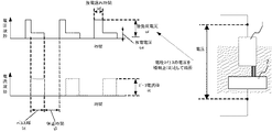
シリコン電極と工作物との間にパルス状の放電を発生させ、工作物表面に耐エロージョン性の機能を有する組織を形成する放電表面処理方法の概略を図1に示す。
図において、1は固体形状の金属シリコン電極(以下、Si電極と記す)、2は処理対象である工作物、3は加工液である油、4は直流電源、5は直流電源4の電圧をSi電極1と工作物2との間に印加或いは停止するためのスイッチング素子、6は電流値を制御するための電流制限抵抗、7はスイッチング素子5のオンオフを制御するための制御回路、8はSi電極1と工作物2の間の電圧を検出し放電が発生したことを検出するための放電検出回路である。FIG. 1 shows an outline of a discharge surface treatment method in which a pulsed discharge is generated between a silicon electrode and a workpiece to form a structure having an erosion resistance function on the workpiece surface.
In the figure, 1 is a solid metal silicon electrode (hereinafter referred to as Si electrode), 2 is a workpiece to be processed, 3 is oil as a machining fluid, 4 is a DC power source, 5 is a voltage of a
次に動作について電圧、電流波形を示した図2を用いて説明する。
制御回路7によりスイッチング素子5をオンすることで、Si電極1と工作物2との間に電圧が印加される。図示しない電極送り機構により、Si電極1と工作物2との間の極間距離は適切な距離(放電が発生する距離)に制御されており、しばらくするとSi電極1と工作物2との間に放電が発生する。予め電流パルスの電流値ieやパルス幅te(放電持続時間)や放電休止時間t0(電圧を印加しない時間)は設定しておき、制御回路7及び電流制限抵抗6により決定される。
放電が発生すると、放電検出回路8により、Si電極1と工作物2との間の電圧の低下とタイミングから放電の発生を検出し、放電発生と検出された時から所定の時間(パルス幅te)後に制御回路7によりスイッチング素子5をオフする。
スイッチング素子5をオフした時から所定の時間(休止時間to)後に再び制御回路7によりスイッチング素子5をオンする。
以上の動作を繰り返し行うことで連続して設定した電流波形の放電を発生させることができる。Next, the operation will be described with reference to FIG. 2 showing voltage and current waveforms.
A voltage is applied between the
When the discharge occurs, the
The
By repeating the above operation, it is possible to generate a discharge having a continuously set current waveform.
尚、図1では、スイッチング素子をトランジスタとして描画しているが電圧の印加を制御できる素子であれば他のものでもよい。また、電流値の制御を抵抗器で行っているように描画しているが、電流値が制御できれば他の方法でもよいことはいうまでない。
また、図2の説明では、電流パルスの波形を矩形波としているが、他の波形でももちろんよい。電流パルスの形により電極をより多く消耗させてSi材料を多く供給させたり、電極の消耗を減らすことで材料を有効に使用するなどのことができるが、本明細書の中では詳細は論じない。In FIG. 1, the switching element is depicted as a transistor, but other elements may be used as long as the application of voltage can be controlled. Further, the current value is drawn as if it was controlled by a resistor, but it goes without saying that other methods may be used as long as the current value can be controlled.
In the description of FIG. 2, the waveform of the current pulse is a rectangular wave, but other waveforms may be used. Depending on the shape of the current pulse, the electrode can be consumed more to supply more Si material, or the electrode can be used effectively by reducing the consumption of the electrode, but the details are not discussed in this specification. .
以上のように連続してSi電極1と工作物2との間に放電を発生させることで、工作物2の表面にSiを多く含んだ層を形成することができる。
しかし安定して本目的にかなう良質のSi含有層を形成するためにはどのようなSiでもよいわけではなく、また、図1の回路にも必要な条件がある。By continuously generating a discharge between the
However, in order to stably form a high-quality Si-containing layer for this purpose, any Si may be used, and the circuit shown in FIG. 1 has necessary conditions.
まず、Si電極及び回路の条件について説明する前に、放電表面処理に関する従来技術と本実施の形態との差異を明確にするために、放電加工による皮膜成形技術について説明する。
シリコンを放電加工の電極として用い、被加工物表面にアモルファス合金層若しくは微細な結晶構造をもつ高耐蝕、高耐熱特性の表面層を形成する手法が特許文献1に開示されている。First, before describing the conditions of the Si electrode and the circuit, a film forming technique by electric discharge machining will be described in order to clarify the difference between the conventional technique related to the discharge surface treatment and the present embodiment.
該公報に開示されたSi電極での放電加工は、電圧印加時間を3μs、休止時間を2μsと固定した周期的に電圧をオンオフする回路方式により、ピーク値Ipが1Aのエネルギを供給し、Φ20mmの面積に対して数時間かけて処理を行なっている。
そのため、電圧を印加している3μsの期間において、放電が電圧パルスのどこで発生するかは全て異なり、実際の放電継続時間である電流が流れる電流パルス幅が逐次変化し、安定した皮膜形成は難しくなる。The electrical discharge machining with the Si electrode disclosed in the publication supplies energy with a peak value Ip of 1 A by a circuit system that periodically turns on and off the voltage with a voltage application time fixed at 3 μs and a pause time of 2 μs. The area is processed for several hours.
Therefore, where the discharge occurs in the voltage pulse is all different in the period of 3μs when the voltage is applied, and the current pulse width through which the current that is the actual discharge duration changes sequentially, making it difficult to form a stable film. Become.
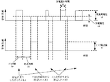
例えば、図3に例示する如く、周期的に電圧をオンオフする回路方式の電源では、電圧波形、電流波形が変化し、パルス毎のエネルギが異なる現象が生じ、電極材料であるSiを工作物に供給する量、および、工作物の表面を溶融させ表面層を作るエネルギがばらばらになるため、安定した処理が困難になる。
なお、図では、放電の電圧は一定、電流も一定としているが、実際には電圧は変動するし、電流も変動する。また、Siのような高抵抗の材料を電極とした場合には、Siでの電圧降下分も含んだ電圧になるため、電圧は高く、また、変動も大きくなる。For example, as illustrated in FIG. 3, in a circuit-type power supply that periodically turns on and off a voltage, a voltage waveform and a current waveform change, and a phenomenon in which energy differs for each pulse occurs. Since the amount to be supplied and the energy for melting the surface of the workpiece to form the surface layer are dispersed, stable processing becomes difficult.
In the figure, the discharge voltage is constant and the current is also constant, but in reality the voltage varies and the current also varies. Further, when a high-resistance material such as Si is used as the electrode, the voltage includes the voltage drop in Si, so that the voltage is high and the fluctuation is large.
次に、特許文献1が上述のように周期的に電圧をオンオフしなければならなかった理由について説明する。
特許文献1では、固有抵抗値0.01Ωcm程度の高抵抗材料であるシリコンを用い、非常に小さな電流パルスの条件を使用している。
そのため、放電のアーク電位を検出することで放電発生を検出する従来の制御方式では、電極が高抵抗材料である場合の放電発生時には、Si電極に電流が流れた場合の電圧降下の電圧が放電のアーク電位に加わった値となり、電圧降下の電圧が高い場合には、放電が発生しているにもかかわらず、回路は放電が発生したと認識できないからである。Next, the reason why
In
Therefore, in the conventional control method that detects the occurrence of discharge by detecting the arc potential of the discharge, when the discharge is generated when the electrode is a high resistance material, the voltage drop voltage when the current flows through the Si electrode is discharged. This is because, when the voltage of the voltage drop is high, the circuit cannot recognize that the discharge has occurred although the discharge has occurred.
また、従来の放電加工によるシリコン皮膜は、処理が大きくばらつき、安定してできないといった問題もあった。
この問題もSiが高抵抗であることに起因している。
例えば、図4に示すように電極の抵抗値Rは抵抗率をρ、面積をS、長さをLとすると、
R=ρ・L/Sとあらわされる。
しかし電極への給電の方法、すなわち、電極の保持方法により、ρが大きい場合にはRの値は大きくばらつくことになってしまう。
従来では、ρ=0.01Ωcmのシリコンを電極として使用しているが、これくらいの高抵抗の材料の場合には、無条件で処理ができるわけではない。例えば、Si電極が長く、一方の端をつかんで給電する場合には、電極が長い場合には、電極の抵抗が高く、短くなるに従い抵抗が低くなる。電極が長く抵抗が高い場合には、上述のように放電を検出できず、異常なパルスが発生する確率も高くなるし、異常が発生しない場合でも抵抗が高いため、放電の電流値が低くなる。In addition, the conventional silicon film formed by electric discharge machining has a problem that the treatment is greatly varied and cannot be stably performed.
This problem is also caused by the high resistance of Si.
For example, as shown in FIG. 4, when the resistance value R of the electrode is ρ as the resistivity, S as the area, and L as the length,
R = ρ · L / S.
However, depending on the method of supplying power to the electrode, that is, the method of holding the electrode, the value of R will vary greatly if ρ is large.
Conventionally, silicon with ρ = 0.01 Ωcm is used as an electrode. However, in the case of such a high resistance material, processing cannot be performed unconditionally. For example, when the Si electrode is long and the power is fed by holding one end, when the electrode is long, the resistance of the electrode is high, and the resistance decreases as the length becomes short. If the electrode is long and has high resistance, the discharge cannot be detected as described above, and the probability of occurrence of an abnormal pulse increases, and even if no abnormality occurs, the resistance is high, so the discharge current value is low. .
発明者らの研究では、ρ=0.01Ωcm程度の抵抗値のシリコンを電極として使用する場合、電極長さが数10mm程度以上になると放電が発生した場合の電流による電極での電圧降下が大きくなり異常な放電が発生し正常な表面層の形成が困難となる場合があった。
また、このような異常な放電が起きる条件は、ほぼ、給電位置と放電の位置、すなわち、電極の長さによって決まり、電極の面積(太さ)にはあまり関係ないことがわかった。
これは、電流が電極内を流れる際に電極の断面全体を均一に流れるのではなく、ある細い経路を流れるからであると推測できる。したがって、0.01Ωcm以上の抵抗率のシリコンを電極として用いても放電が発生する位置と給電点を近くすれば安定した放電を発生させることは可能になる。例えば、1mm程度の板状のシリコンを金属に接合して給電すれば、抵抗値が0.05Ωcm程度でも安定した放電は可能であった。しかし、0.01Ωcmの電極でもある程度の長さ以上、例えば100mm程度以上の長さになると、異常な放電が発生する場合があり、安定した処理は困難であった。According to the inventors' research, when silicon having a resistance value of about ρ = 0.01 Ωcm is used as an electrode, if the electrode length exceeds about several tens of millimeters, the voltage drop at the electrode due to the current when a discharge occurs increases. In some cases, abnormal discharge occurs, making it difficult to form a normal surface layer.
Further, it has been found that the conditions under which such abnormal discharge occurs are almost determined by the feeding position and the discharge position, that is, the length of the electrode, and are not so much related to the area (thickness) of the electrode.
This can be presumed to be because when the current flows through the electrode, it does not flow uniformly across the entire cross section of the electrode, but flows through a narrow path. Therefore, even when silicon having a resistivity of 0.01 Ωcm or more is used as an electrode, it is possible to generate a stable discharge if the position where the discharge is generated is close to the feeding point. For example, if a plate-shaped silicon of about 1 mm is bonded to a metal and supplied with power, stable discharge was possible even with a resistance of about 0.05 Ωcm. However, even with an electrode of 0.01 Ωcm, if the length exceeds a certain length, for example, about 100 mm or more, abnormal discharge may occur, and stable treatment is difficult.
以上の議論のように発明者らの実験から以下のことが明らかとなった。
・シリコンを電極として油中でのパルス放電を利用して工作物の表面にSiを含む表面層を、工業的に使用に耐えるように10μm程度の厚みで高速に形成するためには、従来開示されているような方法では不可能であり、図1、図2に示したような放電のパルス幅(放電電流パルス)を制御(ほぼ同じパルス幅にそろえる)する方式の回路を使用し、適切なエネルギーのパルスを使用しなければならない。As described above, the following was clarified from experiments by the inventors.
In order to form a surface layer containing Si on the surface of a workpiece with silicon as an electrode at a high speed of about 10 μm so that it can be used industrially, it has been disclosed in the past. It is not possible with the method as described above, and the circuit of the system for controlling the discharge pulse width (discharge current pulse) as shown in FIGS. Must use a pulse of correct energy.
・シリコンを電極として工作物表面に10μm程度の表面層を形成するためには、抵抗値(比抵抗)は低い方がよい。工業的な実用を考慮し、電極の長さが100mm程度以上でも使用する場合を考えるとρが0.005Ωcm程度以下であることが望ましい。Siの抵抗値を下げるには、他の元素をドーピングするなど、いわゆる不純物の濃度を増せばよい。 In order to form a surface layer of about 10 μm on the workpiece surface using silicon as an electrode, the resistance value (specific resistance) should be low. In consideration of industrial practical use, it is desirable that ρ is about 0.005 Ωcm or less, considering the case where the electrode is used even if the length of the electrode is about 100 mm or more. In order to reduce the resistance value of Si, the concentration of so-called impurities may be increased, such as doping with other elements.
・ρが0.005Ωcm以上であっても、給電点と放電位置が近い場合には、安定した処理が可能である。その際の指標は、ρが0.005Ωcm以下の場合も含めて以下のようにすればよい。以下のような方法を取ればρが0.02Ωcm程度でも処理ができる場合もある。
すなわち、極間に印加する電圧が低下したことにより放電が発生したと認識し、その放電が発生したと認識した時点から所定の時間(パルス幅te)経過した後に電圧の印加を停止(すなわち放電を停止)させる電源により、Siを電極として工作物表面にSiを含む表面層を形成する際に、放電が発生した際の抵抗体であるSi電極での電圧降下を含んだ極間電圧が、放電検出レベルよりも低くなる状態で処理を行えばよい。Even if ρ is 0.005 Ωcm or more, stable treatment is possible if the feeding point and the discharge position are close. The index at that time may be as follows including the case where ρ is 0.005 Ωcm or less. If the following method is used, processing may be possible even if ρ is about 0.02 Ωcm.
That is, it is recognized that a discharge has occurred due to a decrease in the voltage applied between the electrodes, and the application of the voltage is stopped after a predetermined time (pulse width te) has elapsed from the time when the discharge has been recognized (that is, the discharge) When a surface layer containing Si is formed on the workpiece surface using Si as an electrode, the interelectrode voltage including a voltage drop at the Si electrode, which is a resistor when a discharge occurs, What is necessary is just to process in the state which becomes lower than a discharge detection level.
一般的にアークの電位は25V〜30V程度であるが、放電検出レベルの電圧は、電源電圧よりも低く、アークの電位よりも高く設定すればよい。しかし、放電検出レベルを低く設定すれば、Siの抵抗値は低くしなければ放電が発生しても放電が発生したと認識できず、図5に示したような異常な長いパルスが生じてしまう危険が増える。
放電検出レベルを高く設定すれば、Siの抵抗がやや高くても放電が発生した場合には放電検出レベルを下回りやすくなる。すなわち、Siの抵抗値が低い場合には、電極が長くともよく、Siの抵抗値が高い場合には、Siの長さを短くして、放電が発生した場合の極間電圧が放電検出レベルよりも低くなるようにすればよい。放電検出レベルは、電源電圧よりも低く、アークの電位よりも高く設定すればよいが、以上の説明から、電源電圧よりもわずかに低いレベルに設定するのがよい。
発明者らの実験では、主電源の電圧よりも10V〜30V程度低い値に設定することが実用上もっとも汎用性があることがわかった。より厳密には、10V〜20V程度電源電圧よりも低い値とするのが使用できるSiにも幅ができて都合がよかった。ここでいっている主電源とは、放電を発生・継続させる電流を流すための電源のことであり、放電を発生させるために高圧の電圧を引加するための高圧重畳回路の電源ではない。(詳細はここでは論じない)In general, the arc potential is about 25 V to 30 V, but the discharge detection level voltage may be set lower than the power supply voltage and higher than the arc potential. However, if the discharge detection level is set to a low value, it cannot be recognized that a discharge has occurred unless the resistance value of Si is low, and an abnormally long pulse as shown in FIG. 5 is generated. The danger increases.
If the discharge detection level is set high, even if the resistance of Si is slightly high, it becomes easy to fall below the discharge detection level when a discharge occurs. That is, when the resistance value of Si is low, the electrode may be long. When the resistance value of Si is high, the length of Si is shortened, and the voltage between the electrodes when discharge occurs is the discharge detection level. It is sufficient to make it lower. The discharge detection level may be set lower than the power supply voltage and higher than the arc potential, but from the above description, it is preferable to set the discharge detection level slightly lower than the power supply voltage.
In the experiments by the inventors, it has been found that setting the value about 10V to 30V lower than the voltage of the main power supply has the most versatility in practice. More strictly, Si that can be used having a value lower than the power supply voltage by about 10 V to 20 V is convenient because of the wide width. The main power source mentioned here is a power source for supplying a current for generating / continuing a discharge, and is not a power source for a high voltage superposition circuit for applying a high voltage to generate a discharge. (Details are not discussed here)
以上のような条件を満たすことで、高抵抗材料であるSiを電極として用いて、自在な放電パルスを安定して発生させることができ、Siを含む表面層を工作物に形成することができる。 By satisfying the above conditions, it is possible to stably generate a free discharge pulse using Si, which is a high resistance material, as an electrode, and to form a surface layer containing Si on a workpiece. .
さて、以上のようなSiを含む表面層ができるようになり、その性質を調べたところ以下のようなことがわかってきた。
図6はSiを含む表面層の分析結果である。
Siの層は工作物の表面にSiのみの単層が形成されているわけではなく、工作物の表面に工作物の材料とSiが混ざったSiと工作物の混合層ができていることがわかる。
図6において、上段左写真がSi表面層断面のSEM写真、上段中がSiの面分析結果、上段右はCrの面分析結果、下段左はFeの面分析結果、下段右(中)はNiの面分析結果である。
以上よりわかるようにSi表面層はSiが母材の上にのっているのではなく、母材の表面部分にSi濃度が高くなった部分として形成されていることがわかる。
この結果からある程度の厚みがある表面層になっているが、Siが母材と一体化しており、母材にSiが高濃度で浸透したような状態の表面層になっていることがわかる。この表面層はSiの含有量を増した鉄基金属組織であり、皮膜という表現は適切ではないため、以下簡単のため、Si表面層と呼ぶことにする。
このような状態であるので、表面層は他の表面処理方法とは異なり被膜が剥離することはない。この表面層について調べた結果、高い耐食性があることが確認できた。また、ある条件を満たす場合には極めて高い耐エロージョン性があることがわかった。エロージョンとは、部材に水などがあたり浸食する現象であり、水や蒸気の通る配管部品、あるいは、蒸気タービンの動翼などの故障の原因となる現象である。Now, a surface layer containing Si as described above can be formed, and when the properties thereof are examined, the following has been found.
FIG. 6 shows the analysis result of the surface layer containing Si.
The Si layer is not a single layer of Si only on the surface of the workpiece, but a mixed layer of Si and the workpiece, in which the workpiece material and Si are mixed, is formed on the surface of the workpiece. Recognize.
In FIG. 6, the upper left photograph is an SEM photograph of the Si surface layer cross section, the upper middle is the Si surface analysis result, the upper right is the Cr surface analysis result, the lower left is the Fe surface analysis result, and the lower right (middle) is Ni. It is a surface analysis result.
As can be seen from the above, it can be seen that the Si surface layer is not formed on the base material, but is formed as a portion having a high Si concentration on the surface portion of the base material.
From this result, it can be seen that the surface layer has a certain thickness, but Si is integrated with the base material, and the surface layer is in a state where Si penetrates the base material at a high concentration. Since this surface layer is an iron-based metallographic structure with an increased Si content and the expression “film” is not appropriate, it will be referred to as an Si surface layer for the sake of simplicity.
Since it is in such a state, the surface layer does not peel off the coating unlike the other surface treatment methods. As a result of investigating this surface layer, it was confirmed that it had high corrosion resistance. Further, it was found that when a certain condition is satisfied, there is extremely high erosion resistance. Erosion is a phenomenon in which water or the like hits and erodes a member, and is a phenomenon that causes failure of piping parts through which water or steam passes, or a moving blade of a steam turbine.
ここで、以後本明細書中で論じる耐食性、耐エロージョン性を評価する方法について説明しておく。 Here, a method for evaluating corrosion resistance and erosion resistance, which will be discussed later in this specification, will be described.
・耐食性
耐食性については、皮膜を形成した試験片を王水に浸して腐食の様子を観察する方法を取った。試験の様子の例を図7に示す。試験片の一部にSi表面層を形成し、王水に浸漬して表面層部分の腐食の様子、表面層以外の部分の腐食の様子を観察した。図7では、試験片の中央部分に(10mm×10mmの)Si表面層が形成されている。本明細書中の王水による腐食試験では、王水に60分浸漬して表面の観察を行った。また、試験片に塩水を噴霧して錆の発生を観察する塩水噴霧試験、塩水に浸漬して錆の発生を見る塩水浸漬試験なども行い、耐食性を判断したが、詳細は本明細書中では省略する。-Corrosion resistance As for corrosion resistance, a method was adopted in which a test piece having a film formed was immersed in aqua regia to observe the state of corrosion. An example of the state of the test is shown in FIG. A Si surface layer was formed on a part of the test piece and immersed in aqua regia to observe corrosion of the surface layer portion and corrosion of portions other than the surface layer. In FIG. 7, a Si surface layer (10 mm × 10 mm) is formed at the center of the test piece. In the corrosion test with aqua regia in this specification, the surface was observed by immersing in aqua regia for 60 minutes. In addition, the salt spray test to observe the occurrence of rust by spraying salt water on the test piece, the salt water immersion test to observe the occurrence of rust by immersing in salt water, etc. were performed, and the corrosion resistance was judged. Omitted.
・耐エロージョン性評価試験
耐エロージョン性能の評価としては、図8に示すように、試験片にウォータージェットを当てて浸食の様子を比較した試験を行なった。ここでまず、所定の条件を満たすSi表面層の高い耐エロージョン性を示す実験結果について説明する。所定の条件については後述する。
本実施の形態の耐エロージョン性能について以下に試験結果を説明する。耐エロージョンの評価として試験片にウォータージェットを当てて浸食の様子を比較した。
ウォータージェットは200MPaの圧力で当てた。試験片としては、1)ステンレス基材、2)ステライト(一般的に、耐エロージョン用途に使用される材料)、3)放電によるTiC皮膜をステンレス基材表面に形成したもの、4)本発明によるSiの多い表面層をステンレスに形成したもの、の4種類を使用した。
3)の皮膜は、国際公開番号WO01/005545に開示されている方法により形成したTiC皮膜であり、高い硬さを持っている被膜である。
それぞれの試験片に10秒間ウォータージェットを当て、試験片の浸食をレーザー顕微鏡により測定した。-Erosion resistance evaluation test As shown in Fig. 8, an evaluation of the erosion resistance performance was performed by applying a water jet to the test piece and comparing the state of erosion. First, experimental results showing the high erosion resistance of the Si surface layer satisfying the predetermined conditions will be described. The predetermined condition will be described later.
The test results of the erosion resistance performance of this embodiment will be described below. As an evaluation of erosion resistance, the state of erosion was compared by applying a water jet to the test piece.
The water jet was applied at a pressure of 200 MPa. Test specimens include 1) stainless steel substrate, 2) stellite (a material generally used for erosion-resistant applications), 3) a TiC film formed by discharge on a stainless steel substrate surface, and 4) according to the present invention. Four types were used: a Si-rich surface layer formed on stainless steel.
The film 3) is a TiC film formed by the method disclosed in International Publication No. WO01 / 005545, and has a high hardness.
A water jet was applied to each test piece for 10 seconds, and the erosion of the test piece was measured with a laser microscope.
図9は1)の結果、図10は2)の結果、図11は3)の結果、図12は4)すなわち本実施の形態による表面層の場合の結果である。
図9に示される如く、ステンレス基材では10秒間ウォータージェットを当てた場合に約100μmの深さまで浸食されている。
それに対し、図10に示される如く、ステライト材では、浸食の様子が異なるものの、深さは60〜70μm程度であり、ステライト材での耐エロージョン性がある程度確認できた。
図11は、硬さの非常に高いTiC被膜の結果であるが、約100μmの深さまで浸食されており、耐エロージョンが表面の硬さだけによるのではないことがわかる結果となった。9 shows the result of 1), FIG. 10 shows the result of 2), FIG. 11 shows the result of 3), and FIG. 12 shows the result of 4), that is, the surface layer according to the present embodiment.
As shown in FIG. 9, the stainless steel substrate is eroded to a depth of about 100 μm when a water jet is applied for 10 seconds.
On the other hand, as shown in FIG. 10, the stellite material has a different erosion state, but the depth is about 60 to 70 μm, and the erosion resistance of the stellite material was confirmed to some extent.
FIG. 11 shows the result of the TiC film having a very high hardness, but it was found that the erosion resistance was not solely due to the hardness of the surface because it was eroded to a depth of about 100 μm.
一方、図12は本実施の形態によるSiの表面層の場合の結果であるが、ほとんど浸食されていないことがわかる。
この表面層の硬さは約800HV程度(表面層の厚みが薄いため荷重10gとしてマイクロビッカース硬さ計で測定した。硬さの範囲は、おおよそ600〜1100HVの範囲であった)であり、1)に示されるステンレス基材(350HV程度)や、2)に示されるステライト材(420HV程度)に比べると高いものの、3)に示されるTiC皮膜(約1500HV)に比べると硬さは低い。
すなわち、耐エロージョン性は硬さだけでなく、他の性質も合わせた複合的な効果であることがわかる。On the other hand, FIG. 12 shows the result in the case of the surface layer of Si according to the present embodiment.
The hardness of this surface layer is about 800 HV (the thickness of the surface layer was so thin that it was measured with a micro Vickers hardness tester with a load of 10 g. The hardness range was approximately 600 to 1100 HV). The hardness is lower than that of the TiC film (about 1500 HV) shown in 3), although it is higher than the stainless steel substrate (about 350 HV) shown in 2) and the stellite material (about 420 HV) shown in 2).
That is, it can be seen that the erosion resistance is a combined effect that combines not only the hardness but also other properties.
図11では、硬い被膜であるにもかかわらず、えぐり取られたようにみえることから、表面だけ硬い場合でも表面に靭性がない薄い被膜の場合にはウォータージェットの衝撃で破壊されてしまうと推察される。
それに対して本実施の形態における4)の被膜は後述する表面層の結晶構造に加え、靭性があり、変形にも耐えられる表面になっており、その点が高い耐エロージョン性を示す原因であると推察している。In FIG. 11, although it is a hard coating, it seems that it has been scooped out, so even if only the surface is hard, it is assumed that the thin coating with no toughness on the surface will be destroyed by the impact of the water jet. Is done.
On the other hand, the film of 4) in the present embodiment has a tough surface that can withstand deformation, in addition to the crystal structure of the surface layer described later, and this is the cause of high erosion resistance. I guess.
4)の表面層は厚さ5μm程度の厚さで試験しているが、被膜が薄い場合にはやはり強度が十分ではなく浸食がおきやすくなることを別途確認している。
先行技術である特許文献1では、Siの被膜について研究され、高い耐食性は明らかとされたにもかかわらず耐エロージョン性については発見できなかったのは表面層を厚くできなかったことが大きな原因の1つであると推察できる。
耐エロージョンの場合には、水などのエロージョンの原因となる物質の衝突する速度にもよるが、5μm以上の表面層のあることが望ましい。もちろん衝突する物質により望ましい厚みは変わり、例えば速度の速い場合や滴の大きい場合には厚めの方が望ましい。The surface layer of 4) has been tested with a thickness of about 5 μm, but it has been confirmed separately that when the coating is thin, the strength is not sufficient and erosion easily occurs.
In
In the case of erosion resistance, it is desirable to have a surface layer of 5 μm or more, although it depends on the collision speed of substances that cause erosion such as water. Of course, the desired thickness varies depending on the colliding substance. For example, when the velocity is high or the droplet size is large, a thicker thickness is desirable.
4)に示されるSiの表面層に対する試験ではほとんど浸食が確認できなかったので、さらにSiの表面層に対する試験を延長して60秒間連続してウォータージェットを当てた結果を図13に示す。
ウォータージェットが当たった場所が少し磨かれた状態になり判別はできるが、ほとんど磨耗はしていないことがわかる。
以上より、本実施の形態の表面層の高い耐エロージョン性が確認できた。Since almost no erosion could be confirmed in the test for the Si surface layer shown in 4), FIG. 13 shows the result of extending the test for the Si surface layer and applying a water jet continuously for 60 seconds.
The place where the water jet hit is a little polished and can be distinguished, but it can be seen that there is almost no wear.
From the above, high erosion resistance of the surface layer of the present embodiment was confirmed.
以上のような、耐エロージョン性、耐食性を得るためには2つの重要な要素があることがわかった。1つは成膜条件であり、もう1つは皮膜を形成する時間、より正確に言うと処理の進行具合、である。以下にそれぞれについてより詳細に説明する。 As described above, it has been found that there are two important factors for obtaining erosion resistance and corrosion resistance. One is the film forming conditions, and the other is the time for forming the film, more precisely, the progress of the process. Each will be described in more detail below.
まず1つ目の要素である成膜条件について論じる。
成膜条件の影響についてウォータージェットによる耐エロージョン性の評価結果から説明する。
図14に示した各条件での被膜にウォータージェットを当てて浸食の様子を調べた。
図14には、各処理条件に対し、その条件の放電パルスのエネルギーに相当する値である放電パルスの電流値の時間積分の値(A・μs)(矩形波であれば、電流値ie×パルス幅te)、その処理条件でのSi表面層の厚み、Si表面層のクラックの有無を示している。
処理条件は、横軸に電流値ie、縦軸にパルス幅teとして、その値の矩形波の電流パルスを使用した。この試験に使用した基材はSUS630である。
Siはρ=0.01Ωcmのものを使用し、放電パルスが正常に発生する範囲のサイズの電極を作成し、試験を行なった。図からわかるように、成膜条件、すなわち、放電パルスのエネルギーは、皮膜の厚さ(膜厚)と密接に関係があり、ほぼ、放電パルスのエネルギーと膜厚とは比例しているということができる。First, the film forming conditions as the first element will be discussed.
The influence of film forming conditions will be described from the evaluation results of erosion resistance by a water jet.
The state of erosion was examined by applying a water jet to the coating film under each condition shown in FIG.
FIG. 14 shows, for each processing condition, the value (A · μs) of the time integral of the current value of the discharge pulse, which is a value corresponding to the energy of the discharge pulse of that condition (current value ie × The pulse width te), the thickness of the Si surface layer under the processing conditions, and the presence or absence of cracks in the Si surface layer are shown.
The processing conditions were as follows: current value ie on the horizontal axis and pulse width te on the vertical axis, and rectangular wave current pulses of that value. The base material used for this test is SUS630.
Si having ρ = 0.01 Ωcm was used, and an electrode having a size within a range in which a discharge pulse was normally generated was prepared and tested. As can be seen from the figure, the deposition conditions, that is, the energy of the discharge pulse, is closely related to the thickness (film thickness) of the film, and the energy of the discharge pulse and the film thickness are almost proportional. Can do.
図より、Si表面層の形成条件の1つとして、クラックの有無について見ることができる。クラックの有無は放電パルスのエネルギーと相関が強く、放電パルスのエネルギー相当量である放電電流の時間積分値が80A・μs以下の範囲にあることがクラックのないSi表面層を形成するための条件であることがわかる。 From the figure, the presence or absence of cracks can be seen as one of the conditions for forming the Si surface layer. The presence or absence of cracks has a strong correlation with the energy of the discharge pulse, and the time integral value of the discharge current, which is equivalent to the energy of the discharge pulse, is in the range of 80 A · μs or less. It can be seen that it is.
もちろん加工条件によりクラックが入るか入らないかは、基材にも多少は影響を受ける。
例えばステンレス鋼と呼ばれる材料の中でも、SUS304のような固溶体である材料は比較的クラックが入りにくく、SUS630のような析出硬化型の材料では若干クラックが入りやすい傾向がある。蒸気タービンには一般的にSUS630等の析出硬化型のステンレス鋼が用いられるので、クラックの入らない望ましい範囲はSUS304のようなオーステナイト系のステンレス鋼よりは若干狭くなる。Of course, whether or not cracks occur depending on the processing conditions is also somewhat affected by the substrate.
For example, among materials called stainless steel, a solid solution material such as SUS304 is relatively hard to crack, and a precipitation hardening type material such as SUS630 tends to crack a little. Since a precipitation hardening type stainless steel such as SUS630 is generally used for the steam turbine, a desirable range in which cracks do not occur is slightly narrower than that of an austenitic stainless steel such as SUS304.
Si表面層の厚みが放電パルスのエネルギー相当量である放電電流の時間積分値と相関があり、放電電流の時間積分値が小さいと厚みが小さくなり、放電電流の時間積分値が大きいと厚みも大きくなる旨前述したが、ここで言うところの厚みはすなわち放電のエネルギーで溶融し、電極成分であるSiが進入した範囲のことを言っている。
熱の影響の範囲は放電パルスのエネルギーの大きさ相当量である放電電流の時間積分値の大きさで決まるが、進入するSiの量は放電の発生回数も影響する。放電が少ない場合には当然のことながらSiが十分に進入できないので、Si表面層のSiの量は少なくなる。逆に十分以上に放電が発生してもSi表面層のSi量はある値で飽和する。この点については、後に2つめの要素である皮膜の形成時間について論じるところで詳細説明する。The thickness of the Si surface layer correlates with the time integral value of the discharge current, which is equivalent to the energy of the discharge pulse, and the thickness decreases when the time integral value of the discharge current is small, and the thickness also increases when the time integral value of the discharge current is large. As described above, the thickness becomes larger, that is, the thickness that is melted by the energy of discharge, and refers to the range where Si as an electrode component enters.
The range of the influence of heat is determined by the magnitude of the time integration value of the discharge current, which is an amount corresponding to the magnitude of the energy of the discharge pulse, but the amount of Si that enters also affects the number of occurrences of discharge. When the discharge is small, it is natural that Si cannot sufficiently enter, so the amount of Si in the Si surface layer is small. On the other hand, even if discharge occurs more than enough, the Si amount in the Si surface layer is saturated at a certain value. This point will be described in detail later when discussing the film formation time, which is the second factor.
説明が後になったが、Si表面層の性能について以下に論じる。
なお、エロージョンには大きく2つのモードがあり、1つは水の衝撃で大きく抉り取られるモード、もう1つは水が強く当たり表面を流れる際に表面を引っかき削りとるモードである。
図15は厚さ3μmのSi表面層にウォータージェットを200MPaで60秒当てたときにSi表面層が破壊された結果である。細かく剥ぎ取られたような痕は見えないものの、大きく抉り取られるように破壊されていることがわかる。これは、水の衝突により擦り取られた傷ではなく、ウォータージェットで大量の水を当てているための衝撃にSi表面層が耐えられずに破壊された結果であると考えられる。すなわち、Si表面層が4μm以下と薄い場合には、水が強く当たり表面を流れる際に表面を引っかき削りとるモードに対してはある程度効果があるが、水の衝撃で大きく抉り取られるモードに対しては、効果が少ないということを示している。
また、図16は耐エロージョン性が高いとされる材料であるステライトNo6であり、90MPaのウォータージェットを60秒当てた場合の結果である。図では、水が強く当たり表面を流れる際に表面を引っかき削りとるモードを示している。Although explained later, the performance of the Si surface layer is discussed below.
There are two major modes of erosion. One is a mode in which the surface is greatly scraped off by the impact of water, and the other is a mode in which the surface is scraped off when the water is strongly hit and flows through the surface.
FIG. 15 shows the result of destruction of the Si surface layer when a water jet was applied to the Si surface layer having a thickness of 3 μm at 200 MPa for 60 seconds. It can be seen that although the traces that were finely peeled off are not visible, they are destroyed so as to be largely scraped off. This is considered to be a result of the Si surface layer being destroyed without being able to withstand the impact caused by the application of a large amount of water with a water jet, not the scratches scraped off by the collision of water. That is, when the Si surface layer is as thin as 4 μm or less, it is effective to some extent for the mode in which the surface is scratched when the water hits the surface strongly. Shows that the effect is small.
FIG. 16 shows Stellite No6, which is a material with high erosion resistance, and shows the result when a 90 MPa water jet is applied for 60 seconds. The figure shows a mode in which the surface is scraped off when the water is strongly hit and flows through the surface.
次に、Si表面層の厚さと耐エロージョン性との関係を図17に示す。
図に示されるように、Si表面層の厚さが4μm以下では蒸気タービンで水滴がタービン翼に衝突する速度相当である音速程度の速度でウォータージェットを当てた場合には、Si表面層が薄いと被膜が耐えられず、表面が破壊される現象が高い確率で発生することがわかった。
Si表面層の厚みが薄いと衝撃に弱く、厚いと衝撃に強い理由は以下のように推察している。すなわち、Si表面層が薄い場合には、衝撃を受けていると歪が基材に徐々に蓄積され最後に母材の粒界から破壊が発生するが、Si表面層が厚い場合には、歪が母材に達しにくく基材が守られる一方で、Si表面層は非晶質な組織であるため粒界がなく粒界での破壊に至らないということである。
この観点で、Si表面層を厚くするためには、放電パルスのエネルギーを大きくする必要があり、5μm以上にするためには、放電パルスのエネルギーは30A・μs以上である必要があることがわかった。Next, the relationship between the thickness of the Si surface layer and the erosion resistance is shown in FIG.
As shown in the figure, when the thickness of the Si surface layer is 4 μm or less, the Si surface layer is thin when the water jet is applied at a speed of about the speed of sound that is equivalent to the speed at which water droplets collide with the turbine blades in the steam turbine. It was found that the phenomenon that the film could not be tolerated and the surface was destroyed occurred with high probability.
The reason why the Si surface layer is thin is weak against impact, and when the Si surface layer is thick, the reason for strong shock is presumed as follows. That is, when the Si surface layer is thin, strain is gradually accumulated on the base material when impact is applied, and finally the fracture occurs from the grain boundary of the base material. However, when the Si surface layer is thick, the strain is However, the Si surface layer is an amorphous structure, so that there is no grain boundary and no breakage occurs at the grain boundary.
From this point of view, it is necessary to increase the energy of the discharge pulse in order to increase the thickness of the Si surface layer, and it is necessary to increase the energy of the discharge pulse to 30 A · μs or more in order to increase the thickness to 5 μm or more. It was.
以上のようにSi表面層の膜厚を厚くすることで耐エロージョン性を上げることができるが、一方で、膜厚を厚くすることに伴う問題もあり、そのことが原因で耐エロージョン性を悪化させることがある。前述のように、Si表面層を厚くするためには、放電パルスのエネルギーを大きくする必要があるが、放電のエネルギーを大きくするに従い、熱の影響も大きくなり、表面にクラックが発生するようになる。クラックは、放電パルスのエネルギーが大きくなるほど入りやすくなり、前述のように、80A・μs以上のパルスで処理した場合には表面にクラックが入るようになる。
表面にクラックが入ると耐エロージョン性が著しく低下することがわかった。図18は80A・μs以上の放電パルス条件で処理したSi表面層に、ウォータージェットを当てることでクラックが進展した様子を示している。さらに継続するとある範囲で大きく被膜が破壊される。80A・μsのエネルギーのパルス条件で処理した場合に膜厚は10μm程度になり、これが事実上の耐エロージョン用途のSi表面層の上限値になることがわかった。
クラックの観点で、Si表面層の膜厚と耐エロージョン性との関係を図示すると、図19のようになる。図17と図19をあわせると、Si表面層の膜厚と耐エロージョン性との関係は図20のようになることがわかった。As described above, the erosion resistance can be increased by increasing the film thickness of the Si surface layer, but there is also a problem associated with increasing the film thickness, which deteriorates the erosion resistance. There are things to do. As described above, in order to increase the thickness of the Si surface layer, it is necessary to increase the energy of the discharge pulse. However, as the discharge energy is increased, the influence of heat increases and cracks are generated on the surface. Become. Cracks are more likely to enter as the energy of the discharge pulse increases, and as described above, cracks appear on the surface when treated with a pulse of 80 A · μs or more.
It was found that the erosion resistance is remarkably lowered when cracks are formed on the surface. FIG. 18 shows a state in which cracks have progressed by applying a water jet to a Si surface layer treated under a discharge pulse condition of 80 A · μs or more. If it continues further, a film will be destroyed greatly within a certain range. It was found that when the film was processed under a pulse condition of energy of 80 A · μs, the film thickness was about 10 μm, and this was the practical upper limit value of the Si surface layer for erosion resistance.
From the viewpoint of cracks, the relationship between the film thickness of the Si surface layer and the erosion resistance is illustrated in FIG. When FIG. 17 and FIG. 19 are combined, it has been found that the relationship between the film thickness of the Si surface layer and the erosion resistance is as shown in FIG.
以上をまとめると次のようになる。耐エロージョン性を有するSi表面層を形成するためには、Si表面層を5μm以上にすることが必要であり、そのためには放電パルスのエネルギーは30A・μs以上である必要がある。
一方で、表面のクラックを防止するためには、放電パルスのエネルギーは80A・μs以下であることが必要であり、そのためSi表面層は10μm以下となる。
すなわち、耐エロージョン性を有するSi表面層を形成するための条件は被膜厚さが5μm〜10μmの厚みの被膜であり、そのための放電パルスのエネルギーが30A・μs〜80A・μsである。そのときの被膜硬さは、600HV〜1100HVの範囲である。The above is summarized as follows. In order to form a Si surface layer having erosion resistance, the Si surface layer needs to be 5 μm or more, and for this purpose, the energy of the discharge pulse needs to be 30 A · μs or more.
On the other hand, in order to prevent cracks on the surface, the energy of the discharge pulse needs to be 80 A · μs or less, and therefore the Si surface layer is 10 μm or less.
That is, the condition for forming the erosion-resistant Si surface layer is a film having a film thickness of 5 μm to 10 μm, and the energy of the discharge pulse for that is 30 A · μs to 80 A · μs. The film hardness at that time is in the range of 600 HV to 1100 HV.
以上、エロージョンの観点から成膜条件について説明したが、耐食性についても、ほぼ同じ傾向が見られることがわかってきた。鋼材にSi表面層を形成すると、高い耐食性が得られることが報告されている。しかし、これは成膜条件、素材の影響を大きく受けることがわかってきた。耐食性についても、放電パルスのエネルギーは80A・μs以下でクラックのない表面にすることが極めて重要である。クラックが発生した面では、クラックから腐食が進行し、材料としての耐食性は期待できない。 As described above, the film forming conditions have been described from the viewpoint of erosion, but it has been found that the same tendency can be seen in the corrosion resistance. It has been reported that high corrosion resistance can be obtained when a Si surface layer is formed on a steel material. However, it has been found that this is greatly influenced by film forming conditions and materials. In terms of corrosion resistance, it is extremely important that the energy of the discharge pulse is 80 A · μs or less and that the surface is free from cracks. On the surface where the crack occurs, corrosion proceeds from the crack, and corrosion resistance as a material cannot be expected.
また、逆に放電パルスのエネルギーが小さく、皮膜が薄い場合には、実用上耐食性が十分えられない場合が多いこともわかった。皮膜厚さに必要な条件を考える場合には、どのような素材に成膜するかについても考慮する必要がある。上記試験は、SUS630を用いて行なったが、本発明の重要な適用対象として、金型分野がある。金型分野に使用される主要な材料である冷間ダイス鋼SKD11、部品などに使用される材料である機械構造用炭素鋼S−C材等でも同様の耐食試験を行った。
SUS630やSUS302は析出物があまりない、あるいは、あっても比較的小さい材料である。一方で、SKD11やS50C等のように析出物が大きい材料については、表面層が薄い場合には、表面層に欠陥が発生する。析出物が表面層の中にあるために、表面層の耐食性を損ねたり、エロージョンの起点になる。また、放電が発生するときに、析出物は基材と放電の発生のしやすさ、あるいは、放電が発生したときの材料の除去され具合が異なるため、表面層に欠陥をつくる原因になる。On the other hand, it was also found that when the energy of the discharge pulse is small and the film is thin, the corrosion resistance is often insufficient in practice. When considering the conditions necessary for the film thickness, it is necessary to consider what kind of material the film is to be formed on. Although the above test was performed using SUS630, there is a mold field as an important application object of the present invention. The same corrosion resistance test was also performed on cold die steel SKD11, which is the main material used in the mold field, and carbon steel S—C material for mechanical structures, which is a material used for parts and the like.
SUS630 and SUS302 are materials with little or no precipitate. On the other hand, for materials with large precipitates such as SKD11 and S50C, defects occur in the surface layer when the surface layer is thin. Since precipitates are present in the surface layer, the corrosion resistance of the surface layer is impaired and erosion starts. In addition, when discharge occurs, the precipitates cause defects in the surface layer because the base material and the ease of occurrence of the discharge or the removal of the material when the discharge occurs are different.
図21は金型分野等で頻繁に使用される冷間ダイス鋼SKD11の表面に先行技術の条件に近い条件で約3μm程度のSi表面層を形成した様子を示している。また、図22は冷間ダイス鋼SKD11の表面に先行技術の条件に近い条件で約3μm程度のSi表面層を形成した後、王水で腐食した状態の写真を示している。一般的に頻繁に使用される材料において、約3μmのSi表面層では、十分な耐食性が得られないことがわかった。このときの処理時間は後述する最適な処理時間で行っている。なお、3μm程度の表面層を形成したときには、図3に示したような先行技術の方式の電源回路方式ではなく、本発明の電源方式で先行技術の条件相当の条件を使用していることを申し添えておく。 FIG. 21 shows a state in which a Si surface layer of about 3 μm is formed on the surface of cold die steel SKD11 frequently used in the mold field or the like under conditions close to those of the prior art. FIG. 22 shows a photograph of a state in which a Si surface layer of about 3 μm is formed on the surface of the cold die steel SKD11 under conditions close to those of the prior art and then corroded with aqua regia. It has been found that, in a material that is generally frequently used, sufficient corrosion resistance cannot be obtained with a Si surface layer of about 3 μm. The processing time at this time is an optimum processing time described later. When a surface layer of about 3 μm is formed, it is necessary to use conditions equivalent to the conditions of the prior art in the power supply system of the present invention instead of the power supply circuit system of the prior art system as shown in FIG. I will tell you.
一方で、図23は、同じく各種材料に10μm程度のSi表面層を形成した場合の表面写真である。5μm以上10μm程度の表面層形成条件になると、2μmの表面層の時に問題になった表面の欠陥はなく、均一に表面層が形成されているのがわかる。図24は王水で腐食後の写真であるが、表面にダメージはなく、高い耐食性があることが確認できる。このような耐食性を得るためには、Si表面層が5μm程度以上あればよかった。 On the other hand, FIG. 23 is a surface photograph when a Si surface layer of about 10 μm is formed on various materials. When the surface layer forming conditions are 5 μm or more and about 10 μm, it can be seen that there is no surface defect which is a problem when the surface layer is 2 μm, and the surface layer is formed uniformly. FIG. 24 is a photograph after corroding with aqua regia, but it can be confirmed that the surface is not damaged and has high corrosion resistance. In order to obtain such corrosion resistance, the Si surface layer should be about 5 μm or more.
次に、3μmの厚みの表面層では耐食性に問題があり、5μm以上10μm程度までの表面層では耐食性がある理由について考察する。
一般的に鋼材では、内部に析出物等の不均一な組織があるが、数μm程度以上である場合が多い。そのため、材料表面にSi表面層を形成しても、析出物の影響が表面に残ることがある。
特に処理の際のパルスのエネルギーが小さい条件では、析出物の影響が残ることが多くなることは容易に想像できる。
このような影響が強くでる限界が5μm程度のところにあるということであると推測している。これは必ずしも、析出物の大きさが5μm乃至10μm以下であるということではなく、10μm以上の析出物、炭化物が存在する材料であっても5μm以上10μm程度の表面層を形成する条件で処理をした場合には、表面層の部分には材料の偏在は殆ど見られなくなっていた。繰り返し放電を発生させながら、母材の材料と電極から供給されるSiがある意味攪拌され均一な組織になっていくためであろうと考えている。Next, the reason why the surface layer having a thickness of 3 μm has a problem with the corrosion resistance, and the reason why the surface layer with a thickness of 5 μm to 10 μm has the corrosion resistance will be considered.
In general, a steel material has a non-uniform structure such as precipitates inside, but it is often about several μm or more. Therefore, even if a Si surface layer is formed on the material surface, the influence of precipitates may remain on the surface.
In particular, it can be easily imagined that the influence of precipitates often remains under conditions where the pulse energy during processing is small.
It is speculated that there is a limit of about 5 μm where such influence is strong. This does not necessarily mean that the size of the precipitate is 5 μm to 10 μm or less, and the treatment is performed under conditions that form a surface layer of about 5 μm to 10 μm even if the material contains precipitates or carbides of 10 μm or more. In this case, almost no uneven distribution of material was observed in the surface layer portion. It is thought that this is because the material supplied from the base material and Si supplied from the electrodes are agitated in a sense and become a uniform structure while repeatedly generating discharge.
このように、5μmを超える厚みのSi表面層を形成すると高い耐食性が得られることがわかった。ただし、高い耐食性が得られるのは、処理条件だけできまるものではなく、後述するように、処理時間が適切であるという重要な条件が満たされた場合である。
これらの条件がみたされる場合には、同様に、耐エロージョン性も確認できた。
このような一般的な広い範囲の材料で耐食性・耐エロージョン性というSi表面層の特徴を発揮するためには、表面層の厚みが3μm程度では困難であり、5μs程度以上あればよいことが各種実験からわかった。Thus, it was found that high corrosion resistance can be obtained when a Si surface layer having a thickness exceeding 5 μm is formed. However, high corrosion resistance can be obtained not only by processing conditions, but when an important condition that the processing time is appropriate is satisfied, as will be described later.
When these conditions were met, erosion resistance was also confirmed.
In order to exert the characteristics of the Si surface layer such as corrosion resistance and erosion resistance with such a general wide range of materials, it is difficult if the thickness of the surface layer is about 3 μm. I learned from the experiment.
Si表面層に耐食性・耐エロージョン性が得られる条件として、10μm程度以下の膜厚であることが必要な理由は理解しやすい。表面に熱の影響によるクラックが発生してしまうと、耐エロージョン性も耐食性も落ちるのはもっともであると考えられる。しかし、5μm以上の厚みが必要であることが、耐食性、耐エロージョン性の両方で一致する理由を明確に説明するのはそれほど容易ではない。蒸気タービンのような用途での水滴の衝突の負荷に耐えるために表面層が5μm以上必要であるということもありえるが、前述のように表面層の内部の組成の均一化がエロージョンに耐えるのに重要な役目をしているということも考えられる。いずれにせよ、耐食性、耐エロージョン性という一見異なる機能に要求される表面層の構造が一致するのは、示唆に富む内容であると考えられる。 It is easy to understand why the Si surface layer needs to have a film thickness of about 10 μm or less as a condition for obtaining corrosion resistance and erosion resistance. If cracks are generated on the surface due to the effect of heat, it is considered that erosion resistance and corrosion resistance are likely to deteriorate. However, it is not so easy to clearly explain why the need for a thickness of 5 μm or more is consistent in both corrosion resistance and erosion resistance. In order to withstand the impact of water droplet impingement in applications such as steam turbines, a surface layer of 5 μm or more may be required, but as mentioned above, the uniform composition of the surface layer can withstand erosion. It is also possible that it plays an important role. In any case, it is thought that the content of the surface layer required for seemingly different functions such as corrosion resistance and erosion resistance matches with the suggestive contents.
次にもう1つの要素である皮膜を形成する時間(より正確に言うと処理の進行具合)について論じる。前述のように、Si表面層を形成するパルス条件、および、そのパルス条件によりほぼ決まるSi表面層の厚さが、Si表面層の性質に大きく影響することを説明したが、パルス条件だけで性能が決まるわけではない。 Next, the time for forming the film, which is another factor (more precisely, the progress of the process) will be discussed. As described above, it has been explained that the pulse conditions for forming the Si surface layer and the thickness of the Si surface layer, which is almost determined by the pulse conditions, greatly affect the properties of the Si surface layer. Is not decided.
前述した耐食性、耐エロージョン性が得られたSi表面層を分析すると、以下のことがわかった。
Si量は十分にSi表面層にSiが入った場合で、3〜11wt%であった。より安定して性能が得られるSi表面層では6〜9wt%であった。ここで言うSi量は、エネルギー分散型X線分光分析法(EDX)により測定した値であり、測定条件は、加速電圧15.0kV、照射電流1.0nAである。
またSi量は、表面層の中でほぼ最大の値を示した部分の数値である。この性能が得られるためには、最適な処理時間があるはずであり、それについて以下のように調べた。なお、処理時間と記載したが、実際には電極からSiをどれくらい工作物に供給するかが重要であり、例えば、単位面積当たりどれだけの放電を発生させるか、という意味での処理時間が重要である。すなわち、放電の休止時間を長く設定すれば当然適した処理時間は長くなり、放電の休止時間を短く設定すれば適した処理時間は短くなる。これは、単位面積にどれだけの数の放電を発生させるかという考えにほぼ等しくなる。しかしながら、言葉の上での簡便のため、本明細書中では、特別ことわらない限り「処理時間」ということにする。Analysis of the Si surface layer having the above-described corrosion resistance and erosion resistance revealed the following.
The amount of Si was 3 to 11 wt% when Si was sufficiently contained in the Si surface layer. It was 6 to 9 wt% in the Si surface layer where performance could be obtained more stably. The amount of Si referred to here is a value measured by energy dispersive X-ray spectroscopy (EDX), and the measurement conditions are an acceleration voltage of 15.0 kV and an irradiation current of 1.0 nA.
Further, the amount of Si is a numerical value of a portion showing a substantially maximum value in the surface layer. In order to obtain this performance, there should be an optimum processing time, which was investigated as follows. Although it was described as processing time, in practice it is important how much Si is supplied to the workpiece from the electrode, for example, processing time in the sense of how much discharge is generated per unit area It is. That is, if the discharge pause time is set longer, the appropriate processing time becomes longer, and if the discharge pause time is set shorter, the suitable processing time becomes shorter. This is almost equal to the idea of how many discharges are generated per unit area. However, for the sake of convenience in terms of words, in this specification, unless otherwise specified, it is referred to as “processing time”.
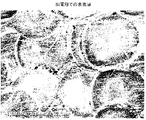
Si表面層のSi量が面の凹凸の性状に影響する点について述べたが、その一例を図25、図26に示す。
Si電極での同一処理条件での処理を時間毎に変えて行い、Si表面層の表面(図25)、及び、Si表面層の断面(図26)の様子を観察したものである。
すべての処理を処理条件一定で行なっているので、処理時間の比は発生した放電の回数の比とほぼ同じと考えてよい。すなわち、処理時間が短い場合には放電回数が少なく、処理時間が長い場合には放電の回数が多いことになる。(ただし、処理時間は休止時間などの条件により変わるため、同一放電パルス数を発生させるためには、休止時間が変化すれば必要な処理時間はかわる。)
図に示したSi表面層の処理時間は3分、4分、6分、8分である。図から以下のことが言える。The point that the amount of Si in the Si surface layer affects the surface irregularity is described. An example is shown in FIGS. 25 and 26.
The processing under the same processing conditions with the Si electrode was performed at different times, and the surface of the Si surface layer (FIG. 25) and the cross section of the Si surface layer (FIG. 26) were observed.
Since all processing is performed under constant processing conditions, the processing time ratio may be considered to be substantially the same as the ratio of the number of generated discharges. That is, when the processing time is short, the number of discharges is small, and when the processing time is long, the number of discharges is large. (However, since the processing time varies depending on conditions such as the pause time, the required processing time changes if the pause time changes in order to generate the same number of discharge pulses.)
The treatment times of the Si surface layer shown in the figure are 3, 4, 6, and 8 minutes. The following can be said from the figure.
処理時間が短い場合(3分)ではまだ面の凹凸が多く、表面に小さな突起状の部分が存在するのが観察される。(図示は省略するが、より短いとさらに突起状の部分が多く、処理時間3分が突起が目立たなくなってきている境界である)
処理時間を増していくと、これらの凹凸、突起が少なくなり平滑になっていく様子がわかる。When the treatment time is short (3 minutes), there are still many irregularities on the surface, and it is observed that small protrusions are present on the surface. (The illustration is omitted, but if it is shorter, there are more protruding parts, and the processing time of 3 minutes is the boundary where the protrusions are not noticeable)
It can be seen that as the processing time is increased, these irregularities and protrusions decrease and become smoother.
一方断面写真を見ると、処理時間3分から8分までの断面で、Si表面層の厚みはほとんど変化のないことがわかる。それぞれの被膜のSi量を分析すると、処理時間3分の被膜が約3wt%、処理時間4分の被膜が約6wt%、処理時間6分の被膜が約8wt%、処理時間8分の被膜が約6wt%であった。処理時間が短い場合にはSiが十分に表面層に入っていないが、ある程度処理時間が経過(この条件では4分)するとSiがほぼ十分に入り、面が平滑になることがわかった。
以上より、Siが少ないと面の平滑性が悪く、3wt%以上は必要であり、より望ましくは6wt%以上必要なことがわかる。(詳細は後述するが、耐食試験を行った結果、3分の試験片は多少は耐食の効果があるが腐食はした。4分、6分、8分は腐食しなかった。)On the other hand, the cross-sectional photograph shows that the thickness of the Si surface layer hardly changes in the cross section from the processing time of 3 minutes to 8 minutes. Analyzing the amount of Si in each film, the film with a treatment time of 3 minutes was about 3 wt%, the film with a treatment time of 4 minutes was about 6 wt%, the film with a treatment time of 6 minutes was about 8 wt%, and the film with a treatment time of 8 minutes About 6 wt%. When the treatment time was short, Si was not sufficiently contained in the surface layer, but it was found that when the treatment time passed to some extent (4 minutes under this condition), Si entered almost enough and the surface became smooth.
From the above, it can be seen that when the amount of Si is small, the smoothness of the surface is poor, 3 wt% or more is necessary, and more desirably 6 wt% or more is necessary. (Although details will be described later, as a result of the corrosion resistance test, the test piece of 3 minutes had some corrosion resistance but was corroded. It did not corrode for 4 minutes, 6 minutes and 8 minutes.)
上述の如く、表面の面粗さの低下するタイミングと、表面層のSi量が十分になるタイミングが一致することが明らかとなったが、この理由は以下のように考えている。
Siは溶融時の粘度が低い材料であることが知られている。処理の初期の状態はSiが十分に表面層に入っていないため、基材である鋼材の溶融粘度に近く、放電が発生することによる面の荒れが支配的になる。処理が進行して表面層のSi濃度が高くなると、溶融したときに材料が流れやすい状態になり、面が平滑になると考えられる。
この推察の説明図を図27に示す。
Siが入ることで面が平滑になり、Si表面層の性能が発揮されることがわかったので、処理時間をどのように決めるかという明確な指標が得られたことになる。As described above, it has been clarified that the timing at which the surface roughness of the surface is reduced coincides with the timing at which the Si amount of the surface layer becomes sufficient. The reason for this is considered as follows.
It is known that Si is a material having a low viscosity when melted. Since Si is not sufficiently contained in the surface layer in the initial state of the treatment, it is close to the melt viscosity of the steel material as the base material, and surface roughness due to the occurrence of discharge becomes dominant. When the treatment progresses and the Si concentration in the surface layer increases, the material is likely to flow when melted and the surface is thought to be smooth.
An explanatory diagram of this inference is shown in FIG.
Since it has been found that the surface becomes smooth when Si enters and the performance of the Si surface layer is exerted, a clear indicator of how to determine the processing time is obtained.
面の粗さの観点から、処理時間について論じたが、処理時間と面粗さと皮膜性能の関係についてより詳細に確認した。皮膜性能としては、ここでは、耐食性の評価のみを示す。
図28は冷間ダイス鋼SKD11に対する処理時間を変化させた際の処理時間と面粗さ(Rz)との関係を表したグラフである。
ここで、処理条件としては10mm×10mmの面積のSi電極を用いて10mm×10mmの面積に、電流パルスの電流値ie=8A、パルス幅te=8μs、放電休止時間to=64μsの設定、すなわち、パルスのエネルギーが約60A・μsの条件とし、処理時間は、2分、3分、4分、6分、8分、16分で行なった。
また、図中にそれぞれ(一部)の処理時間の試験片を王水に浸漬して腐食試験を行なった後の電子顕微鏡(SEM)写真を載せてある。The processing time was discussed from the viewpoint of surface roughness, but the relationship between the processing time, surface roughness, and film performance was confirmed in more detail. Here, only the evaluation of corrosion resistance is shown as the film performance.
FIG. 28 is a graph showing the relationship between the processing time and the surface roughness (Rz) when the processing time for the cold die steel SKD11 is changed.
Here, as processing conditions, using a Si electrode having an area of 10 mm × 10 mm, an area of 10 mm × 10 mm, a current pulse current value ie = 8 A, pulse width te = 8 μs, and discharge rest time to = 64 μs are set. The pulse energy was about 60 A · μs, and the treatment time was 2 minutes, 3 minutes, 4 minutes, 6 minutes, 8 minutes, and 16 minutes.
Moreover, the electron microscope (SEM) photograph after putting the test piece of each (part) processing time into aqua regia and performing a corrosion test in the figure is mounted.
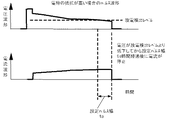
処理時間2分では表面が腐食して表面層が全く見られなくなった。3分では、表面層が残るものの、腐食が激しく進んでおり、表面はぼろぼろの状態になった。処理時間4分、6分、8分は表面層部分の腐食は見られなかった。16分は一部に腐食が進んだ痕が見られた。処理時間が長くなるに従い、一旦面粗さが良くなる理由は前述のとおりであるが、さらに処理時間が長くなった場合に面粗さが悪くなる理由は、放電を長時間継続することで、工作物が除去されることにより工作物内部の析出物が現れてくるのではないかと推測しているが詳細はわからない点も多い。 In the treatment time of 2 minutes, the surface was corroded and the surface layer was not seen at all. In 3 minutes, although the surface layer remained, the corrosion progressed violently and the surface was in a shabby state. Corrosion of the surface layer portion was not observed at the treatment times of 4, 6, and 8 minutes. For 16 minutes, there was a trace of partial corrosion. The reason why the surface roughness once improves as the processing time becomes longer is as described above, but the reason that the surface roughness becomes worse when the processing time becomes longer is that the discharge is continued for a long time, Although it is speculated that the deposit inside the workpiece will appear when the workpiece is removed, there are many points where details are unknown.
図28からわかるように、この処理条件の場合には、処理時間が6分程度で面粗さが低下しており(この場合極小値を持っており)、耐食性も高い。
耐食性が高い範囲は処理時間が4分程度からであり、このときの面粗さは、おおよそ極小値である6分の時の面粗さの1.5倍であった。
また、図示はしていないが、処理時間が長い場合には、12分程度までは耐食性が十分にあり、そのときの面粗さも6分のときの面粗さの約1.5倍であった。
したがって、Si表面層が性能を発揮するためには、面粗さが低下した時点の面粗さの1.5倍程度までの範囲にあること、これは処理時間でいうと面粗さが低下したときまでの処理時間の1/2から2倍の範囲にあることが必要であるということになる。
この現象は、工作物材料によっても異なっており、SUS304のような材料では、面粗さが一旦下がってから粗くなる現象があまり見られない。また粗くなる場合でも析出物が現れるというよりは、電極消耗、工作物の除去により全体としてうねりがでてくるためのようである。As can be seen from FIG. 28, in the case of this processing condition, the processing time is about 6 minutes, the surface roughness is reduced (in this case, it has a minimum value), and the corrosion resistance is also high.
The range where the corrosion resistance is high is from the processing time of about 4 minutes, and the surface roughness at this time is 1.5 times the surface roughness at the time of 6 minutes, which is a minimum value.
Although not shown, when the processing time is long, the corrosion resistance is sufficient up to about 12 minutes, and the surface roughness at that time is about 1.5 times the surface roughness at 6 minutes.
Therefore, in order for the Si surface layer to exhibit its performance, it is in a range up to about 1.5 times the surface roughness at the time when the surface roughness is reduced, which is when the surface roughness is reduced in terms of processing time. It is necessary to be in the range of 1/2 to 2 times the processing time up to.
This phenomenon differs depending on the workpiece material. With a material such as SUS304, a phenomenon in which the surface roughness decreases once after the surface roughness is reduced is rarely observed. In addition, even when the surface becomes rough, the precipitate appears rather than appears as a whole due to electrode wear and removal of the workpiece.
図29にSUS304の場合のグラフを示す。処理条件は図28のSKD11の場合と同一である。
図よりわかるようにSUS304の場合には面粗さが低下した8分程度が最適な(処理時間が短く、皮膜性能が得られる)処理時間である。6分程度でもそれなりの耐食性は得られており、そのときの面粗さは8分の時の面粗さの1.5倍程度であった。SUS304の場合には、処理時間が長くなってもSKD11のように急激に面粗さが上昇する現象は見られなかった。また、処理時間が長くなっても耐食性が急激に悪化するという現象も生じなかった。しかし、処理時間が長くなると、処理部すなわち表面層が形成されている部分の凹みが大きくなり、例えば処理時間12分では、凹み量が10μm程度になり、金型として使用する限界程度の精度になってしまった。
したがって、面粗さが悪化しない材料の場合には処理時間が長くてもよいかというとそのようなことはなく、やはり、面粗さが低下した最適値の約2倍程度までが処理時間としてふさわしいということができる。FIG. 29 shows a graph for SUS304. The processing conditions are the same as in the case of SKD11 in FIG.
As can be seen from the figure, in the case of SUS304, the optimum processing time (short processing time and film performance can be obtained) is about 8 minutes when the surface roughness is reduced. Corresponding corrosion resistance was obtained even at about 6 minutes, and the surface roughness at that time was about 1.5 times the surface roughness at 8 minutes. In the case of SUS304, even when the processing time was long, the phenomenon that the surface roughness rapidly increased like SKD11 was not observed. Further, the phenomenon that the corrosion resistance deteriorates rapidly even when the treatment time is long did not occur. However, as the processing time becomes longer, the dent in the processing portion, that is, the portion where the surface layer is formed becomes larger. It is had.
Therefore, in the case of a material whose surface roughness does not deteriorate, there is no such thing as whether the processing time may be long, and the processing time is up to about twice the optimum value where the surface roughness is lowered. It can be said that it is appropriate.
図28のような面粗さの推移を示す材料としては、SKD11以外に、S-C材(S40C、S50Cなど)、高速度工具鋼SKH51等がある。
また、図29のような推移を示す材料としては、SUS630等がある。As materials showing the transition of the surface roughness as shown in FIG. 28, SC material (S40C, S50C, etc.), high-speed tool steel SKH51, etc. are available in addition to SKD11.
In addition, as a material showing the transition as shown in FIG. 29, there is SUS630 or the like.
なお、以上の説明では処理時間で説明したが、処理の時間そのものが本質的なものではないことはいうまでない。本来は単位面積あたりどれだけの放電のパルスを発生させたか、どれだけのエネルギーを投入したかが重要である。ちなみに図28で説明した処理条件では、毎秒5000から6000回の放電を発生させる条件であり、適切な処理時間といっている6分では、
5000〜6000回/秒 × 60秒/分 × 6分
の回数の放電が発生していることになる。
処理条件が一定の場合には、放電の回数の比は処理時間の比に一致するが、処理条件を途中で変更する場合には、処理時間での管理はあまり意味がなくなる。この場合でも放電の発生回数による管理は正しい。In the above description, the processing time has been described, but it goes without saying that the processing time itself is not essential. Originally, it is important how many discharge pulses are generated per unit area and how much energy is supplied. Incidentally, the processing conditions described in FIG. 28 are conditions that generate 5000 to 6000 discharges per second. In 6 minutes, which is an appropriate processing time,
5000 to 6000 times / second x 60 seconds /
The number of times of discharge has occurred.
When the processing conditions are constant, the ratio of the number of discharges coincides with the processing time ratio. However, when the processing conditions are changed in the middle, management at the processing time becomes less meaningful. Even in this case, management based on the number of occurrences of discharge is correct.
以上のように、面粗さが低下するタイミングは工作物にSiが適度に入るタイミングと一致し、しかも、皮膜の性能が発揮されるタイミングとも一致することが明確となった。具体的なタイミングを決める方法は、以下のようなことが考えられる。
1)実際に処理を行ないながら処理を終了するタイミングをその場で決める場合には、定期的に処理面の面粗さを測定し、順に面粗さが低下するのを確認しながら処理を進める。測定しても、面粗さが低下しなくなった時点で処理を終了する。As described above, it has been clarified that the timing at which the surface roughness decreases coincides with the timing at which Si appropriately enters the workpiece, and also coincides with the timing at which the performance of the film is exhibited. The following can be considered as a method for determining the specific timing.
1) When determining the timing to end processing while actually performing processing, measure the surface roughness of the processing surface periodically and proceed while confirming that the surface roughness decreases in order. . Even if the measurement is performed, the process is terminated when the surface roughness does not decrease.
2)あらかじめ事前に処理時間を決めてから処理を行なう場合には、基準とする電極を用意し、図28、図29のように処理時間と面粗さとの関係を確認し、面粗さが低下した時間を基準とした処理面積での適切な処理時間とする。実際の加工の際に、基準の電極と処理面積が異なる場合には、面積を換算した処理時間を算出しておき(同一の処理条件であれば、面積に比例した時間とする。処理条件を変更して放電の周期を変える場合には、単位面積当たりの放電の回数が同等程度になるように処理時間を決定する)、その処理時間で処理を行なう。このような準備は勿論、加工の都度行なうのではなく、あらかじめデータを取得しておき、実際の処理の際にすぐに利用できるようにしておくことが望ましいのはいうまでない。 2) When processing after determining the processing time in advance, prepare a reference electrode and check the relationship between the processing time and surface roughness as shown in FIGS. An appropriate processing time in the processing area based on the reduced time is set. When the processing area is different from the reference electrode during actual processing, a processing time converted from the area is calculated (if the processing conditions are the same, the time is proportional to the area. When changing and changing the discharge cycle, the processing time is determined so that the number of discharges per unit area is approximately the same), and the processing is performed at that processing time. It goes without saying that such preparation is not performed every time processing is performed, but it is desirable that data be acquired in advance and used immediately in actual processing.
3)処理時間をあらかじめ決めるのではなく、2)のところで取ったデータから、適切な処理時間の場合に、電極がどれだけ消耗するかをあらかじめ把握しておく。実際の処理の際には、電極がその消耗量に達するまで処理を継続する。 3) Instead of predetermining the processing time, know in advance how much the electrode will be consumed in the case of an appropriate processing time from the data taken in 2). In actual processing, the processing is continued until the electrode reaches its consumption.
以上、大まかに処理時間を決定する3つの方法について示したが、この組合せや面積が変わる場合などにいろいろなバリエーションが考えられる。面粗さが小さくなった点が表面層として適した状態であることは述べたとおりであるが、処理を進めて面粗さが最小値をとるところがあるが、被膜として適している面粗さはその最小値の1.5倍程度の面粗さくらいまでであり、処理時間ではそのときの処理時間の半分から2倍程度の範囲であることが望ましい。それを大きく超えるとSiの濃度が少なかったり、あるいは、析出物が表面に現れたりして、耐食性・耐エロージョン性が低下する。また、処理時間が長い場合には、処理部の凹みが大きくなり実用に耐えなくなる。以上の内容をこれは同一処理条件で処理を行っている場合では、面粗さが低下した処理時間をT0とすると、望ましい処理時間の範囲は
1/2T0 ≦ T ≦ 2T0
ということができる。The three methods for roughly determining the processing time have been described above, but various variations are conceivable when this combination or area changes. As described above, the point where the surface roughness is reduced is suitable for the surface layer, but there are places where the surface roughness reaches the minimum value by proceeding with the processing, but the surface roughness is suitable as a coating. Is about 1.5 times the minimum surface roughness, and the processing time is preferably in the range of about half to twice the processing time at that time. On the other hand, the Si concentration is low or precipitates appear on the surface, and the corrosion resistance and erosion resistance deteriorate. In addition, when the processing time is long, the dent of the processing unit becomes large and cannot be practically used. In the case where processing is performed under the same processing conditions as described above, assuming that the processing time when the surface roughness is reduced is T0, the desirable processing time range is
1 / 2T0 ≤ T ≤ 2T0
It can be said.
また、今までに述べてきたことの繰り返しになるが、放電パルス数を計数する手段を備え、面粗さが低下した(最適な処理時間)放電パルス数をN0とすると、望ましい放電パルス幅の範囲Nは、
1/2N0 ≦ N ≦ 2N0
ということになる。
3次元形状の金型や部品に処理を行う場合等、部分により処理時間が異なるということも起こりえるので注意する必要がある。In addition, as described above up to now, a means for counting the number of discharge pulses is provided, and assuming that the number of discharge pulses with reduced surface roughness (optimum processing time) is N0, a desired discharge pulse width is obtained. Range N is
1 / 2N0 ≤ N ≤ 2N0
It turns out that.
It should be noted that the processing time may vary depending on the part, such as when processing a three-dimensional mold or component.
なお、これまで面粗さの推移について述べてきたが、ここで言っている面粗さは、放電により形成される面としての粗さのことである。すなわち、元の基材の面粗さはある程度以上のよい面であることが前提になっている。少なくとも放電が発生することでできる凹凸よりも元の基材の面粗さが小さいことが前提として説明を行ってきたことを述べておく。
つまり、議論していた内容は、放電が発生することで、面に放電による凹凸が形成されるが、Siが適切な量基材中に入るに従い放電により形成される凹凸が小さくなるということである。
通常の金型に使用する面や、精度の高い部品の場合にはこの条件は当てはまり、これまで述べてきたように、面粗さが一旦大きくなった後、小さくなるという現象でよいが、元々の基材の面粗さが粗い場合には、当然ながら、面粗さ計で測定した値だけで見ると、一旦面粗さが大きくなった後、小さくなるという推移にはならなくなる。この場合には、これまで述べてきたことは同様に成り立つことはいうまでなく、ただ、面粗さとして述べてきた値にある補正が必要ということである。補正とは、元々の基材の面粗さを差し引くことが必要であるということであり、実用上は、あらかじめ別の面粗さの細かい基材(条件を出すための試験片)で面粗さが大きくなった後、小さくなるタイミングを見つけておき、それ相当の処理時間で処理を行うということになる。In addition, although transition of surface roughness has been described so far, the surface roughness mentioned here is roughness as a surface formed by discharge. That is, it is assumed that the surface roughness of the original base material is a good surface of a certain degree or more. It will be described that the description has been made on the premise that the surface roughness of the original base material is smaller than the unevenness that can be generated at least by the occurrence of discharge.
In other words, the content of the discussion was that when discharge occurs, irregularities due to discharge are formed on the surface, but as the Si enters the base material, the irregularities formed by discharge become smaller. is there.
In the case of a surface used for a normal mold or a highly accurate part, this condition is applicable, and as described above, the phenomenon that the surface roughness once increases and then decreases may be used. When the surface roughness of the base material is rough, naturally, when only the value measured with the surface roughness meter is used, the surface roughness once increases and then does not change. In this case, it goes without saying that what has been described so far holds true, but it is only necessary to make a correction at the value described as the surface roughness. The correction means that it is necessary to subtract the surface roughness of the original base material. In practice, the surface roughness is measured in advance with a base material with a different surface roughness (a test piece for determining conditions). After the time becomes larger, the timing of becoming smaller is found, and the processing is performed in a corresponding processing time.
ところで、耐エロージョン性能として、本発明によるSi表面層が優れている理由については以下のように考えている。耐エロージョン性は、一般的には硬さと相関が強いといわれている。しかし、前述の評価結果からもわかるように、硬さだけでは説明のつかない点も多い。硬さ以外の要素としては、表面の性状が影響しており、粗い面より、より鏡面に近いほうが、耐エロージョン性が上がることがわかってきている。Si表面層で耐エロージョン性が優れている理由としても面の性状が挙げられる。Si表面層は硬さが600HV〜1100HVとある程度硬く、面の性状が滑らかな面になっている。このことが耐エロージョン性に影響していると考えている。 By the way, the reason why the Si surface layer according to the present invention is excellent as the erosion resistance is considered as follows. The erosion resistance is generally said to have a strong correlation with hardness. However, as can be seen from the above evaluation results, there are many points that cannot be explained only by hardness. As an element other than hardness, the surface properties have an influence, and it has been found that the erosion resistance is improved closer to a mirror surface than a rough surface. The surface properties can be cited as the reason why the erosion resistance is excellent in the Si surface layer. The Si surface layer has a hardness of 600 HV to 1100 HV to some extent, and has a smooth surface. This is thought to affect the erosion resistance.
さらに、通常の硬い被膜(例えば前述のTiC被膜やPVD、CVDなどによる硬質被膜)は靭性が低く、わずかな変形により被膜が破壊されてしまうのに対し、Si表面層は靭性が高く変形を加えてもクラックなどが入りにくい性質を持っていることも高い耐エロージョン性の原因の1つであると考えている。
さらに、Si表面層の結晶構造にも影響していると考えている。本発明の範囲の条件で形成したSi表面層のX線回折結果を図30に示す。
図では基材のSUS630とその上にSi表面層を形成した場合の回折像を示している。
Si表面層の回折像を見るとわかるように基材のピークは見えるものの、非晶質(アモルファス)組織の形成が認められる幅広いバックグラウンドが観察される。すなわちSi表面層は非晶質になっており、そのため通常の材料で発生しやすい結晶粒界での破壊がおきにくいと考えることができる。In addition, ordinary hard coatings (for example, the above-mentioned TiC coating, hard coating by PVD, CVD, etc.) have low toughness, and the coating is destroyed by slight deformation, whereas the Si surface layer has high toughness and deformation. However, it is considered that one of the causes of high erosion resistance is that it has a property that cracks and the like are difficult to enter.
Further, it is considered that the crystal structure of the Si surface layer is also affected. The X-ray diffraction results of the Si surface layer formed under the conditions within the scope of the present invention are shown in FIG.
The figure shows a diffraction image in the case of forming SUS630 as a base material and a Si surface layer thereon.
As can be seen from the diffraction pattern of the Si surface layer, although the peak of the substrate is visible, a wide background in which formation of an amorphous structure is recognized is observed. In other words, the Si surface layer is amorphous, so that it can be considered that the fracture at the crystal grain boundaries, which are likely to occur with ordinary materials, hardly occurs.
ところで、本明細書中で述べているSi表面層は、Siの含有量が3〜11wt%含むSi濃化層をさしており、特許文献1で示されるような3μmの層とは異なるものである。
該定義について詳述すると、特許文献1に示される層とは、光学顕微鏡での観察により層の厚さを特定しているため、図31に示される如く、本明細書で述べているようなSi表面層と、放電表面処理による熱影響層を含んだ厚みを膜厚の層と定義している。By the way, the Si surface layer described in this specification refers to a Si concentrated layer containing 3 to 11 wt% of Si, and is different from a 3 μm layer as disclosed in
The definition will be described in detail. The layer shown in
実施の形態2.
実施の形態1ではSiを電極とした場合について説明したが、同じ現象がSiに他の材料を混合した電極についても当てはまる。Si電極による表面層は、耐食性・耐エロージョン性などの性質が得られるが、例えば硬さについては、800HV程度であり、それほど硬質材料でもない。より硬さを要求されるような用途には、硬い材料を混合することで、硬さを上げることも必要になる。
In the first embodiment, the case where Si is used as the electrode has been described. However, the same phenomenon applies to an electrode obtained by mixing other materials with Si. The surface layer made of the Si electrode can obtain properties such as corrosion resistance and erosion resistance. For example, the hardness is about 800 HV, which is not a very hard material. For applications that require higher hardness, it is also necessary to increase the hardness by mixing hard materials.
本実施の形態では硬質材料の粉末として、TiC粉を用いて説明する。
TiC粉とSi粉とを少しずつ割合を変化させて混合したTiC+Si混合粉を用いて放電表面処理用電極を作成し、電極と被処理材(基材)との間に電圧を印加して放電を発生させ、基材に表面層を形成した。In the present embodiment, TiC powder will be described as the hard material powder.
An electrode for discharge surface treatment is created using TiC + Si mixed powder in which the ratio of TiC powder and Si powder is mixed little by little, and a voltage is applied between the electrode and the material to be processed (base material) for discharge. And a surface layer was formed on the substrate.
図32は、電極へのSi混合比(重量%)と表面層の面粗さの関係を示したものである。
TiC粉に、少しずつ割合を変化させてSi粉を混合して作成したTiC+Si電極で機械構造用炭素鋼S45Cに処理した皮膜の面粗さを測定した結果、電極へのSi混合比が大きくなるほど、表面層の面粗さは小さくなっている。
なお、本実施の形態では、表面層の面粗さは2〜6μmRzの範囲で変化している。FIG. 32 shows the relationship between the Si mixing ratio (wt%) to the electrode and the surface roughness of the surface layer.
As a result of measuring the surface roughness of the film processed on the carbon steel for mechanical structure S45C with a TiC + Si electrode prepared by mixing the Si powder by changing the ratio to the TiC powder little by little, the Si mixing ratio to the electrode increases. The surface roughness of the surface layer is small.
In the present embodiment, the surface roughness of the surface layer changes in the range of 2 to 6 μm Rz.
図33は、電極へのSi混合比(重量%)と表面層の硬さの関係を示したものである。
TiC粉に、少しずつ割合を変化させてSi粉を混合して作成したTiC+Si電極で機械構造用炭素鋼S45Cに処理した表面層の硬さを測定した結果、Si混合比が60重量%以下では、電極へのSi混合比が大きくなるほど、表面層の硬さは小さくなっている。
また、Si混合比が60重量%以上では表面層の硬さはほとんど変わっていない。なお、本実施の形態では、表面層の硬さは800〜1700HVの範囲で変化している。FIG. 33 shows the relationship between the Si mixing ratio (wt%) to the electrode and the hardness of the surface layer.
As a result of measuring the hardness of the surface layer processed into carbon steel for mechanical structure S45C with a TiC + Si electrode made by mixing Si powder by changing the ratio to TiC powder little by little, when the Si mixing ratio is 60% by weight or less The hardness of the surface layer decreases as the Si mixing ratio to the electrode increases.
Further, when the Si mixing ratio is 60% by weight or more, the hardness of the surface layer hardly changes. In the present embodiment, the hardness of the surface layer changes in the range of 800 to 1700 HV.
なお、TiC粉とSi粉とを少しずつ割合を変化させて混合して作成したTiC+Si電極で機械構造用炭素鋼S45Cに処理した表面層のSi濃度を測定したところ、電極内のSi重量比と表面層のSi濃度の関係は図34の通りとなった。
電極内のSi重量比が大きくなると、表面層のSi濃度も大きくなっている。
なお、ここで言うSi量は、エネルギー分散型X線分光分析法(EDX)により、表面層表面方向から測定した値であり、測定条件は、加速電圧15.0kV,照射電流1.0nAである。In addition, when the Si concentration of the surface layer processed into the carbon steel for mechanical structure S45C was measured with a TiC + Si electrode prepared by mixing the TiC powder and the Si powder while changing the ratio little by little, the Si weight ratio in the electrode and The relationship of the Si concentration of the surface layer is as shown in FIG.
As the Si weight ratio in the electrode increases, the Si concentration in the surface layer also increases.
The amount of Si referred to here is a value measured from the surface layer surface direction by energy dispersive X-ray spectroscopy (EDX), and the measurement conditions are an acceleration voltage of 15.0 kV and an irradiation current of 1.0 nA.
このように、電極のSi混合比が多くなるほど、表面層に含まれるSi濃度は大きくなり、その結果、表面層の面粗さは小さくなっていると考えられるが、そのメカニズムを調査するため、表面層の表面をSEMで観察を行った。
その結果、Si濃度が大きくなるにつれて、表面層にクラックなどの欠陥が少なくなり、また放電痕一つ一つの盛り上がりが小さくなっていることが観察された。Thus, as the Si mixing ratio of the electrode increases, the Si concentration contained in the surface layer increases, and as a result, the surface roughness of the surface layer is considered to decrease, but in order to investigate the mechanism, The surface of the surface layer was observed with SEM.
As a result, it was observed that as the Si concentration was increased, defects such as cracks were reduced in the surface layer, and the rise of each discharge trace was reduced.
以降、各混合比(重量比)の電極を、例えばTiC粉末:Si粉末=8:2であればTiC+Si(8:2)電極、TiC粉末:Si粉末=5:5であればTiC+Si(5:5)電極のように表記する。 Thereafter, electrodes of each mixing ratio (weight ratio) are, for example, TiC + Si (8: 2) electrode if TiC powder: Si powder = 8: 2, TiC + Si (5: 5 if TiC powder: Si powder = 5: 5). 5) Express as an electrode.
一例として、図35〜図39に、比較としてTiC電極で処理した表面、TiC+Si(8:2)電極、TiC+Si(7:3)電極、TiC+Si(5:5)電極で処理した表面、比較としてSi電極で処理した表面のSEM観察結果を示す。
TiC電極での処理面では、クラックなどの欠陥が非常に多く、放電痕一つ一つの盛り上がりが大きく、TiC+Si(8:2)電極、TiC+Si(7:3)電極、TiC+Si(5:5)電極の順に、処理面にクラックなどの欠陥は少なくなり、放電痕一つ一つの盛り上がりが小さくなり、Si電極での処理面ではクラックなどの欠陥は全く見られず、放電痕一つ一つの盛り上がりが非常に小さいことが観察できる。As an example, FIGS. 35 to 39 show a surface treated with a TiC electrode for comparison, a surface treated with a TiC + Si (8: 2) electrode, a TiC + Si (7: 3) electrode, a TiC + Si (5: 5) electrode, and a comparison with Si. The SEM observation result of the surface processed with the electrode is shown.
On the treated surface of the TiC electrode, there are very many defects such as cracks, and each discharge trace has a large rise, TiC + Si (8: 2) electrode, TiC + Si (7: 3) electrode, TiC + Si (5: 5) electrode In this order, defects such as cracks are reduced on the treated surface, and the rise of each discharge trace is reduced, and defects such as cracks are not seen at all on the treated surface of the Si electrode, and each discharge trace is raised. It can be observed that it is very small.
ここで、表面層に含まれるSi濃度は大きくなることで、放電痕一つ一つの盛り上がりが小さくなるメカニズムは次のように考えている。
すなわち、Siは粘性率が他の金属に比べて小さい(0.94mN・s/m2)ため、Siが混入されることで、放電により溶融した電極材質が基材に移行して凝固する際に、溶融部分のSi濃度が大きくなることで、溶融部分の粘性率が小さくなり、より扁平に拡がりながら凝固するため、盛り上がりが小さくなると考えられる。
図27で説明したように、Siが溶融したときにTiCも含めて流れやすい状態になり平滑な面を形成すると考えられる。Here, the mechanism of reducing the rise of each discharge trace by increasing the Si concentration contained in the surface layer is considered as follows.
That is, since Si has a smaller viscosity than other metals (0.94 mN · s / m 2 ), when Si is mixed, the electrode material melted by the discharge moves to the base material and solidifies. The increase in the Si concentration in the molten part decreases the viscosity of the molten part, and solidifies while spreading more flatly.
As described with reference to FIG. 27, it is considered that when Si is melted, TiC is easily flowed and a smooth surface is formed.
TiC粉とSi粉とを少しずつ割合を変化させて混合して作成したTiC+Si電極で処理した表面層に対して、X線回折測定を行ったところ、TiCの回折ピークが確認され、電極材料時のTiCは、放電表面処理後もTiCとして表面層に存在していることが分かった。なお、Ti単体の回折ピークは確認されない。
一例として、図40にTiC+Si(8:2)電極、TiC+Si(7:3)電極、TiC+Si(5:5)電極で成膜した皮膜のXRD回折測定結果を示す。When the X-ray diffraction measurement was performed on the surface layer treated with the TiC + Si electrode prepared by mixing the TiC powder and Si powder while changing the ratio little by little, the TiC diffraction peak was confirmed and the electrode material was The TiC was found to be present in the surface layer as TiC even after the discharge surface treatment. In addition, the diffraction peak of Ti simple substance is not confirmed.
As an example, FIG. 40 shows an XRD diffraction measurement result of a film formed using a TiC + Si (8: 2) electrode, a TiC + Si (7: 3) electrode, and a TiC + Si (5: 5) electrode.
一方、電極のSi混合比が大きくなる、すなわち電極のTiC混合比が小さくなると、表面層のTiCのいずれの回折ピークの積分強度も小さくなっている。
また、図41は、電極へのSi混合比と皮膜のTi濃度の関係を示している。
電極のSi混合比が大きくなる、すなわち電極のTiC混合比が小さくなると、表面層のTi濃度は小さくなる。XRD回折測定結果より、Ti単体のピークは見られないため、電極時のTiCは一部放電表面処理時に分解している可能性はあるが、大部分はそのままTiCの状態で表面層内に存在していると考えられる。
以上より、電極のSi混合比が大きくなる、すなわち電極のTiC混合比が小さくなると、表面層のTiC濃度も相対的に小さくなっていると推察される。On the other hand, when the Si mixing ratio of the electrode increases, that is, when the TiC mixing ratio of the electrode decreases, the integrated intensity of any diffraction peak of TiC in the surface layer decreases.
FIG. 41 shows the relationship between the Si mixture ratio to the electrode and the Ti concentration of the film.
When the Si mixing ratio of the electrode increases, that is, when the TiC mixing ratio of the electrode decreases, the Ti concentration of the surface layer decreases. From the XRD diffraction measurement results, there is no peak of Ti alone, so there is a possibility that TiC at the time of electrode is partially decomposed during discharge surface treatment, but most of it exists in the surface layer in the state of TiC as it is it seems to do.
From the above, it can be inferred that the TiC concentration of the surface layer is also relatively reduced when the Si mixture ratio of the electrode is increased, that is, when the TiC mixture ratio of the electrode is decreased.
以上より、電極へのSi混合比が大きくなると、表面層において、硬質のTiC濃度が小さくなり、その結果表面層硬さが小さくなると考えられる。
一方、処理表面には前述の定量分析の通り、Si元素が数〜数十重量%程度存在しているにもかかわらず、X線回折測定の結果、いずれの表面層もSiの結晶の回折ピークは確認できなかった。このことから、Si単体は基材成分と合金を形成している、もしくは非晶質状態になっていると考えられる。From the above, it is considered that when the Si mixing ratio to the electrode is increased, the hard TiC concentration is decreased in the surface layer, and as a result, the surface layer hardness is decreased.
On the other hand, as shown in the quantitative analysis described above, although the Si element is present in the range of several to several tens of weight%, as a result of X-ray diffraction measurement, all surface layers have diffraction peaks of Si crystals. Could not be confirmed. From this, it is considered that Si alone forms an alloy with the base material component or is in an amorphous state.
電極にSiを混合することで皮膜のSi濃度を大きくすることの効果をまとめると、図42のようになる。
すなわち、電極へのSi混合比が小さいとき、放電表面処理による溶融部(皮膜)にクラックなどの欠陥が非常に多く、放電痕一つ一つの盛り上がりが大きい。
一方、Si混合比が大きくなるにつれて、クラックなどの欠陥は少なくなり、放電痕一つ一つの盛り上がりは小さくなる。
また、皮膜は、Si単体と基材成分が合金を形成している、もしくは非晶質状態になっていると推察され、そこにTiCが分散している皮膜形態になっていると推察している。
なお、皮膜は一部基材高さよりも低い位置まで拡散している。表面層は拡散部分まで合わせて、5〜10μm程度である。FIG. 42 summarizes the effects of increasing the Si concentration of the film by mixing Si with the electrode.
That is, when the Si mixture ratio to the electrode is small, the melted part (film) by the discharge surface treatment has a lot of defects such as cracks, and the discharge marks are greatly raised.
On the other hand, as the Si mixing ratio increases, defects such as cracks decrease, and the rise of each discharge trace decreases.
In addition, it is inferred that the film is in the form of a film in which the simple substance of Si and the base material component form an alloy or are in an amorphous state, and TiC is dispersed therein. Yes.
In addition, the coating has diffused to a position lower than the base material height. The surface layer is about 5 to 10 μm in total including the diffusion part.
次に、TiC粉とSi粉とを少しずつ割合を変化させて混合して作成したTiC+Si電極で処理した表面層について、耐エロージョン性について各皮膜の評価を行った。
ここでは、基材はSUS630(H1075)とした。
また、耐エロージョン性はウォータージェットを表面層に当てることにより評価した。
なお、耐エロージョン性は、一般的には硬さと相関が強いと言われているが、前述のように硬さだけでは説明がつかない点も多く、硬さ以外の要素としては、表面の性状が影響しており、粗い面より、より平滑な面の方が、耐エロージョン性が上がることが分かってきている。
Si電極で処理した表面層では高い耐エロージョン性が得られることが分かっていたが、今回評価した結果、TiC電極にSiを5重量%以上混入した電極で処理した表面層で耐エロージョン性の向上が現れ始めた。
なお、5重量%程度では表面に欠陥が多少存在していることから評価にバラツキが見られた。そこで、さらに混入比を大きくすると、10重量%以上で十分な効果を付与することができ、より望ましくは20重量%以上混入した方がよい。20重量%以上混入した場合、評価にばらつきもなく、高い耐エロージョン性を有していた。Next, each coating was evaluated for erosion resistance with respect to the surface layer treated with the TiC + Si electrode prepared by mixing the TiC powder and the Si powder while changing the ratio little by little.
Here, the base material was SUS630 (H1075).
The erosion resistance was evaluated by applying a water jet to the surface layer.
In addition, erosion resistance is generally said to have a strong correlation with hardness. However, as described above, there are many points that cannot be explained only by hardness, and factors other than hardness include surface properties. It has been found that a smoother surface has a higher erosion resistance than a rough surface.
Although it was known that high erosion resistance was obtained with the surface layer treated with the Si electrode, as a result of evaluation this time, the erosion resistance was improved with the surface layer treated with an electrode in which 5% by weight or more of Si was mixed in the TiC electrode. Began to appear.
In addition, when the weight was about 5% by weight, there were some defects on the surface, and the evaluation was not uniform. Therefore, if the mixing ratio is further increased, a sufficient effect can be imparted at 10% by weight or more, and more desirably 20% by weight or more should be mixed. When 20% by weight or more was mixed, the evaluation had no variation and had high erosion resistance.
なお、このように、高い耐エロージョン性を有しているのは、以下の点が複合的に効果を及ぼしていると考えている。
・表面層が非晶質になっていることから、粒界からの破壊が起こりにくい
・TiCが分散していることで、高硬度になっている
・Siが混入されることで、平滑になっているIn addition, it is considered that the following points exert the effect in combination as having high erosion resistance.
・ Because the surface layer is amorphous, breakage from the grain boundary is unlikely to occur. ・ High hardness due to dispersion of TiC. ・ Smoothness by mixing Si. ing
例として、TiC+Si(8:2)電極、TiC+Si(7:3)電極、TiC+Si(5:5)電極で処理した表面層に対して、80MPaのウォータージェットを1hr噴射した後の表面状態を観察した結果を図43に示す。
比較として、基材のみ、TiC電極での表面層、Si電極での表面層での結果も示している。基材のみでは大きく損傷が発生し、TiC電極での処理面でも損傷が発生している。一方、TiC+Si(8:2)電極、TiC+Si(7:3)電極、TiC+Si(5:5)電極で処理したいずれの皮膜において損傷は発生していない。As an example, the surface state of a surface layer treated with a TiC + Si (8: 2) electrode, a TiC + Si (7: 3) electrode, and a TiC + Si (5: 5) electrode after spraying an 80 MPa water jet for 1 hr was observed. The results are shown in FIG.
As a comparison, the results for only the base material, the surface layer with the TiC electrode, and the surface layer with the Si electrode are also shown. A large amount of damage is caused only by the base material, and damage is also caused on the treated surface of the TiC electrode. On the other hand, no damage occurred in any of the films treated with the TiC + Si (8: 2) electrode, the TiC + Si (7: 3) electrode, and the TiC + Si (5: 5) electrode.
次に、耐食性について各表面層の評価を行った。ここでは、基材はSUS316とした。Si電極で処理した表面層では高い耐食性が得られることが知られているが、TiC電極にSiを5重量%以上混入した電極で処理した表面層において高い耐食性を有していた。
なお、5重量%程度では表面に欠陥が多少存在していることから評価にバラツキが見られた。そこで、さらに混入比を大きくすると、10重量%以上で十分な効果を付与することができ、より望ましくは10重量%以上混入した方がよい。20重量%以上混入した場合、評価にばらつきもなく、高い耐食性を有していた。
図44は、電極へのSi混合比と耐食性の関係を模式的に示した図である。Next, each surface layer was evaluated for corrosion resistance. Here, the base material was SUS316. The surface layer treated with the Si electrode is known to have high corrosion resistance. However, the surface layer treated with the electrode in which 5 wt% or more of Si is mixed in the TiC electrode has high corrosion resistance.
In addition, when the weight was about 5% by weight, there were some defects on the surface, and thus there was variation in evaluation. Therefore, if the mixing ratio is further increased, a sufficient effect can be imparted at 10% by weight or more, and more desirably 10% by weight or more should be mixed. When 20% by weight or more was mixed, the evaluation had no variation and had high corrosion resistance.
FIG. 44 is a diagram schematically showing the relationship between the Si mixture ratio to the electrode and the corrosion resistance.
なお、このように、高い耐食性を有しているのは、以下の点が複合的に効果を及ぼしていると考えている。
・表面層が非晶質になっていることから、粒界からの腐食が起こりにくい
・Siが混入されることで、クラックなどの欠陥が少なくなっているIn addition, it thinks that the following points are having combined effect that it has high corrosion resistance in this way.
・ Since the surface layer is amorphous, corrosion from the grain boundary is unlikely to occur. ・ Si is mixed in to reduce defects such as cracks.
一例として、TiC+Si(8:2)電極、TiC+Si(7:3)電極、TiC+Si(5:5)電極で処理した表面層に対して、腐食液:王水に1時間浸漬した後の表面状態を観察した結果を図45に示す。
比較として、基材のみ、TiC電極での表面層、Si電極での表面層での結果も示している。基材のみでは大きく腐食し、TiC電極での処理面でも腐食されている。一方、TiC+Si(8:2)電極、TiC+Si(7:3)電極、TiC+Si(5:5)電極で処理したいずれの表面層において腐食は発生していない。As an example, for the surface layer treated with TiC + Si (8: 2) electrode, TiC + Si (7: 3) electrode, TiC + Si (5: 5) electrode, the surface condition after immersion in corrosive liquid: aqua regia for 1 hour The observation results are shown in FIG.
As a comparison, the results for only the base material, the surface layer with the TiC electrode, and the surface layer with the Si electrode are also shown. Corrosion is greatly caused only by the base material, and the surface treated with the TiC electrode is also corroded. On the other hand, no corrosion occurred in any of the surface layers treated with the TiC + Si (8: 2) electrode, the TiC + Si (7: 3) electrode, and the TiC + Si (5: 5) electrode.
これまでで得られた結果より、横軸に放電表面処理用電極中のSi混合比(重量比)をとり、縦軸にその電極で処理して得られた皮膜特性(面粗さ、硬さ、耐エロージョン性、耐食性)をとると、図46の通りである。
すなわち、Si混合比が5〜60重量%のとき、皮膜は平滑かつ高硬度であり、さらに高い耐エロージョン性、耐食性を有した表面層を形成することができる。安定性等を考慮してより望ましくはSi混合比が20重量%以上であるが、Siが少ない方が硬さは高い。
Si混合比が5重量%以下のとき、面粗さはTiC電極での表面層と同程度であり、また十分な耐エロージョン性、耐食性が得られない。
耐食性、耐エロージョン性を考えれば、Si重量比20重量%以上であることが適した条件ということになる。From the results obtained so far, the horizontal axis indicates the Si mixing ratio (weight ratio) in the discharge surface treatment electrode, and the vertical axis indicates the film characteristics (surface roughness, hardness) obtained by processing with the electrode. (Erosion resistance, corrosion resistance) is as shown in FIG.
That is, when the Si mixing ratio is 5 to 60% by weight, the film is smooth and hard, and a surface layer having higher erosion resistance and corrosion resistance can be formed. In consideration of stability and the like, the Si mixing ratio is more desirably 20% by weight or more, but the hardness is higher when the amount of Si is smaller.
When the Si mixing ratio is 5% by weight or less, the surface roughness is comparable to that of the surface layer of the TiC electrode, and sufficient erosion resistance and corrosion resistance cannot be obtained.
Considering corrosion resistance and erosion resistance, the Si weight ratio of 20% by weight or more is a suitable condition.
本実施の形態では、TiCにSiを混合した場合について説明したが、前述したような理由で良好な特性が得られているので、TiCの代わりに硬質な他の材料、例えば金属であればW、Moなど、セラミックスであればWC、VC、Cr3C2、MoC、SiC、TaCなどの炭化物を用いても良い。また、TiN、SiNなどの窒化物、Al2O3などの酸化物を用いても良い。なお、絶縁物を用いる場合は、導電性の、すなわち、ドーピングを十分にして電気が通りやすくしてあるSiを多めに入れて導電性を確保できるようにすることで同様の効果が得られる。In the present embodiment, the case where Si is mixed with TiC has been described. However, good characteristics have been obtained for the reasons described above. Therefore, other hard materials such as W can be used instead of TiC. In the case of ceramics such as Mo and Mo, carbides such as WC, VC, Cr 3 C 2 , MoC, SiC, and TaC may be used. Further, nitrides such as TiN and SiN, and oxides such as Al 2 O 3 may be used. In the case where an insulator is used, the same effect can be obtained by ensuring that the conductivity can be ensured by adding a large amount of Si which is conductive, that is, doped enough to facilitate electricity.
以上、硬質材料にSiを混合した電極の効果について説明したが、Siが入ることで面が平滑になり、Si表面層の性能が発揮されることがわかった。ここで得られている性能の表面層は、適切な処理時間を経た後の適切な表面層が形成された状態であることが前提である。適切な表面層を形成するための条件としては、実施の形態1と同様に、処理時間をどのように決めるかという指標が必要であるが、Siが表面層に入ることが重要であるため、基本的には、実施の形態1で述べた内容と同様の考え方で決めることができる。
すなわち、適切な処理時間を決めるためには、処理が進むに従い面粗さが低下するタイミングを見つけ、その処理時間を適切な処理時間とすればよい。硬質材料が電極中に混合されているため、表面層に入るSiの割合は、実施の形態1の場合よりは少なくなるが、傾向は同一であり、最初は面粗さが大きいが、徐々に面粗さが小さくなり、長時間処理を継続するとまた粗くなっていく。
面粗さが小さくなる点が適切な時点であり、適切な処理時間を処理を行ないながら面粗さの変化を確認しながら面粗さが低下したタイミングで処理を終了するという方法でも勿論よいが、それよりは、あらかじめ決めた条件でどれだけの時間、あるいは、どれだけの放電パルスを発生させれば適切な処理ができるか見極めておき、面粗さが低下した時間を最適な処理時間として、実加工の面積に対応した処理時間を設定するという方法が実際的であろうと思われる。あるいは、最適な処理時間の場合に電極がどれだけ消耗するかという量にあらかじめ換算しておき、電極の消耗量で管理するという方法もありえる。As mentioned above, although the effect of the electrode which mixed Si with the hard material was demonstrated, it turned out that a surface becomes smooth by Si and the performance of Si surface layer is exhibited. The surface layer having the performance obtained here is based on the premise that an appropriate surface layer is formed after an appropriate processing time. As a condition for forming an appropriate surface layer, as in the first embodiment, an index of how to determine the processing time is necessary, but it is important that Si enters the surface layer. Basically, it can be determined based on the same concept as described in the first embodiment.
That is, in order to determine an appropriate processing time, it is only necessary to find a timing at which the surface roughness decreases as the processing proceeds, and set the processing time as an appropriate processing time. Since the hard material is mixed in the electrode, the ratio of Si entering the surface layer is smaller than in the case of the first embodiment, but the tendency is the same, the surface roughness is initially large, but gradually The surface roughness decreases, and the surface becomes rougher when the treatment is continued for a long time.
The point at which the surface roughness is reduced is the appropriate point in time, and it is of course possible to end the processing at the timing when the surface roughness is lowered while checking the change in the surface roughness while performing an appropriate processing time. Instead, determine how much time or how many discharge pulses should be generated under the predetermined conditions, and determine the optimum processing time when the surface roughness is reduced. The method of setting the processing time corresponding to the actual machining area seems to be practical. Alternatively, there may be a method in which the amount of consumption of the electrode is converted in advance in the case of the optimum processing time, and the amount of electrode consumption is managed.
説明が前後するが、TiC+Si(7:3)電極を使用した場合の処理時間と面粗さの推移のグラフを図47に示す。
電極の面積は4mm×11mmであり、電流パルスの電流値ie=8A、パルス幅te=4μs、放電休止時間to=32μsの設定の条件で処理を行なった。
すなわち、パルスのエネルギーが約32A・μsの条件である。基材材料はSUS304である。図のグラフからわかるように面粗さは処理時間4分で極小値を取っており、腐食試験でも良好な結果を得た。処理時間3分乃至8分では良好な耐食性を確認できた。電極面積が小さく処理時間にばらつきが大きいことも考慮すると、このでも処理時間の最適値の1/2から2倍程度の処理時間で高い被膜性能が得られることがわかる。
電極材料がSi100%の場合には、SUS304に処理した場合処理時間が長くなっても急激に面粗さが上昇することがなかったにもかかわらずTiC+Siでは面粗さが上昇する現象がみられた。この原因は、処理時間が長くなることにより、表面にクラックが入ることであった。TiCが電極、したがって、表面層中に入るとSi単体の場合よりはクラックが入りやすくなり、面粗さが悪化していくものと考えられる。
これ以上の詳細は、実施の形態1のところに記載したので、繰り返さないが、他の部分についても実施の形態1とほぼ同じ考え方ができる。Although the explanation will be mixed, FIG. 47 shows a graph of the transition of processing time and surface roughness when a TiC + Si (7: 3) electrode is used.
The area of the electrode was 4 mm × 11 mm, and processing was performed under the conditions of current pulse current value ie = 8 A, pulse width te = 4 μs, and discharge rest time to = 32 μs.
That is, the pulse energy is about 32 A · μs. The base material is SUS304. As can be seen from the graph in the figure, the surface roughness takes a minimum value after a processing time of 4 minutes, and good results were obtained even in the corrosion test. Good corrosion resistance was confirmed at a treatment time of 3 to 8 minutes. Considering that the electrode area is small and the processing time varies greatly, it can be seen that high film performance can be obtained with a processing time of about 1/2 to twice the optimum processing time.
When the electrode material is 100% Si, the surface roughness of TiC + Si increases even though the surface roughness does not increase abruptly even if the processing time is long when treated with SUS304. It was. The cause of this was that the surface was cracked due to the longer processing time. When TiC enters the electrode, and therefore the surface layer, cracks are more likely to occur than in the case of Si alone, and the surface roughness is thought to deteriorate.
Since the details beyond this are described in the first embodiment, they will not be repeated, but the same concept as in the first embodiment can be made for other parts.
本発明に係る放電表面処理方法は、耐食・耐エロ-ジョン部品への適用に有用である。 The discharge surface treatment method according to the present invention is useful for application to corrosion and erosion resistant parts.
1 電極、2 工作物、3 加工液、4 直流電源、5 スイッチング素子、6 電流制限抵抗、7 制御回路、8 放電検出回路。 1 electrode, 2 workpiece, 3 machining fluid, 4 DC power supply, 5 switching element, 6 current limiting resistor, 7 control circuit, 8 discharge detection circuit.
Claims (11)
前記放電により前記工作物表面に形成された放電処理面を観察し、該観察結果から得られる前記放電処理面における前記放電により形成される面粗さが大きくなり、その後、低下する過程における前記面粗さの低下開始以降の期間内において、上記放電表面処理終了時間を定める処理時間決定工程と、
を備え、前記処理時間決定工程で定めた処理時間だけ前記電極と工作物との間で放電表面処理を実施することを特徴とする放電表面処理方法。A molded product obtained by molding a hard material powder containing 20% by weight or more of silicon, or a solid body of silicon as a discharge surface treatment electrode, and pulsed discharge is repeated between the electrode and the workpiece. In the discharge surface treatment method of forming a surface layer on the workpiece surface by transferring the electrode material to the workpiece by generating,
The discharge by observing the workpiece surface to form the discharge-treated surface, the discharge treatment the surface roughness formed by electrical discharge increases in surface obtained from the observation results, then the the definitive in the process of reduction Within a period after the start of surface roughness reduction, a treatment time determination step for determining the discharge surface treatment end time;
The discharge surface treatment method is characterized in that the discharge surface treatment is performed between the electrode and the workpiece for the treatment time determined in the treatment time determination step.
前記放電により前記工作物表面に形成された放電処理面を観察し、該観察結果から得られる前記放電処理面における前記放電により形成される面粗さが大きくなり、その後、低下する過程における前記面粗さの低下開始以降の期間内において、上記放電表面処理終了時間を定め、該定めた処理時間だけ前記電極と工作物との間で放電表面処理を実施することで形成された放電表面処理被膜。A molded product obtained by molding a hard material powder containing 20% by weight or more of silicon, or a solid body of silicon as a discharge surface treatment electrode, and pulsed discharge is repeated between the electrode and the workpiece. A discharge surface treatment film formed by a discharge surface treatment method of forming a surface layer on a workpiece surface by transferring the electrode material to the workpiece by generating,
The discharge by observing the workpiece surface to form the discharge-treated surface, the discharge treatment the surface roughness formed by electrical discharge increases in surface obtained from the observation results, then the the definitive in the process of reduction Discharge surface treatment formed by determining the discharge surface treatment end time within a period after the start of surface roughness reduction and performing the discharge surface treatment between the electrode and the workpiece for the defined treatment time. Coating.
Applications Claiming Priority (1)
| Application Number | Priority Date | Filing Date | Title |
|---|---|---|---|
| PCT/JP2010/005652 WO2012035580A1 (en) | 2010-09-16 | 2010-09-16 | Discharge surface treatment method |
Publications (2)
| Publication Number | Publication Date |
|---|---|
| JP4900539B1 true JP4900539B1 (en) | 2012-03-21 |
| JPWO2012035580A1 JPWO2012035580A1 (en) | 2014-01-20 |
Family
ID=45831086
Family Applications (1)
| Application Number | Title | Priority Date | Filing Date |
|---|---|---|---|
| JP2011527106A Active JP4900539B1 (en) | 2010-09-16 | 2010-09-16 | Discharge surface treatment method |
Country Status (5)
| Country | Link |
|---|---|
| US (1) | US20130209705A1 (en) |
| EP (1) | EP2617871A4 (en) |
| JP (1) | JP4900539B1 (en) |
| CN (1) | CN102523747B (en) |
| WO (1) | WO2012035580A1 (en) |
Citations (2)
| Publication number | Priority date | Publication date | Assignee | Title |
|---|---|---|---|---|
| WO2004033755A1 (en) * | 2002-10-09 | 2004-04-22 | Ishikawajima-Harima Heavy Industries Co., Ltd. | Rotor and coating method therefor |
| JP2005002880A (en) * | 2003-06-11 | 2005-01-06 | Ishikawajima Harima Heavy Ind Co Ltd | Stationary blade segment of gas turbine engine, and gas turbine engine |
Family Cites Families (9)
| Publication number | Priority date | Publication date | Assignee | Title |
|---|---|---|---|---|
| CH655030A5 (en) * | 1983-12-16 | 1986-03-27 | Charmilles Technologies | METHOD AND DEVICE FOR POLISHING BY ELECTROEROSION. |
| JPS6224916A (en) * | 1985-07-22 | 1987-02-02 | Masahiko Suzuki | Formation of outer surface layer by electric discharge machining with use of melalloid electrode |
| JPS6274527A (en) * | 1985-09-27 | 1987-04-06 | Mitsubishi Electric Corp | Method and device for electric discharge machining |
| US5434380A (en) * | 1990-07-16 | 1995-07-18 | Mitsubishi Denki Kabushiki Kaisha | Surface layer forming apparatus using electric discharge machining |
| JP2672395B2 (en) * | 1990-11-20 | 1997-11-05 | 三菱電機株式会社 | Machining condition sequence generation method |
| CH694120A5 (en) | 1999-07-16 | 2004-07-30 | Mitsubishi Electric Corp | Discharge surface treatment electrode production comprises mixing titanium carbide powder with titanium powder hydride powder, compression-molding the mixture and heat-treating to release hydrogen and obtain titanium powder |
| US7537808B2 (en) * | 2002-07-30 | 2009-05-26 | Mitsubishi Denki Kabushiki Kaisha | Electrode for electric discharge surface treatment, electric discharge surface treatment method and electric discharge surface treatment apparatus |
| JP4449699B2 (en) * | 2004-10-27 | 2010-04-14 | 三菱電機株式会社 | Discharge surface treatment electrode and discharge surface treatment method |
| JP5251279B2 (en) * | 2008-06-09 | 2013-07-31 | 株式会社Ihi | Surface treatment method |
-
2010
- 2010-09-16 WO PCT/JP2010/005652 patent/WO2012035580A1/en active Application Filing
- 2010-09-16 JP JP2011527106A patent/JP4900539B1/en active Active
- 2010-09-16 CN CN201080003647.XA patent/CN102523747B/en active Active
- 2010-09-16 US US13/140,604 patent/US20130209705A1/en not_active Abandoned
- 2010-09-16 EP EP10836818.4A patent/EP2617871A4/en not_active Withdrawn
Patent Citations (2)
| Publication number | Priority date | Publication date | Assignee | Title |
|---|---|---|---|---|
| WO2004033755A1 (en) * | 2002-10-09 | 2004-04-22 | Ishikawajima-Harima Heavy Industries Co., Ltd. | Rotor and coating method therefor |
| JP2005002880A (en) * | 2003-06-11 | 2005-01-06 | Ishikawajima Harima Heavy Ind Co Ltd | Stationary blade segment of gas turbine engine, and gas turbine engine |
Also Published As
| Publication number | Publication date |
|---|---|
| CN102523747B (en) | 2014-05-07 |
| CN102523747A (en) | 2012-06-27 |
| JPWO2012035580A1 (en) | 2014-01-20 |
| WO2012035580A1 (en) | 2012-03-22 |
| EP2617871A1 (en) | 2013-07-24 |
| EP2617871A4 (en) | 2017-10-25 |
| US20130209705A1 (en) | 2013-08-15 |
Similar Documents
| Publication | Publication Date | Title |
|---|---|---|
| Shin et al. | Analysis of the side gap resulting from micro electrochemical machining with a tungsten wire and ultrashort voltage pulses | |
| Nguyen et al. | Die steel surface layer quality improvement in titanium μ-powder mixed die sinking electrical discharge machining | |
| Kumar et al. | An experimental study on trim cutting operation using metal powder mixed dielectric in WEDM of Nimonic-90 | |
| Gong et al. | Experimental study on surface integrity of Ti-6Al-4V machined by LS-WEDM | |
| Pujari et al. | Surface integrity of wire EDMed aluminum alloy: a comprehensive experimental investigation | |
| Devarani et al. | Electric discharge alloying of titanium and aluminium on AISI P20 mold steel | |
| JP4900539B1 (en) | Discharge surface treatment method | |
| JP4816832B1 (en) | Surface layer forming method by electric discharge machining and the surface layer | |
| JP5423795B2 (en) | Erosion-resistant machine part, method for forming surface layer of machine part, and method for producing steam turbine | |
| ÖZERKAN et al. | Effect of powder mixed dielectric on machining performance in electric discharge machining (EDM) | |
| JP5240168B2 (en) | Steam turbine, steam turbine surface layer forming method, and steam turbine surface layer repairing method | |
| Hassan et al. | Study of the surface integrity of AISI 4140 steel in wire electrical discharge machining | |
| EP1662022A1 (en) | Device for electrical discharge coating and method for electrical discharge coating | |
| JP5177121B2 (en) | Repair method of machine parts | |
| De Silva et al. | Surface effects on alloys drilled by electrochemical are machining | |
| JP4630374B2 (en) | Method for evaluating powder molded body electrode | |
| Rout et al. | Parametric study of electrodes in Electric Discharge Machining | |
| Nakwatananukool et al. | Surface modification on aluminium alloy by electrical discharge machining in dielectric fluid of monoethanolamine | |
| WO2010134129A1 (en) | Method for surface layer formation, process for producing erosion resistant component, and steam turbine blade | |
| Sharma et al. | Study the Effect of Machining Parameters in Electric Discharge Machining of EN 31 Die Steel | |
| Parshad et al. | THE COMPARATIVE EFFECT OF WIRE ELECTRODES ON WIRE BREAKAGE FREQUENCY AND CUTTING RATE IN WEDM OF INCONEL 706. | |
| Yu et al. | Surface integrity in electrical discharge machining of Ti-6Al-4V | |
| Houriyeh | Enhancing electrical discharge machining performance through employment of titanium nanopowder mixed dielectric and severe plastic deformation of electrode/Houriyeh Marashi | |
| Marashi | Enhancing Electrical Discharge Machining Performance Through Employment of Titanium Nanopowder Mixed Dielectric and Severe Plastic Deformation of Electrode |
Legal Events
| Date | Code | Title | Description |
|---|---|---|---|
| TRDD | Decision of grant or rejection written | ||
| A01 | Written decision to grant a patent or to grant a registration (utility model) |
Free format text: JAPANESE INTERMEDIATE CODE: A01 Effective date: 20111206 |
|
| A01 | Written decision to grant a patent or to grant a registration (utility model) |
Free format text: JAPANESE INTERMEDIATE CODE: A01 |
|
| A61 | First payment of annual fees (during grant procedure) |
Free format text: JAPANESE INTERMEDIATE CODE: A61 Effective date: 20111219 |
|
| R151 | Written notification of patent or utility model registration |
Ref document number: 4900539 Country of ref document: JP Free format text: JAPANESE INTERMEDIATE CODE: R151 |
|
| FPAY | Renewal fee payment (event date is renewal date of database) |
Free format text: PAYMENT UNTIL: 20150113 Year of fee payment: 3 |
|
| R250 | Receipt of annual fees |
Free format text: JAPANESE INTERMEDIATE CODE: R250 |
|
| R250 | Receipt of annual fees |
Free format text: JAPANESE INTERMEDIATE CODE: R250 |
|
| R250 | Receipt of annual fees |
Free format text: JAPANESE INTERMEDIATE CODE: R250 |
|
| R250 | Receipt of annual fees |
Free format text: JAPANESE INTERMEDIATE CODE: R250 |
|
| R250 | Receipt of annual fees |
Free format text: JAPANESE INTERMEDIATE CODE: R250 |
|
| R250 | Receipt of annual fees |
Free format text: JAPANESE INTERMEDIATE CODE: R250 |
|
| R250 | Receipt of annual fees |
Free format text: JAPANESE INTERMEDIATE CODE: R250 |
|
| R250 | Receipt of annual fees |
Free format text: JAPANESE INTERMEDIATE CODE: R250 |
|
| R250 | Receipt of annual fees |
Free format text: JAPANESE INTERMEDIATE CODE: R250 |