JP4071908B2 - Multilayer wiring board and manufacturing method thereof - Google Patents
Multilayer wiring board and manufacturing method thereof Download PDFInfo
- Publication number
- JP4071908B2 JP4071908B2 JP33988399A JP33988399A JP4071908B2 JP 4071908 B2 JP4071908 B2 JP 4071908B2 JP 33988399 A JP33988399 A JP 33988399A JP 33988399 A JP33988399 A JP 33988399A JP 4071908 B2 JP4071908 B2 JP 4071908B2
- Authority
- JP
- Japan
- Prior art keywords
- wiring board
- circuit layer
- wiring circuit
- multilayer wiring
- metal foil
- Prior art date
- Legal status (The legal status is an assumption and is not a legal conclusion. Google has not performed a legal analysis and makes no representation as to the accuracy of the status listed.)
- Expired - Fee Related
Links
Images
Landscapes
- Parts Printed On Printed Circuit Boards (AREA)
- Production Of Multi-Layered Print Wiring Board (AREA)
- Insulating Bodies (AREA)
Description
【0001】
【発明の属する技術分野】
本発明は、半導体素子収納用パッケージなどに適した多層配線基板及びその製造方法に関するものである。
【0002】
【従来技術】
従来より、配線基板、例えば、半導体素子を収納するパッケージに使用される多層配線基板として、比較的高密度の配線が可能な多層セラミック配線基板が多用されている。この多層セラミック配線基板は、アルミナやガラスセラミックなどの絶縁基板と、その表面に形成されたWやMo、Cu、Ag等の金属からなる配線導体とから構成されるもので、この絶縁基板の一部にキャビティが形成され、このキャビティ内に半導体素子が収納され、蓋体によってキャビティを気密に封止されるものである。
【0003】
近年、高集積化が進むICやLSI等の半導体素子を搭載する半導体素子収納用パッケージや、各種電子部品が搭載される混成集積回路装置等に適用される配線基板においては、高密度化、低抵抗化、小型軽量化が要求されており、アルミナ系セラミック材料に比較して低い誘電率が得られ、配線層の低抵抗化が可能なガラスセラミック配線基板が一層注目されている。
【0004】
ところが、このようなガラスセラミック配線基板において、配線回路層を形成する手法としては、Cu、Ag等の金属からなる導体を主成分とするメタライズペーストを、スクリーン印刷法等によって絶縁基板上に印刷し絶縁基板と同時に焼成する方法が採用されている。しかし、このような手法を用いた場合、印刷では配線幅100μm以下を形成するのが困難であり、今後必要とされる更なる高密度化、小型軽量化の達成を阻む原因であった。
【0005】
この問題を解決する手法としては、ガラスセラミックグリーンシートにおける配線回路層を、金属箔のエッチングによって形成する手法が知られている(特開昭63−14493号)。また、配線回路層として金属箔を用いた配線基板の製造方法として、金属箔からなる配線回路層が形成されたガラスセラミックグリーンシートの積層体の両面に、該配線基板の焼成温度では焼結しない無機シートを積層した後、同時焼成し、配線基板におけるx−y軸方向の収縮を抑制しつつ、金属箔とガラスセラミックス絶縁基板とを同時焼成することも提案されている(特開平7−86743号)。
【0006】
【発明が解決しようとする課題】
ガラスセラミック成形体とCuペーストからなる配線回路層との同時焼成の場合には、両者の焼結過程で熱応力が吸収されるが、金属箔からなる配線回路層を用いる場合には、配線回路層自体が高い剛性の緻密体からなるために、その熱応力のほとんどがガラスセラミック絶縁基板側に付加されるために、同時焼成した後の冷却過程において、ガラスセラミック絶縁基板の配線回路層形成面にクラックが発生し、場合によっては絶縁基板の破壊に至るという問題があった。
【0007】
また、焼成時に焼成温度で焼結しない無機シートを積層し焼成する方法では、絶縁基板への熱応力の発生を抑制することができるが、焼成後に無機シートを除去する工程が必要なために、コストの増大、除去後の基板表面が粗くなる、除去工程の際にガラスセラミックス絶縁基板にクラックが発生し易い等の問題もあった。
【0008】
従って、本発明の目的は、ガラスセラミック配線基板において、微細配線化、低抵抗化を満足し、且つ金属箔とガラスセラミック成形体とを同時焼成によって安定して作製することができ、反り等の小さい多層配線基板とその製造方法を提供することにある。
【0009】
【課題を解決するための手段】
本発明者等は、上記のような課題について鋭意検討した結果、ガラスセラミック配線基板において、配線回路層として金属成分の含有量が99.5重量%以上の金属箔に孔が形成された高純度金属導体からなる多孔質体を用いることによって、高純度金属導体自体の剛性が緩和され、x−y軸方向への収縮が可能となる結果、上記の目的が達成できることを見いだし、本発明に至った。
【0010】
即ち、本発明の多層配線基板は、ガラスセラミックスから成る絶縁基板と、該絶縁基板の表面及び/または内部に形成された配線回路層とを具備する配線基板であって、該絶縁基板の少なくとも内部に、金属成分の含有量が99.5重量%以上の金属箔に孔が形成された多孔質の高純度金属導体からなる内部配線回路層を具備し、前記配線回路層のx−y軸方向への収縮を伴いながら焼成されてなることを特徴とするものであって、前記金属箔が、Cu、Ag、Al、Au、Ni、Pt、Pdから選ばれる少なくとも1種以上からなることが望ましく、前記絶縁基板内部に、金属粉末を含有する導電性ペーストを充填してなるビアホール導体を具備するとともに、該ビアホール導体の少なくとも一方の端部が、前記内部配線回路層と接続されてなることを特徴とするものである。さらに、前記金属箔に設けられた孔の平均径が30μm以下、面積比率が20〜70%であることが好ましい。
【0011】
また、本発明の多層配線基板の製造方法は、(a)ガラスセラミック組成物からなるグリーンシ―トを作製する工程と、(b)前記グリーンシート表面に、金属成分の含有量が99.5重量%以上の金属箔に孔が形成された高純度金属導体からなる多孔質の配線回路層を形成する工程と、(c)(a)(b)工程を経て作製したグリーンシートを積層し、積層体を作製する工程と、(d)該積層物を、前記高純度金属導体の融点以下の温度に加熱して、前記配線回路層のx−y軸方向への収縮を伴いながら、前記グリーンシートを焼結させる工程とを具備することを特徴とする。
【0012】
なお、前記高純度金属導体が、Cu、Ag、Al、Au、Ni、Pt、Pdから選ばれる少なくとも1種以上の多孔質金属箔からなることが望ましく、また、前記(b)工程において、配線回路層形成前に、グリーンシートにビアホールを形成し、該ビアホール内に導電性ペーストを充填する工程を付加することもできる。さらに、前記金属箔には、平均径2〜30μmの孔が均一に形成されており、該孔が面積比率で20〜70%の割合で存在することが望ましい。
【0013】
【発明の実施の形態】
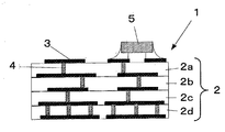
以下、本発明の多層配線基板について、図面に基づいて説明する。本発明の多層配線基板1によれば、絶縁基板2は、複数のガラスセラミック絶縁層2a〜2dを積層してなる積層体から構成され、その絶縁層間および絶縁基板表面には、厚みが10〜15μm程度の高純度金属箔からなる多孔質の配線回路層3が被着形成されている。さらに、各ガラスセラミック絶縁層2a〜2dには、厚み方向を貫くように形成された直径が80〜200μmのビアホ−ル導体4が形成され、これにより、所定回路を達成するための回路網が形成される。
【0014】
絶縁基板2は、ガラス成分が20〜80重量%、フィラー成分が20〜80重量%の割合で含有することが望ましい。
【0015】
なお、ガラスセラミックスを構成する前記ガラスとしては、少なくともSiO2を含み、Al2O3、B2O3、ZnO、PbO、アルカリ土類金属酸化物、アルカリ金属酸化物のうち少なくとも1種以上を含有し、焼成処理することによっても非晶質であるもの、また焼成処理によってコージェライト、ムライト、アノーサイト、セルジアン、スピネル、ガーナイト、ウィレマイト、ドロマイト、ペタライトやその置換誘導体の結晶を少なくとも1種を析出する結晶化ガラスが用いられる。
【0016】
また無機質フィラーとしては、クォーツ、クリストバライト、等のSiO2、Al2O3、ZrO2、ムライト、フォルステライト、エンスタタイト等が知られている。
【0017】
本発明によれば、配線回路層3は、99.5重量%以上の高純度な金属導体からなるもので、Cu、Ag、Al、Au、Ni、Pt、Pdから選ばれる少なくとも1種以上の金属箔からなることが望ましい。また、ビアホール導体4には、上記の配線回路層3と同様の導体成分が充填されていることが望ましい。
【0018】
本発明によれば、配線回路層3は、金属箔に孔が形成された高純度金属導体からなることが重要である。このような孔が形成された金属箔を用いることによって、絶縁基板との同時焼成時の熱収縮挙動の違いによる熱応力を多孔質体からなる配線回路層が吸収することによって絶縁基板の割れやクラックの発生を抑制することができる。但し、配線回路層の孔が多すぎると、配線回路層のシート抵抗が高くなる虞があるために、具体的には、配線回路層3の孔は平均径が10μm以下であり、その存在割合は面積比率で60%以下、特に40%以下、さらには20%以下であることが望ましい。
【0019】
また、多層配線基板の表面の配線回路層は、ICチップなどの各種電子部品5を搭載するためのパッドとして、シールド用導体膜として、さらには、外部回路と接続する端子電極として用いられ、各種電子部品5が配線回路層3に半田や導電性接着剤などを介して接合される。尚、図示していないが、必要に応じて、配線基板の表面には、さらに珪化タンタル、珪化モリブデンなどの厚膜抵抗体膜や配線保護膜などを形成しても構わない。
【0020】
次に、本発明の多層配線基板を作製する方法について説明する。まず、上述したような非晶質ガラス、又は結晶化ガラスと前記の無機質フィラー成分を混合してガラスセラミック組成物を調製し、その混合物に有機バインダー等を加えた後、ドクターブレード法、圧延法、プレス法等によりシート状に成形してグリーンシートを作製する。
【0021】
次に、このグリーンシートに、適宜、レーザーやマイクロドリル、パンチングなどにより、直径80〜200μmの貫通孔を形成し、その内部に導電性ペーストを充填する。
【0022】
導電性ペースト中には、Cu又はAgを主成分とする金属粉末以外に、アクリル樹脂などからなる有機バインダーとトルエン、イソプロピルアルコール、アセトンなどの有機溶剤とを均質混合して形成される。有機バインダは、金属成分100重量部に対して、0.5〜5.0重量部、有機溶剤は、固形成分及び有機バインダ100重量部に対して、5〜100重量部の割合で混合されることが望ましい。なお、この導電性ペースト中には若干のガラス成分等を添加してもよい。
【0023】
次に、このグリーンシートの表面に金属箔などの高純度金属導体からなる配線回路層を形成する。このような配線回路層の形成方法としては、(1)グリーンシートの表面に多孔質金属箔を接着した後、レジスト塗布、エッチング、レジスト除去の工程を経て回路パターンを形成する、(2)所定の転写フィルムに多孔質金属箔を接着した後、上記と同様にして回路パターンを形成した後、この回路パターンをグリーンシート表面に転写形成する、等の方法によって形成することができる。
【0024】
そこで、転写法による配線回路層の形成方法についてより具体的に説明する。まず、高分子材料等からなる転写フィルム上に、この多孔質な金属導体の表面に鏡像のレジストを回路パターン状に塗布した後、エッチング処理およびレジスト除去を行って鏡像の配線回路層を形成する。
【0025】
鏡像の配線回路層を形成した転写フィルムを前記ビアホール導体が形成されたグリーンシートの表面に位置合わせして積層圧着した後、転写シートを剥がすことにより、ビアホール導体と接続した配線回路層を具備する一単位のグリーンシートを形成することができる。その後、同様にして得られた複数のグリーンシートを積層圧着して積層体を形成する。
【0026】
次に、この積層体を400〜750℃の大気中または窒素雰囲気中で加熱処理してグリーンシート内やビアホール導電性ペースト中の有機成分を分解除去した後、800〜1000℃の大気または窒素雰囲気中で同時焼成することができる。この際、配線回路基板を多孔質体によって形成しているため、グリーンシートと同時焼成をおこなっても、多孔質体中の孔が、グリーンシートの焼成収縮に合わせてx−y軸方向に収縮するために、両者の焼結挙動の相違による熱応力の発生を抑制することができる結果、絶縁基板の反り、うねり等の発生を抑え、配線回路層およびビアホール導体を具備する多層配線基板を安定に作製することができる。
【0027】
なお、配線回路層やビアホール導体中の導体成分として銅を用いた場合には、焼成雰囲気は窒素雰囲気、Ag導体を用いた場合には大気中で焼成される。
【0028】
なお、本発明の製造方法で用いる金属箔に孔が形成された高純度金属導体は、金属箔を例えば樹脂フィルムに接着した後に、レーザーを用いて孔を形成するか、あるいは、あらかじめ孔が形成された金属箔を用いることもできる。孔が形成された金属箔は、例えば、緻密質な金属箔の表面にレジストを塗布した時、エッチング処理して孔を形成してもよい。
【0029】
金属箔に形成される孔は、平均径が30μm以下、特に20μm以下であり、その存在割合は面積比率で20〜70%、特に30〜50%であることが望ましい。これは平均径が大きすぎると微細配線化が難しく、面積比率が20%よりも小さいと、グリーンシートとの焼結挙動を十分に一致させることが難しく、70%よりも大きいと、焼成後の配線回路層のシート抵抗が高くなってしまう虞があるためである。
【0030】
【実施例】
実施例1
先ず、ホウケイ酸ガラスを70重量%、SiO2を30重量%の割合で秤量し、それに、バインダーとしてアクリル樹脂、可塑剤としてDBP(ジブチルフタレート)、溶媒としてトルエンとイソプロピルアルコールを加えて調製したスラリーを用いて、ドクターブレード法により厚さ500μmのグリーンシートを作製した。
【0031】
次に、平均粒径が5μmのCu粉末と、それに有機バインダーとしてアクリル樹脂を、溶媒としてジブチルフタレートを添加混練し、ビアホール導体用ペーストを作製した。なお、前記ビアホール導体用ペースト中の有機バインダーは、Cu単体100重量部に対して2.0重量部加え、さらに溶剤をCu単体、有機バインダー100重量部に対して75重量部加えた。
【0032】
次に、上記のグリーンシートの所定個所にビアホールを形成し、そのビアホール内に先のCuペーストを充填した。
【0033】
次にPETからなる転写フィルムに純度99.5重量%以上の厚み15μmのCu箔を接着し、レーザーで5〜10μmの孔を形成した。孔は単位面積あたりで20〜30%とした。
【0034】
次に、配線パターンの鏡像のレジストを塗布後、エッチング処理、レジスト除去を行い、鏡像の配線回路層を形成した。配線幅は0.05mmとしたが、エッチングによる形成のため、従来のスクリーン印刷法と比較して、非常に微細な配線回路層を形成することができた。
【0035】
そして、ビアホールが形成されたグリーンシートにビアホールの位置あわせを行いながら転写フィルムを積層し、60℃、150kgf/cm2で熱圧着した。転写フィルムを剥がすことにより、ビアホール導体を接続した配線回路層を具備する一単位のグリーンシートを形成した。
【0036】
同様にして作製した5枚のグリーンシートと共に60℃、150kgf/cm2で加圧積層して積層体を作製した。
【0037】
次いで、この未焼成状態の積層体を、有機バインダー等の有機成分を分解除去するために、窒素雰囲気中、700℃で焼成し、次に窒素雰囲気中900℃で焼成を行い、配線基板を作製した。
【0038】
得られた配線基板の表面を走査型電子顕微鏡(SEM)を用い、クラックの有無を確認した。クラック無を良品とした。
【0039】
また、得られた配線基板を用いて配線回路層の比抵抗の評価を行った。評価については、幅0.05mm、長さ20mmの銅配線層を予め形成し、配線抵抗をテスターを用いて測定し、銅配線層の断面を走査型電子顕微鏡(SEM)、銅配線の長さを40倍の顕微鏡を用いて測定し、得られた面積、長さから抵抗率を算出した。なお、良否の判断は、抵抗率が2.5μΩ・cm以下を良品とした。また、得られた配線基板の対角線上の反りを、表面粗さ計を用いて測定した。Rmaxで50μm以下を良品とした。
【0040】
実施例2、3、4
配線回路層を形成する高純度金属導体として、純度が99.5重量%以上のAg、Ag−Pd、Ag−Ptの各金属箔を用い、実施例1と同様の仕様で多層配線基板を作製した。焼成についてはいづれも大気中、900℃で焼成を行った。評価結果については表1に示す。
【0041】
比較例1
実施例1と同様の仕様とし、配線回路層の形成方法を金属箔の転写に代えて従来のCuペーストによるスクリーン印刷法で行った。評価結果については表1に示す。
【0042】
比較例2
配線回路層を多孔質ではない緻密質のCu箔で形成した以外は、実施例1と同様の仕様とし、評価を行った。評価結果については表1に示す。
【0043】
【表1】
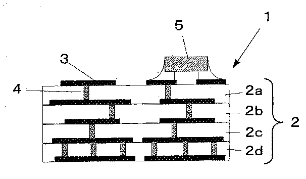
表1より、スクリーン印刷法で配線回路層を形成した試料No.5は、断線が発生しており、印刷法による配線幅0.05mmの微細配線が形成できなかった。多孔質でないCu箔で配線回路層を形成した試料No.6は絶縁基板の表面にクラックが発生し、また絶縁基板の反りがRmaxで50μmを越えており、実用的ではない。
【0045】
これら比較例に対して、本発明の多層配線基板によれば、x−y軸方向に収縮可能な配線回路層を具備することで、焼成後のクラックの発生を減少させることができ、微細配線化、低抵抗化に対しても満足できるものであった。
【0046】
【発明の効果】
以上詳述したとおり、本発明によれば、配線回路層として孔が形成された金属箔などの高純度の金属導体を用いることによって、微細配線化を可能とし、配線回路層の低抵抗化を満足しつつ、簡単な方法で、且つ反り、うねりの小さい多層配線基板を作製することができる。
【図面の簡単な説明】
【図1】本発明の多層配線基板を説明するための概略図である。
【符号の説明】
1 多層配線基板
2 絶縁基板
3 配線回路層
4 ビアホール導体
5 電子部品[0001]
BACKGROUND OF THE INVENTION
The present invention relates to a multilayer wiring board suitable for a package for housing a semiconductor element and a method for manufacturing the same.
[0002]
[Prior art]
Conventionally, a multilayer ceramic wiring board capable of relatively high density wiring has been widely used as a wiring board, for example, a multilayer wiring board used for a package for housing a semiconductor element. This multilayer ceramic wiring board is composed of an insulating substrate such as alumina or glass ceramic and a wiring conductor made of metal such as W, Mo, Cu, or Ag formed on the surface thereof. A cavity is formed in the part, a semiconductor element is accommodated in the cavity, and the cavity is hermetically sealed by a lid.
[0003]
In recent years, in a wiring board applied to a package for housing a semiconductor element in which semiconductor elements such as IC and LSI, which have been highly integrated, are mounted, and a hybrid integrated circuit device in which various electronic components are mounted, the density and There is a demand for resistance and a reduction in size and weight, and a glass ceramic wiring board that can obtain a lower dielectric constant than an alumina-based ceramic material and can reduce the resistance of a wiring layer has attracted more attention.
[0004]
However, in such a glass ceramic wiring board, as a method of forming a wiring circuit layer, a metallized paste mainly composed of a conductor made of a metal such as Cu or Ag is printed on an insulating substrate by a screen printing method or the like. A method of firing simultaneously with the insulating substrate is employed. However, when such a method is used, it is difficult to form a wiring width of 100 μm or less by printing, which is a cause of hindering the achievement of further higher density and reduction in size and weight that will be required in the future.
[0005]
As a technique for solving this problem, a technique of forming a wiring circuit layer in a glass ceramic green sheet by etching a metal foil is known (Japanese Patent Laid-Open No. 63-14493). In addition, as a method of manufacturing a wiring board using a metal foil as a wiring circuit layer, both sides of a laminated body of glass ceramic green sheets on which a wiring circuit layer made of a metal foil is formed are not sintered at the firing temperature of the wiring board. It has also been proposed to simultaneously fire the metal foil and the glass ceramic insulating substrate while laminating the inorganic sheets and then simultaneously firing to suppress shrinkage in the xy-axis direction of the wiring board (Japanese Patent Laid-Open No. 7-86743). issue).
[0006]
[Problems to be solved by the invention]
In the case of simultaneous firing of the glass ceramic molded body and the wiring circuit layer made of Cu paste, thermal stress is absorbed in the sintering process of both, but when using the wiring circuit layer made of metal foil, the wiring circuit Since the layer itself is made of a high-rigidity dense body, most of the thermal stress is applied to the glass-ceramic insulating substrate side. Therefore, in the cooling process after simultaneous firing, the wiring circuit layer forming surface of the glass-ceramic insulating substrate Cracks occurred in some cases, and in some cases, the insulating substrate was destroyed.
[0007]
In addition, in the method of laminating and firing the inorganic sheet that does not sinter at the firing temperature during firing, it is possible to suppress the generation of thermal stress on the insulating substrate, but because a step of removing the inorganic sheet after firing is necessary, There have also been problems such as an increase in cost, a roughened substrate surface after removal, and a tendency for cracks to occur in the glass ceramic insulating substrate during the removal process.
[0008]
Therefore, the object of the present invention is to achieve fine wiring and low resistance in a glass ceramic wiring board, and a metal foil and a glass ceramic molded body can be stably produced by simultaneous firing, such as warping. An object of the present invention is to provide a small multilayer wiring board and a manufacturing method thereof.
[0009]
[Means for Solving the Problems]
As a result of intensive studies on the problems as described above, the inventors of the present invention have a high purity in which a hole is formed in a metal foil having a metal component content of 99.5% by weight or more as a wiring circuit layer in a glass ceramic wiring board. By using a porous body made of a metal conductor, the rigidity of the high-purity metal conductor itself is relaxed and the shrinkage in the xy-axis direction is possible. It was.
[0010]
That is, the multilayer wiring board of the present invention is a wiring board comprising an insulating substrate made of glass ceramics and a wiring circuit layer formed on the surface and / or inside of the insulating substrate, and at least the inside of the insulating substrate. And an internal wiring circuit layer made of a porous high-purity metal conductor in which holes are formed in a metal foil having a metal component content of 99.5% by weight or more, and the wiring circuit layer has an xy-axis direction. be contracted by firing accompanied to be one, wherein, said metal foil, Cu, Ag, Al, Au , Ni, Pt, be composed of at least one element selected from Pd desirable And a via hole conductor filled with a conductive paste containing metal powder inside the insulating substrate, and at least one end of the via hole conductor is connected to the internal wiring circuit layer. Those characterized by comprising. Furthermore, it is preferable that the average diameter of the hole provided in the said metal foil is 30 micrometers or less, and an area ratio is 20 to 70%.
[0011]
The multilayer wiring board manufacturing method of the present invention includes (a) a step of producing a green sheet made of a glass ceramic composition, and (b) a metal component content of 99.5 on the green sheet surface. A step of forming a porous wiring circuit layer made of a high-purity metal conductor in which holes are formed in a metal foil of wt% or more, and a green sheet produced through the steps (c), (a) and (b), (D) heating the laminate to a temperature not higher than the melting point of the high-purity metal conductor, and shrinking the wiring circuit layer in the xy-axis direction. And a step of sintering the sheet.
[0012]
The high-purity metal conductor is preferably made of at least one porous metal foil selected from Cu, Ag, Al, Au, Ni, Pt, and Pd, and in the step (b), the wiring Before the circuit layer is formed, a step of forming a via hole in the green sheet and filling the via hole with a conductive paste can be added. Furthermore, it is desirable that holes with an average diameter of 2 to 30 μm are formed uniformly in the metal foil, and the holes are present in an area ratio of 20 to 70%.
[0013]
DETAILED DESCRIPTION OF THE INVENTION
Hereinafter, a multilayer wiring board of the present invention will be described with reference to the drawings. According to the
[0014]
The
[0015]
The glass constituting the glass ceramic contains at least SiO 2 and contains at least one of Al 2 O 3 , B 2 O 3 , ZnO, PbO, alkaline earth metal oxide, and alkali metal oxide. Containing and at least one amorphous crystal of cordierite, mullite, anorthite, serzian, spinel, garnite, willemite, dolomite, petalite and substituted derivatives thereof by firing treatment Precipitated crystallized glass is used.
[0016]
As inorganic fillers, quartz, cristobalite, etc., SiO 2 , Al 2 O 3 , ZrO 2 , mullite, forsterite, enstatite and the like are known.
[0017]
According to the present invention, the
[0018]
According to the present invention, it is important that the
[0019]
The wiring circuit layer on the surface of the multilayer wiring board is used as a pad for mounting various
[0020]
Next, a method for producing the multilayer wiring board of the present invention will be described. First, an amorphous glass as described above or crystallized glass and the above inorganic filler component are mixed to prepare a glass ceramic composition, and after adding an organic binder or the like to the mixture, a doctor blade method, a rolling method Then, a green sheet is produced by forming into a sheet shape by a pressing method or the like.
[0021]
Next, a through hole having a diameter of 80 to 200 μm is appropriately formed in the green sheet by a laser, a micro drill, punching, or the like, and the inside thereof is filled with a conductive paste.
[0022]
In the conductive paste, an organic binder made of an acrylic resin or the like and an organic solvent such as toluene, isopropyl alcohol, or acetone are homogeneously mixed in addition to the metal powder mainly containing Cu or Ag. The organic binder is mixed at 0.5 to 5.0 parts by weight with respect to 100 parts by weight of the metal component, and the organic solvent is mixed at a ratio of 5 to 100 parts by weight with respect to 100 parts by weight of the solid component and the organic binder. It is desirable. In addition, you may add some glass components etc. in this electrically conductive paste.
[0023]
Next, a wiring circuit layer made of a high-purity metal conductor such as a metal foil is formed on the surface of the green sheet. As a method for forming such a wiring circuit layer, (1) a porous metal foil is bonded to the surface of a green sheet, and then a circuit pattern is formed through steps of resist coating, etching, and resist removal. After the porous metal foil is bonded to the transfer film, a circuit pattern is formed in the same manner as described above, and then the circuit pattern is transferred and formed on the surface of the green sheet.
[0024]
Therefore, a method for forming a wiring circuit layer by a transfer method will be described more specifically. First, on a transfer film made of a polymer material or the like, a mirror image resist is applied to the surface of the porous metal conductor in a circuit pattern, and then etching treatment and resist removal are performed to form a mirror image wiring circuit layer. .
[0025]
A transfer film on which a mirror circuit wiring circuit layer is formed is aligned with the surface of the green sheet on which the via-hole conductor is formed and laminated and pressure-bonded, and then the transfer sheet is peeled off to provide a wiring circuit layer connected to the via-hole conductor. One unit of green sheet can be formed. Thereafter, a plurality of green sheets obtained in the same manner are laminated and pressure-bonded to form a laminate.
[0026]
Next, this laminate is heat-treated in the air at 400 to 750 ° C. or in a nitrogen atmosphere to decompose and remove the organic components in the green sheet and the via-hole conductive paste, and then in the air or nitrogen atmosphere at 800 to 1000 ° C. Can be co-fired in. At this time, since the printed circuit board is formed of a porous body, even if simultaneous firing with the green sheet is performed, the pores in the porous body shrink in the xy-axis direction in accordance with the firing shrinkage of the green sheet. As a result, it is possible to suppress the generation of thermal stress due to the difference in sintering behavior between the two, thereby suppressing the occurrence of warping and undulation of the insulating substrate and stabilizing the multilayer wiring substrate having the wiring circuit layer and the via-hole conductor. Can be produced.
[0027]
When copper is used as the conductor component in the wiring circuit layer or via-hole conductor, the firing atmosphere is fired in a nitrogen atmosphere, and when an Ag conductor is used, firing is performed in the air.
[0028]
In addition, the high-purity metal conductor in which holes are formed in the metal foil used in the manufacturing method of the present invention is formed by using a laser after bonding the metal foil to, for example, a resin film, or by forming holes in advance. It is also possible to use a metal foil. Metal foil holes are formed, for example, when applying a resist on the surface of the dense metal foil may be an etching process to the hole.
[0029]
The holes formed in the metal foil have an average diameter of 30 μm or less, particularly 20 μm or less, and the presence ratio is preferably 20 to 70%, particularly 30 to 50% in terms of area ratio. If the average diameter is too large, it is difficult to make fine wiring, and if the area ratio is less than 20%, it is difficult to make the sintering behavior sufficiently coincide with the green sheet. This is because the sheet resistance of the wiring circuit layer may be increased.
[0030]
【Example】
Example 1
First, a slurry prepared by weighing 70% by weight of borosilicate glass and 30% by weight of SiO 2 , adding acrylic resin as a binder, DBP (dibutyl phthalate) as a plasticizer, and toluene and isopropyl alcohol as solvents. Was used to prepare a green sheet having a thickness of 500 μm by the doctor blade method.
[0031]
Next, Cu powder having an average particle diameter of 5 μm, an acrylic resin as an organic binder, and dibutyl phthalate as a solvent were added and kneaded to prepare a via-hole conductor paste. In addition, the organic binder in the said via-hole conductor paste added 2.0 weight part with respect to 100 weight part of Cu simple substance, and also added 75 weight part of solvent with respect to Cu simple substance and 100 weight part of organic binder.
[0032]
Next, a via hole was formed in a predetermined portion of the green sheet, and the previous Cu paste was filled in the via hole.
[0033]
Next, a 15 μm thick Cu foil having a purity of 99.5% by weight or more was bonded to a transfer film made of PET, and 5 to 10 μm holes were formed with a laser. The pores were 20-30% per unit area.
[0034]
Next, after applying a mirror image resist of the wiring pattern, etching treatment and resist removal were performed to form a mirror image wiring circuit layer. Although the wiring width was 0.05 mm, because of the formation by etching, a very fine wiring circuit layer could be formed as compared with the conventional screen printing method.
[0035]
Then, a transfer film was laminated on the green sheet on which the via hole was formed while aligning the via hole, and thermocompression bonded at 60 ° C. and 150 kgf / cm 2 . By peeling off the transfer film, one unit of green sheet having a wiring circuit layer to which via-hole conductors were connected was formed.
[0036]
A laminate was produced by pressure laminating together with five green sheets produced in the same manner at 60 ° C. and 150 kgf / cm 2 .
[0037]
Next, in order to decompose and remove organic components such as an organic binder, this unfired laminate is fired at 700 ° C. in a nitrogen atmosphere, and then fired at 900 ° C. in a nitrogen atmosphere to produce a wiring board. did.
[0038]
The surface of the obtained wiring board was checked for the presence of cracks using a scanning electron microscope (SEM). No cracks were considered good products.
[0039]
Moreover, the specific resistance of the wiring circuit layer was evaluated using the obtained wiring board. For the evaluation, a copper wiring layer having a width of 0.05 mm and a length of 20 mm was formed in advance, the wiring resistance was measured using a tester, the cross section of the copper wiring layer was measured with a scanning electron microscope (SEM), and the length of the copper wiring. Was measured using a 40 × microscope, and the resistivity was calculated from the obtained area and length. In addition, the judgment of pass / fail was made a non-defective product having a resistivity of 2.5 μΩ · cm or less. Moreover, the warpage on the diagonal of the obtained wiring board was measured using a surface roughness meter. Rmax of 50 μm or less was regarded as a good product.
[0040]
Examples 2, 3, 4
As a high-purity metal conductor for forming a wiring circuit layer, a multilayer wiring board is produced with the same specifications as in Example 1 using each metal foil of Ag, Ag-Pd, Ag-Pt having a purity of 99.5% by weight or more. did. As for firing, firing was performed at 900 ° C. in the air. The evaluation results are shown in Table 1.
[0041]
Comparative Example 1
The specification was the same as in Example 1, and the wiring circuit layer was formed by a conventional screen printing method using a Cu paste instead of transferring the metal foil. The evaluation results are shown in Table 1.
[0042]
Comparative Example 2
The evaluation was performed with the same specifications as in Example 1 except that the wiring circuit layer was formed of a dense Cu foil that was not porous. The evaluation results are shown in Table 1.
[0043]
[Table 1]
From Table 1, sample No. 1 in which the wiring circuit layer was formed by the screen printing method was used. No. 5 was disconnected, and fine wiring with a wiring width of 0.05 mm by the printing method could not be formed. Sample No. in which a wiring circuit layer was formed with a non-porous Cu foil. No. 6 is not practical because cracks are generated on the surface of the insulating substrate and the warpage of the insulating substrate exceeds 50 μm in Rmax.
[0045]
In contrast to these comparative examples, according to the multilayer wiring board of the present invention, it is possible to reduce the occurrence of cracks after firing by providing a wiring circuit layer that can shrink in the xy axis direction. Satisfying the reduction in resistance and resistance.
[0046]
【The invention's effect】
As described above in detail, according to the present invention, by using a high-purity metal conductor such as a metal foil having a hole as a wiring circuit layer, it is possible to make fine wiring and reduce the resistance of the wiring circuit layer. While satisfying, it is possible to manufacture a multilayer wiring board with a simple method and with small warpage and undulation.
[Brief description of the drawings]
FIG. 1 is a schematic view for explaining a multilayer wiring board of the present invention.
[Explanation of symbols]
DESCRIPTION OF
Claims (8)
Priority Applications (1)
| Application Number | Priority Date | Filing Date | Title |
|---|---|---|---|
| JP33988399A JP4071908B2 (en) | 1999-11-30 | 1999-11-30 | Multilayer wiring board and manufacturing method thereof |
Applications Claiming Priority (1)
| Application Number | Priority Date | Filing Date | Title |
|---|---|---|---|
| JP33988399A JP4071908B2 (en) | 1999-11-30 | 1999-11-30 | Multilayer wiring board and manufacturing method thereof |
Publications (2)
| Publication Number | Publication Date |
|---|---|
| JP2001156411A JP2001156411A (en) | 2001-06-08 |
| JP4071908B2 true JP4071908B2 (en) | 2008-04-02 |
Family
ID=18331729
Family Applications (1)
| Application Number | Title | Priority Date | Filing Date |
|---|---|---|---|
| JP33988399A Expired - Fee Related JP4071908B2 (en) | 1999-11-30 | 1999-11-30 | Multilayer wiring board and manufacturing method thereof |
Country Status (1)
| Country | Link |
|---|---|
| JP (1) | JP4071908B2 (en) |
Families Citing this family (3)
| Publication number | Priority date | Publication date | Assignee | Title |
|---|---|---|---|---|
| JP5072289B2 (en) * | 2006-08-30 | 2012-11-14 | 京セラ株式会社 | Airtight terminal |
| US8568855B2 (en) * | 2011-06-08 | 2013-10-29 | Siemens Energy, Inc. | Insulation materials having apertures formed therein |
| JP6819599B2 (en) | 2015-09-25 | 2021-01-27 | 大日本印刷株式会社 | Mounting components, wiring boards, electronic devices, and their manufacturing methods |
Family Cites Families (3)
| Publication number | Priority date | Publication date | Assignee | Title |
|---|---|---|---|---|
| JPH05174613A (en) * | 1991-12-26 | 1993-07-13 | Matsushita Electric Ind Co Ltd | Electrode for wiring ceramic circuit substrate and electrode paste |
| JPH10242644A (en) * | 1997-02-26 | 1998-09-11 | Hitachi Ltd | GREEN SHEET WITH CONDUCTOR CIRCUIT, PROCESS FOR PRODUCING THE SAME, AND MULTILAYER WIRING CERAMIC SUBSTRATE USING THE SAME |
| JPH11103141A (en) * | 1997-09-26 | 1999-04-13 | Kyocera Corp | Wiring board |
-
1999
- 1999-11-30 JP JP33988399A patent/JP4071908B2/en not_active Expired - Fee Related
Also Published As
| Publication number | Publication date |
|---|---|
| JP2001156411A (en) | 2001-06-08 |
Similar Documents
| Publication | Publication Date | Title |
|---|---|---|
| JP3652196B2 (en) | Manufacturing method of ceramic wiring board | |
| JP4454105B2 (en) | Manufacturing method of multilayer wiring board | |
| JP4610114B2 (en) | Manufacturing method of ceramic wiring board | |
| JP4535576B2 (en) | Manufacturing method of multilayer wiring board | |
| JP4071908B2 (en) | Multilayer wiring board and manufacturing method thereof | |
| JP3774336B2 (en) | High frequency wiring board and manufacturing method thereof | |
| JP4535098B2 (en) | Manufacturing method of multilayer ceramic electronic component | |
| JP4029163B2 (en) | Multilayer ceramic electronic component and manufacturing method thereof | |
| JP2004087989A (en) | Multilayer wiring board | |
| JP4028810B2 (en) | Manufacturing method of multilayer wiring board | |
| JP3886791B2 (en) | Manufacturing method of multilayer wiring board | |
| JP2002050865A (en) | Glass ceramic wiring board and method of manufacturing the same | |
| JP2004063811A (en) | Wiring board and method of manufacturing the same | |
| JP4587562B2 (en) | Manufacturing method of multilayer wiring board | |
| JP4535801B2 (en) | Ceramic wiring board | |
| JP2001015930A (en) | Multilayer wiring board and method of manufacturing the same | |
| JP3426920B2 (en) | Wiring board | |
| JP3188086B2 (en) | Ceramic wiring board, its manufacturing method and its mounting structure | |
| JP2004235347A (en) | Insulating ceramics and multilayer ceramic substrate using the same | |
| JP2004119547A (en) | Ceramic wiring board and method of manufacturing the same | |
| JP2001102756A (en) | Multilayer wiring board and method of manufacturing the same | |
| JP4157352B2 (en) | Wiring board | |
| JP2002359465A (en) | Method for manufacturing multilayer wiring board | |
| JP2001068852A (en) | Multilayer wiring board and method of manufacturing the same | |
| JP2003078245A (en) | Method for manufacturing multilayer wiring board |
Legal Events
| Date | Code | Title | Description |
|---|---|---|---|
| A131 | Notification of reasons for refusal |
Free format text: JAPANESE INTERMEDIATE CODE: A131 Effective date: 20040622 |
|
| A521 | Written amendment |
Free format text: JAPANESE INTERMEDIATE CODE: A523 Effective date: 20040823 |
|
| A02 | Decision of refusal |
Effective date: 20050208 Free format text: JAPANESE INTERMEDIATE CODE: A02 |
|
| A521 | Written amendment |
Free format text: JAPANESE INTERMEDIATE CODE: A523 Effective date: 20050408 |
|
| A911 | Transfer of reconsideration by examiner before appeal (zenchi) |
Effective date: 20050413 Free format text: JAPANESE INTERMEDIATE CODE: A911 |
|
| A912 | Removal of reconsideration by examiner before appeal (zenchi) |
Free format text: JAPANESE INTERMEDIATE CODE: A912 Effective date: 20050520 |
|
| A61 | First payment of annual fees (during grant procedure) |
Effective date: 20080118 Free format text: JAPANESE INTERMEDIATE CODE: A61 |
|
| R150 | Certificate of patent (=grant) or registration of utility model |
Free format text: JAPANESE INTERMEDIATE CODE: R150 |
|
| FPAY | Renewal fee payment (prs date is renewal date of database) |
Year of fee payment: 3 Free format text: PAYMENT UNTIL: 20110125 |
|
| LAPS | Cancellation because of no payment of annual fees |