JP4004705B2 - Imaging device and imaging device assembling method - Google Patents
Imaging device and imaging device assembling method Download PDFInfo
- Publication number
- JP4004705B2 JP4004705B2 JP2000053400A JP2000053400A JP4004705B2 JP 4004705 B2 JP4004705 B2 JP 4004705B2 JP 2000053400 A JP2000053400 A JP 2000053400A JP 2000053400 A JP2000053400 A JP 2000053400A JP 4004705 B2 JP4004705 B2 JP 4004705B2
- Authority
- JP
- Japan
- Prior art keywords
- circuit board
- printed circuit
- lens
- adhesive
- imaging device
- Prior art date
- Legal status (The legal status is an assumption and is not a legal conclusion. Google has not performed a legal analysis and makes no representation as to the accuracy of the status listed.)
- Expired - Lifetime
Links
- 238000003384 imaging method Methods 0.000 title claims description 53
- 238000000034 method Methods 0.000 title description 15
- 239000000853 adhesive Substances 0.000 claims description 58
- 230000001070 adhesive effect Effects 0.000 claims description 58
- 239000004065 semiconductor Substances 0.000 claims description 37
- 230000002093 peripheral effect Effects 0.000 claims description 16
- 230000003287 optical effect Effects 0.000 description 27
- 238000004519 manufacturing process Methods 0.000 description 9
- 230000035945 sensitivity Effects 0.000 description 7
- 229910000679 solder Inorganic materials 0.000 description 7
- 238000005476 soldering Methods 0.000 description 4
- 238000010586 diagram Methods 0.000 description 3
- 230000000694 effects Effects 0.000 description 3
- 230000003321 amplification Effects 0.000 description 2
- 239000003990 capacitor Substances 0.000 description 2
- 239000000428 dust Substances 0.000 description 2
- 230000001788 irregular Effects 0.000 description 2
- 238000003199 nucleic acid amplification method Methods 0.000 description 2
- 230000005855 radiation Effects 0.000 description 2
- 239000007787 solid Substances 0.000 description 2
- 239000000758 substrate Substances 0.000 description 2
- 230000002411 adverse Effects 0.000 description 1
- 230000000712 assembly Effects 0.000 description 1
- 238000000429 assembly Methods 0.000 description 1
- 239000003795 chemical substances by application Substances 0.000 description 1
- 230000003247 decreasing effect Effects 0.000 description 1
- 230000000593 degrading effect Effects 0.000 description 1
- 239000011521 glass Substances 0.000 description 1
- 238000003780 insertion Methods 0.000 description 1
- 230000037431 insertion Effects 0.000 description 1
- WABPQHHGFIMREM-UHFFFAOYSA-N lead(0) Chemical compound [Pb] WABPQHHGFIMREM-UHFFFAOYSA-N 0.000 description 1
- 239000007769 metal material Substances 0.000 description 1
- 238000000465 moulding Methods 0.000 description 1
- 239000003973 paint Substances 0.000 description 1
- 239000011347 resin Substances 0.000 description 1
- 229920005989 resin Polymers 0.000 description 1
Images


Classifications
-
- H—ELECTRICITY
- H04—ELECTRIC COMMUNICATION TECHNIQUE
- H04N—PICTORIAL COMMUNICATION, e.g. TELEVISION
- H04N23/00—Cameras or camera modules comprising electronic image sensors; Control thereof
-
- H—ELECTRICITY
- H01—ELECTRIC ELEMENTS
- H01L—SEMICONDUCTOR DEVICES NOT COVERED BY CLASS H10
- H01L27/00—Devices consisting of a plurality of semiconductor or other solid-state components formed in or on a common substrate
- H01L27/14—Devices consisting of a plurality of semiconductor or other solid-state components formed in or on a common substrate including semiconductor components sensitive to infrared radiation, light, electromagnetic radiation of shorter wavelength or corpuscular radiation and specially adapted either for the conversion of the energy of such radiation into electrical energy or for the control of electrical energy by such radiation
- H01L27/144—Devices controlled by radiation
- H01L27/146—Imager structures
- H01L27/14601—Structural or functional details thereof
- H01L27/14618—Containers
-
- H—ELECTRICITY
- H01—ELECTRIC ELEMENTS
- H01L—SEMICONDUCTOR DEVICES NOT COVERED BY CLASS H10
- H01L27/00—Devices consisting of a plurality of semiconductor or other solid-state components formed in or on a common substrate
- H01L27/14—Devices consisting of a plurality of semiconductor or other solid-state components formed in or on a common substrate including semiconductor components sensitive to infrared radiation, light, electromagnetic radiation of shorter wavelength or corpuscular radiation and specially adapted either for the conversion of the energy of such radiation into electrical energy or for the control of electrical energy by such radiation
- H01L27/144—Devices controlled by radiation
- H01L27/146—Imager structures
- H01L27/14601—Structural or functional details thereof
- H01L27/14625—Optical elements or arrangements associated with the device
-
- H—ELECTRICITY
- H01—ELECTRIC ELEMENTS
- H01L—SEMICONDUCTOR DEVICES NOT COVERED BY CLASS H10
- H01L27/00—Devices consisting of a plurality of semiconductor or other solid-state components formed in or on a common substrate
- H01L27/14—Devices consisting of a plurality of semiconductor or other solid-state components formed in or on a common substrate including semiconductor components sensitive to infrared radiation, light, electromagnetic radiation of shorter wavelength or corpuscular radiation and specially adapted either for the conversion of the energy of such radiation into electrical energy or for the control of electrical energy by such radiation
- H01L27/144—Devices controlled by radiation
- H01L27/146—Imager structures
- H01L27/14683—Processes or apparatus peculiar to the manufacture or treatment of these devices or parts thereof
- H01L27/14685—Process for coatings or optical elements
-
- H—ELECTRICITY
- H01—ELECTRIC ELEMENTS
- H01L—SEMICONDUCTOR DEVICES NOT COVERED BY CLASS H10
- H01L31/00—Semiconductor devices sensitive to infrared radiation, light, electromagnetic radiation of shorter wavelength or corpuscular radiation and specially adapted either for the conversion of the energy of such radiation into electrical energy or for the control of electrical energy by such radiation; Processes or apparatus specially adapted for the manufacture or treatment thereof or of parts thereof; Details thereof
- H01L31/02—Details
- H01L31/0203—Containers; Encapsulations, e.g. encapsulation of photodiodes
-
- H—ELECTRICITY
- H01—ELECTRIC ELEMENTS
- H01L—SEMICONDUCTOR DEVICES NOT COVERED BY CLASS H10
- H01L31/00—Semiconductor devices sensitive to infrared radiation, light, electromagnetic radiation of shorter wavelength or corpuscular radiation and specially adapted either for the conversion of the energy of such radiation into electrical energy or for the control of electrical energy by such radiation; Processes or apparatus specially adapted for the manufacture or treatment thereof or of parts thereof; Details thereof
- H01L31/02—Details
- H01L31/0232—Optical elements or arrangements associated with the device
- H01L31/02325—Optical elements or arrangements associated with the device the optical elements not being integrated nor being directly associated with the device
-
- H—ELECTRICITY
- H04—ELECTRIC COMMUNICATION TECHNIQUE
- H04N—PICTORIAL COMMUNICATION, e.g. TELEVISION
- H04N23/00—Cameras or camera modules comprising electronic image sensors; Control thereof
- H04N23/50—Constructional details
- H04N23/54—Mounting of pick-up tubes, electronic image sensors, deviation or focusing coils
-
- H—ELECTRICITY
- H04—ELECTRIC COMMUNICATION TECHNIQUE
- H04N—PICTORIAL COMMUNICATION, e.g. TELEVISION
- H04N23/00—Cameras or camera modules comprising electronic image sensors; Control thereof
- H04N23/50—Constructional details
- H04N23/55—Optical parts specially adapted for electronic image sensors; Mounting thereof
-
- H—ELECTRICITY
- H01—ELECTRIC ELEMENTS
- H01L—SEMICONDUCTOR DEVICES NOT COVERED BY CLASS H10
- H01L2924/00—Indexing scheme for arrangements or methods for connecting or disconnecting semiconductor or solid-state bodies as covered by H01L24/00
- H01L2924/0001—Technical content checked by a classifier
- H01L2924/0002—Not covered by any one of groups H01L24/00, H01L24/00 and H01L2224/00
Landscapes
- Engineering & Computer Science (AREA)
- Physics & Mathematics (AREA)
- Power Engineering (AREA)
- Microelectronics & Electronic Packaging (AREA)
- Electromagnetism (AREA)
- Condensed Matter Physics & Semiconductors (AREA)
- General Physics & Mathematics (AREA)
- Computer Hardware Design (AREA)
- Signal Processing (AREA)
- Multimedia (AREA)
- Transforming Light Signals Into Electric Signals (AREA)
- Studio Devices (AREA)
- Solid State Image Pick-Up Elements (AREA)
- Lens Barrels (AREA)
Description
【0001】
【発明の属する技術分野】
本発明は、監視カメラ、医療用カメラ、車載用カメラ等の半導体撮像素子を用いて小型化された撮像装置およびその組立方法に関する。
【0002】
【従来の技術】
従来、この種の撮像装置は、レンズが撮像した映像を電気信号に変換する半導体撮像素子の小型化、高性能化に伴い、カメラも小型化されて各方面で使用され、世の中の利便性を高めており、またカメラが小型になることで、映像の入力センサーとしての市場を広げている。
【0003】
従来の半導体撮像素子を用いた撮像装置は、レンズ、半導体撮像素子、LSI等の部品をそれぞれ筐体あるいは構造体に構成してそれらを組み合わせていた。また、プリント基板は平板状であり、その上に半導体撮像素子の駆動に必要な部品を実装する構造を有していた。
【0004】
【発明が解決しようとする課題】
しかしながら、このような従来のカメラの組立方式では、半導体撮像素子を小型化しても、各部品を接続して組み立てる構造では小型化に限界があり、組立に熟練が必要であったり、自動機械で組み立てられないという問題があった。
【0005】
本発明は、このような従来の問題を解決するものであり、一層の小型化と自動機械による組立を可能とした撮像装置およびその組立方法を提供するものである。
【0006】
【課題を解決するための手段】
本発明の撮像装置は、裏面に配線パターンを形成された矩形台状の脚部と前記脚部上に設けられた有底円筒形の胴部と前記脚部および前記胴部の境界に形成された開口部とを有する立体プリント基板と、前記脚部の裏面に前記開口部を塞ぐように装着された半導体撮像素子と、前記胴部の内部に保持されて前記半導体撮像素子に光を入射させるレンズとを備えたものである。この構成により、撮像装置に必要な総ての部品を立体プリント基板に集約して小型化することができることとなり、自動機械による組立が可能となる。
【0008】
また、本発明の撮像装置は、前記開口部の胴部側に前記開口部を塞ぐように装着された光学フィルタを備えたことを特徴とする。この構成により、撮像装置を構成するレンズ、光学フィルター、半導体撮像素子等のための専用の保持部品や接合組立等をなくして、立体プリント基板に総てを集約して小型化することができることとなる。
【0009】
また、本発明の撮像装置は、前記脚部に前記配線パターンを形成された段部を備え、前記段部にLSIとチップ部品とを片面または両面に接合したプリント基板を装着したことを特徴とする。この構成により、さらに多くの機能を撮像装置に付加することができることとなる。また、半導体撮像素子を駆動するLSIと周辺の部品の距離を短縮することができ、クロック信号の波形の歪および不要輻射を防止することができることとなる。
【0010】
また、本発明の撮像装置は、前記立体プリント基板の前記脚部裏面のうちの底面に形成された配線パターンには、他のプリント基板が直接的に電気接続されていることを特徴とする。この構成により、組み立てられた立体プリント基板を、携帯電話、パソコン、各種センサーのメイン基板に直接取り付けることができ、小型化の実現と、コネクター等を必要としないため軽量構造が実現できることとなる。
【0011】
また、本発明の撮像装置は、前記立体プリント基板の裏面に形成されている配線パターンが前記立体プリント基板の側面まで達するように形成されていることを特徴とする。この構成により、他のプリント基板のコネクターに立体プリント基板を差し込んで電気接合を行うことが可能となる。
【0012】
また、本発明の撮像装置は、脚部とこの脚部上に設けられた筒状の胴部とを有する立体プリント基板を備え、前記脚部の裏面に半導体撮像素子を装着し、前記胴部の内部に前記撮像素子に光を入射させるためのレンズを保持した撮像装置において、前記立体プリント基板の前記胴部の内周面上部に接着剤を充填するための複数の接着剤導入溝を備え、前記立体プリント基板の前記胴部の内周面が、前記接着剤導入溝に連続して下部に向けて狭くなったテーパに形成されていることを特徴とする。この構成より、接着剤導入溝に接着剤をスポイト状の治具で点滴することで、レンズの周囲に接着剤が均一に浸透して接着することができ、レンズを立体プリント基板に容易に固定できることとなる。また、接着剤を胴部内周面のレンズ周囲に容易に浸透させることができ、接着を正確に行うことができる。また、立体プリント基板にレンズを自動機械で装着するときに、レンズを上方から挿入する際に、またはレンズに対して立体プリント基板を下方から押し上げて装着する際に、挿入しやすい構造とすることができることとなる。
【0013】
また、本発明の撮像装置は、前記接着剤を黒色としたことを特徴とする。この構成により、レンズの周囲で、レンズ内部の乱れた光がレンズ側面に達したときは、接着剤の黒色により吸収されてレンズ側面での反射の発生を防止することができる。これにより、レンズに入射した光が、レンズの表面精度あるいは付着した埃により、レンズ内で光軸の方向に向かない光が発生して、レンズの側面により反射されてレンズ内部で光の干渉を発生させたり、半導体撮像素子に達して、画像の品質を悪化させることを防止することができることとなる。
【0017】
また、本発明の撮像装置組立方法は、有底円筒形の胴部と、前記胴部に連続して、裏面内側に配線パターンを形成された矩形台状の脚部と、前記胴部と脚部との境界に形成された開口部とを有する立体プリント基板に対し、前記胴部の内周面にレンズを接合し、次に前記脚部の裏側から前記開口部を塞ぐように前記配線パターンに半導体撮像素子を接合し、次いで前記配線パターンにチップ部品が接合することを特徴とするものである。これにより、立体プリント基板の上方向から組み立てる部品は接着で行い、下方からの部品は半田、導電接着剤、超音波接合で電気接続することにより、製造工程を明確に分けることができ、自動機械により組立やすい、効率的な製造ができることとなる。
【0018】
また、本発明の撮像装置組立方法は、有底円筒形の胴部と、前記胴部に連続して、裏面内側に段部を有する配線パターンを形成された矩形台状の脚部と、前記胴部と脚部との境界に形成された開口部とを有する立体プリント基板に対し、前記胴部の内周面にレンズを接合し、次に前記脚部の裏側から前記開口部を塞ぐように前記配線パターンに半導体撮像素子を接合し、次いで前記配線パターンにチップ部品が接合し、さらに前記段部に予めLSIとチップ部品を片面または両面に接合したプリント基板を接合することを特徴とするものである。これにより、立体プリント基板の上方向から組み立てる部品は接着で行い、下方からの部品は半田、導電接着剤、超音波接合で電気接続することにより、製造工程を明確に分けることができ、自動機械により組立やすい、効率的な製造ができることとなる。
【0019】
また、本発明の撮像装置組立方法は、有底円筒形の胴部と、前記胴部に連続して、裏面内側に配線パターンを形成された矩形台状の脚部と、前記胴部と脚部との境界に形成された開口部とを有する立体プリント基板に対し、前記胴部側から前記開口部を塞ぐように光学フィルターを接合し、次いで前記胴部の内周面にレンズを接合し、次に前記脚部の裏側から前記開口部を塞ぐように前記配線パターンに半導体撮像素子を接合し、次いで前記配線パターンにチップ部品が接合することを特徴とするものである。これにより、立体プリント基板の上方向から組み立てる部品は接着で行い、下方からの部品は半田、導電接着剤、超音波接合で電気接続することにより、製造工程を明確に分けることができ、自動機械により組立やすい、効率的な製造ができることとなる。
【0020】
また、本発明の撮像装置組立方法は、有底円筒形の胴部と、前記胴部に連続して、裏面内側に段部を有する配線パターンを形成された矩形台状の脚部と、前記胴部と脚部との境界に形成された開口部とを有する立体プリント基板に対し、前記胴部側から前記開口部を塞ぐように光学フィルターを接合し、次いで前記胴部の内周面にレンズを接合し、次に前記脚部の裏側から前記開口部を塞ぐように前記配線パターンに半導体撮像素子を接合し、次いで前記配線パターンにチップ部品が接合し、さらに前記段部に予めLSIとチップ部品を片面または両面に接合したプリント基板を接合することを特徴とするものである。これにより、立体プリント基板の上方向から組み立てる部品は接着で行い、下方からの部品は半田、導電接着剤、超音波接合で電気接続することにより、製造工程を明確に分けることができ、自動機械により組立やすい、効率的な製造ができることとなる。
【0021】
また、本発明の撮像装置の組立方法、組み立てられた立体プリント基板を、その脚部底面に形成された配線パターンを介して他のプリント基板に接合することを特徴とするものである。これにより、レンズ、光学フィルター、半導体撮像素子、LSI、チップ部品等を搭載した立体プリント基板を、携帯電話、パソコン、各種センサーのメイン基板に直接取り付けることができることとなる。
【0022】
【発明の実施の形態】
以下、本発明の実施の形態を、図面を用いて説明する。
(実施の形態1)
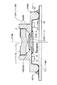
図1は本発明に係わる撮像装置の第1の実施の形態を示す斜視図であり、図2はその断面図である。図1および図2において、立体プリント基板1は、矩形台状の脚部1Aとその上の有底円筒形の胴部1Bからなり、脚部1Aと胴部1Bの境界には開口部1Cが形成され、脚部1Aの裏側にはプリント配線によるパターン22が形成されている。立体プリント基板1の胴部1Bの内周には、レンズ2が嵌め込まれ、その光軸17を中心にして、開口部1Cの上側に光学フィルター3が配置され、開口部1Cの下側に半導体撮像素子4およびチップ部品8が配置されている。これら構成部品は、立体プリント基板1に総て組み付けられて完成する構造となっている。そしてその下に、この立体プリント基板1が取り付けられる携帯電話、パソコン、各種センサーのメイン基板であるプリント基板13が配置される。
【0023】
次に、本実施の形態における撮像装置の組立順序を簡単に説明する。まず、立体プリント基板1の上方から、光学フィルター3を接着剤により固定し、次いで予め表面にレンズマスク6を設けたレンズ2を装着し、胴部1B内周上面に形成された接着ポイント(接着剤導入溝)5から接着剤を充填してレンズ2を固定する。充填された接着剤のうちの余分な量は、充填ポイント5下部の接着剤溜まり7に溜まる。次に、立体プリント基板1の下方から、半導体撮像素子4とLSIや抵抗、コンデンサー等のチップ部品8をパターン22に半田14または導電接着剤、超音波接合等で電気接続し、さらに脚部1Aをパターン22を介してプリント基板13のパターンに半田14または導電接着剤、超音波接合等で電気接続する。
【0024】
このように、本実施の形態1によれば、立体プリント基板1にレンズ2とその光軸17上に光学フィルター3、半導体撮像素子4を配置し、さらにチップ部品8を立体プリント基板1のパターン22に一体的に固定して構成することで、小型軽量で堅牢な構造とすることができる。また、自動機械での組み立てが可能であり、量産に適した構造とすることができる。さらに、立体プリント基板1にチップ部品8を搭載して、半導体撮像素子4の駆動や回路のデカップリングを行うことで、半導体撮像素子4の駆動回路との配線や部品を搭載した分だけリード線をなくして簡略化でき、リード線に流すクロック信号の波形のなまりや、デカップリングによる不要輻射を低減することもできる等の効果を有する。
【0025】
(実施の形態2)
図3は本発明に係わる撮像装置の第2の実施の形態を示す断面図であり、説明の便宜上、実施の形態1と同様な部材には同様な符号を付してある。図3において、立体プリント基板1は、矩形台形状の脚部1Aとその上の有底円筒形の胴部1Bからなり、脚部1Aと胴部1Bの境界には開口部1Cが形成され、さらに脚部1Aの内側には段部1Dが形成されている。この段部1Dを含めて、脚部1Aの裏側には配線パターン22が形成されている。立体プリント基板1の胴部1B内周には、レンズ2が嵌め込まれ、その光軸17を中心にして、開口部1Cの上部に光学フィルター3が配置され、開口部1Cの下部に半導体撮像素子4およびチップ部品8が配置されている。さらにその下の段部1Dに、LSI11aやチップ部品11bを片面または両面に搭載したプリント基板10が配置され、最後に携帯電話等のプリント基板13が配置される構造となっている。
【0026】
次に、本実施の形態2における撮像装置の組立順序を簡単に説明する。まず、立体プリント基板1の上方から、光学フィルター3を接着剤により固定し、次いで予め表面にレンズマスク6を形成されたレンズ2を装着して、胴部1B内周上面に形成された接着ポイント5から接着剤を充填してレンズ2を固定する。充填された接着剤のうちの余分な量は、充填ポイント5下部の接着剤溜まり7に溜まる。次に、立体プリント基板1の下方から、半導体撮像素子4とLSIあるいは抵抗やコンデンサーのチップ部品8をパターン22に半田14または導電接着剤、超音波接合等で電気接続し、さらに段部1Dのパターン22にプリント基板10を半田14または導電接着剤、超音波接合等で電気接続し、そして脚部1Aをパターン22を介してプリント基板13のパターンに半田14または導電接着剤、超音波接合等で電気接続する。
【0027】
このように、本実施の形態2によれば、立体プリント基板1にレンズ2とその光軸17上に光学フィルター3、半導体撮像素子4を配置し、さらにLSI11aやチップ部品11bを搭載したプリント基板10を立体プリント基板1のパターン22に一体的に固定して構成することで、上記実施の形態1の効果に加えて、撮像装置にさらに多くの機能を付加することができる。
【0028】
次に、上記第1および第2の実施の形態に共通の説明を行う。図4は立体プリント基板1の底面を示している。立体プリント基板1に対し、上方向と下方向より部品を接着と電気的接続により取り付けた撮像装置を、携帯電話、パソコン等のアプリケーションのプリント基板13に電気接続するために、半導体撮像素子4、プリント基板10等を電気的に接続したパターン22を、立体プリント基板1の底面18に沿って、また、立体プリント基板側面19にまで達するように、印刷あるいは張付け等により形成してある。このパターン22を介して、立体プリント基板底面18をアプリケーションのプリント基板13に配置して、半田、導電接着剤、超音波接合等の方法により電気的に接合して、半導体撮像素子により電気変換した映像信号をアプリケーションの本体に電気信号として出力する。
【0029】
図5は上記実施の形態における光学系を示している。入射光16は、レンズ2により集光され、赤外領域の感度を抑制する光学フィルター3を通って半導体撮像素子4に入射する。半導体撮像素子4の代表的な素子であるCCDの感度は、図6に示すように 光学フィルター3を通した特性Bとして可視光領域で感度特性が平坦になり、映像増幅回路23により増幅され、平坦な特性の映像信号としてカラー画像に対応している。図6に示すCCD感度特性において、光学フィルター3を通さない特性Aは、赤外領域で非常に高い感度を示しているので、暗いところの映像を撮像するときに赤外領域の感度を利用することで、暗いところでの映像や、赤外センサーとしても用いることができる。このため、図7に示すように、赤外領域の感度を抑制するための光学フィルター3を取り除き、レンズ2と半導体撮像素子4で撮像装置を構成することにより、高感度用撮像装置あるいは赤外センサーとして用いることができ、撮像装置の使用範囲を広げることができる。
【0030】
図8は上記実施の形態におけるレンズ2を立体プリント基板1に接着して固定する方法を示す図である。立体プリント基板1のレンズ2を挿入する内側に接着ポイント(接着剤導入溝)5を4個備えて接着作業を容易にする構造としている。接着ポイント5は、接着剤9の粘度に応じて設ける数を増減する構造とし、接着剤9の粘度が低いものを使うときは接着ポイント5の数を少なくして、少なくとも一箇所から接着剤9を点滴9aの形でスポイト12から接着ポイント5を通じて充填し、接着剤広がり9bとなってレンズ2を立体プリント基板1に接着する。接着剤9の粘度が高い場合は、複数の接着ポイント5から適量の接着剤9を点滴9aの形で充填する。本構造は撮像装置を自動機械で連続生産する際に、スポイト12からの点滴9aを効果的に行うのに適した構造である。
【0031】
図9はレンズ2を立体プリント基板1に接着する際に、接着剤9がレンズ2と立体プリント基板1の境目に浸透するように、立体プリント基板1の胴部内周面をテーパー15としたものである。こうすることで、撮像装置を連続生産する際に、接着ポイント5から充填された点滴9aがテーパー15を伝わって接着剤広がり9bとなり、レンズ2の周囲に均等に拡散して塗布されることとなる。またテーパー15は、自動機械で連続生産する場合に、レンズ2を上方から挿入してレンズ2を所定位置に装着する際に、テーパー15により自動機械の挿入公差に余裕を持たせることができ、すなわち上方から装着するときにテーパーに倣わせて余裕を持って挿入することができる。
【0032】
図10は乱射光による映像に対しての悪影響を最小限にするための構造を示している。レンズ2に入射光16が入力してレンズ2に集光されて半導体撮像素子4に合焦するときに、レンズ2表面の埃やレンズ2内の光の乱れによる乱反射光16aがレンズ側面2aに当たり反射され、入射光16が干渉されたり、半導体撮像素子4に到達したりして、映像の歪みや乱れが発生する可能性がある。これを防止するために、レンズ2の外面に接着する接着剤9を黒色系として、レンズ側面2aで反射しにくい色を採用することで、レンズ側面2aで内部の乱反射光16aの反射を抑制した光信号を半導体撮像素子4に出力できる。
【0033】
図11は余分に入った接着剤9の立体プリント基板内部への染みだしを防止した構造である。レンズ2と立体プリント基板1を接着剤で接着するときに、点滴9aの量が多すぎると、接着剤9が立体プリント基板1の内側に落ちて、レンズ接面1aから染みだし9cとなって内部を汚染するので、これを防ぐために、立体プリント基板1の胴部内周面の下部に接着剤溜まり7を設けたものである。
【0034】
図12はレンズ2のレンズ有効部以外のところに当たる光による影響を最小限にする構造である。レンズ2はガラスレンズより軽量で、非球面レンズとして屈折率を調整するために樹脂成形で製作されることが多い。樹脂成形のレンズの場合、図13に示すように、レンズ有効部2a以外の平面2bに入射光21a、21bが当たると、完全な鏡面状になっていないと、当たった光が表面の乱反射により内部に入り込み、乱反射光21cのようになり、入射光21に干渉したり、半導対撮像素子4に到達して映像が歪んだりして映像の品質を劣化させる。このため、図14に示すように、レンズ2の有効部2a以外の平面2bから光が入射しないように、平面2bに黒系統の塗料または金属材料によるレンズマスク6を設けた構造としたものである。
【0035】
このように、立体プリント基板1へのレンズ2、光学フィルター3、半導体撮像素子4、プリント基板10、13等の具体的な組立構造により、撮像装置を高いレベルで商品化することができ、またアプリケーションとの電気的接合をコネクター等を使用しない直接的な接続による構造とすることができる。なお、立体プリント基板1の底面と側面に備えたプリント配線パターン22を用いてアプリケーション基板に備えたコネクターに立体プリント基板を差し込んで電気接合を行う構造を採用しても良い。
【0036】
【発明の効果】
以上説明したように、本発明は、脚部とこの脚部上に設けられた筒状の胴部とを有する立体プリント基板を備え、前記脚部の裏面に半導体撮像素子を装着し、前記胴部の内部に前記撮像素子に光を入射させるためのレンズを保持した撮像装置において、前記立体プリント基板の前記胴部の内周面上部に接着剤を充填するための複数の接着剤導入溝を備え、前記立体プリント基板の前記胴部の内周面が、前記接着剤導入溝に連続して下部に向けて狭くなったテーパに形成されている。この構成により、接着剤導入溝に接着剤をスポイト状の治具で点滴することで、レンズの周囲に接着剤が均一に浸透して接着することができ、レンズを立体プリント基板に容易に固定できることとなる。また、接着剤を胴部内周面のレンズ周囲に容易に浸透させることができ、接着を正確に行うことができる。また、立体プリント基板にレンズを自動機械で装着するときに、レンズを上方から挿入する際に、またはレンズに対して立体プリント基板を下方から押し上げて装着する際に、挿入しやすい構造とすることができる。これにより、撮像装置に必要な総ての部品を立体プリント基板に集約して小型で軽量、堅固な撮像装置を実現できるとともに、自動機械により自動実装が可能であり、量産性に優れた組立方法を実現することができる。
【図面の簡単な説明】
【図1】本発明の実施の形態1における撮像装置の斜視図
【図2】本発明の実施の形態1における撮像装置の断面図
【図3】本発明の実施の形態2における撮像装置の断面図
【図4】本発明の実施の形態における立体プリントの底面を示す斜視図
【図5】本発明の実施の形態における光学系を示す模式図
【図6】本発明の実施の形態における半導体撮像素子の感度特性を示す特性図
【図7】本発明の実施の形態における別の光学系を示す模式図
【図8】本発明の実施の形態における接着剤充填方法を示す立体プリント基板の斜視図
【図9】本発明の実施の形態における接着剤充填方法を示す立体プリント基板の断面図
【図10】本発明の実施の形態における乱反射防止方法を示す立体プリント基板の断面図
【図11】本発明の実施の形態における接着剤染みだし防止方法を示す立体プリント基板の部分断面図
【図12】本発明の実施の形態におけるレンズマスクを示す立体プリント基板の斜視図
【図13】本発明の実施の形態におけるレンズマスクを設けないレンズの正面図
【図14】本発明の実施の形態におけるレンズマスクを設けたレンズの正面図
【符号の説明】
1 立体プリント基板
1A 脚部
1B 胴部
1C 開口部
1D 段部
2 レンズ
3 光学フィルター
4 半導体撮像素子
5 接着ポイント(接着剤導入溝)
6 レンズマスク
7 接着剤溜まり
8 チップ部品
9 接着剤
10 プリント基板
11a LSI
11b チップ部品
12 スポイト
13 プリント基板
14 半田
15 テーパ
16 入射光
17 光軸
18 立体プリント基板底面
19 立体プリント基板側面
22 パターン
23 映像増幅回路[0001]
BACKGROUND OF THE INVENTION
The present invention relates to an imaging device that is miniaturized using a semiconductor imaging device such as a surveillance camera, a medical camera, and an in-vehicle camera, and an assembling method thereof.
[0002]
[Prior art]
Conventionally, this type of image pickup apparatus has been used in various fields with the downsizing and high performance of semiconductor image pickup devices that convert images captured by lenses into electrical signals. In addition, the market for video input sensors is expanding due to the smaller cameras.
[0003]
In a conventional image pickup apparatus using a semiconductor image pickup device, components such as a lens, a semiconductor image pickup device, and an LSI are configured in a housing or a structure, and are combined. Moreover, the printed circuit board has a flat plate shape, and has a structure on which components necessary for driving the semiconductor image sensor are mounted.
[0004]
[Problems to be solved by the invention]
However, in such a conventional camera assembly method, even if the semiconductor image sensor is miniaturized, there is a limit to miniaturization in the structure in which each component is connected and assembled, and skill is required for assembly, or an automatic machine is used. There was a problem that it could not be assembled.
[0005]
The present invention solves such a conventional problem, and provides an imaging apparatus and an assembling method thereof that can be further miniaturized and assembled by an automatic machine.
[0006]
[Means for Solving the Problems]
The imaging device according to the present invention is formed at a boundary between a rectangular trapezoidal leg portion having a wiring pattern formed on the back surface, a bottomed cylindrical trunk portion provided on the leg portion, and the leg portion and the trunk portion. A three-dimensional printed circuit board having an opening, a semiconductor image sensor mounted on the back surface of the leg so as to close the opening, and a light that is held inside the body and is incident on the semiconductor image sensor And a lens . With this configuration, Ri can Do and that all the components necessary for the imaging apparatus can be miniaturized and integrated into the three-dimensional printed circuit board, that Do can be assembled by automatic machines.
[0008]
In addition, the imaging apparatus of the present invention includes an optical filter that is mounted on the body side of the opening so as to close the opening . With this configuration, it is possible to eliminate all the dedicated holding parts and joint assemblies for lenses, optical filters, semiconductor imaging devices, etc. that constitute the imaging device, and to reduce the size by consolidating everything on the three-dimensional printed circuit board. Become .
[0009]
The image pickup apparatus of the present invention is characterized in that a step portion having the wiring pattern formed on the leg portion is provided, and a printed circuit board in which an LSI and a chip component are bonded to one side or both sides is attached to the step portion. To do. With this configuration, more functions can be added to the imaging apparatus. In addition, the distance between the LSI that drives the semiconductor image sensor and the peripheral components can be shortened, and distortion of the clock signal waveform and unnecessary radiation can be prevented.
[0010]
In the imaging apparatus of the present invention , another printed circuit board is directly electrically connected to the wiring pattern formed on the bottom surface of the back surface of the leg portion of the three-dimensional printed circuit board . With this configuration, the assembled three-dimensional printed circuit board can be directly attached to the main circuit board of a mobile phone, a personal computer, and various sensors, and a lightweight structure can be realized because of the miniaturization and the need for connectors and the like.
[0011]
The image pickup apparatus of the present invention is characterized in that a wiring pattern formed on the back surface of the three-dimensional printed circuit board reaches the side surface of the three-dimensional printed circuit board . With this configuration, it is possible to perform electrical bonding by inserting a three-dimensional printed circuit board into a connector of another printed circuit board .
[0012]
In addition, the imaging apparatus of the present invention includes a three-dimensional printed circuit board having a leg portion and a cylindrical trunk portion provided on the leg portion, and a semiconductor imaging device is mounted on the back surface of the leg portion, and the trunk portion In the image pickup apparatus holding a lens for making light incident on the image pickup element, a plurality of adhesive introduction grooves for filling the upper part of the inner peripheral surface of the body part of the three-dimensional printed circuit board are provided. , the inner circumferential surface of the body portion of the three-dimensional printed circuit board, characterized in that it is formed in the taper narrows toward the bottom in succession to the adhesive introduction groove. With this configuration, by instilling the adhesive into the adhesive introduction groove with a dropper-shaped jig, the adhesive can uniformly penetrate and adhere to the periphery of the lens, and the lens can be easily fixed to a three-dimensional printed circuit board. It will be possible. Further, the adhesive can be easily permeated around the lens on the inner peripheral surface of the body portion, and the bonding can be performed accurately. Also, when mounting the lens on the 3D printed board with an automatic machine, when inserting the lens from above, or when pushing up the 3D printed board from below to mount it, the structure should be easy to insert Will be able to.
[0013]
Moreover, the imaging device of the present invention is characterized in that the adhesive is black. With this configuration, when turbulent light inside the lens reaches the lens side surface around the lens, it can be absorbed by the black color of the adhesive to prevent reflection on the lens side surface. As a result, the light incident on the lens is not directed in the direction of the optical axis in the lens due to the surface accuracy of the lens or adhering dust, and is reflected by the side surface of the lens to interfere with the light inside the lens. It is possible to prevent the image quality from being deteriorated or reaching the semiconductor image sensor.
[0017]
The imaging apparatus assembling method of the present invention includes a cylindrical body having a bottom, a rectangular trapezoidal leg having a wiring pattern formed on the inner surface of the back surface, and the trunk and the leg. For the three-dimensional printed circuit board having an opening formed at the boundary with the part, a lens is bonded to the inner peripheral surface of the body part, and then the wiring pattern is closed from the back side of the leg part. A semiconductor imaging element is bonded to the chip, and then a chip component is bonded to the wiring pattern. This makes it possible to clearly divide the manufacturing process by connecting parts from the top of the 3D printed circuit board by bonding, and electrically connecting parts from below by soldering, conductive adhesive, and ultrasonic bonding. This makes it easy to assemble and efficient production.
[0018]
In addition, the imaging apparatus assembly method of the present invention includes a cylindrical body with a bottom, a rectangular trapezoidal leg formed with a wiring pattern having a stepped portion on the inner side of the back surface, continuous to the body, For a three-dimensional printed circuit board having an opening formed at the boundary between the trunk and the leg, a lens is bonded to the inner peripheral surface of the trunk, and then the opening is closed from the back side of the leg. A semiconductor image pickup device is bonded to the wiring pattern, a chip component is bonded to the wiring pattern, and a printed circuit board having an LSI and a chip component bonded in advance on one or both sides is bonded to the stepped portion. Is. This makes it possible to clearly divide the manufacturing process by connecting parts from the top of the 3D printed circuit board by bonding, and electrically connecting parts from below by soldering, conductive adhesive, and ultrasonic bonding. This makes it easy to assemble and efficient production.
[0019]
The imaging apparatus assembling method of the present invention includes a cylindrical body having a bottom, a rectangular trapezoidal leg having a wiring pattern formed on the inner surface of the back surface, and the trunk and the leg. An optical filter is bonded to the three-dimensional printed circuit board having an opening formed at the boundary with the part so as to close the opening from the body side, and then a lens is bonded to the inner peripheral surface of the body part. Next, a semiconductor imaging device is joined to the wiring pattern so as to close the opening from the back side of the leg portion, and then a chip component is joined to the wiring pattern. This makes it possible to clearly divide the manufacturing process by connecting parts from the top of the 3D printed circuit board by bonding, and electrically connecting parts from below by soldering, conductive adhesive, and ultrasonic bonding. This makes it easy to assemble and efficient production.
[0020]
In addition, the imaging apparatus assembly method of the present invention includes a cylindrical body with a bottom, a rectangular trapezoidal leg formed with a wiring pattern having a stepped portion on the inner side of the back surface, continuous to the body, An optical filter is bonded to a three-dimensional printed circuit board having an opening formed at the boundary between the trunk and the leg so as to close the opening from the trunk, and then on the inner peripheral surface of the trunk A lens is joined, and then a semiconductor imaging device is joined to the wiring pattern so as to close the opening from the back side of the leg, then a chip component is joined to the wiring pattern, and the LSI is preliminarily attached to the stepped portion. A printed circuit board in which chip components are bonded to one side or both sides is bonded. This makes it possible to clearly divide the manufacturing process by connecting parts from the top of the 3D printed circuit board by bonding, and electrically connecting parts from below by soldering, conductive adhesive, and ultrasonic bonding. This makes it easy to assemble and efficient production.
[0021]
Further, the imaging apparatus assembly method of the present invention is characterized in that the assembled three-dimensional printed circuit board is joined to another printed circuit board via a wiring pattern formed on the bottom surface of the leg portion. As a result, a three-dimensional printed circuit board on which a lens, an optical filter, a semiconductor imaging device, an LSI, a chip component, and the like are mounted can be directly attached to the main substrate of a mobile phone, a personal computer, or various sensors.
[0022]
DETAILED DESCRIPTION OF THE INVENTION
Hereinafter, embodiments of the present invention will be described with reference to the drawings.
(Embodiment 1)
FIG. 1 is a perspective view showing a first embodiment of an imaging apparatus according to the present invention, and FIG. 2 is a sectional view thereof. 1 and 2, the three-dimensional printed circuit board 1 includes a rectangular trapezoidal leg 1A and a cylindrical body 1B with a bottom on the top, and an opening 1C is formed at the boundary between the leg 1A and the trunk 1B. A
[0023]
Next, the assembly order of the imaging device in this embodiment will be briefly described. First, the
[0024]
As described above, according to the first embodiment, the
[0025]
(Embodiment 2)
FIG. 3 is a cross-sectional view showing a second embodiment of the imaging apparatus according to the present invention. For convenience of explanation, the same reference numerals are given to the same members as those in the first embodiment. In FIG. 3, the three-dimensional printed circuit board 1 is composed of a rectangular trapezoidal leg 1A and a cylindrical body 1B with a bottom on the top, and an opening 1C is formed at the boundary between the leg 1A and the trunk 1B. Further, a step portion 1D is formed inside the leg portion 1A. A
[0026]
Next, the assembly order of the imaging device in the second embodiment will be briefly described. First, the
[0027]
As described above, according to the second embodiment, the printed circuit board in which the
[0028]
Next, a description common to the first and second embodiments will be given. FIG. 4 shows the bottom surface of the three-dimensional printed circuit board 1. In order to electrically connect an imaging device in which components are attached to the three-dimensional printed circuit board 1 from above and below by bonding and electrical connection to a printed circuit board 13 of an application such as a mobile phone or a personal computer, A
[0029]
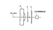
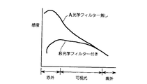
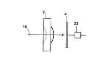
FIG. 5 shows the optical system in the above embodiment. The
[0030]
FIG. 8 is a diagram showing a method of adhering and fixing the
[0031]
FIG. 9 shows that the inner peripheral surface of the body of the three-dimensional printed circuit board 1 is tapered 15 so that the adhesive 9 penetrates the boundary between the
[0032]
FIG. 10 shows a structure for minimizing the adverse effect on the image due to the diffuse light. When incident light 16 is input to the
[0033]
FIG. 11 shows a structure in which excess adhesive 9 is prevented from oozing out into the three-dimensional printed circuit board. When the
[0034]
FIG. 12 shows a structure for minimizing the influence of light striking a portion other than the lens effective portion of the
[0035]
In this way, the imaging device can be commercialized at a high level by a specific assembly structure such as the
[0036]
【The invention's effect】
As described above, the present invention includes a three-dimensional printed circuit board having a leg portion and a cylindrical trunk portion provided on the leg portion, and a semiconductor imaging device is mounted on the back surface of the leg portion, In an image pickup apparatus that holds a lens for allowing light to enter the image pickup element inside a part, a plurality of adhesive introduction grooves for filling an adhesive on the inner peripheral surface of the body part of the three-dimensional printed circuit board are provided. And the inner peripheral surface of the body portion of the three-dimensional printed circuit board is formed in a taper that is continuous with the adhesive introduction groove and narrows toward the lower portion. With this configuration, the adhesive can be infiltrated uniformly around the lens by instilling the adhesive into the adhesive introduction groove with a dropper-shaped jig, and the lens can be easily fixed to the three-dimensional printed circuit board. It will be possible. Further, the adhesive can be easily permeated around the lens on the inner peripheral surface of the body portion, and the bonding can be performed accurately. Also, when mounting the lens on the 3D printed board with an automatic machine, when inserting the lens from above, or when pushing up the 3D printed board from below to mount it, the structure should be easy to insert Can do. As a result, all parts necessary for the imaging device can be collected on a 3D printed circuit board to realize a compact, lightweight, and robust imaging device, and can be automatically mounted by an automatic machine, and an assembly method with excellent mass productivity. Can be realized.
[Brief description of the drawings]
FIG. 1 is a perspective view of an image pickup apparatus according to Embodiment 1 of the present invention. FIG. 2 is a cross-sectional view of the image pickup apparatus according to Embodiment 1 of the present invention. FIG. 4 is a perspective view showing a bottom surface of a three-dimensional print according to an embodiment of the present invention. FIG. 5 is a schematic diagram showing an optical system according to the embodiment of the present invention. FIG. 7 is a schematic diagram showing another optical system in the embodiment of the present invention. FIG. 8 is a perspective view of a three-dimensional printed circuit board showing an adhesive filling method in the embodiment of the present invention. FIG. 9 is a cross-sectional view of a three-dimensional printed board showing an adhesive filling method in an embodiment of the present invention. FIG. 10 is a cross-sectional view of a three-dimensional printed board showing an irregular reflection preventing method in an embodiment of the present invention. In the embodiment of the invention FIG. 12 is a perspective view of a three-dimensional printed board showing a lens mask in an embodiment of the present invention. FIG. 13 is a lens mask in an embodiment of the present invention. FIG. 14 is a front view of a lens provided with a lens mask according to an embodiment of the present invention.
DESCRIPTION OF SYMBOLS 1 3D printed circuit board 1A Leg part 1B Trunk part 1C Opening part
6
11b Chip component 12 Dropper 13 Printed
Claims (2)
前記立体プリント基板の前記胴部の内周面上部に接着剤を充填するための複数の接着剤導入溝を備え、
前記立体プリント基板の前記胴部の内周面が、前記接着剤導入溝に連続して下部に向けて狭くなったテーパに形成されていることを特徴とする撮像装置。A three-dimensional printed circuit board having a leg portion and a cylindrical trunk portion provided on the leg portion; a semiconductor image pickup device mounted on a back surface of the leg portion; In an imaging device holding a lens for incidence,
A plurality of adhesive introduction grooves for filling an adhesive on the inner peripheral surface upper part of the body portion of the three-dimensional printed circuit board,
An imaging apparatus, wherein an inner peripheral surface of the body portion of the three-dimensional printed circuit board is formed in a taper that is narrowed toward a lower portion continuously from the adhesive introduction groove.
Priority Applications (5)
| Application Number | Priority Date | Filing Date | Title |
|---|---|---|---|
| JP2000053400A JP4004705B2 (en) | 2000-02-29 | 2000-02-29 | Imaging device and imaging device assembling method |
| EP01906306A EP1289281A4 (en) | 2000-02-29 | 2001-02-26 | Image pickup device, and image pickup device assembling method |
| CNB018056903A CN1281050C (en) | 2000-02-29 | 2001-02-26 | Image pickup device, and image pickup device assembling method |
| US10/169,359 US7333147B2 (en) | 2000-02-29 | 2001-02-26 | Image pickup device with a three-dimensional circuit board and device assembly method |
| PCT/JP2001/001415 WO2001065836A1 (en) | 2000-02-29 | 2001-02-26 | Image pickup device, and image pickup device assembling method |
Applications Claiming Priority (1)
| Application Number | Priority Date | Filing Date | Title |
|---|---|---|---|
| JP2000053400A JP4004705B2 (en) | 2000-02-29 | 2000-02-29 | Imaging device and imaging device assembling method |
Publications (2)
| Publication Number | Publication Date |
|---|---|
| JP2001245186A JP2001245186A (en) | 2001-09-07 |
| JP4004705B2 true JP4004705B2 (en) | 2007-11-07 |
Family
ID=18574792
Family Applications (1)
| Application Number | Title | Priority Date | Filing Date |
|---|---|---|---|
| JP2000053400A Expired - Lifetime JP4004705B2 (en) | 2000-02-29 | 2000-02-29 | Imaging device and imaging device assembling method |
Country Status (5)
| Country | Link |
|---|---|
| US (1) | US7333147B2 (en) |
| EP (1) | EP1289281A4 (en) |
| JP (1) | JP4004705B2 (en) |
| CN (1) | CN1281050C (en) |
| WO (1) | WO2001065836A1 (en) |
Families Citing this family (99)
| Publication number | Priority date | Publication date | Assignee | Title |
|---|---|---|---|---|
| JP3773177B2 (en) | 2001-11-30 | 2006-05-10 | 松下電器産業株式会社 | Solid-state imaging device and manufacturing method thereof |
| KR100877159B1 (en) | 2001-11-30 | 2009-01-07 | 파나소닉 주식회사 | Solid-state imaging apparatus and manufacturing method thereof |
| JP3787765B2 (en) * | 2001-11-30 | 2006-06-21 | 松下電器産業株式会社 | Solid-state imaging device and manufacturing method thereof |
| US6825540B2 (en) * | 2001-12-05 | 2004-11-30 | Matsushita Electric Industrial Co., Ltd. | Miniaturized, resin-sealed solid state imaging apparatus |
| JP4096588B2 (en) * | 2002-03-22 | 2008-06-04 | コニカミノルタホールディングス株式会社 | Imaging device |
| US7652895B2 (en) | 2002-04-11 | 2010-01-26 | Tpo Displays Corp. | Electrically insulating body, and electronic device |
| KR100514917B1 (en) | 2002-05-07 | 2005-09-14 | 미쓰이 가가쿠 가부시키가이샤 | Package for mounting a solid state image sensor |
| US20060061008A1 (en) | 2004-09-14 | 2006-03-23 | Lee Karner | Mounting assembly for vehicle interior mirror |
| CN1675967A (en) * | 2002-08-05 | 2005-09-28 | 皇家飞利浦电子股份有限公司 | An electronic product, a body and a method of manufacturing |
| JP4398863B2 (en) * | 2002-09-30 | 2010-01-13 | 統寶光電股▲分▼有限公司 | How to assemble the camera module |
| JP3813944B2 (en) | 2003-04-28 | 2006-08-23 | 松下電器産業株式会社 | Imaging device |
| JP4510403B2 (en) * | 2003-05-08 | 2010-07-21 | 富士フイルム株式会社 | Camera module and method for manufacturing camera module |
| US7122787B2 (en) | 2003-05-09 | 2006-10-17 | Matsushita Electric Industrial Co., Ltd. | Imaging apparatus with three dimensional circuit board |
| JP4525000B2 (en) * | 2003-05-09 | 2010-08-18 | ソニー株式会社 | Optical device, lens barrel and imaging device |
| JP3981348B2 (en) | 2003-05-30 | 2007-09-26 | 松下電器産業株式会社 | Imaging device and manufacturing method thereof |
| KR100568223B1 (en) * | 2003-06-18 | 2006-04-07 | 삼성전자주식회사 | Solid-State Imaging Apparatus |
| US7141884B2 (en) | 2003-07-03 | 2006-11-28 | Matsushita Electric Industrial Co., Ltd. | Module with a built-in semiconductor and method for producing the same |
| EP1670238B1 (en) * | 2003-09-30 | 2010-11-10 | Fujitsu Semiconductor Limited | Camera module |
| JP4347674B2 (en) * | 2003-12-01 | 2009-10-21 | 株式会社ミツトヨ | Lens holding structure, objective lens, optical microscope and assembly method |
| KR20050067081A (en) | 2003-12-26 | 2005-06-30 | 교세라 가부시키가이샤 | Camera module and portable terminal equipped with the camera module |
| JP3906844B2 (en) * | 2004-01-13 | 2007-04-18 | ソニー株式会社 | Imaging device |
| JP2005208351A (en) * | 2004-01-22 | 2005-08-04 | Seiko Precision Inc | Solid state imaging device, and portable electronic equipment equipped with the same |
| JP2005266586A (en) * | 2004-03-19 | 2005-09-29 | Olympus Corp | Imaging device and its manufacturing method |
| JP2005286888A (en) * | 2004-03-30 | 2005-10-13 | Fuji Photo Film Co Ltd | Solid-state imaging apparatus |
| JP2005351948A (en) * | 2004-06-08 | 2005-12-22 | Konica Minolta Opto Inc | Imaging apparatus and personal digital assistant equipped with the same |
| JP4699714B2 (en) * | 2004-06-15 | 2011-06-15 | 富士フイルム株式会社 | Eccentricity measuring apparatus and eccentricity measuring method |
| JP4578168B2 (en) * | 2004-07-23 | 2010-11-10 | パナソニック株式会社 | Method for manufacturing solid-state imaging device |
| DE102004056946A1 (en) | 2004-11-23 | 2006-05-24 | Karl Storz Gmbh & Co. Kg | Image pick-up module and method of assembling an image pick-up module |
| JP4677534B2 (en) * | 2005-01-25 | 2011-04-27 | シコー株式会社 | Lens drive device |
| JP2006227378A (en) * | 2005-02-18 | 2006-08-31 | Sony Corp | Lens barrel and imaging apparatus |
| JP2006245246A (en) * | 2005-03-02 | 2006-09-14 | Sharp Corp | Solid state imaging apparatus |
| US8698894B2 (en) | 2006-02-07 | 2014-04-15 | Magna Electronics Inc. | Camera mounted at rear of vehicle |
| JP4107347B2 (en) * | 2006-03-22 | 2008-06-25 | 株式会社村田製作所 | Infrared sensor and method of manufacturing infrared sensor |
| US7990727B1 (en) * | 2006-04-03 | 2011-08-02 | Aprolase Development Co., Llc | Ball grid array stack |
| JP4657974B2 (en) | 2006-05-09 | 2011-03-23 | パナソニック株式会社 | Card type MEMS microphone |
| JP4638837B2 (en) * | 2006-05-30 | 2011-02-23 | 日本電気硝子株式会社 | Optical component and light emitting device |
| JP2007324239A (en) * | 2006-05-30 | 2007-12-13 | Nichia Chem Ind Ltd | Light-emitting device |
| JP2008011144A (en) * | 2006-06-29 | 2008-01-17 | Matsushita Electric Ind Co Ltd | Imaging apparatus |
| JP5066734B2 (en) * | 2006-06-30 | 2012-11-07 | シコー株式会社 | Lens driving device, camera and camera-equipped mobile phone |
| JP4942187B2 (en) * | 2006-06-30 | 2012-05-30 | シコー株式会社 | Lens driving device, camera and camera-equipped mobile phone |
| JP2008092532A (en) * | 2006-10-05 | 2008-04-17 | Matsushita Electric Ind Co Ltd | Imaging apparatus, manufacturing method therefor and mobile phone unit |
| JP2008124923A (en) * | 2006-11-14 | 2008-05-29 | Matsushita Electric Works Ltd | Camera module |
| JP2008148222A (en) * | 2006-12-13 | 2008-06-26 | Matsushita Electric Ind Co Ltd | Solid state imaging apparatus and its manufacturing method |
| US20100045846A1 (en) * | 2007-02-02 | 2010-02-25 | Hiroshi Nishizawa | Image pickup device, method of manufacturing the same, and mobile terminal device |
| JP4663666B2 (en) * | 2007-03-08 | 2011-04-06 | パナソニック株式会社 | Imaging device, manufacturing method thereof, and portable terminal device |
| JP4663667B2 (en) * | 2007-03-08 | 2011-04-06 | パナソニック株式会社 | Imaging device, manufacturing method thereof, and portable terminal device |
| JP4712737B2 (en) * | 2007-02-02 | 2011-06-29 | パナソニック株式会社 | Imaging device, manufacturing method thereof, and portable terminal device |
| WO2008096584A1 (en) * | 2007-02-07 | 2008-08-14 | Konica Minolta Opto, Inc. | Imaging device manufacturing method, imaging device and portable terminal |
| JP4850086B2 (en) * | 2007-02-14 | 2012-01-11 | パナソニック株式会社 | MEMS microphone device |
| JP5047679B2 (en) | 2007-04-26 | 2012-10-10 | オリンパスメディカルシステムズ株式会社 | Imaging unit and method for manufacturing the imaging unit |
| JP2008292776A (en) * | 2007-05-25 | 2008-12-04 | Nidec Sankyo Corp | Lens drive device |
| KR100860308B1 (en) * | 2007-06-05 | 2008-09-25 | 삼성전기주식회사 | Camera module package and method of manufacturing the same |
| CN101349792B (en) * | 2007-07-18 | 2011-11-09 | 鸿富锦精密工业(深圳)有限公司 | Lens mount and lens mount components used thereby |
| CN100576555C (en) * | 2007-08-09 | 2009-12-30 | 佛山普立华科技有限公司 | Device for image |
| CN101436603B (en) * | 2007-11-14 | 2010-11-10 | 鸿富锦精密工业(深圳)有限公司 | Imaging die set |
| US9350976B2 (en) | 2007-11-26 | 2016-05-24 | First Sensor Mobility Gmbh | Imaging unit of a camera for recording the surroundings with optics uncoupled from a circuit board |
| DE102007057172B4 (en) * | 2007-11-26 | 2009-07-02 | Silicon Micro Sensors Gmbh | Stereo camera for environmental detection |
| JP2009145598A (en) * | 2007-12-13 | 2009-07-02 | Sharp Corp | Solid state image pickup device and electronic device including the same |
| EP2094000A3 (en) * | 2008-02-22 | 2013-06-05 | Silicon Micro Sensors GmbH | Imaging device of a camera |
| KR101567067B1 (en) * | 2008-12-02 | 2015-11-06 | 엘지이노텍 주식회사 | Camera Module |
| JP5047220B2 (en) * | 2009-04-30 | 2012-10-10 | パナソニック株式会社 | Camera device and method of manufacturing camera device |
| KR101626132B1 (en) * | 2009-09-28 | 2016-05-31 | 엘지이노텍 주식회사 | unified Camera module |
| JP5289582B2 (en) * | 2009-11-26 | 2013-09-11 | 京セラ株式会社 | Imaging device and imaging device module |
| JP2011128556A (en) * | 2009-12-21 | 2011-06-30 | Panasonic Electric Works Co Ltd | Camera module and method for manufacturing the same |
| WO2011114847A1 (en) * | 2010-03-16 | 2011-09-22 | コニカミノルタオプト株式会社 | Imaging device and portable terminal |
| CN102893593B (en) * | 2010-06-28 | 2016-11-23 | 京瓷株式会社 | Circuit board and camera head and camera module |
| US9264672B2 (en) | 2010-12-22 | 2016-02-16 | Magna Mirrors Of America, Inc. | Vision display system for vehicle |
| JP2013057764A (en) * | 2011-09-07 | 2013-03-28 | Olympus Imaging Corp | Holding frame, optical element holding unit, lens barrel unit and imaging apparatus |
| TWI505704B (en) * | 2011-09-14 | 2015-10-21 | Hon Hai Prec Ind Co Ltd | Method for manufacturing camera module and camera module |
| CN102998765B (en) * | 2011-09-16 | 2016-01-20 | 鸿富锦精密工业(深圳)有限公司 | Camera module group assembling method and camera module |
| JP5797852B2 (en) | 2011-11-18 | 2015-10-21 | ハネウェル・インターナショナル・インコーポレーテッド | Fabrication of 3D printed circuit board structure |
| US20150198484A1 (en) * | 2012-07-06 | 2015-07-16 | Pricer Ab | Electronic shelf label with an optical arrangement |
| US9571707B2 (en) * | 2013-07-17 | 2017-02-14 | Canon Kabushiki Kaisha | Image pickup apparatus having decreased thickness in the vertical direction |
| JP6051399B2 (en) * | 2014-07-17 | 2016-12-27 | 関根 弘一 | Solid-state imaging device and manufacturing method thereof |
| US9955054B2 (en) | 2015-02-05 | 2018-04-24 | Robert Bosch Gmbh | Camera and method for assembling with fixed final alignment |
| JP2016148812A (en) * | 2015-02-13 | 2016-08-18 | アルプス電気株式会社 | Lens drive device |
| JP2016202830A (en) * | 2015-04-28 | 2016-12-08 | オリンパス株式会社 | Endoscope distal end portion and endoscope |
| WO2016203797A1 (en) * | 2015-06-16 | 2016-12-22 | オリンパス株式会社 | Imaging module, endoscope system, and method for manufacturing imaging module |
| CN105445888B (en) * | 2015-12-21 | 2020-04-03 | 宁波舜宇光电信息有限公司 | Adjustable optical lens, camera module and calibration method thereof |
| EP3166146B1 (en) * | 2015-11-06 | 2019-04-17 | ams AG | Optical package and method of producing an optical package |
| CN108293088B (en) * | 2015-12-02 | 2021-04-13 | 微型模块科技株式会社 | Optical device and method for manufacturing optical device |
| WO2017141369A1 (en) * | 2016-02-17 | 2017-08-24 | オリンパス株式会社 | Optical transmission module, and endoscope |
| CN109328318B (en) * | 2016-04-15 | 2021-11-02 | 赫普塔冈微光有限公司 | Optoelectronic module with alignment spacers and method for assembling the optoelectronic module |
| EP3477935A4 (en) | 2016-06-23 | 2020-02-26 | Ningbo Sunny Opotech Co., Ltd. | Fixed-focus photographing module and focusing device and method thereof |
| JP2018045212A (en) * | 2016-09-16 | 2018-03-22 | 株式会社フジクラ | Image capturing module and manufacturing method therefor |
| WO2018061295A1 (en) * | 2016-09-28 | 2018-04-05 | シャープ株式会社 | Optical apparatus and camera module |
| KR102402614B1 (en) * | 2017-03-08 | 2022-05-27 | 엘지이노텍 주식회사 | Camera module including liquid lens, optical device including the same |
| CN111051950B (en) * | 2017-11-10 | 2021-09-21 | 华为技术有限公司 | Lens assembly, camera assembly and terminal |
| FR3073980A1 (en) * | 2017-11-23 | 2019-05-24 | Stmicroelectronics (Grenoble 2) Sas | ENCAPSULATION COVER FOR ELECTRONIC HOUSING AND METHOD OF MANUFACTURE |
| FR3075466B1 (en) * | 2017-12-15 | 2020-05-29 | Stmicroelectronics (Grenoble 2) Sas | ELECTRONIC CIRCUIT BOX COVER |
| FR3075465B1 (en) | 2017-12-15 | 2020-03-27 | Stmicroelectronics (Grenoble 2) Sas | ELECTRONIC CIRCUIT BOX COVER |
| FR3078855A1 (en) * | 2018-03-08 | 2019-09-13 | St Microelectronics Grenoble 2 Sas | ENCAPSULATION COVER FOR ELECTRONIC HOUSING AND METHOD OF MANUFACTURE |
| JP6641415B2 (en) * | 2018-05-01 | 2020-02-05 | アルプスアルパイン株式会社 | Lens drive |
| WO2019231239A1 (en) * | 2018-05-29 | 2019-12-05 | 엘지이노텍(주) | Lens driving device, camera device, and optical apparatus including same |
| KR102500654B1 (en) * | 2018-05-29 | 2023-02-16 | 엘지이노텍 주식회사 | A camera apparatus and optical instrument including the same |
| WO2020034171A1 (en) * | 2018-08-17 | 2020-02-20 | 深圳市汇顶科技股份有限公司 | Optical sensing module and manufacturing method therefor |
| JP7191373B2 (en) * | 2018-11-16 | 2022-12-19 | マイクロモジュールテクノロジー株式会社 | OPTICAL DEVICE, SPECTRAL SENSOR MODULE, IMAGING MODULE, AND OPTICAL DEVICE MANUFACTURING METHOD |
| JP7222424B2 (en) * | 2019-05-22 | 2023-02-15 | 日本電信電話株式会社 | Waveguide connection structure, waveguide chip, connector, manufacturing method of waveguide connection part, and waveguide connection method |
| GB2605781A (en) * | 2021-04-09 | 2022-10-19 | Aptiv Tech Ltd | Method of assembling an optical device and optical device assembled according to the same |
Family Cites Families (31)
| Publication number | Priority date | Publication date | Assignee | Title |
|---|---|---|---|---|
| JPS6132017A (en) * | 1984-07-23 | 1986-02-14 | Olympus Optical Co Ltd | Lens holding device |
| JPS6343353A (en) * | 1986-08-08 | 1988-02-24 | Olympus Optical Co Ltd | Solid-state image sensing device |
| JP2765925B2 (en) | 1989-03-17 | 1998-06-18 | 株式会社日立製作所 | Video camera unit |
| JPH0698121B2 (en) | 1989-06-09 | 1994-12-07 | 富士写真光機株式会社 | Solid-state image sensor assembly for electronic endoscope |
| JPH05176208A (en) | 1991-10-14 | 1993-07-13 | Sony Corp | Video camera |
| JPH07272302A (en) * | 1994-03-31 | 1995-10-20 | Matsushita Electric Ind Co Ltd | Objective lens device |
| KR970705294A (en) * | 1995-05-31 | 1997-09-06 | 이데이 노부유키 | Image pickup apparatus, image pickup adapter apparatus, signal processing apparatus, signal processing method, information processing apparatus, and information processing method Processing Apparatus, and Information Processing Method) |
| JPH1010394A (en) | 1996-04-26 | 1998-01-16 | Chiyuugai Oputoronikusu Kk | Electronic image pickup device |
| US6795120B2 (en) * | 1996-05-17 | 2004-09-21 | Sony Corporation | Solid-state imaging apparatus and camera using the same |
| JPH1114878A (en) | 1997-06-25 | 1999-01-22 | Matsushita Electron Corp | Image pickup device |
| JP3836235B2 (en) * | 1997-12-25 | 2006-10-25 | 松下電器産業株式会社 | Solid-state imaging device and manufacturing method thereof |
| JP3582634B2 (en) * | 1998-04-10 | 2004-10-27 | 松下電器産業株式会社 | Solid-state imaging device |
| JPH11341365A (en) | 1998-05-22 | 1999-12-10 | Sony Corp | Package structure for image-pickup element and structure for attaching the image-pickup element to lens barrel using the package structure |
| JPH11341366A (en) * | 1998-05-26 | 1999-12-10 | Sony Corp | Package structure for image-pickup element and structure for attaching the image-pickup element to lens barrel using the package structure |
| JP4372241B2 (en) * | 1998-08-05 | 2009-11-25 | パナソニック株式会社 | Method for manufacturing solid-state imaging device |
| US6762796B1 (en) * | 1998-08-10 | 2004-07-13 | Olympus Optical Co., Ltd. | Image pickup module having integrated lens and semiconductor chip |
| JP3201381B2 (en) | 1999-04-12 | 2001-08-20 | セイコーエプソン株式会社 | Semiconductor thin film manufacturing method |
| JP2001203913A (en) * | 2000-01-21 | 2001-07-27 | Sony Corp | Image pickup device, camera module, and camera system |
| JP3887162B2 (en) * | 2000-10-19 | 2007-02-28 | 富士通株式会社 | Imaging semiconductor device |
| JP2002252797A (en) * | 2001-02-26 | 2002-09-06 | Sony Corp | Solid-state image pickup device |
| JP3646933B2 (en) * | 2001-11-22 | 2005-05-11 | 松下電器産業株式会社 | Solid-state imaging device and manufacturing method thereof |
| JP2004103860A (en) * | 2002-09-10 | 2004-04-02 | Fujitsu Ltd | Semiconductor device, camera module and its manufacturing method |
| TW558064U (en) * | 2002-09-23 | 2003-10-11 | Ist Internat Semiconductor Tec | Thin type camera module |
| US20040150740A1 (en) * | 2003-01-30 | 2004-08-05 | Hsin Chung Hsien | Miniaturized image sensor module |
| US7122787B2 (en) * | 2003-05-09 | 2006-10-17 | Matsushita Electric Industrial Co., Ltd. | Imaging apparatus with three dimensional circuit board |
| US6953891B2 (en) * | 2003-09-16 | 2005-10-11 | Micron Technology, Inc. | Moisture-resistant electronic device package and methods of assembly |
| JP2005176208A (en) | 2003-12-15 | 2005-06-30 | Kyocera Corp | Mobile communication terminal |
| US7253388B2 (en) * | 2004-04-23 | 2007-08-07 | Hymite A/S | Assembly with self-alignment features to position a cover on a substrate that supports a micro component |
| JP2005345571A (en) * | 2004-05-31 | 2005-12-15 | Canon Inc | Image pickup unit and electronic equipment |
| US7262405B2 (en) * | 2004-06-14 | 2007-08-28 | Micron Technology, Inc. | Prefabricated housings for microelectronic imagers |
| US20060016973A1 (en) * | 2004-07-21 | 2006-01-26 | Advanced Semiconductor Engineering, Inc. | Multi-chip image sensor package module |
-
2000
- 2000-02-29 JP JP2000053400A patent/JP4004705B2/en not_active Expired - Lifetime
-
2001
- 2001-02-26 CN CNB018056903A patent/CN1281050C/en not_active Expired - Lifetime
- 2001-02-26 US US10/169,359 patent/US7333147B2/en not_active Expired - Lifetime
- 2001-02-26 WO PCT/JP2001/001415 patent/WO2001065836A1/en not_active Application Discontinuation
- 2001-02-26 EP EP01906306A patent/EP1289281A4/en not_active Withdrawn
Also Published As
| Publication number | Publication date |
|---|---|
| EP1289281A4 (en) | 2006-06-14 |
| EP1289281A1 (en) | 2003-03-05 |
| JP2001245186A (en) | 2001-09-07 |
| US20050270403A1 (en) | 2005-12-08 |
| CN1406432A (en) | 2003-03-26 |
| CN1281050C (en) | 2006-10-18 |
| WO2001065836A1 (en) | 2001-09-07 |
| US7333147B2 (en) | 2008-02-19 |
Similar Documents
| Publication | Publication Date | Title |
|---|---|---|
| JP4004705B2 (en) | Imaging device and imaging device assembling method | |
| US12022180B2 (en) | Array camera module and application thereof | |
| CN108401094B (en) | Array camera module, molding photosensitive assembly and manufacturing method thereof and electronic equipment with array camera module | |
| TWI703715B (en) | Array camera module, molded photosensitive element and manufacturing method thereof, and electronic equipment | |
| CA2571345C (en) | System and method for mounting an image capture device on a flexible substrate | |
| JP4698874B2 (en) | Image sensor module and method of manufacturing image sensor module | |
| JP3846158B2 (en) | Lens barrel and imaging apparatus using the same | |
| KR100741344B1 (en) | Optical device module, and method of fabricating the optical device module | |
| TW523922B (en) | Small type module for taking picture | |
| EP1465411A2 (en) | Compact camera module | |
| CN109581785B (en) | Camera module for reducing stray light and photosensitive assembly thereof | |
| CN108401091B (en) | Camera module and molded circuit board assembly and application thereof | |
| JPH0775400B2 (en) | Camera head of solid-state imaging device and method of manufacturing the same | |
| CA2654422A1 (en) | Camera module with premolded lens housing and method of manufacture | |
| JP3417225B2 (en) | Solid-state imaging device and camera using it | |
| JPH09102896A (en) | Image pickup element assembly for electronic endoscope | |
| US20190394366A1 (en) | Imaging chip packaging structure and camera device having the same | |
| KR20110002266A (en) | Photographing module | |
| CN107734216B (en) | Array camera module, molding photosensitive assembly and manufacturing method thereof and electronic equipment with array camera module | |
| JP2002204400A (en) | Imaging element module with lens | |
| CN109672806B (en) | Camera module, photosensitive assembly and packaging method thereof | |
| JP2008160757A (en) | Imaging apparatus | |
| JP3181503B2 (en) | Electronic endoscope image sensor assembly | |
| JP5152695B2 (en) | Manufacturing method of imaging apparatus | |
| KR100847849B1 (en) | Camera module |
Legal Events
| Date | Code | Title | Description |
|---|---|---|---|
| A131 | Notification of reasons for refusal |
Free format text: JAPANESE INTERMEDIATE CODE: A131 Effective date: 20051108 |
|
| A521 | Request for written amendment filed |
Free format text: JAPANESE INTERMEDIATE CODE: A523 Effective date: 20051227 |
|
| A02 | Decision of refusal |
Free format text: JAPANESE INTERMEDIATE CODE: A02 Effective date: 20070320 |
|
| A521 | Request for written amendment filed |
Free format text: JAPANESE INTERMEDIATE CODE: A523 Effective date: 20070418 |
|
| A911 | Transfer to examiner for re-examination before appeal (zenchi) |
Free format text: JAPANESE INTERMEDIATE CODE: A911 Effective date: 20070605 |
|
| TRDD | Decision of grant or rejection written | ||
| A01 | Written decision to grant a patent or to grant a registration (utility model) |
Free format text: JAPANESE INTERMEDIATE CODE: A01 Effective date: 20070731 |
|
| A61 | First payment of annual fees (during grant procedure) |
Free format text: JAPANESE INTERMEDIATE CODE: A61 Effective date: 20070822 |
|
| R150 | Certificate of patent or registration of utility model |
Ref document number: 4004705 Country of ref document: JP Free format text: JAPANESE INTERMEDIATE CODE: R150 Free format text: JAPANESE INTERMEDIATE CODE: R150 |
|
| FPAY | Renewal fee payment (event date is renewal date of database) |
Free format text: PAYMENT UNTIL: 20100831 Year of fee payment: 3 |
|
| FPAY | Renewal fee payment (event date is renewal date of database) |
Free format text: PAYMENT UNTIL: 20110831 Year of fee payment: 4 |
|
| FPAY | Renewal fee payment (event date is renewal date of database) |
Free format text: PAYMENT UNTIL: 20110831 Year of fee payment: 4 |
|
| FPAY | Renewal fee payment (event date is renewal date of database) |
Free format text: PAYMENT UNTIL: 20120831 Year of fee payment: 5 |
|
| FPAY | Renewal fee payment (event date is renewal date of database) |
Free format text: PAYMENT UNTIL: 20130831 Year of fee payment: 6 |
|
| EXPY | Cancellation because of completion of term |