WO2016203797A1 - Imaging module, endoscope system, and method for manufacturing imaging module - Google Patents
Imaging module, endoscope system, and method for manufacturing imaging module Download PDFInfo
- Publication number
- WO2016203797A1 WO2016203797A1 PCT/JP2016/058006 JP2016058006W WO2016203797A1 WO 2016203797 A1 WO2016203797 A1 WO 2016203797A1 JP 2016058006 W JP2016058006 W JP 2016058006W WO 2016203797 A1 WO2016203797 A1 WO 2016203797A1
- Authority
- WO
- WIPO (PCT)
- Prior art keywords
- circuit board
- imaging module
- connection
- chip size
- size package
- Prior art date
Links
- 238000003384 imaging method Methods 0.000 title claims abstract description 118
- 238000004519 manufacturing process Methods 0.000 title claims abstract description 9
- 238000000034 method Methods 0.000 title claims abstract description 5
- 230000003287 optical effect Effects 0.000 claims abstract description 21
- 238000003780 insertion Methods 0.000 claims description 16
- 230000037431 insertion Effects 0.000 claims description 16
- 229910000679 solder Inorganic materials 0.000 claims description 16
- 238000007789 sealing Methods 0.000 claims description 2
- 239000003795 chemical substances by application Substances 0.000 description 73
- 238000012986 modification Methods 0.000 description 22
- 230000004048 modification Effects 0.000 description 22
- 239000000758 substrate Substances 0.000 description 15
- 238000010586 diagram Methods 0.000 description 14
- 238000005286 illumination Methods 0.000 description 8
- 230000010365 information processing Effects 0.000 description 8
- 238000005452 bending Methods 0.000 description 7
- 239000000835 fiber Substances 0.000 description 4
- 239000011521 glass Substances 0.000 description 4
- 230000000149 penetrating effect Effects 0.000 description 4
- 230000002093 peripheral effect Effects 0.000 description 3
- 239000010703 silicon Substances 0.000 description 3
- 229910052710 silicon Inorganic materials 0.000 description 3
- 239000004593 Epoxy Substances 0.000 description 2
- XUIMIQQOPSSXEZ-UHFFFAOYSA-N Silicon Chemical compound [Si] XUIMIQQOPSSXEZ-UHFFFAOYSA-N 0.000 description 2
- 239000000919 ceramic Substances 0.000 description 2
- 239000006059 cover glass Substances 0.000 description 2
- 238000005401 electroluminescence Methods 0.000 description 2
- 238000001727 in vivo Methods 0.000 description 2
- 238000002347 injection Methods 0.000 description 2
- 239000007924 injection Substances 0.000 description 2
- XLYOFNOQVPJJNP-UHFFFAOYSA-N water Substances O XLYOFNOQVPJJNP-UHFFFAOYSA-N 0.000 description 2
- 239000000853 adhesive Substances 0.000 description 1
- 230000001070 adhesive effect Effects 0.000 description 1
- 230000015572 biosynthetic process Effects 0.000 description 1
- 239000003990 capacitor Substances 0.000 description 1
- 238000005553 drilling Methods 0.000 description 1
- 238000010438 heat treatment Methods 0.000 description 1
- 238000001746 injection moulding Methods 0.000 description 1
- 239000004973 liquid crystal related substance Substances 0.000 description 1
- 239000013307 optical fiber Substances 0.000 description 1
- 239000011347 resin Substances 0.000 description 1
- 229920005989 resin Polymers 0.000 description 1
- 239000004065 semiconductor Substances 0.000 description 1
- 230000001225 therapeutic effect Effects 0.000 description 1
Images


Classifications
-
- A—HUMAN NECESSITIES
- A61—MEDICAL OR VETERINARY SCIENCE; HYGIENE
- A61B—DIAGNOSIS; SURGERY; IDENTIFICATION
- A61B1/00—Instruments for performing medical examinations of the interior of cavities or tubes of the body by visual or photographical inspection, e.g. endoscopes; Illuminating arrangements therefor
- A61B1/04—Instruments for performing medical examinations of the interior of cavities or tubes of the body by visual or photographical inspection, e.g. endoscopes; Illuminating arrangements therefor combined with photographic or television appliances
- A61B1/05—Instruments for performing medical examinations of the interior of cavities or tubes of the body by visual or photographical inspection, e.g. endoscopes; Illuminating arrangements therefor combined with photographic or television appliances characterised by the image sensor, e.g. camera, being in the distal end portion
- A61B1/051—Details of CCD assembly
-
- A—HUMAN NECESSITIES
- A61—MEDICAL OR VETERINARY SCIENCE; HYGIENE
- A61B—DIAGNOSIS; SURGERY; IDENTIFICATION
- A61B1/00—Instruments for performing medical examinations of the interior of cavities or tubes of the body by visual or photographical inspection, e.g. endoscopes; Illuminating arrangements therefor
- A61B1/00064—Constructional details of the endoscope body
- A61B1/0011—Manufacturing of endoscope parts
-
- A—HUMAN NECESSITIES
- A61—MEDICAL OR VETERINARY SCIENCE; HYGIENE
- A61B—DIAGNOSIS; SURGERY; IDENTIFICATION
- A61B1/00—Instruments for performing medical examinations of the interior of cavities or tubes of the body by visual or photographical inspection, e.g. endoscopes; Illuminating arrangements therefor
- A61B1/00112—Connection or coupling means
- A61B1/00121—Connectors, fasteners and adapters, e.g. on the endoscope handle
- A61B1/00124—Connectors, fasteners and adapters, e.g. on the endoscope handle electrical, e.g. electrical plug-and-socket connection
-
- A—HUMAN NECESSITIES
- A61—MEDICAL OR VETERINARY SCIENCE; HYGIENE
- A61B—DIAGNOSIS; SURGERY; IDENTIFICATION
- A61B1/00—Instruments for performing medical examinations of the interior of cavities or tubes of the body by visual or photographical inspection, e.g. endoscopes; Illuminating arrangements therefor
- A61B1/04—Instruments for performing medical examinations of the interior of cavities or tubes of the body by visual or photographical inspection, e.g. endoscopes; Illuminating arrangements therefor combined with photographic or television appliances
-
- G—PHYSICS
- G02—OPTICS
- G02B—OPTICAL ELEMENTS, SYSTEMS OR APPARATUS
- G02B23/00—Telescopes, e.g. binoculars; Periscopes; Instruments for viewing the inside of hollow bodies; Viewfinders; Optical aiming or sighting devices
- G02B23/24—Instruments or systems for viewing the inside of hollow bodies, e.g. fibrescopes
- G02B23/2476—Non-optical details, e.g. housings, mountings, supports
- G02B23/2484—Arrangements in relation to a camera or imaging device
-
- H—ELECTRICITY
- H01—ELECTRIC ELEMENTS
- H01L—SEMICONDUCTOR DEVICES NOT COVERED BY CLASS H10
- H01L27/00—Devices consisting of a plurality of semiconductor or other solid-state components formed in or on a common substrate
- H01L27/14—Devices consisting of a plurality of semiconductor or other solid-state components formed in or on a common substrate including semiconductor components sensitive to infrared radiation, light, electromagnetic radiation of shorter wavelength or corpuscular radiation and specially adapted either for the conversion of the energy of such radiation into electrical energy or for the control of electrical energy by such radiation
- H01L27/144—Devices controlled by radiation
- H01L27/146—Imager structures
- H01L27/14601—Structural or functional details thereof
- H01L27/14618—Containers
-
- H—ELECTRICITY
- H01—ELECTRIC ELEMENTS
- H01L—SEMICONDUCTOR DEVICES NOT COVERED BY CLASS H10
- H01L27/00—Devices consisting of a plurality of semiconductor or other solid-state components formed in or on a common substrate
- H01L27/14—Devices consisting of a plurality of semiconductor or other solid-state components formed in or on a common substrate including semiconductor components sensitive to infrared radiation, light, electromagnetic radiation of shorter wavelength or corpuscular radiation and specially adapted either for the conversion of the energy of such radiation into electrical energy or for the control of electrical energy by such radiation
- H01L27/144—Devices controlled by radiation
- H01L27/146—Imager structures
- H01L27/14683—Processes or apparatus peculiar to the manufacture or treatment of these devices or parts thereof
Definitions
- the present invention relates to an imaging module, an endoscope system, and an imaging module manufacturing method that are provided at the distal end of an insertion portion of an endoscope that is inserted into a subject and images the inside of the subject.
- a medical endoscope apparatus incises a subject by inserting an elongated flexible insertion portion having an imaging element at the tip into the body cavity of the subject such as a patient. Without being able to acquire an in-vivo image inside the body cavity, and further, it is possible to perform a therapeutic treatment by projecting the treatment tool from the distal end of the insertion portion as necessary.
- an imaging unit including an imaging element and a circuit board on which electronic components such as a capacitor and an IC chip constituting a drive circuit of the imaging element are mounted is fitted.
- the connection portion between the imaging element and the circuit board is filled with an underfill agent in order to improve the reliability of the connection portion.
- Various techniques have been proposed for using the underfill agent (see, for example, Patent Documents 1 to 3).
- Patent Document 1 by providing a notch at the edge of the connection surface, which is the lower surface of the package substrate on which the electronic component is mounted, the underfill agent wets onto the electronic component mounting surface, which is the upper surface of the package substrate. Is preventing.
- a main substrate larger than the package substrate is used, and the underfill agent is formed with a fillet on the side surface of the package substrate. I can't.
- Patent Document 2 a through hole is provided in the wiring board, and an underfill agent is injected into the connecting portion between the wiring board and the semiconductor package through the through hole.
- Patent Document 2 since a plurality of through holes are provided in the central portion of the wiring board or at a predetermined position, it is difficult to route the wiring if the size of the board is reduced.
- Patent Document 3 an image pickup device having an electrode at the peripheral portion of a sensor portion (light receiving portion) and an image pickup in which a substrate on which a wiring connecting to the electrode of the image pickup device is formed at the peripheral portion of the through hole is connected to face each other
- the underfill agent filled in the connecting portions is prevented from flowing out to the sensor unit.
- a substrate larger than the image pickup device is used, and the underfill agent is formed by forming a fillet on the side surface of the image pickup device, so that it cannot be immediately used for applications where downsizing is desired.
- the present invention has been made in view of the above, and an object of the present invention is to provide an imaging module, an endoscope system, and a manufacturing method of the imaging module that improve the reliability of the connection portion while reducing the size. .
- an imaging module includes a chip size package having an imaging element, and a plurality of connection lands arranged on the back side of the light receiving portion of the imaging element.
- a circuit board having a plurality of connection electrodes, wherein the connection electrodes are electrically and mechanically connected to the connection lands of the chip size package via bumps, and the connection between the chip size package and the circuit board
- An underfill agent filled in a portion, and the size of the circuit board and the underfill agent when projected in the optical axis direction of the imaging element of the chip size package is the optical axis of the chip size package A shape that fits within the projection plane of the direction, on the side of the circuit board perpendicular to the connection surface with the chip size package, on the side of the connection surface Wherein the notch of the mouth is formed.
- the imaging module of the present invention is characterized in that, in the above invention, the notch is formed so as to penetrate from the connection surface side of the circuit board to the back surface side of the connection surface.
- the chip size package has a rectangular projection surface in the optical axis direction, and the plurality of connection electrodes of the circuit board have the notches on the back side of the imaging element. It arrange
- positioned may be avoided.
- the imaging module of the present invention is characterized in that, in the above invention, the circuit board has a rectangular projection surface in the optical axis direction, and the notches are formed at four corners of the circuit board.
- the circuit board has a solder resist layer on a connection surface side with the chip size package, and the notch is formed on a side surface of the solder resist layer. It is characterized by that.
- an endoscope system is characterized in that the imaging module according to any one of the above is provided with an insertion portion provided at a tip.
- An imaging module manufacturing method is the imaging module manufacturing method according to any one of the above, wherein the imaging module is formed on a circuit board and a plurality of bumps formed on a back surface of the chip size package.
- a connection step of connecting a plurality of connection electrodes together, and a notch formed on a part of a side surface orthogonal to a connection surface of the circuit board with the chip size package and opening to the connection surface side And a sealing step of filling an underfill agent in a gap in a connection portion between the chip size package and the circuit board by inserting a nozzle tip.
- FIG. 1 is a diagram schematically illustrating the overall configuration of the endoscope system according to the first embodiment of the present invention.
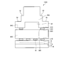
- FIG. 2A is a side view of the imaging module disposed at the distal end portion of the endoscope shown in FIG. 1 (before filling with an underfill agent).
- 2B is a diagram of a connection surface side (lower surface) of a circuit board used in the imaging module of FIG. 2A.
- FIG. 3A is a diagram illustrating filling of an underfill agent into a connection portion of a conventional imaging module.
- FIG. 3B is a side view of a conventional imaging module (after filling with an underfill agent).
- FIG. 1 is a diagram schematically illustrating the overall configuration of the endoscope system according to the first embodiment of the present invention.
- FIG. 2A is a side view of the imaging module disposed at the distal end portion of the endoscope shown in FIG. 1 (before filling with an underfill agent).
- 2B is a diagram of a connection surface
- FIG. 3C is a diagram illustrating filling of the underfill agent into the connection portion of the imaging module according to Embodiment 1 of the present invention.
- FIG. 3D is a side view of the imaging module according to Embodiment 1 of the present invention (after filling with an underfill agent).
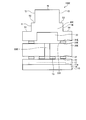
- FIG. 4 is a side view of the imaging module according to Modification 1 of Embodiment 1 of the present invention (before underfill agent filling).
- FIG. 5A is a side view of the imaging module according to Modification 2 of Embodiment 1 of the present invention (before underfill agent filling).
- FIG. 5B is a diagram of the connection surface side (lower surface) of the circuit board used in the imaging module of Modification 2 of Embodiment 1 of the present invention.
- FIG. 5C is a diagram illustrating filling of the underfill agent into the connection portion of the imaging module according to the second modification of the first embodiment of the present invention.
- FIG. 5D is a side view of the imaging module according to Modification 2 of Embodiment 1 of the present invention (after filling with an underfill agent).
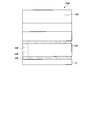
- FIG. 6A is a side view of the imaging module according to Embodiment 2 of the present invention (before underfill agent filling).
- FIG. 6B is a top view of the second circuit board used in the imaging module according to Embodiment 2 of the present invention.
- FIG. 6C is a side view of the imaging module according to Embodiment 2 of the present invention (after filling with an underfill agent).
- FIG. 7 is a side view of an imaging module according to Modification 1 of Embodiment 2 of the present invention.
- FIG. 8A is a side view of an imaging module according to Modification 2 of Embodiment 2 of the present invention (before underfill agent filling).
- FIG. 8B is a diagram illustrating filling of the underfill agent into the connection portion of the imaging module according to the second modification of the second embodiment of the present invention.
- FIG. 8C is a side view of the imaging module according to Modification 2 of Embodiment 2 of the present invention (after filling with an underfill agent).
- an endoscope system including an imaging module will be described as a mode for carrying out the present invention (hereinafter referred to as “embodiment”). Moreover, this invention is not limited by this embodiment. Furthermore, the same code
- FIG. 1 is a diagram schematically illustrating the overall configuration of the endoscope system according to the first embodiment of the present invention.
- an endoscope system 1 according to the first embodiment includes an endoscope 2 that is introduced into a subject, images the inside of the subject, and generates an image signal in the subject.
- An information processing device 3 that performs predetermined image processing on an image signal captured by the endoscope 2 and controls each part of the endoscope system 1, a light source device 4 that generates illumination light of the endoscope 2, and information And a display device 5 for displaying an image signal after image processing by the processing device 3.
- the endoscope 2 includes an insertion unit 6 to be inserted into a subject, an operation unit 7 on the proximal end side of the insertion unit 6 and held by an operator, and a flexible universal extending from the operation unit 7. Code 8 is provided.
- the insertion portion 6 is realized using an illumination fiber (light guide cable), an electric cable, an optical fiber, and the like.
- the insertion portion 6 has a distal end portion 6a in which an imaging unit to be described later is incorporated, a bendable bending portion 6b constituted by a plurality of bending pieces, and a flexibility provided on the proximal end side of the bending portion 6b.
- the distal end portion 6a includes an illumination unit that illuminates the inside of the subject via an illumination lens, an observation unit that images the inside of the subject, an opening that communicates with the treatment instrument channel, and an air / water supply nozzle (not shown). Is provided.
- the operation unit 7 includes a bending knob 7a that bends the bending portion 6b in the vertical direction and the left-right direction, a treatment instrument insertion portion 7b in which a treatment instrument such as a biological forceps and a laser knife is inserted into the body cavity of the subject, and an information processing device 3.
- a plurality of switch units 7c for operating peripheral devices such as the light source device 4, the air supply device, the water supply device, and the gas supply device.
- the treatment instrument inserted from the treatment instrument insertion portion 7b is exposed from the opening at the distal end of the insertion portion 6 through a treatment instrument channel provided therein.
- the universal cord 8 is configured using illumination fibers, cables, and the like.
- the universal cord 8 is branched at the base end, and one end of the branch is the connector 8a, and the other end is the connector 8b.
- the connector 8a is detachable from the information processing apparatus 3.
- the connector 8b is detachable from the light source device 4.
- the universal cord 8 propagates the illumination light emitted from the light source device 4 to the distal end portion 6a via the connector 8b and the illumination fiber.
- the universal code 8 transmits an image signal captured by an imaging module described later to the information processing apparatus 3 via the cable and the connector 8a.
- the information processing apparatus 3 performs predetermined image processing on the image signal output from the connector 8a and controls the entire endoscope system 1.
- the light source device 4 includes a light source that emits light, a condensing lens, and the like.
- the light source device 4 emits light from the light source under the control of the information processing device 3, and illuminates the inside of the subject, which is the subject, to the endoscope 2 connected via the connector 8b and the illumination fiber of the universal cord 8. Supply as light.
- the display device 5 is configured by using a display using liquid crystal or organic EL (Electro Luminescence).
- the display device 5 displays various types of information including images that have been subjected to predetermined image processing by the information processing device 3 via the video cable 5a. Thereby, the surgeon can observe and characterize a desired position in the subject by operating the endoscope 2 while viewing the image (in-vivo image) displayed on the display device 5.
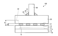
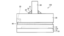
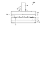
- FIG. 2A is a side view of the imaging module disposed at the distal end portion of the endoscope shown in FIG. 1 (before filling with an underfill agent).
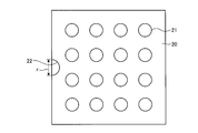
- 2B is a diagram of a connection surface side (lower surface) of a circuit board used in the imaging module of FIG. 2A.
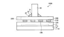
- the imaging module 100 includes an imaging element 11, a chip size package 10 in which a plurality of connection lands 12 are formed on the back side of the light receiving unit 11 a, and a plurality of connection electrodes 21, and the connection electrodes 21 are chip size packages.
- a first circuit board 20 electrically and mechanically connected to the ten connection lands 12 and the bumps 13; a second circuit board 30 disposed perpendicular to the first circuit board 20; And an underfill agent 40 filled in a connecting portion between the chip size package 10 and the first circuit board 20 (see FIG. 3D).
- the first circuit board 20 and the second circuit board 30 have a rectangular plate shape, and are connected in the projection plane in the optical axis direction of the image pickup device 11 of the chip size package 10 in a state where each part is connected as the image pickup module 100.
- a light receiving portion 11 a such as a CMOS element is formed on the surface of the image pickup device 11.
- the light receiving portion 11a is connected to the connection land 12 on the back surface side through a through wiring (not shown) formed by TSV (Through-Silicon Via) or the like.
- Bumps 13 made of solder are formed on the connection lands 12.
- a cover glass 14 that protects the light receiving portion 11 a is joined to the surface side of the image sensor 11.
- the first circuit board 20 has a plate shape in which a plurality of wirings are stacked via an insulating layer.
- a ceramic substrate, a glass epoxy substrate, a glass substrate, a silicon substrate, or the like is used as the first circuit board 20 .
- a connection electrode 21 is formed on the connection surface side of the first circuit board 20 with the chip size package 10 at a position corresponding to the connection land 12, and a connection electrode 23 is formed on the back surface side of the connection surface. Yes.
- the connection electrode 21 is electrically and mechanically connected to the connection land 12 and the bump 13. Further, a cutout portion 22 that opens to the connection surface side is formed on a side surface orthogonal to the connection surface of the first circuit board 20 with the chip size package 10.
- the second circuit board 30 has a plate shape in which a plurality of wirings are stacked via an insulating layer.
- a ceramic substrate, glass epoxy substrate, glass substrate, silicon substrate, or the like is used as the second circuit board 30 .
- a connection electrode 31 is formed at one end of the second circuit board 30 and is connected to the connection electrode 23 of the first circuit board 20 by solder 32.
- the connection between the first circuit board 20 and the second circuit board 30 is performed by applying an adhesive to a predetermined position of the first circuit board 20 and then placing the second circuit board 30 on the back surface of the first circuit board 20.
- the connection electrode 23 and the connection electrode 31 are connected to each other by the solder 32 after being temporarily fixed to the vertical (T-shaped).
- cables and electronic components are connected to the second circuit board 30.
- the electronic component may be mounted on the back surface side of the first circuit board 20 or may be incorporated in the first circuit board 20 and the second circuit board 30.
- the mounted cables and electronic components are preferably sized to fit within the projection plane in the optical axis direction of the image sensor 11 of the chip size package 10.
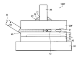
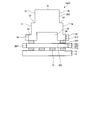
- FIG. 3A is a diagram illustrating filling of an underfill agent into a connection portion of a conventional imaging module.
- FIG. 3B is a side view of a conventional imaging module (after filling with an underfill agent).
- FIG. 3C is a diagram illustrating filling of the underfill agent into the connection portion of the imaging module according to Embodiment 1 of the present invention.
- FIG. 3D is a side view of the imaging module according to Embodiment 1 of the present invention (after filling with an underfill agent).
- the insertion portion 6 of the endoscope 2 has been reduced in diameter to reduce the burden on the specimen, and the chip size package 10 of the imaging module 100 has a side length of about 1 to 5 mm. Is used.
- the length g (see FIG. 2A) of the gap between the chip size package 10 and the first circuit board 20 is about 100 ⁇ m. Since the tip diameter of the nozzle 50 filling the underfill agent 40 is 100 to 150 ⁇ m, in the conventional imaging module 100F shown in FIG. 3A, the nozzle 50 is placed in the gap between the chip size package 10 and the first circuit board 20F. Cannot be inserted, and the underfill agent 40 is filled from the side surface direction of the gap. When the underfill agent 40 is filled from the side surface direction, the underfill agent 40 that cannot be filled in the gap remains on the side surface of the chip size package 10, and the diameter of the imaging module 100F is increased.
- a notch 22 is formed at the end of the side surface orthogonal to the connection surface of the first circuit board 20 so as to be cut out at least on the connection surface side.
- the tip of the nozzle 50 is inserted into the portion 22 to inject the underfill agent 40 into the gap (see FIG. 3C).
- the tip portion of the nozzle 50 is positioned in the projection plane in the optical axis direction of the image pickup device 11 of the chip size package 10 and is filled with the underfill agent 40, so that the underfill agent 40 extends in the side surface direction of the chip size package 10.
- the imaging module 100 can be reduced in diameter without leaking (see FIG. 3D).
- the underfill agent 40 is cured by heating at about 120 to 150 ° C. after filling the gap.
- the notch 22 may be of a size that allows the tip of the Nords 50 to be inserted.
- the diameter r of the notch 22 is not less than the nozzle tip diameter D + 10 ⁇ m, from the bottom of the notch 22 to the connection surface of the chip size package 10. It is preferable that the distance G is also the nozzle tip diameter D + 10 ⁇ m or more.
- the upper limit of the diameter r of the notch 22 is 20% or less, preferably 10% or less, of the length of one side of the first circuit board 20 from the viewpoint of strength and mounting density.
- the cutout portion 22 is preferably a semi-cylindrical shape from the viewpoint of ease of formation, but is not limited thereto, and may be a rectangular column or a triangular column (a taper is formed on the end surface of the first circuit board 20). Moreover, although the notch 22 is formed in the center part of one side of the 1st circuit board 20, you may form in a corner and may provide two or more notch parts 22. FIG.
- a notch 22 for inserting the tip of the nozzle 50 is provided on the side surface orthogonal to the connection surface of the first circuit board 20, and the gap between the chip size package 10 and the first circuit board 20 is provided. Since the underfill agent 40 can be filled through the notch 22, the underfill agent 40 does not leak out of the projection surface of the chip size package 10, that is, the optical axis direction of the image sensor 11 of the chip size package 10. Therefore, the imaging module 100 can be reduced in diameter. In addition, since the underfill agent 40 is filled in the gap between the chip size package 10 and the first circuit board 20, the reliability of the connection portion can be improved.
- FIG. 4 is a side view of the imaging module according to Modification 1 of Embodiment 1 of the present invention (before underfill agent filling).
- a solder resist layer 24 is formed on the connection surface side of the first circuit board 20A.
- the notch 22A is formed in the solder resist layer 24.
- the cutout portion 22A may be a semi-cylindrical shape as in the first embodiment, but without forming the solder resist layer 24 on one side of the first circuit board 20A, a portion where the solder resist layer 24 does not exist is formed. It may be used as a notch.
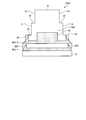
- FIG. 5A is a side view of the imaging module according to Modification 2 of Embodiment 1 of the present invention (before underfill agent filling).
- FIG. 5B is a diagram of the connection surface side (lower surface) of the circuit board used in the imaging module of Modification 2 of Embodiment 1 of the present invention.
- FIG. 5C is a diagram illustrating filling of the underfill agent into the connection portion of the imaging module according to the second modification of the first embodiment of the present invention.
- FIG. 5D is a side view of the imaging module according to Modification 2 of Embodiment 1 of the present invention (after filling with an underfill agent).
- the notch 22B is formed so as to penetrate from the connection surface with the chip size package 10 of the first circuit board 20B to the back surface side. .
- the notch 22B can be formed to penetrate the first circuit board 20B.
- the connection electrode 21B formed on the connection surface side of the first circuit board 20B with the chip size package 10 is disposed so as to avoid one side where the notch 22B is disposed.
- the connection land 12B connected to the connection electrode 21B via the bump 13B is also formed to correspond to the connection electrode 21B.
- the underfill agent 40 is filled by inserting the tip of the nozzle 50 into the notch 22B.
- the shape and size of the notch 22B are the same as in the first embodiment.
- the vicinity of the notch portion 22B to be injected and the side facing the notch portion 22B are preferably filled while observing in two fields of view.
- the underfill agent 40 forms a fillet shape in the notch 22B as the filling amount increases. Since the imaging element 11 of the package 10 does not protrude beyond the projection surface in the optical axis direction, the imaging module 100B can be reduced in diameter. Further, since the imaging module 100B has the notch 22B formed through the first circuit board 20B, the orientation of the imaging module 100B can be easily determined by the position of the notch 22B, and the assembling process It becomes easy to handle. Furthermore, in the imaging module 100B, since the connection electrode 21B is disposed so as to avoid the one side where the notch 22B is disposed, it is easy to form the notch 22B.
- FIG. 6A is a side view of the imaging module according to Embodiment 2 of the present invention (before underfill agent filling).
- FIG. 6B is a top view of the second circuit board used in the imaging module according to Embodiment 2 of the present invention.
- FIG. 6C is a side view of the imaging module according to Embodiment 2 of the present invention (after filling with an underfill agent).
- the first circuit board 20 ⁇ / b> C has a rectangular plate shape in which a plurality of wirings are stacked via an insulating layer, and each part is connected as the imaging module 100 ⁇ / b> C in the optical axis direction of the imaging element 11 of the chip size package 10.
- the size fits within the projection plane.
- a connection electrode 21C is formed at a position corresponding to the connection land 12 on the connection surface side of the first circuit board 20C with the chip size package 10, and a connection electrode 23C is formed on the back surface side of the connection surface.
- the connection electrode 21 ⁇ / b> C is electrically and mechanically connected via the connection land 12 and the bump 13. Further, notches 22C penetrating from the connection surface side to the back surface side of the first circuit board 20C are formed at the four corners of the first circuit board 20C.
- the second circuit board 30C has a left-right symmetrical variant in which a plurality of wirings are stacked via an insulating layer, and the optical axis of the image pickup device 11 of the chip size package 10 is connected to each part as the image pickup module 100C.
- the size is within the projection plane of the direction.
- an MID (Molded Interconnect Device) board in which a three-dimensional wiring is formed by injection molding can be used in addition to the board similar to the first embodiment.
- the second circuit board 30C has step portions 51, 52, 53 and 54 on the left and right.
- connection electrode 31C connected to the connection electrode 23C of the first circuit board 20C via the solder 32C is formed on the bottom surface side of the second circuit board 30C, and a recess 33 penetrating in the front-rear direction is formed. It is formed.
- An electronic component (not shown) is mounted in the space formed by the first circuit board 20 ⁇ / b> C and the recess 33.
- notches 34 are formed at the four corners of the second circuit board 30C so as to penetrate from the connection surface side of the second circuit board 30C to the first circuit board 20C to the step portion 51 or the step portion 54 side. ing.
- the second circuit board 30C includes a surface f1 between the step 51 and the step 52, a surface f2 between the step 52 and the upper surface f5, a surface f3 between the upper surface f5 and the step 53, and a step.
- a cable connection land (not shown) is formed on the surface f4 between the portion 53 and the step portion 54, and the cable is connected to the land.
- underfill agents 40C-1 and 40C- are applied to the connection portion between the chip size package 10 and the first circuit board 20C and the connection portion between the first circuit board 20C and the second circuit board 30C. 2 are filled respectively.
- Filling the connecting portion between the first circuit board 20C and the second circuit board 30C with the underfill agent 40C-2 inserts the tip of the nozzle into the recess 33 of the second circuit board 30C, and the tip of the nozzle 50
- the part is performed in a state where it is positioned within the projection plane in the optical axis direction of the first circuit board 20C.
- the filling of the underfill agent 40C-2 into the concave portion 33 is preferably performed while observing the two portions in the vicinity of the concave portion 33 on the injection side and the concave portion 33 on the side facing the concave portion 33 on the injection side.
- the nozzle 50 After filling the recess 33 with the underfill agent 40C-2, the nozzle 50 is moved to the notch 22C adjacent to the recess 33 to underfill the connection between the chip size package 10 and the first circuit board 20C. Agent 40C-1 is filled. The connecting portion between the chip size package 10 and the first circuit board 20C is filled with the underfill agent 40C-1, the tip of the nozzle 50 is inserted into the notch 22C, and the tip of the nozzle 50 is inserted into the chip size package. This is performed in a state where the ten image sensors 11 are positioned within the projection plane in the optical axis direction.
- the filling of the underfill agent 40C-1 is preferably performed while magnifying and observing the vicinity of the notch 22C to be injected and the side of the notch 22C facing the notch 22C to be injected in two fields of view.
- the underfill agent 40C-1 does not leak out in the side surface direction of the chip size package 10.
- the underfill agents 40C-1 and 40C-2 have a fillet shape in the notches 22C and 34 as shown in FIG. 6C. Since the ten imaging elements 11 do not protrude beyond the projection surface in the optical axis direction, the imaging module 100C can be reduced in diameter. Further, since the notches 22C and 34 are formed at the four corners of the first circuit board 20C and the second circuit board 30C, the connection between the first circuit board 20C and the second circuit board 30C, or the chip Even when a ⁇ shift occurs when the size package 10 and the first circuit board 20C are connected, the imaging module 100C can be prevented from increasing in diameter.
- the notch is formed so as to penetrate the first circuit board and the second circuit board, but may be a notch that does not penetrate.
- FIG. 7 is a side view of an imaging module according to Modification 1 of Embodiment 2 of the present invention.
- the first circuit board 20 ⁇ / b> D is formed with a notch 22 ⁇ / b> D that opens to the connection surface on the side surface orthogonal to the connection surface with the chip size package 10.
- One notch 22D is formed on one side of the first circuit board 20D, but may be formed on each side as long as the tip of the nozzle can be inserted, and at the four corners. Each may be formed.
- the second circuit board 30D is formed with a notch 34D that opens to the connection surface on a side surface orthogonal to the connection surface with the first circuit board 20D.
- One notch 34D is formed on one side of the second circuit board 30D, but may be formed on each side as long as the tip of the nozzle can be inserted, and at the four corners. Each may be formed.
- FIG. 8A is a side view of an imaging module according to Modification 2 of Embodiment 2 of the present invention (before underfill agent filling).
- FIG. 8B is a diagram illustrating filling of the underfill agent into the connection portion of the imaging module according to the second modification of the second embodiment of the present invention.
- FIG. 8C is a side view of the imaging module according to Modification 2 of Embodiment 2 of the present invention (after filling with an underfill agent).
- a cutout portion 22E penetrating from the connection surface side to the chip size package 10 to the connection surface side to the second circuit board 30E is formed on the side surface of the first circuit board 20E.
- the underfill agent 40E is filled in the connecting portion between the chip size package 10 and the first circuit board 20E and the connecting portion between the first circuit board 20E and the second circuit board 30E.
- the nozzle tip is inserted into the notch 22E formed in the first circuit board 20E, and the tip of the nozzle 50 is positioned in the projection plane of the chip size package 10 in the optical axis direction. .
- the tip of the nozzle 50 may be moved in the vertical direction within the notch 22E.
- the filling of the underfill agent 40E is preferably performed while magnifying and observing the vicinity of the notch 22E and the side facing the notch 22E in two fields of view. Thereby, the underfill agent 40E does not leak in the side surface direction of the chip size package 10.
- the underfill agent 40E protrudes outside the projection surface in the optical axis direction of the imaging element 11 of the chip size package 10, as shown in FIG. 8C. Therefore, the imaging module 100E can be reduced in diameter.
- the imaging module, endoscope system, and imaging module manufacturing method of the present invention are useful for an endoscope system that requires a high-quality image and a reduced diameter at the tip.
Abstract
Description
図1は、本発明の実施の形態1にかかる内視鏡システムの全体構成を模式的に示す図である。図1に示すように、本実施の形態1にかかる内視鏡システム1は、被検体内に導入され、被検体の体内を撮像して被検体内の画像信号を生成する内視鏡2と、内視鏡2が撮像した画像信号に所定の画像処理を施すとともに内視鏡システム1の各部を制御する情報処理装置3と、内視鏡2の照明光を生成する光源装置4と、情報処理装置3による画像処理後の画像信号を画像表示する表示装置5と、を備える。 (Embodiment 1)
FIG. 1 is a diagram schematically illustrating the overall configuration of the endoscope system according to the first embodiment of the present invention. As shown in FIG. 1, an
実施の形態2では、第2の回路基板として異形回路基板を使用する。図6Aは、本発明の実施の形態2にかかる撮像モジュールの側面図である(アンダーフィル剤充填前)。図6Bは、本発明の実施の形態2の撮像モジュールで使用する第2の回路基板の上面図である。図6Cは、本発明の実施の形態2にかかる撮像モジュールの側面図である(アンダーフィル剤充填後)。 (Embodiment 2)
In the second embodiment, a deformed circuit board is used as the second circuit board. FIG. 6A is a side view of the imaging module according to
2 内視鏡
3 情報処理装置
4 光源装置
5 表示装置
6 挿入部
6a 先端部
6b 湾曲部
6c 可撓管部
7 操作部
7a 湾曲ノブ
7b 処置具挿入部
7c スイッチ部
8 ユニバーサルコード
8a、8b コネクタ
10 チップサイズパッケージ
11 撮像素子
11a 受光部
12、12B 接続ランド
13、13B バンプ
14 カバーガラス
20、20A、20B、20C、20F 第1の回路基板
21、21B、21C、23、23C、31、31C 接続電極
22、22A、22B、22C、22D 切欠き部
24 ソルダーレジスト層
30、30C 第2の回路基板
32 はんだ
33 凹部
40、40C-1、40C-2、40E アンダーフィル剤
50 ノズル
51、52、53、54 段部
60 ホットプレート
100、100A、100B、100C、100D、100E、100F 撮像モジュール DESCRIPTION OF
Claims (7)
- 撮像素子を有し、前記撮像素子の受光部の裏面側に複数の接続ランドが配置されたチップサイズパッケージと、
複数の接続電極を有し、前記接続電極が前記チップサイズパッケージの前記接続ランドとバンプを介して電気的および機械的に接続される回路基板と、
前記チップサイズパッケージと前記回路基板との接続部に充填されたアンダーフィル剤と、を備え、
前記回路基板および前記アンダーフィル剤の前記チップサイズパッケージの前記撮像素子の光軸方向に投影した時の大きさは、前記チップサイズパッケージの光軸方向の投影面内に収まる形状をなし、
前記回路基板の前記チップサイズパッケージとの接続面と直交する側面に、少なくとも前記接続面に開口する切欠き部が形成されていることを特徴とする撮像モジュール。 A chip size package having an image sensor, and a plurality of connection lands arranged on the back side of the light receiving portion of the image sensor;
A circuit board having a plurality of connection electrodes, wherein the connection electrodes are electrically and mechanically connected to the connection lands of the chip size package via bumps;
An underfill agent filled in a connection portion between the chip size package and the circuit board;
The size of the circuit board and the underfill agent when projected in the optical axis direction of the imaging element of the chip size package is a shape that fits within the projection plane of the chip size package in the optical axis direction,
An imaging module, wherein at least a notch opening in the connection surface is formed on a side surface orthogonal to a connection surface with the chip size package of the circuit board. - 前記切欠き部は、前記回路基板の前記接続面側から前記接続面の裏面側まで貫通するよう形成されていることを特徴とする請求項1に記載の撮像モジュール。 The imaging module according to claim 1, wherein the notch is formed so as to penetrate from the connection surface side of the circuit board to the back surface side of the connection surface.
- 前記チップサイズパッケージは光軸方向の投影面が矩形をなし、
前記回路基板の前記複数の接続電極は、前記撮像素子の裏面側の前記切欠き部が配置される一辺側を避けるように配置されることを特徴とする請求項1または2に記載の撮像モジュール。 The chip size package has a rectangular projection surface in the optical axis direction,
3. The imaging module according to claim 1, wherein the plurality of connection electrodes of the circuit board are arranged so as to avoid one side where the notch portion on the back surface side of the imaging element is arranged. . - 前記回路基板は光軸方向の投影面が矩形をなし、
前記切欠き部は前記回路基板の矩形の四隅に形成されることを特徴とする請求項1または2に記載の撮像モジュール。 The circuit board has a rectangular projection surface in the optical axis direction,
The imaging module according to claim 1, wherein the notch is formed at a rectangular corner of the circuit board. - 前記回路基板は、前記チップサイズパッケージとの接続面側にソルダーレジスト層を有し、
前記切欠き部は、前記ソルダーレジスト層の側面に形成されることを特徴とする請求項1に記載の撮像モジュール。 The circuit board has a solder resist layer on the connection surface side with the chip size package,
The imaging module according to claim 1, wherein the notch is formed on a side surface of the solder resist layer. - 請求項1~5のいずれか一つに記載の撮像モジュールが先端に設けられた挿入部を備えたことを特徴とする内視鏡システム。 An endoscope system comprising an insertion portion provided at a tip of the imaging module according to any one of claims 1 to 5.
- 請求項1~5のいずれか一つに記載の撮像モジュールの製造方法であって、
チップサイズパッケージの裏面に形成された複数のバンプと、回路基板に形成された複数の接続電極とを、一括して接続する接続工程と、
前記回路基板の前記チップサイズパッケージとの接続面と直交する側面の一部に形成され、前記接続面側に開口する切欠き部にアンダーフィル剤を注入するノズル先端部を挿入することにより、前記チップサイズパッケージと前記回路基板との接続部の空隙にアンダーフィル剤を充填する封止工程と、
を含むことを特徴とする撮像モジュールの製造方法。 A method for manufacturing an imaging module according to any one of claims 1 to 5,
A connection step of connecting a plurality of bumps formed on the back surface of the chip size package and a plurality of connection electrodes formed on the circuit board in a lump;
By inserting a nozzle tip for injecting an underfill agent into a notch formed on a part of a side surface orthogonal to a connection surface with the chip size package of the circuit board, A sealing step of filling an underfill agent in a gap in a connection portion between the chip size package and the circuit board;
A method of manufacturing an imaging module, comprising:
Priority Applications (4)
| Application Number | Priority Date | Filing Date | Title |
|---|---|---|---|
| JP2016551343A JP6038424B1 (en) | 2015-06-16 | 2016-03-14 | Imaging module, endoscope system, and manufacturing method of imaging module |
| EP16811272.0A EP3170443B1 (en) | 2015-06-16 | 2016-03-14 | Imaging module, endoscope system, and method for manufacturing imaging module |
| CN201680002229.6A CN106793930B (en) | 2015-06-16 | 2016-03-14 | The manufacturing method of photographing module, endoscopic system and photographing module |
| US15/431,889 US20170150875A1 (en) | 2015-06-16 | 2017-02-14 | Imaging module, endoscope system, and method for manufacturing imaging module |
Applications Claiming Priority (2)
| Application Number | Priority Date | Filing Date | Title |
|---|---|---|---|
| JP2015121278 | 2015-06-16 | ||
| JP2015-121278 | 2015-06-16 |
Related Child Applications (1)
| Application Number | Title | Priority Date | Filing Date |
|---|---|---|---|
| US15/431,889 Continuation US20170150875A1 (en) | 2015-06-16 | 2017-02-14 | Imaging module, endoscope system, and method for manufacturing imaging module |
Publications (1)
| Publication Number | Publication Date |
|---|---|
| WO2016203797A1 true WO2016203797A1 (en) | 2016-12-22 |
Family
ID=57545538
Family Applications (1)
| Application Number | Title | Priority Date | Filing Date |
|---|---|---|---|
| PCT/JP2016/058006 WO2016203797A1 (en) | 2015-06-16 | 2016-03-14 | Imaging module, endoscope system, and method for manufacturing imaging module |
Country Status (4)
| Country | Link |
|---|---|
| US (1) | US20170150875A1 (en) |
| EP (1) | EP3170443B1 (en) |
| CN (1) | CN106793930B (en) |
| WO (1) | WO2016203797A1 (en) |
Cited By (4)
| Publication number | Priority date | Publication date | Assignee | Title |
|---|---|---|---|---|
| WO2021250727A1 (en) * | 2020-06-08 | 2021-12-16 | オリンパス株式会社 | Electronic module, method for manufacturing electronic module, and endoscope |
| US20230042245A1 (en) * | 2021-08-06 | 2023-02-09 | Altek Biotechnology Corporation | Image capturing assembly and related endoscope |
| WO2024013946A1 (en) * | 2022-07-14 | 2024-01-18 | オリンパスメディカルシステムズ株式会社 | Imaging unit and endoscope |
| WO2024028984A1 (en) * | 2022-08-02 | 2024-02-08 | オリンパスメディカルシステムズ株式会社 | Imaging unit and endoscope |
Families Citing this family (3)
| Publication number | Priority date | Publication date | Assignee | Title |
|---|---|---|---|---|
| WO2016111075A1 (en) * | 2015-01-05 | 2016-07-14 | オリンパス株式会社 | Imaging unit, imaging module and endoscopic system |
| US10665560B2 (en) * | 2017-10-27 | 2020-05-26 | Taiwan Semiconductor Manufacturing Company Ltd. | Optical semiconductor package and method for manufacturing the same |
| WO2020148820A1 (en) * | 2019-01-16 | 2020-07-23 | オリンパス株式会社 | Endoscope tip structure and endoscope |
Citations (3)
| Publication number | Priority date | Publication date | Assignee | Title |
|---|---|---|---|---|
| JP2010050260A (en) * | 2008-08-21 | 2010-03-04 | Zycube:Kk | Semiconductor image sensor |
| JP2014108282A (en) * | 2012-12-03 | 2014-06-12 | Olympus Corp | Imaging device, endoscope, and method for manufacturing imaging device |
| JP2014204275A (en) * | 2013-04-04 | 2014-10-27 | オリンパス株式会社 | Imaging apparatus, manufacturing method of imaging apparatus, and imaging module |
Family Cites Families (20)
| Publication number | Priority date | Publication date | Assignee | Title |
|---|---|---|---|---|
| JPH10270477A (en) * | 1997-03-27 | 1998-10-09 | Hitachi Ltd | Manufacture of semiconductor package |
| JP4004705B2 (en) * | 2000-02-29 | 2007-11-07 | 松下電器産業株式会社 | Imaging device and imaging device assembling method |
| US6825540B2 (en) * | 2001-12-05 | 2004-11-30 | Matsushita Electric Industrial Co., Ltd. | Miniaturized, resin-sealed solid state imaging apparatus |
| JP2004214344A (en) * | 2002-12-27 | 2004-07-29 | Nec Kansai Ltd | Solid-state imaging device |
| US6953891B2 (en) * | 2003-09-16 | 2005-10-11 | Micron Technology, Inc. | Moisture-resistant electronic device package and methods of assembly |
| JP2005183545A (en) * | 2003-12-17 | 2005-07-07 | Kuroda Techno Co Ltd | Light receiving module |
| US7170183B1 (en) * | 2005-05-13 | 2007-01-30 | Amkor Technology, Inc. | Wafer level stacked package |
| KR101409839B1 (en) * | 2007-05-23 | 2014-06-26 | 삼성전자주식회사 | Semiconductor package |
| US20090079863A1 (en) * | 2007-09-20 | 2009-03-26 | Susumu Aoki | Camera module, manufacturing method of imaging apparatus and hot melt molding method |
| US8188142B2 (en) * | 2008-01-16 | 2012-05-29 | The United States Of America, As Represented By The Secretary Of The Navy | Polymers from propenyl ether monomers |
| JP2009182155A (en) * | 2008-01-30 | 2009-08-13 | Nec Corp | Lsi package and lsi package loading type electronic component |
| JP2010057960A (en) * | 2009-12-14 | 2010-03-18 | Olympus Corp | Endoscope |
| US8698887B2 (en) * | 2010-04-07 | 2014-04-15 | Olympus Corporation | Image pickup apparatus, endoscope and manufacturing method for image pickup apparatus |
| US8574513B2 (en) * | 2011-04-20 | 2013-11-05 | California Institute Of Technology | Single-layer PCB microfluidics |
| JP6003194B2 (en) * | 2012-04-27 | 2016-10-05 | セイコーエプソン株式会社 | Base substrate, electronic device, and method of manufacturing base substrate |
| CN104380465B (en) * | 2012-05-30 | 2018-02-09 | 奥林巴斯株式会社 | The manufacture method of camera device and the manufacture method of semiconductor device |
| WO2013179766A1 (en) * | 2012-05-30 | 2013-12-05 | オリンパス株式会社 | Imaging device, semiconductor device, and imaging unit |
| JPWO2014155405A1 (en) * | 2013-03-25 | 2017-02-16 | 株式会社東芝 | Wiring cable connection structure and wiring cable connection method |
| JP6396650B2 (en) * | 2013-09-30 | 2018-09-26 | オリンパス株式会社 | Imaging unit and endoscope apparatus |
| JP6316979B2 (en) * | 2014-10-16 | 2018-04-25 | シャープ株式会社 | Camera module manufacturing method and manufacturing apparatus |
-
2016
- 2016-03-14 EP EP16811272.0A patent/EP3170443B1/en not_active Not-in-force
- 2016-03-14 CN CN201680002229.6A patent/CN106793930B/en active Active
- 2016-03-14 WO PCT/JP2016/058006 patent/WO2016203797A1/en active Application Filing
-
2017
- 2017-02-14 US US15/431,889 patent/US20170150875A1/en not_active Abandoned
Patent Citations (3)
| Publication number | Priority date | Publication date | Assignee | Title |
|---|---|---|---|---|
| JP2010050260A (en) * | 2008-08-21 | 2010-03-04 | Zycube:Kk | Semiconductor image sensor |
| JP2014108282A (en) * | 2012-12-03 | 2014-06-12 | Olympus Corp | Imaging device, endoscope, and method for manufacturing imaging device |
| JP2014204275A (en) * | 2013-04-04 | 2014-10-27 | オリンパス株式会社 | Imaging apparatus, manufacturing method of imaging apparatus, and imaging module |
Non-Patent Citations (1)
| Title |
|---|
| See also references of EP3170443A4 * |
Cited By (5)
| Publication number | Priority date | Publication date | Assignee | Title |
|---|---|---|---|---|
| WO2021250727A1 (en) * | 2020-06-08 | 2021-12-16 | オリンパス株式会社 | Electronic module, method for manufacturing electronic module, and endoscope |
| US20230042245A1 (en) * | 2021-08-06 | 2023-02-09 | Altek Biotechnology Corporation | Image capturing assembly and related endoscope |
| US11662567B2 (en) * | 2021-08-06 | 2023-05-30 | Altek Biotechnology Corporation | Image capturing assembly and related endoscope |
| WO2024013946A1 (en) * | 2022-07-14 | 2024-01-18 | オリンパスメディカルシステムズ株式会社 | Imaging unit and endoscope |
| WO2024028984A1 (en) * | 2022-08-02 | 2024-02-08 | オリンパスメディカルシステムズ株式会社 | Imaging unit and endoscope |
Also Published As
| Publication number | Publication date |
|---|---|
| US20170150875A1 (en) | 2017-06-01 |
| EP3170443A1 (en) | 2017-05-24 |
| CN106793930A (en) | 2017-05-31 |
| EP3170443B1 (en) | 2019-01-02 |
| EP3170443A4 (en) | 2018-05-30 |
| CN106793930B (en) | 2018-08-07 |
Similar Documents
| Publication | Publication Date | Title |
|---|---|---|
| WO2016203797A1 (en) | Imaging module, endoscope system, and method for manufacturing imaging module | |
| JP5964003B1 (en) | Imaging unit, imaging module, and endoscope system | |
| CN108778094B (en) | Imaging unit and endoscope | |
| JP6307697B1 (en) | Electronic circuit unit, imaging unit, imaging module, and endoscope | |
| US20160037029A1 (en) | Image pickup apparatus and electronic endoscope | |
| US10362929B2 (en) | Imaging unit, imaging module, and endoscope | |
| JP2017023234A (en) | Imaging unit and endoscope | |
| JP6038424B1 (en) | Imaging module, endoscope system, and manufacturing method of imaging module | |
| JP6324644B1 (en) | Imaging unit and endoscope | |
| WO2017130887A1 (en) | Imaging unit, imaging module, and endoscope | |
| JPWO2018230368A1 (en) | Imaging unit and endoscope | |
| WO2018079328A1 (en) | Image capture unit and endoscope system | |
| JP6165402B1 (en) | Imaging unit, imaging module, and endoscope | |
| JP6486584B2 (en) | Imaging unit and endoscope | |
| JP2017217080A (en) | Endoscope | |
| JP6324639B1 (en) | Imaging unit and endoscope | |
| JP6297240B1 (en) | Electronic circuit unit, imaging unit and endoscope | |
| WO2024028984A1 (en) | Imaging unit and endoscope | |
| JP6165395B1 (en) | Imaging unit, imaging module, and endoscope |
Legal Events
| Date | Code | Title | Description |
|---|---|---|---|
| ENP | Entry into the national phase |
Ref document number: 2016551343 Country of ref document: JP Kind code of ref document: A |
|
| 121 | Ep: the epo has been informed by wipo that ep was designated in this application |
Ref document number: 16811272 Country of ref document: EP Kind code of ref document: A1 |
|
| REEP | Request for entry into the european phase |
Ref document number: 2016811272 Country of ref document: EP |
|
| WWE | Wipo information: entry into national phase |
Ref document number: 2016811272 Country of ref document: EP |
|
| NENP | Non-entry into the national phase |
Ref country code: DE |